EP3657654A1 - Direct current voltage conversion circuit, direct current voltage conversion method, and liquid crystal display device - Google Patents
Direct current voltage conversion circuit, direct current voltage conversion method, and liquid crystal display device Download PDFInfo
- Publication number
- EP3657654A1 EP3657654A1 EP17918340.5A EP17918340A EP3657654A1 EP 3657654 A1 EP3657654 A1 EP 3657654A1 EP 17918340 A EP17918340 A EP 17918340A EP 3657654 A1 EP3657654 A1 EP 3657654A1
- Authority
- EP
- European Patent Office
- Prior art keywords
- voltage
- diode
- capacitor
- cathode
- terminal
- Prior art date
- Legal status (The legal status is an assumption and is not a legal conclusion. Google has not performed a legal analysis and makes no representation as to the accuracy of the status listed.)
- Withdrawn
Links
- 238000006243 chemical reaction Methods 0.000 title claims abstract description 57
- 239000004973 liquid crystal related substance Substances 0.000 title claims abstract description 21
- 238000000034 method Methods 0.000 title claims abstract description 17
- 239000003990 capacitor Substances 0.000 claims abstract description 161
- 230000005669 field effect Effects 0.000 claims description 9
- 102100029092 Utrophin Human genes 0.000 abstract description 42
- 101001044612 Homo sapiens Density-regulated protein Proteins 0.000 abstract description 34
- 101000909218 Homo sapiens Dynamin-1-like protein Proteins 0.000 abstract description 34
- 101000841301 Homo sapiens Utrophin Proteins 0.000 abstract description 34
- 102100020767 Dystrophin-related protein 2 Human genes 0.000 abstract description 19
- 101001053503 Homo sapiens Dihydropyrimidinase-related protein 2 Proteins 0.000 abstract description 19
- 101000931797 Homo sapiens Dystrophin-related protein 2 Proteins 0.000 abstract description 19
- 230000009466 transformation Effects 0.000 abstract description 11
- 230000001747 exhibiting effect Effects 0.000 abstract 1
- 101710092028 Density-regulated protein Proteins 0.000 description 8
- 239000000758 substrate Substances 0.000 description 7
- 238000010586 diagram Methods 0.000 description 5
- 101150056585 DACT2 gene Proteins 0.000 description 4
- 238000012986 modification Methods 0.000 description 2
- 230000004048 modification Effects 0.000 description 2
- 230000009286 beneficial effect Effects 0.000 description 1
- 239000008358 core component Substances 0.000 description 1
- 230000000694 effects Effects 0.000 description 1
- 230000005684 electric field Effects 0.000 description 1
- 230000010287 polarization Effects 0.000 description 1
- 239000010409 thin film Substances 0.000 description 1
Images



Classifications
-
- G—PHYSICS
- G09—EDUCATION; CRYPTOGRAPHY; DISPLAY; ADVERTISING; SEALS
- G09G—ARRANGEMENTS OR CIRCUITS FOR CONTROL OF INDICATING DEVICES USING STATIC MEANS TO PRESENT VARIABLE INFORMATION
- G09G3/00—Control arrangements or circuits, of interest only in connection with visual indicators other than cathode-ray tubes
- G09G3/20—Control arrangements or circuits, of interest only in connection with visual indicators other than cathode-ray tubes for presentation of an assembly of a number of characters, e.g. a page, by composing the assembly by combination of individual elements arranged in a matrix no fixed position being assigned to or needed to be assigned to the individual characters or partial characters
- G09G3/34—Control arrangements or circuits, of interest only in connection with visual indicators other than cathode-ray tubes for presentation of an assembly of a number of characters, e.g. a page, by composing the assembly by combination of individual elements arranged in a matrix no fixed position being assigned to or needed to be assigned to the individual characters or partial characters by control of light from an independent source
- G09G3/36—Control arrangements or circuits, of interest only in connection with visual indicators other than cathode-ray tubes for presentation of an assembly of a number of characters, e.g. a page, by composing the assembly by combination of individual elements arranged in a matrix no fixed position being assigned to or needed to be assigned to the individual characters or partial characters by control of light from an independent source using liquid crystals
-
- G—PHYSICS
- G09—EDUCATION; CRYPTOGRAPHY; DISPLAY; ADVERTISING; SEALS
- G09G—ARRANGEMENTS OR CIRCUITS FOR CONTROL OF INDICATING DEVICES USING STATIC MEANS TO PRESENT VARIABLE INFORMATION
- G09G3/00—Control arrangements or circuits, of interest only in connection with visual indicators other than cathode-ray tubes
- G09G3/20—Control arrangements or circuits, of interest only in connection with visual indicators other than cathode-ray tubes for presentation of an assembly of a number of characters, e.g. a page, by composing the assembly by combination of individual elements arranged in a matrix no fixed position being assigned to or needed to be assigned to the individual characters or partial characters
-
- G—PHYSICS
- G09—EDUCATION; CRYPTOGRAPHY; DISPLAY; ADVERTISING; SEALS
- G09G—ARRANGEMENTS OR CIRCUITS FOR CONTROL OF INDICATING DEVICES USING STATIC MEANS TO PRESENT VARIABLE INFORMATION
- G09G3/00—Control arrangements or circuits, of interest only in connection with visual indicators other than cathode-ray tubes
- G09G3/20—Control arrangements or circuits, of interest only in connection with visual indicators other than cathode-ray tubes for presentation of an assembly of a number of characters, e.g. a page, by composing the assembly by combination of individual elements arranged in a matrix no fixed position being assigned to or needed to be assigned to the individual characters or partial characters
- G09G3/34—Control arrangements or circuits, of interest only in connection with visual indicators other than cathode-ray tubes for presentation of an assembly of a number of characters, e.g. a page, by composing the assembly by combination of individual elements arranged in a matrix no fixed position being assigned to or needed to be assigned to the individual characters or partial characters by control of light from an independent source
- G09G3/36—Control arrangements or circuits, of interest only in connection with visual indicators other than cathode-ray tubes for presentation of an assembly of a number of characters, e.g. a page, by composing the assembly by combination of individual elements arranged in a matrix no fixed position being assigned to or needed to be assigned to the individual characters or partial characters by control of light from an independent source using liquid crystals
- G09G3/3611—Control of matrices with row and column drivers
- G09G3/3696—Generation of voltages supplied to electrode drivers
-
- H—ELECTRICITY
- H02—GENERATION; CONVERSION OR DISTRIBUTION OF ELECTRIC POWER
- H02M—APPARATUS FOR CONVERSION BETWEEN AC AND AC, BETWEEN AC AND DC, OR BETWEEN DC AND DC, AND FOR USE WITH MAINS OR SIMILAR POWER SUPPLY SYSTEMS; CONVERSION OF DC OR AC INPUT POWER INTO SURGE OUTPUT POWER; CONTROL OR REGULATION THEREOF
- H02M3/00—Conversion of DC power input into DC power output
- H02M3/02—Conversion of DC power input into DC power output without intermediate conversion into AC
- H02M3/04—Conversion of DC power input into DC power output without intermediate conversion into AC by static converters
- H02M3/06—Conversion of DC power input into DC power output without intermediate conversion into AC by static converters using resistors or capacitors, e.g. potential divider
- H02M3/07—Conversion of DC power input into DC power output without intermediate conversion into AC by static converters using resistors or capacitors, e.g. potential divider using capacitors charged and discharged alternately by semiconductor devices with control electrode, e.g. charge pumps
-
- H—ELECTRICITY
- H02—GENERATION; CONVERSION OR DISTRIBUTION OF ELECTRIC POWER
- H02M—APPARATUS FOR CONVERSION BETWEEN AC AND AC, BETWEEN AC AND DC, OR BETWEEN DC AND DC, AND FOR USE WITH MAINS OR SIMILAR POWER SUPPLY SYSTEMS; CONVERSION OF DC OR AC INPUT POWER INTO SURGE OUTPUT POWER; CONTROL OR REGULATION THEREOF
- H02M3/00—Conversion of DC power input into DC power output
- H02M3/02—Conversion of DC power input into DC power output without intermediate conversion into AC
- H02M3/04—Conversion of DC power input into DC power output without intermediate conversion into AC by static converters
- H02M3/06—Conversion of DC power input into DC power output without intermediate conversion into AC by static converters using resistors or capacitors, e.g. potential divider
- H02M3/07—Conversion of DC power input into DC power output without intermediate conversion into AC by static converters using resistors or capacitors, e.g. potential divider using capacitors charged and discharged alternately by semiconductor devices with control electrode, e.g. charge pumps
- H02M3/073—Charge pumps of the Schenkel-type
- H02M3/077—Charge pumps of the Schenkel-type with parallel connected charge pump stages
-
- H—ELECTRICITY
- H02—GENERATION; CONVERSION OR DISTRIBUTION OF ELECTRIC POWER
- H02M—APPARATUS FOR CONVERSION BETWEEN AC AND AC, BETWEEN AC AND DC, OR BETWEEN DC AND DC, AND FOR USE WITH MAINS OR SIMILAR POWER SUPPLY SYSTEMS; CONVERSION OF DC OR AC INPUT POWER INTO SURGE OUTPUT POWER; CONTROL OR REGULATION THEREOF
- H02M3/00—Conversion of DC power input into DC power output
- H02M3/02—Conversion of DC power input into DC power output without intermediate conversion into AC
- H02M3/04—Conversion of DC power input into DC power output without intermediate conversion into AC by static converters
- H02M3/08—Conversion of DC power input into DC power output without intermediate conversion into AC by static converters using discharge tubes without control electrode or semiconductor devices without control electrode
-
- G—PHYSICS
- G09—EDUCATION; CRYPTOGRAPHY; DISPLAY; ADVERTISING; SEALS
- G09G—ARRANGEMENTS OR CIRCUITS FOR CONTROL OF INDICATING DEVICES USING STATIC MEANS TO PRESENT VARIABLE INFORMATION
- G09G2320/00—Control of display operating conditions
- G09G2320/02—Improving the quality of display appearance
- G09G2320/0204—Compensation of DC component across the pixels in flat panels
-
- G—PHYSICS
- G09—EDUCATION; CRYPTOGRAPHY; DISPLAY; ADVERTISING; SEALS
- G09G—ARRANGEMENTS OR CIRCUITS FOR CONTROL OF INDICATING DEVICES USING STATIC MEANS TO PRESENT VARIABLE INFORMATION
- G09G2320/00—Control of display operating conditions
- G09G2320/02—Improving the quality of display appearance
- G09G2320/0252—Improving the response speed
-
- G—PHYSICS
- G09—EDUCATION; CRYPTOGRAPHY; DISPLAY; ADVERTISING; SEALS
- G09G—ARRANGEMENTS OR CIRCUITS FOR CONTROL OF INDICATING DEVICES USING STATIC MEANS TO PRESENT VARIABLE INFORMATION
- G09G2330/00—Aspects of power supply; Aspects of display protection and defect management
- G09G2330/02—Details of power systems and of start or stop of display operation
-
- G—PHYSICS
- G09—EDUCATION; CRYPTOGRAPHY; DISPLAY; ADVERTISING; SEALS
- G09G—ARRANGEMENTS OR CIRCUITS FOR CONTROL OF INDICATING DEVICES USING STATIC MEANS TO PRESENT VARIABLE INFORMATION
- G09G2330/00—Aspects of power supply; Aspects of display protection and defect management
- G09G2330/02—Details of power systems and of start or stop of display operation
- G09G2330/028—Generation of voltages supplied to electrode drivers in a matrix display other than LCD
Definitions
- the present invention relates to the field of liquid crystal display, and more particularly to a DC voltage conversion circuit, a DC voltage conversion method and a liquid crystal display device.
- the Liquid crystal display (Liquid Crystal Display, LCD) is one of the most widely used flat panel display device, the liquid crystal panel is a core component of liquid crystal display device.
- the liquid crystal panel is constituted of a color filter substrate (CF Substrate), a thin film transistor array substrate (TFT Array Substrate), and a liquid crystal layer (Liquid Crystal Layer) disposed between the two substrates.
- CF Substrate color filter substrate
- TFT Array Substrate thin film transistor array substrate
- Liquid Crystal Layer liquid crystal layer
- an array substrate and a CF substrate are provided with pixel electrodes and common electrodes.
- the voltages include a power supply voltage (VDD), a constant high voltage (VGH), and a constant low voltage (VGL).
- VDD power supply voltage
- VGH constant high voltage
- VGL constant low voltage
- VGH and VGL correspond with smaller currents, which are generally generated by charge pumps which are low-cost.
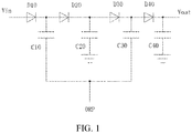
- Fig. 1 is charge pump circuit for generating a constant high-level voltage, which comprises a first diode D10, a second diode D20, a third diode D30, a fourth diode D40, a first capacitor C10, a second capacitor C20, a third capacitor C30, and a fourth capacitor C40.
- an anode of the first diode D10 is connected with an input voltage Vin and a cathode of the first diode D10 is electrically connected with an anode of the second diode D20, a cathode of the second diode D20 is electrically connected with an anode of the third diode D30 and a cathode of the third diode D30 is electrically connected with an anode of the fourth diode D40, a cathode of the fourth diode D40 outputs an output voltage Vout.
- a first terminal of the first capacitor C10 is electrically connected with the cathode of the first diode D10, a second terminal of the first capacitor C10 is connected with a voltage-transforming signal DRP.
- a first terminal of the second capacitor C20 is electrically connected with the cathode of the second diode D20 and a second terminal of the second capacitor C20 is grounded.
- a first terminal of the third capacitor C30 is electrically connected with the cathode of the third diode D30 and a second terminal of the third capacitor C30 is connected with the voltage-transforming signal DRP.
- a first terminal of the fourth capacitor C40 is electrically connected with the cathode of the fourth diode D40 and the second terminal of the fourth capacitor C40 is grounded.
- the voltage-transforming signal DRP is a pulse signal with alternative low-level and high-level, the voltage of the low-level is 0 volt, the high voltage is equal to the input voltage Vin.
- the voltage-transforming DRP when the charge pump circuit boosts the input voltage Vin, the voltage-transforming DRP is 0 volt, cathode voltages V10, V20, V30 of the first, second, and third diodes D10, D20, D30 and the cathode voltage of the fourth diode D40 (the output voltage Vout) all are the input voltages Vin. Then, the voltage-transforming signal DRP becomes the input voltage Vin, the cathode voltages V10, V20, V30 of the first, second, and third diodes D10, D20, D30 and the cathode voltage of the fourth diode D40 (the output voltage Vout) all become to twice of the input voltages Vin.
- the voltage-transforming signal DRP becomes 0 volt
- the cathode voltages V10, V20, V30 of the first, second, and third diodes D10, D20, D30 and the cathode voltage of the fourth diode D40 (the output voltage Vout) all keep as twice the input voltages Vin.
- the voltage-transforming signal DRP becomes the input voltage Vin again
- the cathode voltage V30 of the third diodes D30 and the cathode voltage of the fourth diode D40 (the output voltage Vout) both become as three times of the input voltages Vin. In other words, it takes two cycles of the voltage-transforming signal DRP to complete the boost of the input voltage Vin, the driving capability is insufficient and the response speed is slow.
- An object of the present invention is to provide a DC voltage conversion circuit, which can quickly complete the conversion of the input voltage with strong driving ability and fast response speed.
- Another object of the present invention is to provide a DC voltage conversion method, which can quickly complete the conversion of the input voltage with strong driving ability and fast response speed.
- Another object of the present invention is to provide a liquid crystal display device, which has strong driving ability and fast response speed.
- the present invention provides a DC voltage conversion circuit, which comprises a first diode, a second diode, a third diode, a fourth diode, a first capacitor, a second capacitor, a third capacitor, a fourth capacitor, a voltage dividing unit, and a switching unit.
- An anode of the first diode is connected with an input voltage and a cathode of the first diode is electrically connected with an anode of the second diode.
- a cathode of the second diode is electrically connected with an anode of the third diode.
- a cathode of the third diode is electrically connected with an anode of the fourth diode.
- a cathode of the fourth diode outputs an output voltage.
- a first terminal of the voltage dividing unit electrically connected with the anode of the first diode, a second terminal of the voltage dividing unit is connected with a drain electrode of the switching unit.
- a gate electrode of the switching unit is connected with a first voltage-transforming signal, a source electrode of the switching unit is grounded, and the drain electrode of the switching unit is also connected with a second voltage-transforming signal.
- a first terminal of the first capacitor is electrically connected with the cathode of the first diode and a second terminal of the first capacitor is connected with the first voltage-transforming signal.
- a first terminal of the second capacitor is electrically connected with the cathode of the second diode and a second terminal of the second capacitor is grounded.
- a first terminal of the third capacitor is electrically connected with the cathode of the third diode and a second terminal of the third capacitor is electrically connects the drain electrode of the switching unit.
- a first terminal of the fourth capacitor is electrically connected with the cathode of the fourth diode, a second terminal of the fourth capacitor is grounded.
- the first voltage-transforming signal is a pulse signal with alternative low-level and high-level, or the first voltage-transforming signal is a pulse signal with alternative high-level and low-level.
- the first voltage-transforming signal and the second voltage-transforming signal have opposite phases.
- a high level voltage of the first voltage-transforming signal is equal to the input voltage and a low level voltage of the first voltage-transforming signal is 0 volt.
- the voltage dividing unit is a resistor.
- the switching unit is a N-type field effect transistor.
- the present invention further provides a DC voltage conversion method, which comprises: Step S1, providing a DC voltage conversion circuit, which comprises a first diode, a second diode, a third diode, a fourth diode, a first capacitor, a second capacitor, a third capacitor, a fourth capacitor, a voltage dividing unit, and a switching unit.
- Step S1 providing a DC voltage conversion circuit, which comprises a first diode, a second diode, a third diode, a fourth diode, a first capacitor, a second capacitor, a third capacitor, a fourth capacitor, a voltage dividing unit, and a switching unit.
- An anode of the first diode is connected with an input voltage and a cathode of the first diode is electrically connected with an anode of the second diode.
- a cathode of the second diode is electrically connected with an anode of the third diode.
- a cathode of the third diode is electrically connected with an anode of the fourth diode.
- a cathode of the fourth diode outputs an output voltage.
- a first terminal of the voltage dividing unit electrically connected with the anode of the first diode, a second terminal of the voltage dividing unit is connected with a drain electrode of the switching unit.
- a gate electrode of the switching unit is connected with a first voltage-transforming signal, a source electrode of the switching unit is grounded, and the drain electrode of the switching unit is also connected with a second voltage-transforming signal.
- a first terminal of the first capacitor is electrically connected with the cathode of the first diode and a second terminal of the first capacitor is connected with the first voltage-transforming signal.
- a first terminal of the second capacitor is electrically connected with the cathode of the second diode and a second terminal of the second capacitor is grounded.
- a first terminal of the third capacitor is electrically connected with the cathode of the third diode and a second terminal of the third capacitor is electrically connects the drain electrode of the switching unit.
- a first terminal of the fourth capacitor is electrically connected with the cathode of the fourth diode, a second terminal of the fourth capacitor is grounded.
- Step S2 the first voltage-transforming signal is 0 volt, the second voltage-transforming signal is the input voltage, an cathode voltage of the fourth diode is twice the input voltage.
- Step S3 the first voltage-transforming signal is changed into the input voltage, the second voltage-transforming signal is changed into 0 volt, and the cathode voltage of the fourth diode is kept as twice the input voltage.
- Step S4 the first voltage-transforming signal is changed into 0 volt, the second voltage-transforming signal is changed into the input voltage, and the cathode voltage of the fourth diode is changed into three times the input voltage.
- the voltage dividing unit is a resistor.
- the switching unit is a N-type field effect transistor.
- the present invention further provides a DC voltage conversion method, which comprises: Step S1', providing a DC voltage conversion circuit, which comprises a first diode, a second diode, a third diode, a fourth diode, a first capacitor, a second capacitor, a third capacitor, a fourth capacitor, a voltage dividing unit, and a switching unit.
- Step S1' providing a DC voltage conversion circuit, which comprises a first diode, a second diode, a third diode, a fourth diode, a first capacitor, a second capacitor, a third capacitor, a fourth capacitor, a voltage dividing unit, and a switching unit.
- An anode of the first diode is connected with an input voltage and a cathode of the first diode is electrically connected with an anode of the second diode.
- a cathode of the second diode is electrically connected with an anode of the third diode.
- a cathode of the third diode is electrically connected with an anode of the fourth diode.
- a cathode of the fourth diode outputs an output voltage.
- a first terminal of the voltage dividing unit electrically connected with the anode of the first diode, a second terminal of the voltage dividing unit is connected with a drain electrode of the switching unit.
- a gate electrode of the switching unit is connected with a first voltage-transforming signal, a source electrode of the switching unit is grounded, and the drain electrode of the switching unit is also connected with a second voltage-transforming signal.
- a first terminal of the first capacitor is electrically connected with the cathode of the first diode and a second terminal of the first capacitor is connected with the first voltage-transforming signal.
- a first terminal of the second capacitor is electrically connected with the cathode of the second diode and a second terminal of the second capacitor is grounded.
- a first terminal of the third capacitor is electrically connected with the cathode of the third diode and a second terminal of the third capacitor is electrically connects the drain electrode of the switching unit.
- a first terminal of the fourth capacitor is electrically connected with the cathode of the fourth diode, a second terminal of the fourth capacitor is grounded.
- Step S2' the first voltage-transforming signal is the input voltage
- the second voltage-transforming signal is 0 volt
- an cathode voltage of the fourth diode is twice the input voltage.
- Step S3' the first voltage-transforming signal is changed into 0 volt, the second voltage-transforming signal is changed into twice the input voltage, and the cathode voltage of the fourth diode is changed into three times the input voltage.
- the voltage dividing unit is a resistor.
- the switching unit is a N-type field effect transistor.
- the present invention further provides a liquid crystal display device, which comprises the above DC voltage conversion circuit.
- the present invention provides a DC voltage conversion circuit, which comprises a first diode, a second diode, a third diode, a fourth diode, a first capacitor, a second capacitor, a third capacitor, a fourth capacitor, a voltage dividing unit, and a switching unit.
- the second terminal of the first capacitor is connected with the first voltage-transforming signal and the second terminal of the third capacitor is connected with the second voltage-transforming signal.
- the first and second voltage-transforming signals are both pulse signals, and the first and second voltage-transforming signals have opposite phases.
- the present invention can quickly complete the transformation of the input voltage, to reduce the require time for completing the voltage transformation, which has strong driving capability and fast response speed.
- the present invention provides a DC voltage conversion method, which can quickly complete the conversion of the input voltage with strong driving ability and fast response speed.
- the present invention provides a liquid crystal display device, which has strong driving ability and fast response speed.
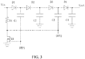
- the present invention provides a DC voltage conversion circuit, which comprises a first diode D1, a second diode D2, a third diode D3, a fourth diode D4, a first capacitor C1, a second capacitor C2, a third capacitor C3, a fourth capacitor C4, a voltage dividing unit R1, and a switching unit Q1.
- An anode of the first diode D1 is connected with an input voltage Vin and a cathode of the first diode D1 is electrically connected with an anode of the second diode D2.
- a cathode of the second diode D2 is electrically connected with an anode of the third diode D3.
- a cathode of the third diode D3 is electrically connected with an anode of the fourth diode D4.
- a cathode of the fourth diode D4 outputs an output voltage Vout.
- a first terminal of the voltage dividing unit R1 electrically connected with the anode of the first diode D1, a second terminal of the voltage dividing unit R1 is connected with a drain electrode of the switching unit Q1.
- a gate electrode of the switching unit Q1 is connected with a first voltage-transforming signal DRP1, a source electrode of the switching unit Q1 is grounded, and the drain electrode of the switching unit Q1 is also connected with a second voltage-transforming signal DRP2.
- a first terminal of the first capacitor C1 is electrically connected with the cathode of the first diode D1 and a second terminal of the first capacitor C1 is connected with the first voltage-transforming signal DRP1.
- a first terminal of the second capacitor C2 is electrically connected with the cathode of the second diode D2 and a second terminal of the second capacitor C2 is grounded.
- a first terminal of the third capacitor C3 is electrically connected with the cathode of the third diode D3 and a second terminal of the third capacitor C3 is electrically connects the drain electrode of the switching unit Q1.
- a first terminal of the fourth capacitor C4 is electrically connected with the cathode of the fourth diode D4, a second terminal of the fourth capacitor C4 is grounded.
- the first voltage-transforming signal DRP1 is a pulse signal with alternative low-level and high-level, or the first voltage-transforming signal DRP1 is a pulse signal with alternative high-level and low-level.
- the first voltage-transforming signal DRP1 and the second voltage-transforming signal DRP2 have opposite phases.
- the voltage dividing unit R1 is a resistor.
- the switching unit Q1 is a N-type field effect transistor.
- a high level voltage of the first voltage-transforming signal DRP1 is equal to the input voltage Vin and a low level voltage of the first voltage-transforming signal DRP1 is 0 volt.
- a high level voltage of the second voltage-transforming signal DRP2 is equal to the input voltage Vin and a low level voltage of the second voltage-transforming signal DRP2 is 0 volt.
- the first voltage-transforming signal DRP1 is a pulse signal with alternative low-level and high-level
- the high level voltage of the first voltage-transforming signal DRP1 is equal to the input voltage Vin
- the low level voltage of the first voltage-transforming signal DRP1 is 0 volt
- the working process of the first embodiment of the present invention is as below:
- the first voltage-transforming signal DRP1 is 0 volt and is inputted to the second terminal of the first capacitor C1 and the gate electrode of the switching unit Q1, the switching unit Q1 is turned off, the second voltage-transforming signal DRP2 is the input voltage Vin and is inputted to the second terminal of the third capacitor C3.
- the cathode voltage V1 of the first diode D1 and the cathode voltage V2 of the second diode D2 are both the input voltage Vin
- the voltage at the first terminal of the third capacitor C3 i.e., the cathode voltage V3 of the third diode D3
- the cathode voltage of the fourth diode D4 that is, the output voltage Vout
- the first voltage-transforming signal DRP1 is changed into the input voltage Vin and is inputted to the second terminal of the first capacitor C1 and the gate electrode of the switching unit Q1, the switching unit Q1 is turned on, the second voltage-transforming signal DRP2 is changed into 0 volt and is inputted to the second terminal of the third capacitor C3.
- the cathode voltage V1 of the first diode D1 and the cathode voltage V2 of the second diode D2 are both increased to twice the input voltage Vin
- the cathode voltage V3 of the third diode D3 the cathode voltage of the fourth diode D4 (i.e., the output voltage Vout) is kept twice the input voltage Vin.
- the first voltage-transforming signal DRP1 is changed into 0 volt and is inputted to the second terminal of the first capacitor C1 and the gate electrode of the switching unit Q1, the switching unit Q1 is turned off, the second voltage-transforming signal DRP2 is changed into the input voltage Vin and is inputted to the second terminal of the third capacitor C3, the voltage at the first terminal of the third capacitor C3 (i.e., the cathode voltage V3 of the third diode D3) is increased to three times the input voltage Vin, and the cathode voltage of the fourth diode D4 (i.e., the output voltage Vout) is also changed into three times the input voltage Vin, the conversion of the input voltage Vin is completed.
- the conversion of the input voltage is completed by two cycles of the voltage-transforming signal.
- the conversion of the input voltage Vin is completed at the end of one cycle of the first voltage-transforming signal DRP1 and the second voltage-transforming signal DPR2, which has strong driving capability and fast response speed.
- the first voltage-transforming signal DRP1 is a pulse signal with alternative high-level and low-level
- the high level voltage of the first voltage-transforming signal DRP1 is equal to the input voltage Vin
- the low level voltage of the first voltage-transforming signal DRP1 is 0 volt
- the working process of the second embodiment of the present invention is as below:
- the first voltage-transforming signal DRP1 is the input voltage Vin and is inputted to the second terminal of the first capacitor C1 and the gate electrode of the switching unit Q1, the switching unit Q1 is turned on, the second voltage-transforming signal DRP2 is 0 volt and is inputted to the second terminal of the third capacitor C3.
- the cathode voltage V1 of the first diode D1 and the cathode voltage V2 of the second diode D2, the cathode voltage V3 of the third diode D3, and the cathode voltage of the fourth diode D4 is increased to twice the input voltage Vin.
- the first voltage-transforming signal DRP1 is changed into 0 volt and is inputted to the second terminal of the first capacitor C1 and the gate electrode of the switching unit Q1, the switching unit Q1 is turned off, the second voltage-transforming signal DRP2 is changed into the input voltage Vin and is inputted to the second terminal of the third capacitor C3.
- the voltage at the first terminal of the third capacitor C3 i.e., the cathode voltage V3 of the third diode D3
- the cathode voltage of the fourth diode D4 i.e., the output voltage Vout
- the conversion of the input voltage Vin is completed.
- the conversion of the input voltage is completed by two cycles of the voltage-transforming signal.
- the conversion of the input voltage Vin is completed within half cycle of the first voltage-transforming signal DRP1 and the second voltage-transforming signal DPR2, which has strong driving capability and fast response speed.
- the present invention further provides a DC voltage conversion method, which comprises: Step S1, providing a DC voltage conversion circuit, which comprises a first diode D1, a second diode D2, a third diode D3, a fourth diode D4, a first capacitor C1, a second capacitor C2, a third capacitor C3, a fourth capacitor C4, a voltage dividing unit R1, and a switching unit Q1.
- Step S1 providing a DC voltage conversion circuit, which comprises a first diode D1, a second diode D2, a third diode D3, a fourth diode D4, a first capacitor C1, a second capacitor C2, a third capacitor C3, a fourth capacitor C4, a voltage dividing unit R1, and a switching unit Q1.
- An anode of the first diode D1 is connected with an input voltage Vin and a cathode of the first diode D1 is electrically connected with an anode of the second diode D2.
- a cathode of the second diode D2 is electrically connected with an anode of the third diode D3.
- a cathode of the third diode D3 is electrically connected with an anode of the fourth diode D4.
- a cathode of the fourth diode D4 outputs an output voltage Vout.
- a first terminal of the voltage dividing unit R1 electrically connected with the anode of the first diode D1, a second terminal of the voltage dividing unit R1 is connected with a drain electrode of the switching unit Q1.
- a gate electrode of the switching unit Q1 is connected with a first voltage-transforming signal DRP1, a source electrode of the switching unit Q1 is grounded, and the drain electrode of the switching unit Q1 is also connected with a second voltage-transforming signal DRP2.
- a first terminal of the first capacitor C1 is electrically connected with the cathode of the first diode D1 and a second terminal of the first capacitor C1 is connected with the first voltage-transforming signal DRP1.
- a first terminal of the second capacitor C2 is electrically connected with the cathode of the second diode D2 and a second terminal of the second capacitor C2 is grounded.
- a first terminal of the third capacitor C3 is electrically connected with the cathode of the third diode D3 and a second terminal of the third capacitor C3 is electrically connects the drain electrode of the switching unit Q1.
- a first terminal of the fourth capacitor C4 is electrically connected with the cathode of the fourth diode D4, a second terminal of the fourth capacitor C4 is grounded.
- the voltage dividing unit R1 is a resistor.
- the switching unit Q1 is a N-type field effect transistor.
- Step S2 the first voltage-transforming signal DRP1 is 0 volt and is inputted to the second terminal of the first capacitor C1 and the gate electrode of the switching unit Q1, the switching unit Q1 is turned off, the second voltage-transforming signal DRP2 is the input voltage Vin and is inputted to the second terminal of the third capacitor C3.
- the cathode voltage V1 of the first diode D1 and the cathode voltage V2 of the second diode D2 are both the input voltage Vin
- the voltage at the first terminal of the third capacitor C3 i.e., the cathode voltage V3 of the third diode D3
- the cathode voltage of the fourth diode D4 that is, the output voltage Vout
- Step S3 the first voltage-transforming signal DRP1 is changed into the input voltage Vin and is inputted to the second terminal of the first capacitor C1 and the gate electrode of the switching unit Q1, the switching unit Q1 is turned on, the second voltage-transforming signal DRP2 is changed into 0 volt and is inputted to the second terminal of the third capacitor C3.
- the cathode voltage V1 of the first diode D1 and the cathode voltage V2 of the second diode D2 are both increased to twice the input voltage Vin
- the cathode voltage V3 of the third diode D3, the cathode voltage of the fourth diode D4 i.e., the output voltage Vout
- Step S4 the first voltage-transforming signal DRP1 is changed into 0 volt and is inputted to the second terminal of the first capacitor C1 and the gate electrode of the switching unit Q1, the switching unit Q1 is turned off, the second voltage-transforming signal DRP2 is changed into the input voltage Vin and is inputted to the second terminal of the third capacitor C3, the voltage at the first terminal of the third capacitor C3 (i.e., the cathode voltage V3 of the third diode D3) is increased to three times the input voltage Vin, and the cathode voltage of the fourth diode D4 (i.e., the output voltage Vout) is also changed into three times the input voltage Vin, the conversion of the input voltage Vin is completed.
- the voltage at the first terminal of the third capacitor C3 i.e., the cathode voltage V3 of the third diode D3
- the cathode voltage of the fourth diode D4 i.e., the output voltage Vout
- the conversion of the input voltage is completed by two cycles of the voltage-transforming signal.
- the conversion of the input voltage Vin is completed at the end of one cycle of the first voltage-transforming signal DRP1 and the second voltage-transforming signal DPR2, which has strong driving capability and fast response speed.
- the present invention further provides another DC voltage conversion method, which comprises: Step S1', providing a DC voltage conversion circuit, which comprises a first diode D1, a second diode D2, a third diode D3, a fourth diode D4, a first capacitor C1, a second capacitor C2, a third capacitor C3, a fourth capacitor C4, a voltage dividing unit R1, and a switching unit Q1.
- Step S1' providing a DC voltage conversion circuit, which comprises a first diode D1, a second diode D2, a third diode D3, a fourth diode D4, a first capacitor C1, a second capacitor C2, a third capacitor C3, a fourth capacitor C4, a voltage dividing unit R1, and a switching unit Q1.
- An anode of the first diode D1 is connected with an input voltage Vin and a cathode of the first diode D1 is electrically connected with an anode of the second diode D2.
- a cathode of the second diode D2 is electrically connected with an anode of the third diode D3.
- a cathode of the third diode D3 is electrically connected with an anode of the fourth diode D4.
- a cathode of the fourth diode D4 outputs an output voltage Vout.
- a first terminal of the voltage dividing unit R1 electrically connected with the anode of the first diode D1, a second terminal of the voltage dividing unit R1 is connected with a drain electrode of the switching unit Q1.
- a gate electrode of the switching unit Q1 is connected with a first voltage-transforming signal DRP1, a source electrode of the switching unit Q1 is grounded, and the drain electrode of the switching unit Q1 is also connected with a second voltage-transforming signal DRP2.
- a first terminal of the first capacitor C1 is electrically connected with the cathode of the first diode D1 and a second terminal of the first capacitor C1 is connected with the first voltage-transforming signal DRP1.
- a first terminal of the second capacitor C2 is electrically connected with the cathode of the second diode D2 and a second terminal of the second capacitor C2 is grounded.
- a first terminal of the third capacitor C3 is electrically connected with the cathode of the third diode D3 and a second terminal of the third capacitor C3 is electrically connects the drain electrode of the switching unit Q1.
- a first terminal of the fourth capacitor C4 is electrically connected with the cathode of the fourth diode D4, a second terminal of the fourth capacitor C4 is grounded.
- the voltage dividing unit R1 is a resistor.
- the switching unit Q1 is a N-type field effect transistor.
- the first voltage-transforming signal DRP1 is the input voltage Vin and is inputted to the second terminal of the first capacitor C1 and the gate electrode of the switching unit Q1, the switching unit Q1 is turned on, the second voltage-transforming signal DRP2 is 0 volt and is inputted to the second terminal of the third capacitor C3.
- the cathode voltage V1 of the first diode D1 and the cathode voltage V2 of the second diode D2, the cathode voltage V3 of the third diode D3, and the cathode voltage of the fourth diode D4 is increased to twice the input voltage Vin.
- the first voltage-transforming signal DRP1 is changed into 0 volt and is inputted to the second terminal of the first capacitor C1 and the gate electrode of the switching unit Q1, the switching unit Q1 is turned off, the second voltage-transforming signal DRP2 is changed into the input voltage Vin and is inputted to the second terminal of the third capacitor C3.
- the voltage at the first terminal of the third capacitor C3 i.e., the cathode voltage V3 of the third diode D3
- the cathode voltage of the fourth diode D4 i.e., the output voltage Vout
- the conversion of the input voltage Vin is completed.
- the conversion of the input voltage is completed by two cycles of the voltage-transforming signal.
- the conversion of the input voltage Vin is completed within half cycle of the first voltage-transforming signal DRP1 and the second voltage-transforming signal DPR2, which has strong driving capability and fast response speed.
- the present invention further provides a liquid crystal display device, which comprises the above DC voltage conversion circuit. Comparing the present invention and the conventional art, the present invention can quickly complete the transformation of the input voltage, to reduce the require time for completing the voltage transformation, which has strong driving capability and fast response speed. No more details about the specific structure of the DC voltage conversion circuit.
- the DC voltage conversion circuit of the present invention comprises a first diode, a second diode, a third diode, a fourth diode, a first capacitor, a second capacitor, a third capacitor, a fourth capacitor, a voltage dividing unit, and a switching unit.
- the second terminal of the first capacitor is connected with the first voltage-transforming signal and the second terminal of the third capacitor is connected with the second voltage-transforming signal.
- the first and second voltage-transforming signals are both pulse signals, and the first and second voltage-transforming signals have opposite phases. Comparing the present invention and the conventional art, the present invention can quickly complete the transformation of the input voltage, to reduce the require time for completing the voltage transformation, which has strong driving capability and fast response speed.
- the present invention provides a DC voltage conversion method, which can quickly complete the conversion of the input voltage with strong driving ability and fast response speed.
- the present invention provides a liquid crystal display device, which has strong driving ability and fast response speed.
Landscapes
- Engineering & Computer Science (AREA)
- Physics & Mathematics (AREA)
- Computer Hardware Design (AREA)
- General Physics & Mathematics (AREA)
- Theoretical Computer Science (AREA)
- Power Engineering (AREA)
- Chemical & Material Sciences (AREA)
- Crystallography & Structural Chemistry (AREA)
- Dc-Dc Converters (AREA)
- Liquid Crystal Display Device Control (AREA)
- Control Of Indicators Other Than Cathode Ray Tubes (AREA)
Abstract
Description
- The present invention relates to the field of liquid crystal display, and more particularly to a DC voltage conversion circuit, a DC voltage conversion method and a liquid crystal display device.
- The Liquid crystal display (Liquid Crystal Display, LCD) is one of the most widely used flat panel display device, the liquid crystal panel is a core component of liquid crystal display device. Generally, the liquid crystal panel is constituted of a color filter substrate (CF Substrate), a thin film transistor array substrate (TFT Array Substrate), and a liquid crystal layer (Liquid Crystal Layer) disposed between the two substrates. Generally, an array substrate and a CF substrate are provided with pixel electrodes and common electrodes. When voltage is applied to the pixel electrodes and the common electrodes, an electric field is generated in the liquid crystal layer which determines the orientation of the liquid crystal molecules, so as to adjust the polarization of the light incident to the liquid crystal layer, so that the liquid crystal panel displays an image.
- In the conventional art, when the TFT-LCD is driven, a variety of voltages are input to the TFT-LCD, the voltages include a power supply voltage (VDD), a constant high voltage (VGH), and a constant low voltage (VGL). Among them, VGH and VGL correspond with smaller currents, which are generally generated by charge pumps which are low-cost.
- Please refer to
Fig. 1 , which is charge pump circuit for generating a constant high-level voltage, which comprises a first diode D10, a second diode D20, a third diode D30, a fourth diode D40, a first capacitor C10, a second capacitor C20, a third capacitor C30, and a fourth capacitor C40. Wherein an anode of the first diode D10 is connected with an input voltage Vin and a cathode of the first diode D10 is electrically connected with an anode of the second diode D20, a cathode of the second diode D20 is electrically connected with an anode of the third diode D30 and a cathode of the third diode D30 is electrically connected with an anode of the fourth diode D40, a cathode of the fourth diode D40 outputs an output voltage Vout. A first terminal of the first capacitor C10 is electrically connected with the cathode of the first diode D10, a second terminal of the first capacitor C10 is connected with a voltage-transforming signal DRP. A first terminal of the second capacitor C20 is electrically connected with the cathode of the second diode D20 and a second terminal of the second capacitor C20 is grounded. A first terminal of the third capacitor C30 is electrically connected with the cathode of the third diode D30 and a second terminal of the third capacitor C30 is connected with the voltage-transforming signal DRP. A first terminal of the fourth capacitor C40 is electrically connected with the cathode of the fourth diode D40 and the second terminal of the fourth capacitor C40 is grounded. The voltage-transforming signal DRP is a pulse signal with alternative low-level and high-level, the voltage of the low-level is 0 volt, the high voltage is equal to the input voltage Vin. - Please refer to
Fig. 2 , when the charge pump circuit boosts the input voltage Vin, the voltage-transforming DRP is 0 volt, cathode voltages V10, V20, V30 of the first, second, and third diodes D10, D20, D30 and the cathode voltage of the fourth diode D40 (the output voltage Vout) all are the input voltages Vin. Then, the voltage-transforming signal DRP becomes the input voltage Vin, the cathode voltages V10, V20, V30 of the first, second, and third diodes D10, D20, D30 and the cathode voltage of the fourth diode D40 (the output voltage Vout) all become to twice of the input voltages Vin. After that, the voltage-transforming signal DRP becomes 0 volt, the cathode voltages V10, V20, V30 of the first, second, and third diodes D10, D20, D30 and the cathode voltage of the fourth diode D40 (the output voltage Vout) all keep as twice the input voltages Vin. After that, the voltage-transforming signal DRP becomes the input voltage Vin again, the cathode voltage V30 of the third diodes D30 and the cathode voltage of the fourth diode D40 (the output voltage Vout) both become as three times of the input voltages Vin. In other words, it takes two cycles of the voltage-transforming signal DRP to complete the boost of the input voltage Vin, the driving capability is insufficient and the response speed is slow. - An object of the present invention is to provide a DC voltage conversion circuit, which can quickly complete the conversion of the input voltage with strong driving ability and fast response speed.
- Another object of the present invention is to provide a DC voltage conversion method, which can quickly complete the conversion of the input voltage with strong driving ability and fast response speed.
- Another object of the present invention is to provide a liquid crystal display device, which has strong driving ability and fast response speed.
- In order to achieve the object, the present invention provides a DC voltage conversion circuit, which comprises a first diode, a second diode, a third diode, a fourth diode, a first capacitor, a second capacitor, a third capacitor, a fourth capacitor, a voltage dividing unit, and a switching unit.
- An anode of the first diode is connected with an input voltage and a cathode of the first diode is electrically connected with an anode of the second diode. A cathode of the second diode is electrically connected with an anode of the third diode. A cathode of the third diode is electrically connected with an anode of the fourth diode. A cathode of the fourth diode outputs an output voltage. A first terminal of the voltage dividing unit electrically connected with the anode of the first diode, a second terminal of the voltage dividing unit is connected with a drain electrode of the switching unit. A gate electrode of the switching unit is connected with a first voltage-transforming signal, a source electrode of the switching unit is grounded, and the drain electrode of the switching unit is also connected with a second voltage-transforming signal. A first terminal of the first capacitor is electrically connected with the cathode of the first diode and a second terminal of the first capacitor is connected with the first voltage-transforming signal. A first terminal of the second capacitor is electrically connected with the cathode of the second diode and a second terminal of the second capacitor is grounded. A first terminal of the third capacitor is electrically connected with the cathode of the third diode and a second terminal of the third capacitor is electrically connects the drain electrode of the switching unit. A first terminal of the fourth capacitor is electrically connected with the cathode of the fourth diode, a second terminal of the fourth capacitor is grounded.
- The first voltage-transforming signal is a pulse signal with alternative low-level and high-level, or the first voltage-transforming signal is a pulse signal with alternative high-level and low-level.
- The first voltage-transforming signal and the second voltage-transforming signal have opposite phases.
- A high level voltage of the first voltage-transforming signal is equal to the input voltage and a low level voltage of the first voltage-transforming signal is 0 volt.
- The voltage dividing unit is a resistor.
- The switching unit is a N-type field effect transistor.
- The present invention further provides a DC voltage conversion method, which comprises:
Step S1, providing a DC voltage conversion circuit, which comprises a first diode, a second diode, a third diode, a fourth diode, a first capacitor, a second capacitor, a third capacitor, a fourth capacitor, a voltage dividing unit, and a switching unit. - An anode of the first diode is connected with an input voltage and a cathode of the first diode is electrically connected with an anode of the second diode. A cathode of the second diode is electrically connected with an anode of the third diode. A cathode of the third diode is electrically connected with an anode of the fourth diode. A cathode of the fourth diode outputs an output voltage. A first terminal of the voltage dividing unit electrically connected with the anode of the first diode, a second terminal of the voltage dividing unit is connected with a drain electrode of the switching unit. A gate electrode of the switching unit is connected with a first voltage-transforming signal, a source electrode of the switching unit is grounded, and the drain electrode of the switching unit is also connected with a second voltage-transforming signal. A first terminal of the first capacitor is electrically connected with the cathode of the first diode and a second terminal of the first capacitor is connected with the first voltage-transforming signal. A first terminal of the second capacitor is electrically connected with the cathode of the second diode and a second terminal of the second capacitor is grounded. A first terminal of the third capacitor is electrically connected with the cathode of the third diode and a second terminal of the third capacitor is electrically connects the drain electrode of the switching unit. A first terminal of the fourth capacitor is electrically connected with the cathode of the fourth diode, a second terminal of the fourth capacitor is grounded.
- Step S2, the first voltage-transforming signal is 0 volt, the second voltage-transforming signal is the input voltage, an cathode voltage of the fourth diode is twice the input voltage.
- Step S3, the first voltage-transforming signal is changed into the input voltage, the second voltage-transforming signal is changed into 0 volt, and the cathode voltage of the fourth diode is kept as twice the input voltage.
- Step S4, the first voltage-transforming signal is changed into 0 volt, the second voltage-transforming signal is changed into the input voltage, and the cathode voltage of the fourth diode is changed into three times the input voltage.
- The voltage dividing unit is a resistor.
- The switching unit is a N-type field effect transistor.
- The present invention further provides a DC voltage conversion method, which comprises:
Step S1', providing a DC voltage conversion circuit, which comprises a first diode, a second diode, a third diode, a fourth diode, a first capacitor, a second capacitor, a third capacitor, a fourth capacitor, a voltage dividing unit, and a switching unit. - An anode of the first diode is connected with an input voltage and a cathode of the first diode is electrically connected with an anode of the second diode. A cathode of the second diode is electrically connected with an anode of the third diode. A cathode of the third diode is electrically connected with an anode of the fourth diode. A cathode of the fourth diode outputs an output voltage. A first terminal of the voltage dividing unit electrically connected with the anode of the first diode, a second terminal of the voltage dividing unit is connected with a drain electrode of the switching unit. A gate electrode of the switching unit is connected with a first voltage-transforming signal, a source electrode of the switching unit is grounded, and the drain electrode of the switching unit is also connected with a second voltage-transforming signal. A first terminal of the first capacitor is electrically connected with the cathode of the first diode and a second terminal of the first capacitor is connected with the first voltage-transforming signal. A first terminal of the second capacitor is electrically connected with the cathode of the second diode and a second terminal of the second capacitor is grounded. A first terminal of the third capacitor is electrically connected with the cathode of the third diode and a second terminal of the third capacitor is electrically connects the drain electrode of the switching unit. A first terminal of the fourth capacitor is electrically connected with the cathode of the fourth diode, a second terminal of the fourth capacitor is grounded.
- Step S2', the first voltage-transforming signal is the input voltage, the second voltage-transforming signal is 0 volt, an cathode voltage of the fourth diode is twice the input voltage.
- Step S3', the first voltage-transforming signal is changed into 0 volt, the second voltage-transforming signal is changed into twice the input voltage, and the cathode voltage of the fourth diode is changed into three times the input voltage.
- The voltage dividing unit is a resistor.
- The switching unit is a N-type field effect transistor.
- The present invention further provides a liquid crystal display device, which comprises the above DC voltage conversion circuit.
- The beneficial effects of the present invention are: the present invention provides a DC voltage conversion circuit, which comprises a first diode, a second diode, a third diode, a fourth diode, a first capacitor, a second capacitor, a third capacitor, a fourth capacitor, a voltage dividing unit, and a switching unit. The second terminal of the first capacitor is connected with the first voltage-transforming signal and the second terminal of the third capacitor is connected with the second voltage-transforming signal. The first and second voltage-transforming signals are both pulse signals, and the first and second voltage-transforming signals have opposite phases. Comparing the present invention and the conventional art, the present invention can quickly complete the transformation of the input voltage, to reduce the require time for completing the voltage transformation, which has strong driving capability and fast response speed. The present invention provides a DC voltage conversion method, which can quickly complete the conversion of the input voltage with strong driving ability and fast response speed. The present invention provides a liquid crystal display device, which has strong driving ability and fast response speed.
- For further understanding of the features and technical contents of the present invention, reference should be made to the following detailed description and accompanying drawings of the present invention. However, the drawings are for reference only and are not intended to limit the present invention.
- In drawings:
-
Fig. 1 is a circuit diagram of a conventional charge pump. -
Fig. 2 is a working time-domain diagram of the charge pump shown inFig. 1 . -
Fig. 3 is a circuit diagram of a DC voltage conversion circuit according to the present invention. -
Fig. 4 is a working time-domain diagram of a first embodiment of the DC voltage conversion circuit according to the present invention. -
Fig. 5 is a working time-domain diagram of a second embodiment of the DC voltage conversion circuit according to the present invention. - The technical means and the effects thereof will be further described with reference to the preferred embodiments of the present invention and their accompanying drawings.
- Please refer to
Fig. 2 , the present invention provides a DC voltage conversion circuit, which comprises a first diode D1, a second diode D2, a third diode D3, a fourth diode D4, a first capacitor C1, a second capacitor C2, a third capacitor C3, a fourth capacitor C4, a voltage dividing unit R1, and a switching unit Q1. - Specifically, the connecting method of each element are as below:
- An anode of the first diode D1 is connected with an input voltage Vin and a cathode of the first diode D1 is electrically connected with an anode of the second diode D2. A cathode of the second diode D2 is electrically connected with an anode of the third diode D3. A cathode of the third diode D3 is electrically connected with an anode of the fourth diode D4. A cathode of the fourth diode D4 outputs an output voltage Vout. A first terminal of the voltage dividing unit R1 electrically connected with the anode of the first diode D1, a second terminal of the voltage dividing unit R1 is connected with a drain electrode of the switching unit Q1. A gate electrode of the switching unit Q1 is connected with a first voltage-transforming signal DRP1, a source electrode of the switching unit Q1 is grounded, and the drain electrode of the switching unit Q1 is also connected with a second voltage-transforming signal DRP2. A first terminal of the first capacitor C1 is electrically connected with the cathode of the first diode D1 and a second terminal of the first capacitor C1 is connected with the first voltage-transforming signal DRP1. A first terminal of the second capacitor C2 is electrically connected with the cathode of the second diode D2 and a second terminal of the second capacitor C2 is grounded. A first terminal of the third capacitor C3 is electrically connected with the cathode of the third diode D3 and a second terminal of the third capacitor C3 is electrically connects the drain electrode of the switching unit Q1. A first terminal of the fourth capacitor C4 is electrically connected with the cathode of the fourth diode D4, a second terminal of the fourth capacitor C4 is grounded.
- The first voltage-transforming signal DRP1 is a pulse signal with alternative low-level and high-level, or the first voltage-transforming signal DRP1 is a pulse signal with alternative high-level and low-level.
- The first voltage-transforming signal DRP1 and the second voltage-transforming signal DRP2 have opposite phases.
- Specifically, the voltage dividing unit R1 is a resistor.
- Specifically, the switching unit Q1 is a N-type field effect transistor.
- Preferably, a high level voltage of the first voltage-transforming signal DRP1 is equal to the input voltage Vin and a low level voltage of the first voltage-transforming signal DRP1 is 0 volt. Correspondingly, a high level voltage of the second voltage-transforming signal DRP2 is equal to the input voltage Vin and a low level voltage of the second voltage-transforming signal DRP2 is 0 volt.
- Please refer to
Figs. 3-4 , in the first embodiment of the present invention, the first voltage-transforming signal DRP1 is a pulse signal with alternative low-level and high-level, the high level voltage of the first voltage-transforming signal DRP1 is equal to the input voltage Vin and the low level voltage of the first voltage-transforming signal DRP1 is 0 volt, the working process of the first embodiment of the present invention is as below: - First, the first voltage-transforming signal DRP1 is 0 volt and is inputted to the second terminal of the first capacitor C1 and the gate electrode of the switching unit Q1, the switching unit Q1 is turned off, the second voltage-transforming signal DRP2 is the input voltage Vin and is inputted to the second terminal of the third capacitor C3. Meanwhile, the cathode voltage V1 of the first diode D1 and the cathode voltage V2 of the second diode D2 are both the input voltage Vin, the voltage at the first terminal of the third capacitor C3 (i.e., the cathode voltage V3 of the third diode D3) is increased to twice the input voltage Vin, and the cathode voltage of the fourth diode D4 (that is, the output voltage Vout) is twice the input voltage Vin.
- Then, the first voltage-transforming signal DRP1 is changed into the input voltage Vin and is inputted to the second terminal of the first capacitor C1 and the gate electrode of the switching unit Q1, the switching unit Q1 is turned on, the second voltage-transforming signal DRP2 is changed into 0 volt and is inputted to the second terminal of the third capacitor C3. Meanwhile, the cathode voltage V1 of the first diode D1 and the cathode voltage V2 of the second diode D2 are both increased to twice the input voltage Vin, and the cathode voltage V3 of the third diode D3, the cathode voltage of the fourth diode D4 (i.e., the output voltage Vout) is kept twice the input voltage Vin.
- Then, the first voltage-transforming signal DRP1 is changed into 0 volt and is inputted to the second terminal of the first capacitor C1 and the gate electrode of the switching unit Q1, the switching unit Q1 is turned off, the second voltage-transforming signal DRP2 is changed into the input voltage Vin and is inputted to the second terminal of the third capacitor C3, the voltage at the first terminal of the third capacitor C3 (i.e., the cathode voltage V3 of the third diode D3) is increased to three times the input voltage Vin, and the cathode voltage of the fourth diode D4 (i.e., the output voltage Vout) is also changed into three times the input voltage Vin, the conversion of the input voltage Vin is completed. In the conventional art, the conversion of the input voltage is completed by two cycles of the voltage-transforming signal. However, in the first embodiment, the conversion of the input voltage Vin is completed at the end of one cycle of the first voltage-transforming signal DRP1 and the second voltage-transforming signal DPR2, which has strong driving capability and fast response speed.
- Please refer to
Figs. 3-5 , in the second embodiment of the present invention, the first voltage-transforming signal DRP1 is a pulse signal with alternative high-level and low-level, the high level voltage of the first voltage-transforming signal DRP1 is equal to the input voltage Vin and the low level voltage of the first voltage-transforming signal DRP1 is 0 volt, the working process of the second embodiment of the present invention is as below: - First, the first voltage-transforming signal DRP1 is the input voltage Vin and is inputted to the second terminal of the first capacitor C1 and the gate electrode of the switching unit Q1, the switching unit Q1 is turned on, the second voltage-transforming signal DRP2 is 0 volt and is inputted to the second terminal of the third capacitor C3. Meanwhile, the cathode voltage V1 of the first diode D1 and the cathode voltage V2 of the second diode D2, the cathode voltage V3 of the third diode D3, and the cathode voltage of the fourth diode D4 (that is, the output voltage Vout) is increased to twice the input voltage Vin.
- Then, the first voltage-transforming signal DRP1 is changed into 0 volt and is inputted to the second terminal of the first capacitor C1 and the gate electrode of the switching unit Q1, the switching unit Q1 is turned off, the second voltage-transforming signal DRP2 is changed into the input voltage Vin and is inputted to the second terminal of the third capacitor C3. Meanwhile, the voltage at the first terminal of the third capacitor C3 (i.e., the cathode voltage V3 of the third diode D3) is increased to three times the input voltage Vin, the cathode voltage of the fourth diode D4 (i.e., the output voltage Vout) is increased to three times the input voltage Vin, the conversion of the input voltage Vin is completed. In the conventional art, the conversion of the input voltage is completed by two cycles of the voltage-transforming signal. However, in the second embodiment of the present invention, the conversion of the input voltage Vin is completed within half cycle of the first voltage-transforming signal DRP1 and the second voltage-transforming signal DPR2, which has strong driving capability and fast response speed.
- Please refer to
Figs 3-4 , based on the same inventive concept, the present invention further provides a DC voltage conversion method, which comprises:
Step S1, providing a DC voltage conversion circuit, which comprises a first diode D1, a second diode D2, a third diode D3, a fourth diode D4, a first capacitor C1, a second capacitor C2, a third capacitor C3, a fourth capacitor C4, a voltage dividing unit R1, and a switching unit Q1. - An anode of the first diode D1 is connected with an input voltage Vin and a cathode of the first diode D1 is electrically connected with an anode of the second diode D2. A cathode of the second diode D2 is electrically connected with an anode of the third diode D3. A cathode of the third diode D3 is electrically connected with an anode of the fourth diode D4. A cathode of the fourth diode D4 outputs an output voltage Vout. A first terminal of the voltage dividing unit R1 electrically connected with the anode of the first diode D1, a second terminal of the voltage dividing unit R1 is connected with a drain electrode of the switching unit Q1. A gate electrode of the switching unit Q1 is connected with a first voltage-transforming signal DRP1, a source electrode of the switching unit Q1 is grounded, and the drain electrode of the switching unit Q1 is also connected with a second voltage-transforming signal DRP2. A first terminal of the first capacitor C1 is electrically connected with the cathode of the first diode D1 and a second terminal of the first capacitor C1 is connected with the first voltage-transforming signal DRP1. A first terminal of the second capacitor C2 is electrically connected with the cathode of the second diode D2 and a second terminal of the second capacitor C2 is grounded. A first terminal of the third capacitor C3 is electrically connected with the cathode of the third diode D3 and a second terminal of the third capacitor C3 is electrically connects the drain electrode of the switching unit Q1. A first terminal of the fourth capacitor C4 is electrically connected with the cathode of the fourth diode D4, a second terminal of the fourth capacitor C4 is grounded.
- Specifically, the voltage dividing unit R1 is a resistor.
- Specifically, the switching unit Q1 is a N-type field effect transistor.
- Step S2, the first voltage-transforming signal DRP1 is 0 volt and is inputted to the second terminal of the first capacitor C1 and the gate electrode of the switching unit Q1, the switching unit Q1 is turned off, the second voltage-transforming signal DRP2 is the input voltage Vin and is inputted to the second terminal of the third capacitor C3. Meanwhile, the cathode voltage V1 of the first diode D1 and the cathode voltage V2 of the second diode D2 are both the input voltage Vin, the voltage at the first terminal of the third capacitor C3 (i.e., the cathode voltage V3 of the third diode D3) is increased to twice the input voltage Vin, and the cathode voltage of the fourth diode D4 (that is, the output voltage Vout) is twice the input voltage Vin.
- Step S3, the first voltage-transforming signal DRP1 is changed into the input voltage Vin and is inputted to the second terminal of the first capacitor C1 and the gate electrode of the switching unit Q1, the switching unit Q1 is turned on, the second voltage-transforming signal DRP2 is changed into 0 volt and is inputted to the second terminal of the third capacitor C3. Meanwhile, the cathode voltage V1 of the first diode D1 and the cathode voltage V2 of the second diode D2 are both increased to twice the input voltage Vin, and the cathode voltage V3 of the third diode D3, the cathode voltage of the fourth diode D4 (i.e., the output voltage Vout) is kept twice the input voltage Vin.
- Step S4, the first voltage-transforming signal DRP1 is changed into 0 volt and is inputted to the second terminal of the first capacitor C1 and the gate electrode of the switching unit Q1, the switching unit Q1 is turned off, the second voltage-transforming signal DRP2 is changed into the input voltage Vin and is inputted to the second terminal of the third capacitor C3, the voltage at the first terminal of the third capacitor C3 (i.e., the cathode voltage V3 of the third diode D3) is increased to three times the input voltage Vin, and the cathode voltage of the fourth diode D4 (i.e., the output voltage Vout) is also changed into three times the input voltage Vin, the conversion of the input voltage Vin is completed. In the conventional art, the conversion of the input voltage is completed by two cycles of the voltage-transforming signal. However, in the first embodiment, the conversion of the input voltage Vin is completed at the end of one cycle of the first voltage-transforming signal DRP1 and the second voltage-transforming signal DPR2, which has strong driving capability and fast response speed.
- Please refer to
Figs 3 and5 , based on the same inventive concept, the present invention further provides another DC voltage conversion method, which comprises:
Step S1', providing a DC voltage conversion circuit, which comprises a first diode D1, a second diode D2, a third diode D3, a fourth diode D4, a first capacitor C1, a second capacitor C2, a third capacitor C3, a fourth capacitor C4, a voltage dividing unit R1, and a switching unit Q1. - An anode of the first diode D1 is connected with an input voltage Vin and a cathode of the first diode D1 is electrically connected with an anode of the second diode D2. A cathode of the second diode D2 is electrically connected with an anode of the third diode D3. A cathode of the third diode D3 is electrically connected with an anode of the fourth diode D4. A cathode of the fourth diode D4 outputs an output voltage Vout. A first terminal of the voltage dividing unit R1 electrically connected with the anode of the first diode D1, a second terminal of the voltage dividing unit R1 is connected with a drain electrode of the switching unit Q1. A gate electrode of the switching unit Q1 is connected with a first voltage-transforming signal DRP1, a source electrode of the switching unit Q1 is grounded, and the drain electrode of the switching unit Q1 is also connected with a second voltage-transforming signal DRP2. A first terminal of the first capacitor C1 is electrically connected with the cathode of the first diode D1 and a second terminal of the first capacitor C1 is connected with the first voltage-transforming signal DRP1. A first terminal of the second capacitor C2 is electrically connected with the cathode of the second diode D2 and a second terminal of the second capacitor C2 is grounded. A first terminal of the third capacitor C3 is electrically connected with the cathode of the third diode D3 and a second terminal of the third capacitor C3 is electrically connects the drain electrode of the switching unit Q1. A first terminal of the fourth capacitor C4 is electrically connected with the cathode of the fourth diode D4, a second terminal of the fourth capacitor C4 is grounded.
- Specifically, the voltage dividing unit R1 is a resistor.
- Specifically, the switching unit Q1 is a N-type field effect transistor.
- S2', the first voltage-transforming signal DRP1 is the input voltage Vin and is inputted to the second terminal of the first capacitor C1 and the gate electrode of the switching unit Q1, the switching unit Q1 is turned on, the second voltage-transforming signal DRP2 is 0 volt and is inputted to the second terminal of the third capacitor C3. Meanwhile, the cathode voltage V1 of the first diode D1 and the cathode voltage V2 of the second diode D2, the cathode voltage V3 of the third diode D3, and the cathode voltage of the fourth diode D4 (that is, the output voltage Vout) is increased to twice the input voltage Vin.
- S3', the first voltage-transforming signal DRP1 is changed into 0 volt and is inputted to the second terminal of the first capacitor C1 and the gate electrode of the switching unit Q1, the switching unit Q1 is turned off, the second voltage-transforming signal DRP2 is changed into the input voltage Vin and is inputted to the second terminal of the third capacitor C3. Meanwhile, the voltage at the first terminal of the third capacitor C3 (i.e., the cathode voltage V3 of the third diode D3) is increased to three times the input voltage Vin, the cathode voltage of the fourth diode D4 (i.e., the output voltage Vout) is increased to three times the input voltage Vin, the conversion of the input voltage Vin is completed. In the conventional art, the conversion of the input voltage is completed by two cycles of the voltage-transforming signal. However, in the second embodiment of the present invention, the conversion of the input voltage Vin is completed within half cycle of the first voltage-transforming signal DRP1 and the second voltage-transforming signal DPR2, which has strong driving capability and fast response speed.
- Based on the same inventive concept, the present invention further provides a liquid crystal display device, which comprises the above DC voltage conversion circuit. Comparing the present invention and the conventional art, the present invention can quickly complete the transformation of the input voltage, to reduce the require time for completing the voltage transformation, which has strong driving capability and fast response speed. No more details about the specific structure of the DC voltage conversion circuit.
- As mentioned above, the DC voltage conversion circuit of the present invention comprises a first diode, a second diode, a third diode, a fourth diode, a first capacitor, a second capacitor, a third capacitor, a fourth capacitor, a voltage dividing unit, and a switching unit. The second terminal of the first capacitor is connected with the first voltage-transforming signal and the second terminal of the third capacitor is connected with the second voltage-transforming signal. The first and second voltage-transforming signals are both pulse signals, and the first and second voltage-transforming signals have opposite phases. Comparing the present invention and the conventional art, the present invention can quickly complete the transformation of the input voltage, to reduce the require time for completing the voltage transformation, which has strong driving capability and fast response speed. The present invention provides a DC voltage conversion method, which can quickly complete the conversion of the input voltage with strong driving ability and fast response speed. The present invention provides a liquid crystal display device, which has strong driving ability and fast response speed.
- As mentioned above, those of ordinary skill in the art, without departing from the spirit and scope of the present invention, can make various kinds of modifications and variations to the present invention. Therefore, all such modifications and variations are intended to be included in the protection scope of the appended claims of the present invention.
Claims (8)
- A direct current, DC, voltage conversion circuit, comprising a first diode, a second diode, a third diode, a fourth diode, a first capacitor, a second capacitor, a third capacitor, a fourth capacitor, a voltage dividing unit, and a switching unit;an anode of the first diode being connected with an input voltage and a cathode of the first diode being electrically connected with an anode of the second diode; a cathode of the second diode being electrically connected with an anode of the third diode; a cathode of the third diode being electrically connected with an anode of the fourth diode; a cathode of the fourth diode outputting an output voltage; a first terminal of the voltage dividing unit electrically connected with the anode of the first diode, a second terminal of the voltage dividing unit being connected with a drain electrode of the switching unit; a gate electrode of the switching unit being connected with a first voltage-transforming signal, a source electrode of the switching unit being grounded, and the drain electrode of the switching unit being also connected with a second voltage-transforming signal; a first terminal of the first capacitor being electrically connected with the cathode of the first diode, a second terminal of the first capacitor being connected with the first voltage-transforming signal; a first terminal of the second capacitor being electrically connected with the cathode of the second diode and a second terminal of the second capacitor being grounded; a first terminal of the third capacitor being electrically connected with the cathode of the third diode and a second terminal of the third capacitor being electrically connects the drain electrode of the switching unit; a first terminal of the fourth capacitor being electrically connected with the cathode of the fourth diode, a second terminal of the fourth capacitor being grounded;the first voltage-transforming signal being a pulse signal with alternative low-level and high-level, or the first voltage-transforming signal being a pulse signal with alternative high-level and low-level; andthe first voltage-transforming signal and the second voltage-transforming signal having opposite phases.
- The DC voltage conversion circuit according to claim 1, wherein a high level voltage of the first voltage-transforming signal is equal to the input voltage and a low level voltage of the first voltage-transforming signal is 0 volt.
- The DC voltage conversion circuit according to claim 1, wherein the voltage dividing unit is a resistor; and
the switching unit is a N-type field effect transistor. - A DC voltage conversion method, comprising:step S1, providing a DC voltage conversion circuit, comprising a first diode, a second diode, a third diode, a fourth diode, a first capacitor, a second capacitor, a third capacitor, a fourth capacitor, a voltage dividing unit, and a switching unit;an anode of the first diode being connected with an input voltage and a cathode of the first diode being electrically connected with an anode of the second diode; a cathode of the second diode being electrically connected with an anode of the third diode; a cathode of the third diode being electrically connected with an anode of the fourth diode; a cathode of the fourth diode outputting an output voltage; a first terminal of the voltage dividing unit electrically connected with the anode of the first diode, a second terminal of the voltage dividing unit being connected with a drain electrode of the switching unit; a gate electrode of the switching unit being connected with a first voltage-transforming signal, a source electrode of the switching unit being grounded, and the drain electrode of the switching unit being also connected with a second voltage-transforming signal; a first terminal of the first capacitor being electrically connected with the cathode of the first diode, a second terminal of the first capacitor being connected with the first voltage-transforming signal; a first terminal of the second capacitor being electrically connected with the cathode of the second diode and a second terminal of the second capacitor being grounded; a first terminal of the third capacitor being electrically connected with the cathode of the third diode and a second terminal of the third capacitor being electrically connects the drain electrode of the switching unit; a first terminal of the fourth capacitor being electrically connected with the cathode of the fourth diode, a second terminal of the fourth capacitor being grounded;step S2, the first voltage-transforming signal being 0 volt, the second voltage-transforming signal being the input voltage, an cathode voltage of the fourth diode being twice the input voltage;step S3, changing the first voltage-transforming signal to the input voltage, changing the second voltage-transforming signal to 0 volt, and keeping the cathode voltage of the fourth diode as twice the input voltage;step S4, changing the first voltage-transforming signal to 0 volt, changing the second voltage-transforming signal to the input voltage, and changing the cathode voltage of the fourth diode to three times the input voltage.
- The DC voltage conversion method according to claim 4, wherein the voltage dividing unit is a resistor; and
the switching unit is a N-type field effect transistor. - A direct current, DC, voltage conversion method, comprising:step S1', providing a DC voltage conversion circuit, comprising a first diode, a second diode, a third diode, a fourth diode, a first capacitor, a second capacitor, a third capacitor, a fourth capacitor, a voltage dividing unit, and a switching unit;an anode of the first diode being connected with an input voltage and a cathode of the first diode being electrically connected with an anode of the second diode; a cathode of the second diode being electrically connected with an anode of the third diode; a cathode of the third diode being electrically connected with an anode of the fourth diode; a cathode of the fourth diode outputting an output voltage; a first terminal of the voltage dividing unit electrically connected with the anode of the first diode, a second terminal of the voltage dividing unit being connected with a drain electrode of the switching unit; a gate electrode of the switching unit being connected with a first voltage-transforming signal, a source electrode of the switching unit being grounded, and the drain electrode of the switching unit being also connected with a second voltage-transforming signal; a first terminal of the first capacitor being electrically connected with the cathode of the first diode, a second terminal of the first capacitor being connected with the first voltage-transforming signal; a first terminal of the second capacitor being electrically connected with the cathode of the second diode and a second terminal of the second capacitor being grounded; a first terminal of the third capacitor being electrically connected with the cathode of the third diode and a second terminal of the third capacitor being electrically connects the drain electrode of the switching unit; a first terminal of the fourth capacitor being electrically connected with the cathode of the fourth diode, a second terminal of the fourth capacitor being grounded;step S2', the first voltage-transforming signal being the input voltage, the second voltage-transforming signal being 0 volt, an cathode voltage of the fourth diode being twice the input voltage; andstep S3', changing the first voltage-transforming signal to 0 volt, changing the second voltage-transforming signal to twice the input voltage, and changing the cathode voltage of the fourth diode to three times the input voltage.
- The DC voltage conversion method according to claim 6, wherein the voltage dividing unit is a resistor; and
the switching unit is a N-type field effect transistor. - A liquid crystal display device, comprising the DC voltage conversion circuit according to claim 1.
Applications Claiming Priority (2)
| Application Number | Priority Date | Filing Date | Title |
|---|---|---|---|
| CN201710591450.6A CN107482905A (en) | 2017-07-19 | 2017-07-19 | DC voltage converting circuit and DC voltage transforming method and liquid crystal display device |
| PCT/CN2017/111421 WO2019015183A1 (en) | 2017-07-19 | 2017-11-16 | Direct current voltage conversion circuit, direct current voltage conversion method, and liquid crystal display device |
Publications (2)
| Publication Number | Publication Date |
|---|---|
| EP3657654A1 true EP3657654A1 (en) | 2020-05-27 |
| EP3657654A4 EP3657654A4 (en) | 2021-03-31 |
Family
ID=60596709
Family Applications (1)
| Application Number | Title | Priority Date | Filing Date |
|---|---|---|---|
| EP17918340.5A Withdrawn EP3657654A4 (en) | 2017-07-19 | 2017-11-16 | Direct current voltage conversion circuit, direct current voltage conversion method, and liquid crystal display device |
Country Status (6)
| Country | Link |
|---|---|
| US (1) | US10354601B2 (en) |
| EP (1) | EP3657654A4 (en) |
| JP (1) | JP6836010B2 (en) |
| KR (1) | KR102229573B1 (en) |
| CN (1) | CN107482905A (en) |
| WO (1) | WO2019015183A1 (en) |
Families Citing this family (2)
| Publication number | Priority date | Publication date | Assignee | Title |
|---|---|---|---|---|
| CN108809086A (en) * | 2018-06-29 | 2018-11-13 | 深圳市华星光电半导体显示技术有限公司 | Voltage generation circuit |
| CN209170195U (en) | 2018-11-01 | 2019-07-26 | 惠科股份有限公司 | Power supply circuit, drive circuit of display panel and display device |
Family Cites Families (18)
| Publication number | Priority date | Publication date | Assignee | Title |
|---|---|---|---|---|
| US3821627A (en) * | 1971-07-26 | 1974-06-28 | S Milovancevic | D c voltage multipliers and polarity converters |
| JPS62131758A (en) * | 1985-11-30 | 1987-06-15 | Fuji Heavy Ind Ltd | Simplified dc/dc converter |
| KR100878222B1 (en) * | 2001-07-03 | 2009-01-13 | 삼성전자주식회사 | Power Supply for Liquid Crystal Display |
| TW200620795A (en) * | 2004-12-10 | 2006-06-16 | Asour Technology Inc | Voltage-doubling circuit |
| KR100663984B1 (en) * | 2004-12-17 | 2007-01-02 | 한양대학교 산학협력단 | Small Area Charge Pump Circuit for System-on-Glass |
| KR20080111233A (en) * | 2007-06-18 | 2008-12-23 | 삼성전자주식회사 | Driving device of liquid crystal display and liquid crystal display including the same |
| US8427113B2 (en) * | 2007-08-01 | 2013-04-23 | Intersil Americas LLC | Voltage converter with combined buck converter and capacitive voltage divider |
| EP2485376A1 (en) * | 2009-08-05 | 2012-08-08 | Mitsubishi Electric Corporation | Dc/dc power converter |
| JP5492040B2 (en) * | 2010-09-22 | 2014-05-14 | 株式会社豊田中央研究所 | Power system |
| KR101315143B1 (en) * | 2012-08-22 | 2013-10-14 | 전북대학교산학협력단 | High efficiency dc/dc power converter with high conversion ratio |
| JP2014187764A (en) * | 2013-03-22 | 2014-10-02 | Toshiba Corp | Voltage conversion circuit and switching control circuit |
| TWI523389B (en) * | 2013-08-16 | 2016-02-21 | Sitronix Technology Corp | A power supply circuit with a complex charge pump |
| CN104077988B (en) * | 2014-06-18 | 2016-09-21 | 京东方科技集团股份有限公司 | Drive signal generation circuit, method and 3D display device |
| CN105093598B (en) * | 2015-08-07 | 2018-03-13 | 深圳市华星光电技术有限公司 | Array base palte row drives short-circuit protection circuit and liquid crystal panel |
| CN105118451B (en) * | 2015-08-19 | 2018-02-23 | 深圳市华星光电技术有限公司 | Drive circuit and liquid crystal display device |
| CN105096893B (en) * | 2015-09-09 | 2017-08-04 | 深圳市华星光电技术有限公司 | Drive circuit and liquid crystal display device |
| JP2017103966A (en) * | 2015-12-04 | 2017-06-08 | キヤノン株式会社 | Electronic apparatus |
| CN106253665B (en) * | 2016-08-29 | 2019-06-25 | 深圳市华星光电技术有限公司 | Charge pump with increased buck-boost amplitude |
-
2017
- 2017-07-19 CN CN201710591450.6A patent/CN107482905A/en active Pending
- 2017-11-16 KR KR1020207004776A patent/KR102229573B1/en active Active
- 2017-11-16 EP EP17918340.5A patent/EP3657654A4/en not_active Withdrawn
- 2017-11-16 WO PCT/CN2017/111421 patent/WO2019015183A1/en not_active Ceased
- 2017-11-16 JP JP2020502113A patent/JP6836010B2/en active Active
- 2017-11-16 US US15/579,945 patent/US10354601B2/en active Active
Also Published As
| Publication number | Publication date |
|---|---|
| EP3657654A4 (en) | 2021-03-31 |
| WO2019015183A1 (en) | 2019-01-24 |
| US20190027105A1 (en) | 2019-01-24 |
| US10354601B2 (en) | 2019-07-16 |
| CN107482905A (en) | 2017-12-15 |
| KR102229573B1 (en) | 2021-03-18 |
| JP6836010B2 (en) | 2021-02-24 |
| JP2020527020A (en) | 2020-08-31 |
| KR20200028467A (en) | 2020-03-16 |
Similar Documents
| Publication | Publication Date | Title |
|---|---|---|
| CN109410880B (en) | Display panel driving circuit | |
| US9159280B1 (en) | GOA circuit for liquid crystal displaying and display device | |
| US9659540B1 (en) | GOA circuit of reducing power consumption | |
| CN110120201B (en) | Circuit for eliminating shutdown afterimage, its control method and liquid crystal display device | |
| US9966025B1 (en) | Gate driving circuit | |
| US11107381B2 (en) | Shift register and method for driving the same, gate driving circuit and display device | |
| US10650764B2 (en) | Common voltage compensation unit and compensation method, driving circuit and display panel | |
| US10217423B2 (en) | Pixel circuit, driving method thereof and display device | |
| TWI549430B (en) | Constant voltage regulator with temperature compensation | |
| US9899997B2 (en) | Apparatus for supplying gate driving voltages, method therefor and display apparatus | |
| US20170148409A1 (en) | Liquid crystal display panel and driving method thereof | |
| WO2017128645A1 (en) | Pixel circuit, driving method therefor, display panel, and display device | |
| TWI590225B (en) | Channel operational amplifier circuit | |
| US10354601B2 (en) | DC voltage conversion circuit, DC voltage conversion method and liquid crystal display device | |
| CN102750921B (en) | Pixel circuit of liquid crystal display and driving method thereof | |
| US10672351B2 (en) | Pixel circuit | |
| KR102278804B1 (en) | Power supply circuit and liquid crystal display comprising the same | |
| US20140333863A1 (en) | Liquid Crystal Display Device, Compensation Circuit and TFT Voltage Shutdown Method Thereof | |
| TWI576806B (en) | Power supply module of driving device in display system, related driving device and power supply method | |
| KR102318646B1 (en) | Output voltage regulation circuit and liquid crystal display device | |
| CN100461248C (en) | common voltage correction circuit and method | |
| KR20110075414A (en) | LCD and its driving method | |
| WO2013115133A1 (en) | Liquid crystal display device and liquid crystal display device driving method | |
| CN111211676B (en) | A display power isolation circuit with correct power-on and power-off timing sequence | |
| KR20070075796A (en) | Driving voltage generation circuit and liquid crystal display including the same |
Legal Events
| Date | Code | Title | Description |
|---|---|---|---|
| STAA | Information on the status of an ep patent application or granted ep patent |
Free format text: STATUS: THE INTERNATIONAL PUBLICATION HAS BEEN MADE |
|
| PUAI | Public reference made under article 153(3) epc to a published international application that has entered the european phase |
Free format text: ORIGINAL CODE: 0009012 |
|
| STAA | Information on the status of an ep patent application or granted ep patent |
Free format text: STATUS: REQUEST FOR EXAMINATION WAS MADE |
|
| 17P | Request for examination filed |
Effective date: 20200213 |
|
| AK | Designated contracting states |
Kind code of ref document: A1 Designated state(s): AL AT BE BG CH CY CZ DE DK EE ES FI FR GB GR HR HU IE IS IT LI LT LU LV MC MK MT NL NO PL PT RO RS SE SI SK SM TR |
|
| AX | Request for extension of the european patent |
Extension state: BA ME |
|
| DAV | Request for validation of the european patent (deleted) | ||
| DAX | Request for extension of the european patent (deleted) | ||
| A4 | Supplementary search report drawn up and despatched |
Effective date: 20210226 |
|
| RIC1 | Information provided on ipc code assigned before grant |
Ipc: H02M 3/07 20060101AFI20210222BHEP Ipc: G09G 3/36 20060101ALI20210222BHEP Ipc: H02M 3/08 20060101ALI20210222BHEP |
|
| STAA | Information on the status of an ep patent application or granted ep patent |
Free format text: STATUS: EXAMINATION IS IN PROGRESS |
|
| 17Q | First examination report despatched |
Effective date: 20230124 |
|
| GRAP | Despatch of communication of intention to grant a patent |
Free format text: ORIGINAL CODE: EPIDOSNIGR1 |
|
| STAA | Information on the status of an ep patent application or granted ep patent |
Free format text: STATUS: GRANT OF PATENT IS INTENDED |
|
| INTG | Intention to grant announced |
Effective date: 20230316 |
|
| P01 | Opt-out of the competence of the unified patent court (upc) registered |
Effective date: 20230530 |
|
| STAA | Information on the status of an ep patent application or granted ep patent |
Free format text: STATUS: THE APPLICATION IS DEEMED TO BE WITHDRAWN |
|
| 18D | Application deemed to be withdrawn |
Effective date: 20230727 |