EP3657535A1 - A device for checking an integrated circuit having and optoelectronic emitter, manufacturing plant and corresponding checking and manufacturing processes - Google Patents
A device for checking an integrated circuit having and optoelectronic emitter, manufacturing plant and corresponding checking and manufacturing processes Download PDFInfo
- Publication number
- EP3657535A1 EP3657535A1 EP18382831.8A EP18382831A EP3657535A1 EP 3657535 A1 EP3657535 A1 EP 3657535A1 EP 18382831 A EP18382831 A EP 18382831A EP 3657535 A1 EP3657535 A1 EP 3657535A1
- Authority
- EP
- European Patent Office
- Prior art keywords
- checking
- convergent lens
- optoelectronic emitter
- electromagnetic radiation
- optoelectronic
- Prior art date
- Legal status (The legal status is an assumption and is not a legal conclusion. Google has not performed a legal analysis and makes no representation as to the accuracy of the status listed.)
- Granted
Links
Images



Classifications
-
- G—PHYSICS
- G01—MEASURING; TESTING
- G01J—MEASUREMENT OF INTENSITY, VELOCITY, SPECTRAL CONTENT, POLARISATION, PHASE OR PULSE CHARACTERISTICS OF INFRARED, VISIBLE OR ULTRAVIOLET LIGHT; COLORIMETRY; RADIATION PYROMETRY
- G01J1/00—Photometry, e.g. photographic exposure meter
- G01J1/42—Photometry, e.g. photographic exposure meter using electric radiation detectors
-
- G—PHYSICS
- G01—MEASURING; TESTING
- G01J—MEASUREMENT OF INTENSITY, VELOCITY, SPECTRAL CONTENT, POLARISATION, PHASE OR PULSE CHARACTERISTICS OF INFRARED, VISIBLE OR ULTRAVIOLET LIGHT; COLORIMETRY; RADIATION PYROMETRY
- G01J1/00—Photometry, e.g. photographic exposure meter
- G01J1/02—Details
- G01J1/0266—Field-of-view determination; Aiming or pointing of a photometer; Adjusting alignment; Encoding angular position; Size of the measurement area; Position tracking; Photodetection involving different fields of view for a single detector
-
- G—PHYSICS
- G01—MEASURING; TESTING
- G01J—MEASUREMENT OF INTENSITY, VELOCITY, SPECTRAL CONTENT, POLARISATION, PHASE OR PULSE CHARACTERISTICS OF INFRARED, VISIBLE OR ULTRAVIOLET LIGHT; COLORIMETRY; RADIATION PYROMETRY
- G01J1/00—Photometry, e.g. photographic exposure meter
- G01J1/02—Details
- G01J1/04—Optical or mechanical part supplementary adjustable parts
- G01J1/0407—Optical elements not provided otherwise, e.g. manifolds, windows, holograms, gratings
- G01J1/0411—Optical elements not provided otherwise, e.g. manifolds, windows, holograms, gratings using focussing or collimating elements, i.e. lenses or mirrors; Aberration correction
-
- G—PHYSICS
- G01—MEASURING; TESTING
- G01J—MEASUREMENT OF INTENSITY, VELOCITY, SPECTRAL CONTENT, POLARISATION, PHASE OR PULSE CHARACTERISTICS OF INFRARED, VISIBLE OR ULTRAVIOLET LIGHT; COLORIMETRY; RADIATION PYROMETRY
- G01J1/00—Photometry, e.g. photographic exposure meter
- G01J1/02—Details
- G01J1/04—Optical or mechanical part supplementary adjustable parts
- G01J1/0407—Optical elements not provided otherwise, e.g. manifolds, windows, holograms, gratings
- G01J1/0437—Optical elements not provided otherwise, e.g. manifolds, windows, holograms, gratings using masks, aperture plates, spatial light modulators, spatial filters, e.g. reflective filters
-
- G—PHYSICS
- G01—MEASURING; TESTING
- G01J—MEASUREMENT OF INTENSITY, VELOCITY, SPECTRAL CONTENT, POLARISATION, PHASE OR PULSE CHARACTERISTICS OF INFRARED, VISIBLE OR ULTRAVIOLET LIGHT; COLORIMETRY; RADIATION PYROMETRY
- G01J1/00—Photometry, e.g. photographic exposure meter
- G01J1/02—Details
- G01J1/04—Optical or mechanical part supplementary adjustable parts
- G01J1/0407—Optical elements not provided otherwise, e.g. manifolds, windows, holograms, gratings
- G01J1/0474—Diffusers
-
- G—PHYSICS
- G01—MEASURING; TESTING
- G01J—MEASUREMENT OF INTENSITY, VELOCITY, SPECTRAL CONTENT, POLARISATION, PHASE OR PULSE CHARACTERISTICS OF INFRARED, VISIBLE OR ULTRAVIOLET LIGHT; COLORIMETRY; RADIATION PYROMETRY
- G01J1/00—Photometry, e.g. photographic exposure meter
- G01J1/42—Photometry, e.g. photographic exposure meter using electric radiation detectors
- G01J2001/4247—Photometry, e.g. photographic exposure meter using electric radiation detectors for testing lamps or other light sources
- G01J2001/4252—Photometry, e.g. photographic exposure meter using electric radiation detectors for testing lamps or other light sources for testing LED's
-
- G—PHYSICS
- G01—MEASURING; TESTING
- G01N—INVESTIGATING OR ANALYSING MATERIALS BY DETERMINING THEIR CHEMICAL OR PHYSICAL PROPERTIES
- G01N21/00—Investigating or analysing materials by the use of optical means, i.e. using sub-millimetre waves, infrared, visible or ultraviolet light
- G01N21/84—Systems specially adapted for particular applications
- G01N21/88—Investigating the presence of flaws or contamination
- G01N21/8851—Scan or image signal processing specially adapted therefor, e.g. for scan signal adjustment, for detecting different kinds of defects, for compensating for structures, markings, edges
- G01N2021/8887—Scan or image signal processing specially adapted therefor, e.g. for scan signal adjustment, for detecting different kinds of defects, for compensating for structures, markings, edges based on image processing techniques
-
- G—PHYSICS
- G01—MEASURING; TESTING
- G01N—INVESTIGATING OR ANALYSING MATERIALS BY DETERMINING THEIR CHEMICAL OR PHYSICAL PROPERTIES
- G01N21/00—Investigating or analysing materials by the use of optical means, i.e. using sub-millimetre waves, infrared, visible or ultraviolet light
- G01N21/84—Systems specially adapted for particular applications
- G01N21/88—Investigating the presence of flaws or contamination
- G01N21/95—Investigating the presence of flaws or contamination characterised by the material or shape of the object to be examined
- G01N21/958—Inspecting transparent materials or objects, e.g. windscreens
- G01N2021/9583—Lenses
Definitions
- the invention relates to a device for checking an integrated circuit having an optoelectronic emitter suitable for emitting a beam of electromagnetic radiation and defining a beam emission axis.
- the invention also relates to a plant for manufacturing said integrated circuits and to processes for the checking and manufacture thereof.
- the checking and quality control systems in the manufacturing processes are basic and have been the object of great evolution throughout history.
- the analysis of the manufactured lenses is divided into two large groups: mass produced lenses and the specifically manufactured lenses (or sets of lenses).
- the quality controls are more or less exhaustive, although all of them have a common feature: these controls are always carried out in an environment and at a time isolated from the production process, whereby they cannot be considered as "on line”.
- a particularly notable case of the image forming systems is the field of ophthalmic lenses, mass produced lenses for forming an image, but with a quality control much less strict than for other lenses.
- the most common thing is a random analysis of lenses normally through a process involving an observer, making it unstable and subjective.
- an objective analysis is considered with some measuring device (normally based on interferometry principles) which is carried out on and validates a number of occasional measurements on selected lenses. Even so, this automatic occasional analysis does not exclude the human control relative to other qualities of the lenses.
- the control of these lenses is in this way due to the great optical power and versatility of the human eye, which is capable of compensating errors in the ophthalmic lenses intolerable in the case of more specialized image forming systems.
- the quality of the obtained part is not so demanding relative to the surface geometry, since it is not a so critical variant when obtaining the particular functionality, a functionality which is not checked in present day systems.
- the present invention is centred on the process for checking devices that act as encapsulated members of optoelectronic circuits.
- Optoelectronic circuits are those which contain members active in a particular frequency band and which interact with the exterior through windows in their encapsulation. Within these circuits there are, as the most representative, those containing light emitting diodes (LED).
- These devices are comprised basically of a ceramic or metal plate where there are to be found the circuit connections, a die corresponding to said light emitting diode and which is usually manufactured by plating with material, the corresponding leads of gold or other metal which connect the plate to the die and the encapsulation of the component where we can find the encapsulation of the electrical circuit providing the component with protection, conductivity and heat sink properties and the encapsulation of the diode, an optical encapsulation providing the component with the adequate functionality.
- the complete functionality of the LED namely, which particular pattern of light emission the component produces, is achieved by the application of a spherical or parabolic lens over the diode (known as primary lens and manufactured by deposition of a drop of optical plastics) and a secondary lens, normally manufactured by injection of optical plastics in a different production system.
- This set of optics provide the component with the desired functionality.
- the inclusion, by over-molding, of this optical component on the circuit, in a single production process, is extremely important for the reduction of associated costs and for the improvement of the component's properties, since the sources of error in the manufacture and positioning of the chips are reduced.
- the measuring methodology is broad and well-studied, although all the methods are characterized by being carried out at a time and in a space removed from the production system. This is due to the characteristic measuring times of the surfaces, too long to be performed within the production line. Furthermore, these methods are used, above all in image forming systems, where the required manufacturing accuracy is in the range of tens of nanometers, whereas in the case of energy transmission components, such as illumination, the required tolerances are to be found in the range of tens and hundreds of microns, such that the analysis of the surfaces obtained in the molding process are not so important as the other basic components, the material and the functionality.
- a checking device of the type indicated at the beginning, characterized in that it comprises
- the device of the invention allows the control of the manufactured lens to be performed on the production line itself, since it can be installed on the production line itself. Furthermore, it allows a lens embedded in a circuit to be checked, since it analyzes the light emitted (in general the electromagnetic radiation emitted) by the optoelectronic device and has no need to have access to a "front" surface of the lens nor any need for the lens to be illuminated with a particular wave front, but the light emitted by the optoelectronic device is analyzed directly. It also affords the advantage that the end functionality of the integrated circuit is analyzed directly. On the other hand, the device allows it to be totally automated.
- the checking device of the invention may be used very flexibly. Thus, it may be used only in the start-up stage of the production process, such as to allow the adjustment of the production parameters up to when the manufacturing plant is ready to start the mass production. It is also possible to use the checking device during the mass production, such that at particular times, it may be checked whether the mass production is still maintaining the initially established optimum production parameters or whether it is necessary to introduce corrections in any of the production parameters. Finally, it is possible to use the checking device to control the whole production. Therefore, it is also an object of the present invention:
- the checking device comprises positioning means appropriate for positioning said optoelectronic emitter such that said axis of emission coincides with said optical axis.
- the positioning means can take an integrated circuit from the manufacturing line, position it appropriately for performing the checking process and, as the case may be, return it to the production line after the checking process.
- the reflecting means are a parabolic reflector.
- the parabolic reflector preferably has an aperture diameter of ranging from 20 to 80 mm, most preferably ranging from 47 to 53 mm.
- the ratio of the aperture diameter to the distance between the aperture and the focal point of said reflector ranges from 0.5 to 1.5.
- the reflecting means and, in particular, the parabolic reflector
- the reflecting means have an angle of aperture greater than 20o, preferably greater than 25o. Additionally, it is advantageous for them to have an angle of aperture smaller than 45o.
- the convergent lens has a focal length ranging from 20 to 100 mm, most preferably ranging from 37 to 43 mm.
- the convergent lens advantageously has an outer diameter equal to the aperture diameter of the reflecting means.
- the checking device is suitable for being disposed on the optoelectronic emitter such that the distance between the convergent lens and the optoelectronic emitter is equal to the focal length of the convergent lens.
- the holes in the opaque sheet have such a size that the diffraction suffered by said beam may be ignored.
- the holes have a diameter ranging from 0.25 to 2 mm. most preferably from 0.9 to 1.1 mm.
- the holes are advantageously spaced apart from one another at a distance ranging from 1 to 3 mm, preferably from 1.8 to 2.2 mm.
- the measuring module comprises a CCD sensor.
- the measuring module is advantageously disposed at a distance from said convergent lens equal to the focal length of said convergent lens.
- the convergent lens is disposed between the optoelectronic emitter and the sheet and the device comprises additionally:
- the second convergent lens it is advantageous for the second convergent lens to have a focal length ranging from 10 to 50 mm, preferably ranging from 18 to 22 mm. It is also advantageous that the second measuring module should comprise a CCD sensor and/or that the second measuring module be disposed at a distance from the second convergent lens equal to the focal length of the second convergent lens.
- the sheet is disposed between the optoelectronic emitter and the convergent lens, and the device comprises, additionally, a diffusor plate disposed between the sheet and the convergent lens.
- the evaluation advantageously comprises the comparison of the real image of each of the holes obtained in the measuring module or the second measuring module with a pre-set image.
- This comparison preferably includes both the comparison of the position of the real image of each of the holes of the sheet relative to some pre-set positions, and the comparison of the intensity of real radiation received in the image of each of the holes of the sheet relative to some pre-set intensities.
- the present invention is based on the step by step checking of the manufacturing process of the components obtained during the start-up of the industrial process, validating the manufacturing process and the obtained component. To this end, it is necessary to check all the steps constituting the overmolding process, from the correct injection of the material by checking that no bubbles or anisotropic compactation are generated, which give rise to internal stress processes and which may end in breakage of the part, up to checking the final functionality of the component.
- the measurement and control of these characteristics of the product obtained during the start-up of the production system allow the set-up of the process by modifying the appropriate molding parameters. Nevertheless, the set-up of the of the production process has some very high-speed requirements, whereby there is a need for a rapid checking system integrated in the production line itself.
- the present invention presents a method of automatic inspection for the encapsulation components of optoelectronic circuits obtained by molding of plastics.
- the checking process of the component is considered for the set-up of the production system.
- a set-up process is performed in which the different steps of molding the components are sequentially analyzed with a view to providing feedback for the molding process.
- Fig. 1 shows a schematic representation of the checking process for the molding of an indeterminate number of layers on a device having a particular functionality. Depending on the measurements obtained the molding parameters of these plastics layers are subjected to modification to have an adjustment of the process.
- This continuous adjustment process has to be performed in an environment replicating the component manufacturing conditions, whereby, considering the machines to be used (generally injectors or other molding machines having specific working conditions as far as temperature, pressure etc. are concerned, there is a need for systems allowing for a speedy measurement of the component's characteristics to be able to act as soon as possible and reduce the cost of the adjustment process to as low as possible.
- the proposed checking process uses novel measuring systems which provide the necessary basic information in the shortest possible time and which are easily installable in the manufacturing line.
- the quality of the molding of the lens is based on the measurement and detection of possible defects such as non-homogenous bubbles or distribution of material. As far as the functionality of a light emitting device is concerned, this is described in the directionality of the light emitted and the amount of light emitted in each direction. Commonly, to describe these variables, emission graphs are used where on the X-axis there are shown the degrees of light emission and on the Y-axis the emitted intensity (usually standardized.
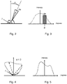
- Fig. 2 shows a schematic representation of an optoelectronic circuit having embedded optics and the ray emitted at an angle ⁇ . In Fig.
- Fig. 4 shows an example of optical functionality of an emitter circuit.
- the functionality of the optoelectronic device is determined by measuring the amount of energy emitted for each angle of emission.
- the process is initiated with a check of the behavior of the optoelectronic circuit to be encapsulated. Subsequently, all the molded layers that are going to be molded are analyzed independently in loop.
- each molded layer there are analyzed in the same measuring process the quality of the molded material, as well as the functionality of that molded layer.
- the detection of impurities, such as the bubbles and the evaluation of the birefringence is a key point and is performed by one of the measuring methods based on polariscopes, from the many described in the literature.
- the acquisition system is provided with image recognition software capable of detecting these defects and objectively evaluating the suitability of the molded material.
- the process is performed by a completely novel system with which the direction of the light emitted by the circuit and the amount of light emitted in each direction is evaluated and compared with the functionality expected from the design, being validated according to whether the result of the measured functionality is within the corresponding tolerance.
- This set-up process will depend on the end application of the optoelectronic device and the number of molded layers required for this application. Furthermore, the set-up process is taken into consideration both right at the start of the installation of the process and in subsequent readjustments thereof, since the behavior thereof may vary with the passage of time and the wear and tear of the parts of the system.
- the checking system of the process takes into consideration the option of molding various layers of plastics material by different molding technologies (injection, ultrasonic, extrusion, etc.) such that it acts sequentially on each of the layers to be molded.
- the invention also protects the instrument appropriate for performing the required measurements of the process of checking the functionality.
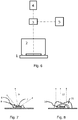
- One embodiment of this instrument shown schematically in Fig. 6 , consists of a machine having a twin arm optical system. Particularly, although without being limited to modifications in the applied technologies which do not alter the functionality of the instrument, the instrument is comprised of:
- Figs. 7 and 8 show the case of an encapsulation of two layers of plastics on an optoelectronic circuit containing a light emitting diode LED.
- the objective is to overmold the circuit with two layers of transparent plastics material which modify the original emission profile of the LED to a collimated beam emission profile.
- a start is made by obtaining an external component (namely, coming from a manufacturing method foreign to the field of the invention) such as that of Fig. 7 formed by the appropriate optoelectronic circuit containing a substrate 6, a light emitting diode 7 and connections 8 between these two components.
- This emitting diode emits rays 9 in all directions with a Lambertian emission pattern.
- Fig. 8 there is to be seen the component on which there has been overmolded a first 10 and a second 11 layers of plastics, obtaining a collimated beam of rays 12 in one same direction.
- Fig. 10 there is considered the initial optoelectronic circuit with emission of light in all directions.
- a parabolic reflector 13 By placing a parabolic reflector 13 on the sides (which is part of the aforementioned system 2), it is achieved that the light emitted up to a certain angle 14 (angle of aperture of the parabolic reflector 13) determined by the dimensions of the reflector 13 and with a preferred value of 60 degrees relative to the horizontal plane, is reflected in a vertical direction (reflected rays 15), while the remaining light exits with the original direction of emission (unreflected rays 16), preferably in a cone of light of ⁇ 30 degrees relative to the axis of emission (which, in Fig. 10 , is vertical).
- reflected rays 15 the original direction of emission
- unreflected rays 16 preferably in a cone of light of ⁇ 30 degrees relative to the axis of emission
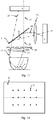
- Fig. 11 shows, in a side view of an example of the measuring equipment, the behavior of the system.
- the light emitted by the emitting diode 7 and that reflected by the parabolic reflector 13 is directed to an optical system having a convergent lens 17 and an opaque sheet 18 having a pattern of apertures (which are part also of the aforementioned system 2) and beam splitting means 3.
- the parabolic reflector 13 used has a symmetry of revolution and an aperture having a preferred dimension of 50 mm diameter.
- the convergent lens 17, having preferably a focal length of 40 mm and a diameter of 50 mm, in agreement with the aperture of the reflector 13, focuses the light coming in a vertical direction (the reflected rays 15) to a particular focal point.
- This light passes through the 1 mm diameter holes of the sheet 18 (they must not be very small to avoid diffractive patterns) preferably disposed in a square matrix spaced apart by 2 mm (for optimization of the contrast), which is behind the lens 17.
- the light emerging from the sheet enters the beam splitting means 3, with one half of the energy of the rays following the straight trajectory (convergent transmitted rays 20) towards a measuring module 4 and the other half being diverted in the perpendicular direction (convergent diverted rays 21) towards a measuring module 5.
- the convergent lens 17 is placed at the focal length of the optoelectronic circuit emitting the energy, whereby the light in the ⁇ 30 degrees range relative to the vertical plane is refracted on crossing through the lens 17, being collimated in a vertical parallel direction (according to the optical axis of the convergent lens 17, which is vertical relative to what is shown in Fig. 11 . although the whole device can have any orientation in the space).
- the measuring device 4 comprising a CCD sensor, has been placed at the focal length of the convergent lens 17, such that the light coming from the range of emission with angles greater than 30 degrees relative to the vertical plane (the convergent transmitted rays 20) are focused in the CCD sensor obtaining an image of the aperture pattern of the sheet 18, while the light coming parallel (the parallel transmitted rays 23) is not focused on the CCD sensor.
- an image of the rays emitted by the circuit in the range of angles greater than 30 degrees relative to the vertical plane namely, the axis of emission
- the measuring module 5 is comprised of a second convergent lens 25 having a short focal length, preferably 20 mm, and an image capturing CCD sensor placed in the focal plane of this second convergent lens 25.
- a second convergent lens 25 having a short focal length, preferably 20 mm
- an image capturing CCD sensor placed in the focal plane of this second convergent lens 25.
- This assembly allows us to register in a single measuring process the light emitted by thee circuit in both small and great angles of emission.
- the details of the quality of the material and the functionality may be obtained from these data as follows:
- the light may undergo variation both in the expected position and in the shape of the signal detected by the CCD sensor.
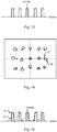
- Fig. 14 there is shown by means of circles a schematic representation of the obtained measurement 28 compared with the measurement simulated by the crosses 27.
- the variation in the position implies a variation in the directionality of the ray which implies a variation in the expected functionality of the device which may come from an irregular surface or a centring error between the lens and the optics.
- the variation in the shape of the measurement provides information on the amount of energy transmitted.
- Fig. 15 shows a schematic representation of the difference between the reading of a measurement 29 (line of dashes) and the simulated measurement 30 (continuous line). The set of the two variables of position and area under the curve allows us to validate the functionality of the device.
- Fig. 16 there is shown another embodiment of a checking device of the invention.
- the device has a parabolic reflector 13, an opaque sheet 18 with holes, a convergent lens 17 and a measuring module 4.
- the sheet 18 is disposed between the optoelectronic emitter (the diode 7) and the convergent lens 17.
- the checking device also includes a diffusor plate 31, disposed between the sheet 18 and the convergent lens 17.
- the measuring module 4 captures the image formed in the diffusor plate 31, from which the functionality of the device may be determined.
Landscapes
- Physics & Mathematics (AREA)
- General Physics & Mathematics (AREA)
- Spectroscopy & Molecular Physics (AREA)
- Led Device Packages (AREA)
- Radar Systems Or Details Thereof (AREA)
- Testing Of Optical Devices Or Fibers (AREA)
Abstract
Description
- The invention relates to a device for checking an integrated circuit having an optoelectronic emitter suitable for emitting a beam of electromagnetic radiation and defining a beam emission axis. The invention also relates to a plant for manufacturing said integrated circuits and to processes for the checking and manufacture thereof.
- Within the field of optics and, in particular, that of lenses, the checking and quality control systems in the manufacturing processes are basic and have been the object of great evolution throughout history. In general, the analysis of the manufactured lenses is divided into two large groups: mass produced lenses and the specifically manufactured lenses (or sets of lenses). Depending on which group, the quality controls are more or less exhaustive, although all of them have a common feature: these controls are always carried out in an environment and at a time isolated from the production process, whereby they cannot be considered as "on line".
- In the case of personalized, high precision lenses or sets of lenses used in image forming systems, such as may be photographic lenses, the analysis is much stricter and costly, which reflects both on the market price of the product and on the automation of the process. These exhaustive analyses are mainly carried out by methods based on the focus, contrast and other features of the image produced by the lenses or set of lenses to be analyzed.
- A particularly notable case of the image forming systems is the field of ophthalmic lenses, mass produced lenses for forming an image, but with a quality control much less strict than for other lenses. In this case, the most common thing is a random analysis of lenses normally through a process involving an observer, making it unstable and subjective. In some cases, an objective analysis is considered with some measuring device (normally based on interferometry principles) which is carried out on and validates a number of occasional measurements on selected lenses. Even so, this automatic occasional analysis does not exclude the human control relative to other qualities of the lenses. The control of these lenses is in this way due to the great optical power and versatility of the human eye, which is capable of compensating errors in the ophthalmic lenses intolerable in the case of more specialized image forming systems.
- As far as optical components directed to the field of energy transmission are concerned, for example, the field of illumination, the quality of the obtained part is not so demanding relative to the surface geometry, since it is not a so critical variant when obtaining the particular functionality, a functionality which is not checked in present day systems.
- The present invention is centred on the process for checking devices that act as encapsulated members of optoelectronic circuits. Optoelectronic circuits are those which contain members active in a particular frequency band and which interact with the exterior through windows in their encapsulation. Within these circuits there are, as the most representative, those containing light emitting diodes (LED). These devices, the applications for which are continuously on the increase, are comprised basically of a ceramic or metal plate where there are to be found the circuit connections, a die corresponding to said light emitting diode and which is usually manufactured by plating with material, the corresponding leads of gold or other metal which connect the plate to the die and the encapsulation of the component where we can find the encapsulation of the electrical circuit providing the component with protection, conductivity and heat sink properties and the encapsulation of the diode, an optical encapsulation providing the component with the adequate functionality. Up to now, the complete functionality of the LED, namely, which particular pattern of light emission the component produces, is achieved by the application of a spherical or parabolic lens over the diode (known as primary lens and manufactured by deposition of a drop of optical plastics) and a secondary lens, normally manufactured by injection of optical plastics in a different production system. This set of optics provide the component with the desired functionality. Nevertheless, it is possible to mold a number of layers of optical plastics materials over the optoelectronic circuit to provide the component with the desired functionality in the same production chain as the circuit encapsulation. The inclusion, by over-molding, of this optical component on the circuit, in a single production process, is extremely important for the reduction of associated costs and for the improvement of the component's properties, since the sources of error in the manufacture and positioning of the chips are reduced.
- Even so, within the over-molding process, since a manufacturing process of a plastics optical component is being carried out, there are a number of associated errors which can affect the behavior of the system. These errors may be both in the material, by formation, for example, of air bubbles or a compacting of non-homogenous material, in the shape of the component, by incorrect copying of the geometry of the part in the molding process, or by the relative positioning between the circuit and the optics. The combination of all these sources of error may drastically affect the functionality of the component in question. This is why there is a need for a process for checking these variables.
- There are some on-line checking methods for assembly of these components, such as, for example, the one described in
US 2014/210982 A1 by Kewei Zuo et al. , which discloses an automatic quality control method based on the automatic inspection of all the assembly steps, as well as of the end product obtained, in a feedback manner and by self-learning. Generally, the methods are focused on the evaluation of defects relating to the material and the mechanical characteristics, such as the surface of the part, but putting aside one important feature of the product, above all in the field of illumination where this invention is located: the functionality. - As far as the inspection of material is concerned, there are different variables to be taken into account and which affect the correct behavior of the device. On the one hand, the formation of bubbles in the molding process may cause a dispersion of the light which interacts negatively with the end purpose of the product. Also, the incorrect compacting of the molded material may cause an anisotropic distribution of the refractive index, creating area of birefringence, which is an indicator of internal stress of the part which may cause fracture once manufactured. In this sense, there are instruments for measuring these characteristics. In
US 5,598,262 A, Jutard et al. offer a process for the inspection of transparent material by way of the uniform illumination of the material and the analysis by contrast of the obtained transparency. By this method it is possible to detect air bubbles in the material, as well as other defects, although the measurement of birefringence is not considered. - In the case of surface inspection, the measuring methodology is broad and well-studied, although all the methods are characterized by being carried out at a time and in a space removed from the production system. This is due to the characteristic measuring times of the surfaces, too long to be performed within the production line. Furthermore, these methods are used, above all in image forming systems, where the required manufacturing accuracy is in the range of tens of nanometers, whereas in the case of energy transmission components, such as illumination, the required tolerances are to be found in the range of tens and hundreds of microns, such that the analysis of the surfaces obtained in the molding process are not so important as the other basic components, the material and the functionality.
- Nevertheless, the third of the qualities to be checked mentioned above, the functionality of the device, is not a feature where inventions or instruments are to be found, in spite of it being possibly the most important feature in the field of illumination. We can find in the state of the art inventions validating the quality of the radiation pattern of a point obtained by the reflection on a surface of a particular radiation beam such as shown by
Peter Idit in WO 2016/009440 A1 , where he measures the different characteristics of the luminous point reflected at large distances. - Considering the existing state of the art, we can see that in the field of this invention, the over-molding of optoelectronic circuits with an encapsulation having optical functionality, the existing checking systems are insufficient. either because the control is performed in an environment totally different from that of the production line, because the majority of checking systems are for the analysis of lenses having two surfaces (which is not the case presented, since there is only one interface between the plastics material and the air), because they use methods of transmission of a determined wave front (impossible to perform in the case of optics embedded in the circuit) or because they do not check the end functionality of the component.
- It is an object of the invention to overcome these drawbacks and offer a process allowing a plurality of features to be checked automatically and efficiently. This purpose is achieved by a checking device of the type indicated at the beginning, characterized in that it comprises
- electrical connecting means for connecting the optoelectronic emitter to a source of electrical energy,
- reflecting means suitable for being positioned around the optoelectronic emitter in such a way that they reflect part of the beam,
- a convergent lens the optical axis of which coincides with the axis of emission,
- an opaque sheet having a plurality of holes, and
- a measuring module suitable for receiving the electromagnetic radiation from the convergent lens.
- In fact, as will be commented upon in fuller detail hereinafter, the device of the invention allows the control of the manufactured lens to be performed on the production line itself, since it can be installed on the production line itself. Furthermore, it allows a lens embedded in a circuit to be checked, since it analyzes the light emitted (in general the electromagnetic radiation emitted) by the optoelectronic device and has no need to have access to a "front" surface of the lens nor any need for the lens to be illuminated with a particular wave front, but the light emitted by the optoelectronic device is analyzed directly. It also affords the advantage that the end functionality of the integrated circuit is analyzed directly. On the other hand, the device allows it to be totally automated.
- The checking device of the invention may be used very flexibly. Thus, it may be used only in the start-up stage of the production process, such as to allow the adjustment of the production parameters up to when the manufacturing plant is ready to start the mass production. It is also possible to use the checking device during the mass production, such that at particular times, it may be checked whether the mass production is still maintaining the initially established optimum production parameters or whether it is necessary to introduce corrections in any of the production parameters. Finally, it is possible to use the checking device to control the whole production. Therefore, it is also an object of the present invention:
- A - a checking process for an integrated circuit having an optoelectronic emitter suitable for emitting a beam of electromagnetic radiation and defining an axis of emission of the beam, characterized in that there is performed an evaluation of some real values indicative of the amount of electromagnetic radiation emitted by the optoelectronic emitter depending on the direction and it is compared with ranges of pre-set reference values where, preferably, the evaluation is performed with a checking device of the invention.
- B - a manufacturing plant for an integrated circuit having an optoelectronic emitter suitable for emitting a beam of electromagnetic radiation and defining an axis of emission of the beam, characterized in that it comprises a checking device of the invention.
- C - a manufacturing process for an integrated circuit having an optoelectronic emitter suitable for emitting a beam of electromagnetic radiation and defining an axis of emission of the beam, characterized in that it comprises a checking process of the invention. Preferably the manufacturing process comprises:
- a step of depositing a layer of polymeric material on the optoelectronic emitter.
- a checking step including the checking process of the invention,
- if the real values are outside the ranges of pre-set values, a step of adjusting at least one manufacturing parameter.
- C1- the manufacturing process preferably includes a checking step including the checking process of the invention on the optoelectronic emitter prior to the step of deposition.
- C2 -in an advantageous alternative the manufacturing process comprises a start-up step including the checking process and a mass production step not including the checking process.
- C3 - it is likewise advantageous that in the manufacturing process the integrated circuit is transported from a deposition station where the deposition step is performed to a checking station where the checking step is performed by automated transportation means,
- Preferably the checking device comprises positioning means appropriate for positioning said optoelectronic emitter such that said axis of emission coincides with said optical axis. Thus, the positioning means can take an integrated circuit from the manufacturing line, position it appropriately for performing the checking process and, as the case may be, return it to the production line after the checking process.
- Advantageously the reflecting means are a parabolic reflector. The parabolic reflector preferably has an aperture diameter of ranging from 20 to 80 mm, most preferably ranging from 47 to 53 mm. Advantageously, the ratio of the aperture diameter to the distance between the aperture and the focal point of said reflector ranges from 0.5 to 1.5.
- Preferably the reflecting means (and, in particular, the parabolic reflector) have an angle of aperture greater than 20º, preferably greater than 25º. Additionally, it is advantageous for them to have an angle of aperture smaller than 45º.
- Preferably the convergent lens has a focal length ranging from 20 to 100 mm, most preferably ranging from 37 to 43 mm. The convergent lens advantageously has an outer diameter equal to the aperture diameter of the reflecting means.
- Preferably the checking device is suitable for being disposed on the optoelectronic emitter such that the distance between the convergent lens and the optoelectronic emitter is equal to the focal length of the convergent lens.
- Advantageously the holes in the opaque sheet have such a size that the diffraction suffered by said beam may be ignored. Thus, preferably, the holes have a diameter ranging from 0.25 to 2 mm. most preferably from 0.9 to 1.1 mm. The holes are advantageously spaced apart from one another at a distance ranging from 1 to 3 mm, preferably from 1.8 to 2.2 mm.
- Preferably the measuring module comprises a CCD sensor. The measuring module is advantageously disposed at a distance from said convergent lens equal to the focal length of said convergent lens.
- In a preferred embodiment of the checking device of the invention, the convergent lens is disposed between the optoelectronic emitter and the sheet and the device comprises additionally:
- beam splitting means, disposed between the sheet and the measuring module and suitable for splitting the electromagnetic radiation from the convergent lens into a first beam propagating in a first direction and a second beam propagating in a second direction, where the first beam is directed towards the measuring module,
- a second convergent lens the optical axis of which coincides with the second direction, and
- a second measuring module suitable for receiving the electromagnetic radiation from the second convergent lens.
- In this embodiment, it is advantageous for the second convergent lens to have a focal length ranging from 10 to 50 mm, preferably ranging from 18 to 22 mm. It is also advantageous that the second measuring module should comprise a CCD sensor and/or that the second measuring module be disposed at a distance from the second convergent lens equal to the focal length of the second convergent lens.
- In a further preferred embodiment of the checking device of the invention, the sheet is disposed between the optoelectronic emitter and the convergent lens, and the device comprises, additionally, a diffusor plate disposed between the sheet and the convergent lens.
- Preferably, in the checking process of the invention, there is a step of connecting said optoelectronic emitter to a source of electrical energy, prior to the evaluation. It is likewise advantageous that prior to the evaluation there is a step of positioning reflecting means around the optoelectronic emitter. On the other hand, the evaluation advantageously comprises the comparison of the real image of each of the holes obtained in the measuring module or the second measuring module with a pre-set image. This comparison preferably includes both the comparison of the position of the real image of each of the holes of the sheet relative to some pre-set positions, and the comparison of the intensity of real radiation received in the image of each of the holes of the sheet relative to some pre-set intensities.
- Further advantages and features of the invention will become apparent from the following description, in which, without any limiting character, preferred embodiments of the invention are disclosed, with reference to the accompanying drawings in which:
-
Fig. 1 is a tree of decisions describing the setting-up process of the production line. -
Figs. 2 and 3 are a schematic representation and a graph with the variables describing the functionality of a light emitting optoelectronic circuit. -
Figs. 4 and 5 are the schematic representation and graph ofFigs. 2 and 3 applied to an example of asymmetrical distribution of intensity of a light emitting optoelectronic device. -
Fig. 6 is a schematic representation of a machine allowing the application of the invention. -
Fig. 7 is a schematic representation of an optoelectronic circuit having a light emitting diode. -
Fig. 8 is the product obtained by optical encapsulation of the optoelectronic circuit ofFig. 7 . -
Fig. 9 is a schematic representation of the checking process performed for the start-up of the manufacture of the component described inFig. 8 . -
Fig. 10 is a side view of a light emitting optoelectronic circuit with a parabolic reflector. -
Fig. 11 is a schematic representation of a possible assembly for determining the functionality of an optoelectronic circuit. -
Fig. 12 is a simulation of the image obtained by a sensor of the assembly ofFig. 11 . -
Fig. 13 is a simulation of the intensity signal obtained by the sensor ofFig. 11 in the example ofFig. 12 , -
Fig. 14 is a comparison between the simulated signal and the signal measured in the sensor of the assembly ofFig. 11 . -
Fig. 15 is a comparison between the simulated intensity signal and that obtained in the sensor ofFig. 11 in the example ofFig. 12 . -
Fig. 16 is a schematic representation of another possible assembly for determining the functionality of an optoelectronic circuit. - The present invention is based on the step by step checking of the manufacturing process of the components obtained during the start-up of the industrial process, validating the manufacturing process and the obtained component. To this end, it is necessary to check all the steps constituting the overmolding process, from the correct injection of the material by checking that no bubbles or anisotropic compactation are generated, which give rise to internal stress processes and which may end in breakage of the part, up to checking the final functionality of the component. The measurement and control of these characteristics of the product obtained during the start-up of the production system allow the set-up of the process by modifying the appropriate molding parameters. Nevertheless, the set-up of the of the production process has some very high-speed requirements, whereby there is a need for a rapid checking system integrated in the production line itself.
- The present invention presents a method of automatic inspection for the encapsulation components of optoelectronic circuits obtained by molding of plastics. In the invention the checking process of the component is considered for the set-up of the production system. To this end, a set-up process is performed in which the different steps of molding the components are sequentially analyzed with a view to providing feedback for the molding process.
Fig. 1 shows a schematic representation of the checking process for the molding of an indeterminate number of layers on a device having a particular functionality. Depending on the measurements obtained the molding parameters of these plastics layers are subjected to modification to have an adjustment of the process. This continuous adjustment process has to be performed in an environment replicating the component manufacturing conditions, whereby, considering the machines to be used (generally injectors or other molding machines having specific working conditions as far as temperature, pressure etc. are concerned, there is a need for systems allowing for a speedy measurement of the component's characteristics to be able to act as soon as possible and reduce the cost of the adjustment process to as low as possible. Thus, the proposed checking process uses novel measuring systems which provide the necessary basic information in the shortest possible time and which are easily installable in the manufacturing line. - The quality of the molding of the lens is based on the measurement and detection of possible defects such as non-homogenous bubbles or distribution of material. As far as the functionality of a light emitting device is concerned, this is described in the directionality of the light emitted and the amount of light emitted in each direction. Commonly, to describe these variables, emission graphs are used where on the X-axis there are shown the degrees of light emission and on the Y-axis the emitted intensity (usually standardized.
Fig. 2 shows a schematic representation of an optoelectronic circuit having embedded optics and the ray emitted at an angle θ. InFig. 3 there is shown a corresponding graph in which the energy emitted around this angle, with standardized energy values, is shown on the Y-axis, as function of the degree θ.Fig. 4 shows an example of optical functionality of an emitter circuit. In this case, it can be seen that the emission lobe is not symmetrical relative to the emission angle θ=0 and that there is a greater amount of energy emitted in the negative angle values than in the positive ones, such as shown in the graph ofFig. 5 . Thus, the functionality of the optoelectronic device is determined by measuring the amount of energy emitted for each angle of emission. - The process is initiated with a check of the behavior of the optoelectronic circuit to be encapsulated. Subsequently, all the molded layers that are going to be molded are analyzed independently in loop.
- For the analysis of each molded layer, there are analyzed in the same measuring process the quality of the molded material, as well as the functionality of that molded layer. As far as the quality of the material is concerned, the detection of impurities, such as the bubbles and the evaluation of the birefringence is a key point and is performed by one of the measuring methods based on polariscopes, from the many described in the literature. The acquisition system is provided with image recognition software capable of detecting these defects and objectively evaluating the suitability of the molded material. Although the quality of the molded material depends on many factors, these processes of creation of defects in the material are very closely related to the melting point of the material and the properties thereof on flowing, whereby, among other characteristics, the control and adjustment of the temperature cycles of the molding process is very important for readjusting the behavior of the machine iteratively until the validation is achieved.
- Concerning the evaluation of the functionality of the component formed by the optoelectronic circuit and the corresponding molded layer in which it is found, the process is performed by a completely novel system with which the direction of the light emitted by the circuit and the amount of light emitted in each direction is evaluated and compared with the functionality expected from the design, being validated according to whether the result of the measured functionality is within the corresponding tolerance.
- This set-up process will depend on the end application of the optoelectronic device and the number of molded layers required for this application. Furthermore, the set-up process is taken into consideration both right at the start of the installation of the process and in subsequent readjustments thereof, since the behavior thereof may vary with the passage of time and the wear and tear of the parts of the system.
- The checking system of the process takes into consideration the option of molding various layers of plastics material by different molding technologies (injection, ultrasonic, extrusion, etc.) such that it acts sequentially on each of the layers to be molded.
- The invention also protects the instrument appropriate for performing the required measurements of the process of checking the functionality. One embodiment of this instrument, shown schematically in
Fig. 6 , consists of a machine having a twin arm optical system. Particularly, although without being limited to modifications in the applied technologies which do not alter the functionality of the instrument, the instrument is comprised of: - positioning means 1 automated in the production line housing the optoelectronic circuit and the molded layer,
- a system 2 allowing the disposal of different optical and mechanical members on the optoelectronic circuit,
- beam splitting means 3 allowing the light emitted by the optoelectronic member to be split according to the axis of emission, which allows the application of two optical systems with two measuring
modules -
Figs. 7 and 8 show the case of an encapsulation of two layers of plastics on an optoelectronic circuit containing a light emitting diode LED. The objective is to overmold the circuit with two layers of transparent plastics material which modify the original emission profile of the LED to a collimated beam emission profile. In the initial state of the process, a start is made by obtaining an external component (namely, coming from a manufacturing method foreign to the field of the invention) such as that ofFig. 7 formed by the appropriate optoelectronic circuit containing asubstrate 6, alight emitting diode 7 andconnections 8 between these two components. This emitting diode emits rays 9 in all directions with a Lambertian emission pattern. The purpose of the manufacturing process is to encapsulate this circuit by way of two molded layers of transparent plastics and conforming a collimation if the emitted rays. InFig. 8 there is to be seen the component on which there has been overmolded a first 10 and a second 11 layers of plastics, obtaining a collimated beam ofrays 12 in one same direction. - To perform the checking process of this device, the layout of
Fig. 1 is followed, bearing in mind that the number of layers to be molded is two. Thus, the manufacturing adjustment process, schematically shown inFig. 9 , is as follows: - S1 Initial circuit analysis;
- 1.1. Receipt of the optoelectronic circuit having the LED.
- 1.2 Measurement of the emission pattern of the LED. this step is important since the design of the geometrical forms of the optical components depends a lot on the source of emission and it must be checked that the real emission pattern is the same as the one used when carrying out the optical design of the component.
- S2 Analysis of the first molded layer.
- 2.1. Overmolding of the first geometrical form on the corresponding optoelectronic circuit.
- 2.2. Measurement of the properties of the molded material.
- 2.2.1. If necessary, readjustment of the molding conditions and return to point 2.1 of the process.
- 2.2.2. If the properties of the material are correct, move on to step 2.3.
- 2.3. Measurement of the functionality of the obtained ensemble.
- 2.3.1. If necessary, readjustment of the molding conditions and return to point 2.1 of the process.
- 2.3.2. If the properties of the material are correct, move on to point 2.4
- 2.4. The molding parameters obtained are established as the appropriate ones for this first layer of the component.
- S3 Analysis of the second molded layer.
- 3.1. Overmolding of the second geometrical form on the corresponding optoelectronic circuit and first molded layer.
- 3.2. Measurement of the properties of the molded material.
- 3.2.1. If necessary, readjustment of the molding conditions and return to point 3.1 of the process.
- 3.2.2. If the properties of the material are correct, move on to point 3.3.
- 3.3. Measurement of the functionality of the obtained ensemble.
- 3.3.1. If necessary, readjustment of the molding conditions and return to point 3.1 of the process.
- 3.3.2. If the properties of the material are correct, move on to point 3.4
- 3.4. The molding parameters obtained are established as the appropriate ones for this second component.
- S4 End of the adjustment process.
- Within the checking process the quality parameters governing the acceptance of the parts at the different points are taken into account. These parameters will depend on the end application to which the component is destined.
- As far as the measurement of the functionality of the molded layer is concerned, they are performed, for example, with the following process and assembly.
- In
Fig. 10 there is considered the initial optoelectronic circuit with emission of light in all directions. By placing aparabolic reflector 13 on the sides (which is part of the aforementioned system 2), it is achieved that the light emitted up to a certain angle 14 (angle of aperture of the parabolic reflector 13) determined by the dimensions of thereflector 13 and with a preferred value of 60 degrees relative to the horizontal plane, is reflected in a vertical direction (reflected rays 15), while the remaining light exits with the original direction of emission (unreflected rays 16), preferably in a cone of light of ± 30 degrees relative to the axis of emission (which, inFig. 10 , is vertical). Thus, there is achieved a modification of the direction of the rays emitted at the angles greater than the angle ofaperture 14 and the concentration thereof within the optical system which will be used. -
Fig. 11 shows, in a side view of an example of the measuring equipment, the behavior of the system. The light emitted by the emittingdiode 7 and that reflected by theparabolic reflector 13 is directed to an optical system having aconvergent lens 17 and anopaque sheet 18 having a pattern of apertures (which are part also of the aforementioned system 2) and beam splitting means 3. Theparabolic reflector 13 used has a symmetry of revolution and an aperture having a preferred dimension of 50 mm diameter. - The
convergent lens 17, having preferably a focal length of 40 mm and a diameter of 50 mm, in agreement with the aperture of thereflector 13, focuses the light coming in a vertical direction (the reflected rays 15) to a particular focal point. This light passes through the 1 mm diameter holes of the sheet 18 (they must not be very small to avoid diffractive patterns) preferably disposed in a square matrix spaced apart by 2 mm (for optimization of the contrast), which is behind thelens 17. The light emerging from the sheet enters the beam splitting means 3, with one half of the energy of the rays following the straight trajectory (convergent transmitted rays 20) towards a measuringmodule 4 and the other half being diverted in the perpendicular direction (convergent diverted rays 21) towards a measuringmodule 5. On the other hand, theconvergent lens 17 is placed at the focal length of the optoelectronic circuit emitting the energy, whereby the light in the ± 30 degrees range relative to the vertical plane is refracted on crossing through thelens 17, being collimated in a vertical parallel direction (according to the optical axis of theconvergent lens 17, which is vertical relative to what is shown inFig. 11 . although the whole device can have any orientation in the space). They are theparallel rays 22. This light is subjected to the same effect as the previous light on crossing through the beam splitting means 3: one half of the light is transmitted (parallel transmitted rays 23) towards the measuringmodule 4 and the other half (parallel diverted rays 24) is reflected towards the measuringmodule 5. - The measuring
device 4, comprising a CCD sensor, has been placed at the focal length of theconvergent lens 17, such that the light coming from the range of emission with angles greater than 30 degrees relative to the vertical plane (the convergent transmitted rays 20) are focused in the CCD sensor obtaining an image of the aperture pattern of thesheet 18, while the light coming parallel (the parallel transmitted rays 23) is not focused on the CCD sensor. Thus, an image of the rays emitted by the circuit in the range of angles greater than 30 degrees relative to the vertical plane (namely, the axis of emission) is collected in the sensor of themeasuring module 4. - The measuring
module 5 is comprised of a secondconvergent lens 25 having a short focal length, preferably 20 mm, and an image capturing CCD sensor placed in the focal plane of this secondconvergent lens 25. Thus, the light coming collimated from the beam splitting means 3 (the parallel diverted rays 24) will be focused, projected and registered in the CCD sensor, while the light coming converging from the convergent lens 17 (the convergent diverted rays 21) will not be focused on this CCD sensor. Thus, only the rays emitted by the circuit in the range of angles smaller than 30 degrees relative to the vertical plane will be collected in themeasuring module 5. - This assembly allows us to register in a single measuring process the light emitted by thee circuit in both small and great angles of emission. The details of the quality of the material and the functionality may be obtained from these data as follows:
- bearing in mind the emission pattern expected by the initial circuit, the surfaces molded on the circuit (considering according to the point of the process at which we are one molded layer, various, or all) and the optical components used in the assembly, simulations of the expected measurement may be made both for the
measuring module 4 and for themeasuring module 5. The theoretical measuring point to be registered has a position in the sensor determined by the location of the aperture of the sheet through which the light passes, whereby if we consider a rectangular matrix of aperture in thesheet 18, the image expected in the CCD sensors is an approximately rectangular matrix.Fig. 12 shows a scheme of the image expected in aCCD sensor 26 where each of thecrosses 27 marks the expected position of each ray. Each of these points in the simulated system must have an intensity like that schematically shown inFig. 13 , the height and width of which will depend on the position and the amount of energy expected. The location of this signal on the CCD sensor therefore marks the directionality of the analyzed ray as well as the energy flow transmitted, this being the area under the simulated curve ofFig. 13 . - In the case of a real measurement, the light may undergo variation both in the expected position and in the shape of the signal detected by the CCD sensor. In
Fig. 14 there is shown by means of circles a schematic representation of the obtainedmeasurement 28 compared with the measurement simulated by thecrosses 27. The variation in the position implies a variation in the directionality of the ray which implies a variation in the expected functionality of the device which may come from an irregular surface or a centring error between the lens and the optics. On the other hand, the variation in the shape of the measurement provides information on the amount of energy transmitted.Fig. 15 shows a schematic representation of the difference between the reading of a measurement 29 (line of dashes) and the simulated measurement 30 (continuous line). The set of the two variables of position and area under the curve allows us to validate the functionality of the device. - In
Fig. 16 there is shown another embodiment of a checking device of the invention. In this case the device has aparabolic reflector 13, anopaque sheet 18 with holes, aconvergent lens 17 and ameasuring module 4. In this embodiment, thesheet 18 is disposed between the optoelectronic emitter (the diode 7) and theconvergent lens 17. The checking device also includes adiffusor plate 31, disposed between thesheet 18 and theconvergent lens 17. The measuringmodule 4 captures the image formed in thediffusor plate 31, from which the functionality of the device may be determined.
Claims (17)
- A device for checking an integrated circuit having an optoelectronic emitter suitable for emitting a beam of electromagnetic radiation and defining an axis of emission of said beam, characterized in that it comprises:- electrical connecting means for connecting said optoelectronic emitter to a source of electrical energy,- reflecting means (13) suitable for being positioned around said optoelectronic emitter in such a way that they reflect part of said beam,- a convergent lens (17) the optical axis of which coincides with said axis of emission,- an opaque sheet (18) having a plurality of holes, and- a measuring module (4) suitable for receiving the electromagnetic radiation coming from the convergent lens (17).
- A device according to claim 1, characterized in that said reflecting means (13) are a parabolic reflector preferably having an aperture diameter ranging from 20 to 80 mm, and most preferably ranging from 47 to 53 mm.
- A device according to claim 2, characterized in that the ratio of the aperture diameter to the distance between the aperture and the focal point of said reflector ranges from 0.5 to 1.5.
- A device according to any one of claims 1 to 3, characterized in that said reflecting means (13) have an angle of aperture greater than 20º, preferably greater than 25º.
- A device according to any one of claims 1 to 4, characterized in that said reflecting means (13) have an angle of aperture smaller than 45°.
- A device according to any one of claims 1 to 5, characterized in that said convergent lens (17) has a focal length ranging from 20 to 100 mm, preferably ranging from 37 to 43 mm.
- A device according to any one of claims 1 to 6, characterized in that said holes have a diameter ranging from 0.25 to 2 mm, preferably from 0.9 to 1.1 mm.
- A device according to any one of claims 1 to 7, characterized in that said holes are spaced apart from one another at a distance ranging from 1 to 3 mm, preferably from 1.8 to 2.2 mm.
- A device according to any one of claims 1 to 8, characterized in that said convergent lens (17) is disposed between said optoelectronic emitter and said sheet (18) and said device comprises additionally:- beam splitting means (3), disposed between said sheet (18) and said measuring module (4) and suitable for splitting the electromagnetic radiation coming from said convergent lens (17) into a first beam (20, 23) propagating in a first direction and a second beam (21, 24) propagating in a second direction, where said first beam is directed towards said measuring module (4),- a second convergent lens (25) the optical axis of which coincides with said second direction, and- a second measuring module (5) suitable for receiving the electromagnetic radiation coming from said second convergent lens (25).
- A device according to claim 9, characterized in that said second convergent lens (25) has a focal length ranging from 10 to 50 mm, preferably ranging from 18 to 22 mm.
- A device according to any one of claims 1 to 8, characterized in that said sheet (18) is disposed between said optoelectronic emitter and said convergent lens (17), and said device comprises, additionally, a diffusor plate (31) disposed between said sheet (18) and said convergent lens (17).
- A plant for the manufacture of an integrated circuit having an optoelectronic emitter suitable for emitting a beam of electromagnetic radiation and defining an axis of emission of said beam, characterized in that it comprises a checking device according to any one of claims 1 to 11.
- A process for checking an integrated circuit having an optoelectronic emitter suitable for emitting a beam of electromagnetic radiation and defining an axis of emission of said beam, characterized in that there is performed an evaluation of some real values indicative of the amount of electromagnetic radiation emitted by said optoelectronic emitter depending on the direction and it is compared with some ranges of pre-set reference values.
- A process according to claim 13, characterized in that said evaluation is performed with a device according to any one of claims 1 to 11.
- A process according to one of claims 13 or 14, characterized in that said evaluation comprises the comparison of the real image of each of said holes obtained in the measuring module or the second measuring module with a pre-set image where, preferably, said comparison includes both the comparison of the position of the real image of each of said holes of the sheet relative to some pre-set positions, and the comparison of the intensity of real radiation received in the image of each of the holes of said sheet relative to some pre-set intensities.
- A process for manufacturing an integrated circuit having an optoelectronic emitter suitable for emitting a beam of electromagnetic radiation and defining an axis of emission of said beam, characterized in that it comprises a checking process according to any one of claims 13 to 15.
- A process according to claim 16, characterized in that it comprises:- a step of depositing a layer of polymeric material on said optoelectronic emitter.- a checking step including said checking process, and- if said real values are outside said ranges of pre-set values, a step of adjusting at least one manufacturing parameter.
Priority Applications (2)
| Application Number | Priority Date | Filing Date | Title |
|---|---|---|---|
| EP18382831.8A EP3657535B1 (en) | 2018-11-20 | 2018-11-20 | Device for testing an integrated circuit with optoelectronic emitter, manufacturing system and associated testing and manufacturing process |
| ES18382831T ES2942576T3 (en) | 2018-11-20 | 2018-11-20 | Verification device for an integrated circuit with an optoelectronic transmitter, manufacturing system and associated verification and manufacturing process |
Applications Claiming Priority (1)
| Application Number | Priority Date | Filing Date | Title |
|---|---|---|---|
| EP18382831.8A EP3657535B1 (en) | 2018-11-20 | 2018-11-20 | Device for testing an integrated circuit with optoelectronic emitter, manufacturing system and associated testing and manufacturing process |
Publications (2)
| Publication Number | Publication Date |
|---|---|
| EP3657535A1 true EP3657535A1 (en) | 2020-05-27 |
| EP3657535B1 EP3657535B1 (en) | 2023-02-15 |
Family
ID=64949126
Family Applications (1)
| Application Number | Title | Priority Date | Filing Date |
|---|---|---|---|
| EP18382831.8A Active EP3657535B1 (en) | 2018-11-20 | 2018-11-20 | Device for testing an integrated circuit with optoelectronic emitter, manufacturing system and associated testing and manufacturing process |
Country Status (2)
| Country | Link |
|---|---|
| EP (1) | EP3657535B1 (en) |
| ES (1) | ES2942576T3 (en) |
Citations (8)
| Publication number | Priority date | Publication date | Assignee | Title |
|---|---|---|---|---|
| US5598262A (en) | 1992-10-20 | 1997-01-28 | Thomson-Csf | Process and device for inspecting transparent material |
| JP2010286339A (en) * | 2009-06-11 | 2010-12-24 | Rozefu Technol:Kk | Method of inspecting directivity of light source and apparatus therefor |
| US20110241549A1 (en) * | 2010-03-31 | 2011-10-06 | Ats Automation Tooling Systems Inc. | Light generator systems and methods |
| CN102735424A (en) * | 2011-04-02 | 2012-10-17 | 浙江天时光电科技有限公司 | Led lamp light distribution tester |
| KR101291914B1 (en) * | 2012-11-08 | 2013-07-31 | 서승환 | Method for light emitting module's optical axis measuring |
| US20140210982A1 (en) | 2013-01-30 | 2014-07-31 | Taiwan Semiconductor Manufacturing Co., Ltd. | System and method for automatic quality control for assembly line processes |
| US20150369695A1 (en) * | 2014-06-20 | 2015-12-24 | National Central University | Detecting system |
| WO2016009440A1 (en) | 2014-07-17 | 2016-01-21 | Elbit Systems Electro-Optics Elop Ltd. | System and method for analyzing quality criteria of a radiation spot |
-
2018
- 2018-11-20 ES ES18382831T patent/ES2942576T3/en active Active
- 2018-11-20 EP EP18382831.8A patent/EP3657535B1/en active Active
Patent Citations (8)
| Publication number | Priority date | Publication date | Assignee | Title |
|---|---|---|---|---|
| US5598262A (en) | 1992-10-20 | 1997-01-28 | Thomson-Csf | Process and device for inspecting transparent material |
| JP2010286339A (en) * | 2009-06-11 | 2010-12-24 | Rozefu Technol:Kk | Method of inspecting directivity of light source and apparatus therefor |
| US20110241549A1 (en) * | 2010-03-31 | 2011-10-06 | Ats Automation Tooling Systems Inc. | Light generator systems and methods |
| CN102735424A (en) * | 2011-04-02 | 2012-10-17 | 浙江天时光电科技有限公司 | Led lamp light distribution tester |
| KR101291914B1 (en) * | 2012-11-08 | 2013-07-31 | 서승환 | Method for light emitting module's optical axis measuring |
| US20140210982A1 (en) | 2013-01-30 | 2014-07-31 | Taiwan Semiconductor Manufacturing Co., Ltd. | System and method for automatic quality control for assembly line processes |
| US20150369695A1 (en) * | 2014-06-20 | 2015-12-24 | National Central University | Detecting system |
| WO2016009440A1 (en) | 2014-07-17 | 2016-01-21 | Elbit Systems Electro-Optics Elop Ltd. | System and method for analyzing quality criteria of a radiation spot |
Also Published As
| Publication number | Publication date |
|---|---|
| EP3657535B1 (en) | 2023-02-15 |
| ES2942576T3 (en) | 2023-06-02 |
Similar Documents
| Publication | Publication Date | Title |
|---|---|---|
| TWI480501B (en) | Displacement measurement method and displacement measuring device | |
| US7862207B2 (en) | Optimizing use and performance of optical systems implemented with telecentric on-axis dark field illumination | |
| US7655896B2 (en) | Optical sensor, method for producing an optical sensor, and method for detecting an object with an optical sensor | |
| CN102822656B (en) | Offset measuring method | |
| CN105509639A (en) | Measuring system and measuring method for measuring geometrical characteristics | |
| JPH0355501A (en) | Lens array plate | |
| US6710286B2 (en) | Chip scale marker and making method | |
| EP3657535B1 (en) | Device for testing an integrated circuit with optoelectronic emitter, manufacturing system and associated testing and manufacturing process | |
| Loaldi et al. | Tolerance verification of precision injection moulded Fresnel lenses | |
| US12242246B2 (en) | Method and system of operating overlay measuring | |
| NL8103462A (en) | DEVICE FOR OPTICAL SCANNING. | |
| CN103383469B (en) | For the lens mount of light curtain and optical module and processing method | |
| KR101612276B1 (en) | Condensing device for lighting and manufacture method thereof | |
| KR20060131721A (en) | Lighting unit with light conductor and integrated optical lens | |
| US20230273530A1 (en) | Overlay measuring apparatus | |
| JP2003050109A (en) | Surface shape measuring device and surface shape measuring method | |
| JP6821402B2 (en) | Optical parts, injection molding dies for optical parts, and injection molding methods for optical parts | |
| US20240027656A1 (en) | Diffuser, light-emitting device, and sensor module | |
| Keränen et al. | Injection moulding integration of a red VCSEL illuminator module for a hologram reader sensor | |
| JP5359468B2 (en) | Lens molding die, lens molding apparatus, and lens | |
| JP2020024284A (en) | Diffraction optical element, multifaceted body, inspection method of multifaceted body, light irradiation device, adjustment method of light irradiation device | |
| CN121141700B (en) | A laser-based weld quality inspection system and method | |
| CN120807473B (en) | Defect detection method and system for atmosphere lamp | |
| CN110837139B (en) | Optical lenses for devices equipped with photodiodes | |
| KR20130013439A (en) | Lens imprinting device and lens imprinting method including the saem |
Legal Events
| Date | Code | Title | Description |
|---|---|---|---|
| PUAI | Public reference made under article 153(3) epc to a published international application that has entered the european phase |
Free format text: ORIGINAL CODE: 0009012 |
|
| STAA | Information on the status of an ep patent application or granted ep patent |
Free format text: STATUS: THE APPLICATION HAS BEEN PUBLISHED |
|
| AK | Designated contracting states |
Kind code of ref document: A1 Designated state(s): AL AT BE BG CH CY CZ DE DK EE ES FI FR GB GR HR HU IE IS IT LI LT LU LV MC MK MT NL NO PL PT RO RS SE SI SK SM TR |
|
| AX | Request for extension of the european patent |
Extension state: BA ME |
|
| STAA | Information on the status of an ep patent application or granted ep patent |
Free format text: STATUS: REQUEST FOR EXAMINATION WAS MADE |
|
| 17P | Request for examination filed |
Effective date: 20201126 |
|
| RBV | Designated contracting states (corrected) |
Designated state(s): AL AT BE BG CH CY CZ DE DK EE ES FI FR GB GR HR HU IE IS IT LI LT LU LV MC MK MT NL NO PL PT RO RS SE SI SK SM TR |
|
| RIC1 | Information provided on ipc code assigned before grant |
Ipc: G01N 21/88 20060101ALI20211119BHEP Ipc: G01N 21/958 20060101ALI20211119BHEP Ipc: G01J 1/02 20060101ALI20211119BHEP Ipc: G01J 1/04 20060101ALI20211119BHEP Ipc: G01J 1/42 20060101ALI20211119BHEP Ipc: H01L 21/66 20060101AFI20211119BHEP |
|
| GRAP | Despatch of communication of intention to grant a patent |
Free format text: ORIGINAL CODE: EPIDOSNIGR1 |
|
| STAA | Information on the status of an ep patent application or granted ep patent |
Free format text: STATUS: GRANT OF PATENT IS INTENDED |
|
| INTG | Intention to grant announced |
Effective date: 20220216 |
|
| GRAJ | Information related to disapproval of communication of intention to grant by the applicant or resumption of examination proceedings by the epo deleted |
Free format text: ORIGINAL CODE: EPIDOSDIGR1 |
|
| STAA | Information on the status of an ep patent application or granted ep patent |
Free format text: STATUS: REQUEST FOR EXAMINATION WAS MADE |
|
| INTC | Intention to grant announced (deleted) | ||
| GRAP | Despatch of communication of intention to grant a patent |
Free format text: ORIGINAL CODE: EPIDOSNIGR1 |
|
| STAA | Information on the status of an ep patent application or granted ep patent |
Free format text: STATUS: GRANT OF PATENT IS INTENDED |
|
| INTG | Intention to grant announced |
Effective date: 20220912 |
|
| GRAS | Grant fee paid |
Free format text: ORIGINAL CODE: EPIDOSNIGR3 |
|
| GRAA | (expected) grant |
Free format text: ORIGINAL CODE: 0009210 |
|
| STAA | Information on the status of an ep patent application or granted ep patent |
Free format text: STATUS: THE PATENT HAS BEEN GRANTED |
|
| AK | Designated contracting states |
Kind code of ref document: B1 Designated state(s): AL AT BE BG CH CY CZ DE DK EE ES FI FR GB GR HR HU IE IS IT LI LT LU LV MC MK MT NL NO PL PT RO RS SE SI SK SM TR |
|
| REG | Reference to a national code |
Ref country code: CH Ref legal event code: EP Ref country code: GB Ref legal event code: FG4D |
|
| REG | Reference to a national code |
Ref country code: DE Ref legal event code: R096 Ref document number: 602018046124 Country of ref document: DE |
|
| REG | Reference to a national code |
Ref country code: AT Ref legal event code: REF Ref document number: 1548674 Country of ref document: AT Kind code of ref document: T Effective date: 20230315 Ref country code: IE Ref legal event code: FG4D |
|
| REG | Reference to a national code |
Ref country code: ES Ref legal event code: FG2A Ref document number: 2942576 Country of ref document: ES Kind code of ref document: T3 Effective date: 20230602 |
|
| REG | Reference to a national code |
Ref country code: LT Ref legal event code: MG9D |
|
| REG | Reference to a national code |
Ref country code: NL Ref legal event code: MP Effective date: 20230215 |
|
| REG | Reference to a national code |
Ref country code: AT Ref legal event code: MK05 Ref document number: 1548674 Country of ref document: AT Kind code of ref document: T Effective date: 20230215 |
|
| PG25 | Lapsed in a contracting state [announced via postgrant information from national office to epo] |
Ref country code: RS Free format text: LAPSE BECAUSE OF FAILURE TO SUBMIT A TRANSLATION OF THE DESCRIPTION OR TO PAY THE FEE WITHIN THE PRESCRIBED TIME-LIMIT Effective date: 20230215 Ref country code: PT Free format text: LAPSE BECAUSE OF FAILURE TO SUBMIT A TRANSLATION OF THE DESCRIPTION OR TO PAY THE FEE WITHIN THE PRESCRIBED TIME-LIMIT Effective date: 20230615 Ref country code: NO Free format text: LAPSE BECAUSE OF FAILURE TO SUBMIT A TRANSLATION OF THE DESCRIPTION OR TO PAY THE FEE WITHIN THE PRESCRIBED TIME-LIMIT Effective date: 20230515 Ref country code: NL Free format text: LAPSE BECAUSE OF FAILURE TO SUBMIT A TRANSLATION OF THE DESCRIPTION OR TO PAY THE FEE WITHIN THE PRESCRIBED TIME-LIMIT Effective date: 20230215 Ref country code: LV Free format text: LAPSE BECAUSE OF FAILURE TO SUBMIT A TRANSLATION OF THE DESCRIPTION OR TO PAY THE FEE WITHIN THE PRESCRIBED TIME-LIMIT Effective date: 20230215 Ref country code: LT Free format text: LAPSE BECAUSE OF FAILURE TO SUBMIT A TRANSLATION OF THE DESCRIPTION OR TO PAY THE FEE WITHIN THE PRESCRIBED TIME-LIMIT Effective date: 20230215 Ref country code: HR Free format text: LAPSE BECAUSE OF FAILURE TO SUBMIT A TRANSLATION OF THE DESCRIPTION OR TO PAY THE FEE WITHIN THE PRESCRIBED TIME-LIMIT Effective date: 20230215 Ref country code: AT Free format text: LAPSE BECAUSE OF FAILURE TO SUBMIT A TRANSLATION OF THE DESCRIPTION OR TO PAY THE FEE WITHIN THE PRESCRIBED TIME-LIMIT Effective date: 20230215 |
|
| PG25 | Lapsed in a contracting state [announced via postgrant information from national office to epo] |
Ref country code: SE Free format text: LAPSE BECAUSE OF FAILURE TO SUBMIT A TRANSLATION OF THE DESCRIPTION OR TO PAY THE FEE WITHIN THE PRESCRIBED TIME-LIMIT Effective date: 20230215 Ref country code: PL Free format text: LAPSE BECAUSE OF FAILURE TO SUBMIT A TRANSLATION OF THE DESCRIPTION OR TO PAY THE FEE WITHIN THE PRESCRIBED TIME-LIMIT Effective date: 20230215 Ref country code: IS Free format text: LAPSE BECAUSE OF FAILURE TO SUBMIT A TRANSLATION OF THE DESCRIPTION OR TO PAY THE FEE WITHIN THE PRESCRIBED TIME-LIMIT Effective date: 20230615 Ref country code: GR Free format text: LAPSE BECAUSE OF FAILURE TO SUBMIT A TRANSLATION OF THE DESCRIPTION OR TO PAY THE FEE WITHIN THE PRESCRIBED TIME-LIMIT Effective date: 20230516 Ref country code: FI Free format text: LAPSE BECAUSE OF FAILURE TO SUBMIT A TRANSLATION OF THE DESCRIPTION OR TO PAY THE FEE WITHIN THE PRESCRIBED TIME-LIMIT Effective date: 20230215 |
|
| PG25 | Lapsed in a contracting state [announced via postgrant information from national office to epo] |
Ref country code: SM Free format text: LAPSE BECAUSE OF FAILURE TO SUBMIT A TRANSLATION OF THE DESCRIPTION OR TO PAY THE FEE WITHIN THE PRESCRIBED TIME-LIMIT Effective date: 20230215 Ref country code: RO Free format text: LAPSE BECAUSE OF FAILURE TO SUBMIT A TRANSLATION OF THE DESCRIPTION OR TO PAY THE FEE WITHIN THE PRESCRIBED TIME-LIMIT Effective date: 20230215 Ref country code: EE Free format text: LAPSE BECAUSE OF FAILURE TO SUBMIT A TRANSLATION OF THE DESCRIPTION OR TO PAY THE FEE WITHIN THE PRESCRIBED TIME-LIMIT Effective date: 20230215 Ref country code: DK Free format text: LAPSE BECAUSE OF FAILURE TO SUBMIT A TRANSLATION OF THE DESCRIPTION OR TO PAY THE FEE WITHIN THE PRESCRIBED TIME-LIMIT Effective date: 20230215 Ref country code: CZ Free format text: LAPSE BECAUSE OF FAILURE TO SUBMIT A TRANSLATION OF THE DESCRIPTION OR TO PAY THE FEE WITHIN THE PRESCRIBED TIME-LIMIT Effective date: 20230215 |
|
| REG | Reference to a national code |
Ref country code: DE Ref legal event code: R097 Ref document number: 602018046124 Country of ref document: DE |
|
| PG25 | Lapsed in a contracting state [announced via postgrant information from national office to epo] |
Ref country code: SK Free format text: LAPSE BECAUSE OF FAILURE TO SUBMIT A TRANSLATION OF THE DESCRIPTION OR TO PAY THE FEE WITHIN THE PRESCRIBED TIME-LIMIT Effective date: 20230215 |
|
| PLBE | No opposition filed within time limit |
Free format text: ORIGINAL CODE: 0009261 |
|
| STAA | Information on the status of an ep patent application or granted ep patent |
Free format text: STATUS: NO OPPOSITION FILED WITHIN TIME LIMIT |
|
| 26N | No opposition filed |
Effective date: 20231116 |
|
| PG25 | Lapsed in a contracting state [announced via postgrant information from national office to epo] |
Ref country code: SI Free format text: LAPSE BECAUSE OF FAILURE TO SUBMIT A TRANSLATION OF THE DESCRIPTION OR TO PAY THE FEE WITHIN THE PRESCRIBED TIME-LIMIT Effective date: 20230215 |
|
| PG25 | Lapsed in a contracting state [announced via postgrant information from national office to epo] |
Ref country code: IT Free format text: LAPSE BECAUSE OF FAILURE TO SUBMIT A TRANSLATION OF THE DESCRIPTION OR TO PAY THE FEE WITHIN THE PRESCRIBED TIME-LIMIT Effective date: 20230215 |
|
| REG | Reference to a national code |
Ref country code: CH Ref legal event code: PL |
|
| PG25 | Lapsed in a contracting state [announced via postgrant information from national office to epo] |
Ref country code: MC Free format text: LAPSE BECAUSE OF FAILURE TO SUBMIT A TRANSLATION OF THE DESCRIPTION OR TO PAY THE FEE WITHIN THE PRESCRIBED TIME-LIMIT Effective date: 20230215 |
|
| PG25 | Lapsed in a contracting state [announced via postgrant information from national office to epo] |
Ref country code: LU Free format text: LAPSE BECAUSE OF NON-PAYMENT OF DUE FEES Effective date: 20231120 |
|
| PG25 | Lapsed in a contracting state [announced via postgrant information from national office to epo] |
Ref country code: CH Free format text: LAPSE BECAUSE OF NON-PAYMENT OF DUE FEES Effective date: 20231130 |
|
| GBPC | Gb: european patent ceased through non-payment of renewal fee |
Effective date: 20231120 |
|
| PG25 | Lapsed in a contracting state [announced via postgrant information from national office to epo] |
Ref country code: MC Free format text: LAPSE BECAUSE OF FAILURE TO SUBMIT A TRANSLATION OF THE DESCRIPTION OR TO PAY THE FEE WITHIN THE PRESCRIBED TIME-LIMIT Effective date: 20230215 Ref country code: LU Free format text: LAPSE BECAUSE OF NON-PAYMENT OF DUE FEES Effective date: 20231120 Ref country code: CH Free format text: LAPSE BECAUSE OF NON-PAYMENT OF DUE FEES Effective date: 20231130 |
|
| REG | Reference to a national code |
Ref country code: BE Ref legal event code: MM Effective date: 20231130 |
|
| REG | Reference to a national code |
Ref country code: IE Ref legal event code: MM4A |
|
| PG25 | Lapsed in a contracting state [announced via postgrant information from national office to epo] |
Ref country code: IE Free format text: LAPSE BECAUSE OF NON-PAYMENT OF DUE FEES Effective date: 20231120 |
|
| PG25 | Lapsed in a contracting state [announced via postgrant information from national office to epo] |
Ref country code: GB Free format text: LAPSE BECAUSE OF NON-PAYMENT OF DUE FEES Effective date: 20231120 |
|
| PG25 | Lapsed in a contracting state [announced via postgrant information from national office to epo] |
Ref country code: BE Free format text: LAPSE BECAUSE OF NON-PAYMENT OF DUE FEES Effective date: 20231130 |
|
| PG25 | Lapsed in a contracting state [announced via postgrant information from national office to epo] |
Ref country code: FR Free format text: LAPSE BECAUSE OF NON-PAYMENT OF DUE FEES Effective date: 20231130 |
|
| PG25 | Lapsed in a contracting state [announced via postgrant information from national office to epo] |
Ref country code: IE Free format text: LAPSE BECAUSE OF NON-PAYMENT OF DUE FEES Effective date: 20231120 Ref country code: GB Free format text: LAPSE BECAUSE OF NON-PAYMENT OF DUE FEES Effective date: 20231120 Ref country code: FR Free format text: LAPSE BECAUSE OF NON-PAYMENT OF DUE FEES Effective date: 20231130 Ref country code: BE Free format text: LAPSE BECAUSE OF NON-PAYMENT OF DUE FEES Effective date: 20231130 |
|
| PG25 | Lapsed in a contracting state [announced via postgrant information from national office to epo] |
Ref country code: BG Free format text: LAPSE BECAUSE OF FAILURE TO SUBMIT A TRANSLATION OF THE DESCRIPTION OR TO PAY THE FEE WITHIN THE PRESCRIBED TIME-LIMIT Effective date: 20230215 |
|
| PG25 | Lapsed in a contracting state [announced via postgrant information from national office to epo] |
Ref country code: BG Free format text: LAPSE BECAUSE OF FAILURE TO SUBMIT A TRANSLATION OF THE DESCRIPTION OR TO PAY THE FEE WITHIN THE PRESCRIBED TIME-LIMIT Effective date: 20230215 |
|
| PG25 | Lapsed in a contracting state [announced via postgrant information from national office to epo] |
Ref country code: CY Free format text: LAPSE BECAUSE OF FAILURE TO SUBMIT A TRANSLATION OF THE DESCRIPTION OR TO PAY THE FEE WITHIN THE PRESCRIBED TIME-LIMIT; INVALID AB INITIO Effective date: 20181120 |
|
| PG25 | Lapsed in a contracting state [announced via postgrant information from national office to epo] |
Ref country code: HU Free format text: LAPSE BECAUSE OF FAILURE TO SUBMIT A TRANSLATION OF THE DESCRIPTION OR TO PAY THE FEE WITHIN THE PRESCRIBED TIME-LIMIT; INVALID AB INITIO Effective date: 20181120 |
|
| REG | Reference to a national code |
Ref country code: DE Ref legal event code: R079 Ref document number: 602018046124 Country of ref document: DE Free format text: PREVIOUS MAIN CLASS: H01L0021660000 Ipc: H10P0074000000 |
|
| PG25 | Lapsed in a contracting state [announced via postgrant information from national office to epo] |
Ref country code: TR Free format text: LAPSE BECAUSE OF FAILURE TO SUBMIT A TRANSLATION OF THE DESCRIPTION OR TO PAY THE FEE WITHIN THE PRESCRIBED TIME-LIMIT Effective date: 20230215 |
|
| PGFP | Annual fee paid to national office [announced via postgrant information from national office to epo] |
Ref country code: DE Payment date: 20251007 Year of fee payment: 8 |
|
| PGFP | Annual fee paid to national office [announced via postgrant information from national office to epo] |
Ref country code: ES Payment date: 20251201 Year of fee payment: 8 |