EP3657534A2 - Semiconductor package structure and method for forming the same - Google Patents
Semiconductor package structure and method for forming the same Download PDFInfo
- Publication number
- EP3657534A2 EP3657534A2 EP19210253.1A EP19210253A EP3657534A2 EP 3657534 A2 EP3657534 A2 EP 3657534A2 EP 19210253 A EP19210253 A EP 19210253A EP 3657534 A2 EP3657534 A2 EP 3657534A2
- Authority
- EP
- European Patent Office
- Prior art keywords
- semiconductor die
- die
- semiconductor
- inter
- front side
- Prior art date
- Legal status (The legal status is an assumption and is not a legal conclusion. Google has not performed a legal analysis and makes no representation as to the accuracy of the status listed.)
- Granted
Links
Images












Classifications
-
- H—ELECTRICITY
- H10—SEMICONDUCTOR DEVICES; ELECTRIC SOLID-STATE DEVICES NOT OTHERWISE PROVIDED FOR
- H10W—GENERIC PACKAGES, INTERCONNECTIONS, CONNECTORS OR OTHER CONSTRUCTIONAL DETAILS OF DEVICES COVERED BY CLASS H10
- H10W70/00—Package substrates; Interposers; Redistribution layers [RDL]
- H10W70/01—Manufacture or treatment
- H10W70/05—Manufacture or treatment of insulating or insulated package substrates, or of interposers, or of redistribution layers
- H10W70/08—Manufacture or treatment of insulating or insulated package substrates, or of interposers, or of redistribution layers by depositing layers on the chip or wafer, e.g. "chip-first" RDLs
- H10W70/09—Manufacture or treatment of insulating or insulated package substrates, or of interposers, or of redistribution layers by depositing layers on the chip or wafer, e.g. "chip-first" RDLs extending onto an encapsulation that laterally surrounds the chip or wafer, e.g. fan-out wafer level package [FOWLP] RDLs
-
- H—ELECTRICITY
- H10—SEMICONDUCTOR DEVICES; ELECTRIC SOLID-STATE DEVICES NOT OTHERWISE PROVIDED FOR
- H10W—GENERIC PACKAGES, INTERCONNECTIONS, CONNECTORS OR OTHER CONSTRUCTIONAL DETAILS OF DEVICES COVERED BY CLASS H10
- H10W70/00—Package substrates; Interposers; Redistribution layers [RDL]
- H10W70/60—Insulating or insulated package substrates; Interposers; Redistribution layers
- H10W70/62—Insulating or insulated package substrates; Interposers; Redistribution layers characterised by their interconnections
- H10W70/65—Shapes or dispositions of interconnections
-
- H—ELECTRICITY
- H10—SEMICONDUCTOR DEVICES; ELECTRIC SOLID-STATE DEVICES NOT OTHERWISE PROVIDED FOR
- H10W—GENERIC PACKAGES, INTERCONNECTIONS, CONNECTORS OR OTHER CONSTRUCTIONAL DETAILS OF DEVICES COVERED BY CLASS H10
- H10W20/00—Interconnections in chips, wafers or substrates
- H10W20/20—Interconnections within wafers or substrates, e.g. through-silicon vias [TSV]
-
- H—ELECTRICITY
- H10—SEMICONDUCTOR DEVICES; ELECTRIC SOLID-STATE DEVICES NOT OTHERWISE PROVIDED FOR
- H10P—GENERIC PROCESSES OR APPARATUS FOR THE MANUFACTURE OR TREATMENT OF DEVICES COVERED BY CLASS H10
- H10P72/00—Handling or holding of wafers, substrates or devices during manufacture or treatment thereof
- H10P72/70—Handling or holding of wafers, substrates or devices during manufacture or treatment thereof for supporting or gripping
- H10P72/74—Handling or holding of wafers, substrates or devices during manufacture or treatment thereof for supporting or gripping using temporarily an auxiliary support
-
- H—ELECTRICITY
- H10—SEMICONDUCTOR DEVICES; ELECTRIC SOLID-STATE DEVICES NOT OTHERWISE PROVIDED FOR
- H10W—GENERIC PACKAGES, INTERCONNECTIONS, CONNECTORS OR OTHER CONSTRUCTIONAL DETAILS OF DEVICES COVERED BY CLASS H10
- H10W42/00—Arrangements for protection of devices
-
- H—ELECTRICITY
- H10—SEMICONDUCTOR DEVICES; ELECTRIC SOLID-STATE DEVICES NOT OTHERWISE PROVIDED FOR
- H10W—GENERIC PACKAGES, INTERCONNECTIONS, CONNECTORS OR OTHER CONSTRUCTIONAL DETAILS OF DEVICES COVERED BY CLASS H10
- H10W70/00—Package substrates; Interposers; Redistribution layers [RDL]
- H10W70/01—Manufacture or treatment
- H10W70/05—Manufacture or treatment of insulating or insulated package substrates, or of interposers, or of redistribution layers
-
- H—ELECTRICITY
- H10—SEMICONDUCTOR DEVICES; ELECTRIC SOLID-STATE DEVICES NOT OTHERWISE PROVIDED FOR
- H10W—GENERIC PACKAGES, INTERCONNECTIONS, CONNECTORS OR OTHER CONSTRUCTIONAL DETAILS OF DEVICES COVERED BY CLASS H10
- H10W70/00—Package substrates; Interposers; Redistribution layers [RDL]
- H10W70/60—Insulating or insulated package substrates; Interposers; Redistribution layers
- H10W70/611—Insulating or insulated package substrates; Interposers; Redistribution layers for connecting multiple chips together
-
- H—ELECTRICITY
- H10—SEMICONDUCTOR DEVICES; ELECTRIC SOLID-STATE DEVICES NOT OTHERWISE PROVIDED FOR
- H10W—GENERIC PACKAGES, INTERCONNECTIONS, CONNECTORS OR OTHER CONSTRUCTIONAL DETAILS OF DEVICES COVERED BY CLASS H10
- H10W70/00—Package substrates; Interposers; Redistribution layers [RDL]
- H10W70/60—Insulating or insulated package substrates; Interposers; Redistribution layers
- H10W70/611—Insulating or insulated package substrates; Interposers; Redistribution layers for connecting multiple chips together
- H10W70/614—Insulating or insulated package substrates; Interposers; Redistribution layers for connecting multiple chips together the multiple chips being integrally enclosed
-
- H—ELECTRICITY
- H10—SEMICONDUCTOR DEVICES; ELECTRIC SOLID-STATE DEVICES NOT OTHERWISE PROVIDED FOR
- H10W—GENERIC PACKAGES, INTERCONNECTIONS, CONNECTORS OR OTHER CONSTRUCTIONAL DETAILS OF DEVICES COVERED BY CLASS H10
- H10W70/00—Package substrates; Interposers; Redistribution layers [RDL]
- H10W70/60—Insulating or insulated package substrates; Interposers; Redistribution layers
- H10W70/67—Insulating or insulated package substrates; Interposers; Redistribution layers characterised by their insulating layers or insulating parts
- H10W70/68—Shapes or dispositions thereof
- H10W70/685—Shapes or dispositions thereof comprising multiple insulating layers
-
- H—ELECTRICITY
- H10—SEMICONDUCTOR DEVICES; ELECTRIC SOLID-STATE DEVICES NOT OTHERWISE PROVIDED FOR
- H10W—GENERIC PACKAGES, INTERCONNECTIONS, CONNECTORS OR OTHER CONSTRUCTIONAL DETAILS OF DEVICES COVERED BY CLASS H10
- H10W74/00—Encapsulations, e.g. protective coatings
- H10W74/01—Manufacture or treatment
- H10W74/014—Manufacture or treatment using batch processing
-
- H—ELECTRICITY
- H10—SEMICONDUCTOR DEVICES; ELECTRIC SOLID-STATE DEVICES NOT OTHERWISE PROVIDED FOR
- H10W—GENERIC PACKAGES, INTERCONNECTIONS, CONNECTORS OR OTHER CONSTRUCTIONAL DETAILS OF DEVICES COVERED BY CLASS H10
- H10W74/00—Encapsulations, e.g. protective coatings
- H10W74/01—Manufacture or treatment
- H10W74/019—Manufacture or treatment using temporary auxiliary substrates
-
- H—ELECTRICITY
- H10—SEMICONDUCTOR DEVICES; ELECTRIC SOLID-STATE DEVICES NOT OTHERWISE PROVIDED FOR
- H10W—GENERIC PACKAGES, INTERCONNECTIONS, CONNECTORS OR OTHER CONSTRUCTIONAL DETAILS OF DEVICES COVERED BY CLASS H10
- H10W74/00—Encapsulations, e.g. protective coatings
- H10W74/10—Encapsulations, e.g. protective coatings characterised by their shape or disposition
- H10W74/111—Encapsulations, e.g. protective coatings characterised by their shape or disposition the semiconductor body being completely enclosed
- H10W74/114—Encapsulations, e.g. protective coatings characterised by their shape or disposition the semiconductor body being completely enclosed by a substrate and the encapsulations
- H10W74/117—Encapsulations, e.g. protective coatings characterised by their shape or disposition the semiconductor body being completely enclosed by a substrate and the encapsulations the substrate having spherical bumps for external connection
-
- H—ELECTRICITY
- H10—SEMICONDUCTOR DEVICES; ELECTRIC SOLID-STATE DEVICES NOT OTHERWISE PROVIDED FOR
- H10W—GENERIC PACKAGES, INTERCONNECTIONS, CONNECTORS OR OTHER CONSTRUCTIONAL DETAILS OF DEVICES COVERED BY CLASS H10
- H10W90/00—Package configurations
-
- H—ELECTRICITY
- H10—SEMICONDUCTOR DEVICES; ELECTRIC SOLID-STATE DEVICES NOT OTHERWISE PROVIDED FOR
- H10P—GENERIC PROCESSES OR APPARATUS FOR THE MANUFACTURE OR TREATMENT OF DEVICES COVERED BY CLASS H10
- H10P72/00—Handling or holding of wafers, substrates or devices during manufacture or treatment thereof
- H10P72/70—Handling or holding of wafers, substrates or devices during manufacture or treatment thereof for supporting or gripping
- H10P72/74—Handling or holding of wafers, substrates or devices during manufacture or treatment thereof for supporting or gripping using temporarily an auxiliary support
- H10P72/7424—Handling or holding of wafers, substrates or devices during manufacture or treatment thereof for supporting or gripping using temporarily an auxiliary support used as a support during the manufacture of self-supporting substrates
-
- H—ELECTRICITY
- H10—SEMICONDUCTOR DEVICES; ELECTRIC SOLID-STATE DEVICES NOT OTHERWISE PROVIDED FOR
- H10P—GENERIC PROCESSES OR APPARATUS FOR THE MANUFACTURE OR TREATMENT OF DEVICES COVERED BY CLASS H10
- H10P72/00—Handling or holding of wafers, substrates or devices during manufacture or treatment thereof
- H10P72/70—Handling or holding of wafers, substrates or devices during manufacture or treatment thereof for supporting or gripping
- H10P72/74—Handling or holding of wafers, substrates or devices during manufacture or treatment thereof for supporting or gripping using temporarily an auxiliary support
- H10P72/743—Handling or holding of wafers, substrates or devices during manufacture or treatment thereof for supporting or gripping using temporarily an auxiliary support used as a support during manufacture of interconnect decals or build up layers
-
- H—ELECTRICITY
- H10—SEMICONDUCTOR DEVICES; ELECTRIC SOLID-STATE DEVICES NOT OTHERWISE PROVIDED FOR
- H10W—GENERIC PACKAGES, INTERCONNECTIONS, CONNECTORS OR OTHER CONSTRUCTIONAL DETAILS OF DEVICES COVERED BY CLASS H10
- H10W70/00—Package substrates; Interposers; Redistribution layers [RDL]
- H10W70/60—Insulating or insulated package substrates; Interposers; Redistribution layers
- H10W70/62—Insulating or insulated package substrates; Interposers; Redistribution layers characterised by their interconnections
- H10W70/63—Vias, e.g. via plugs
-
- H—ELECTRICITY
- H10—SEMICONDUCTOR DEVICES; ELECTRIC SOLID-STATE DEVICES NOT OTHERWISE PROVIDED FOR
- H10W—GENERIC PACKAGES, INTERCONNECTIONS, CONNECTORS OR OTHER CONSTRUCTIONAL DETAILS OF DEVICES COVERED BY CLASS H10
- H10W70/00—Package substrates; Interposers; Redistribution layers [RDL]
- H10W70/60—Insulating or insulated package substrates; Interposers; Redistribution layers
- H10W70/62—Insulating or insulated package substrates; Interposers; Redistribution layers characterised by their interconnections
- H10W70/65—Shapes or dispositions of interconnections
- H10W70/652—Cross-sectional shapes
- H10W70/6528—Cross-sectional shapes of the portions that connect to chips, wafers or package parts
-
- H—ELECTRICITY
- H10—SEMICONDUCTOR DEVICES; ELECTRIC SOLID-STATE DEVICES NOT OTHERWISE PROVIDED FOR
- H10W—GENERIC PACKAGES, INTERCONNECTIONS, CONNECTORS OR OTHER CONSTRUCTIONAL DETAILS OF DEVICES COVERED BY CLASS H10
- H10W72/00—Interconnections or connectors in packages
- H10W72/01—Manufacture or treatment
- H10W72/012—Manufacture or treatment of bump connectors, dummy bumps or thermal bumps
- H10W72/01204—Manufacture or treatment of bump connectors, dummy bumps or thermal bumps using temporary auxiliary members, e.g. using sacrificial coatings or handle substrates
-
- H—ELECTRICITY
- H10—SEMICONDUCTOR DEVICES; ELECTRIC SOLID-STATE DEVICES NOT OTHERWISE PROVIDED FOR
- H10W—GENERIC PACKAGES, INTERCONNECTIONS, CONNECTORS OR OTHER CONSTRUCTIONAL DETAILS OF DEVICES COVERED BY CLASS H10
- H10W72/00—Interconnections or connectors in packages
- H10W72/01—Manufacture or treatment
- H10W72/0198—Manufacture or treatment batch processes
-
- H—ELECTRICITY
- H10—SEMICONDUCTOR DEVICES; ELECTRIC SOLID-STATE DEVICES NOT OTHERWISE PROVIDED FOR
- H10W—GENERIC PACKAGES, INTERCONNECTIONS, CONNECTORS OR OTHER CONSTRUCTIONAL DETAILS OF DEVICES COVERED BY CLASS H10
- H10W72/00—Interconnections or connectors in packages
- H10W72/071—Connecting or disconnecting
- H10W72/072—Connecting or disconnecting of bump connectors
-
- H—ELECTRICITY
- H10—SEMICONDUCTOR DEVICES; ELECTRIC SOLID-STATE DEVICES NOT OTHERWISE PROVIDED FOR
- H10W—GENERIC PACKAGES, INTERCONNECTIONS, CONNECTORS OR OTHER CONSTRUCTIONAL DETAILS OF DEVICES COVERED BY CLASS H10
- H10W72/00—Interconnections or connectors in packages
- H10W72/071—Connecting or disconnecting
- H10W72/072—Connecting or disconnecting of bump connectors
- H10W72/07202—Connecting or disconnecting of bump connectors using auxiliary members
- H10W72/07204—Connecting or disconnecting of bump connectors using auxiliary members using temporary auxiliary members, e.g. sacrificial coatings
- H10W72/07207—Temporary substrates, e.g. removable substrates
-
- H—ELECTRICITY
- H10—SEMICONDUCTOR DEVICES; ELECTRIC SOLID-STATE DEVICES NOT OTHERWISE PROVIDED FOR
- H10W—GENERIC PACKAGES, INTERCONNECTIONS, CONNECTORS OR OTHER CONSTRUCTIONAL DETAILS OF DEVICES COVERED BY CLASS H10
- H10W72/00—Interconnections or connectors in packages
- H10W72/071—Connecting or disconnecting
- H10W72/073—Connecting or disconnecting of die-attach connectors
-
- H—ELECTRICITY
- H10—SEMICONDUCTOR DEVICES; ELECTRIC SOLID-STATE DEVICES NOT OTHERWISE PROVIDED FOR
- H10W—GENERIC PACKAGES, INTERCONNECTIONS, CONNECTORS OR OTHER CONSTRUCTIONAL DETAILS OF DEVICES COVERED BY CLASS H10
- H10W72/00—Interconnections or connectors in packages
- H10W72/071—Connecting or disconnecting
- H10W72/073—Connecting or disconnecting of die-attach connectors
- H10W72/07302—Connecting or disconnecting of die-attach connectors using an auxiliary member
- H10W72/07304—Connecting or disconnecting of die-attach connectors using an auxiliary member the auxiliary member being temporary, e.g. a sacrificial coating
- H10W72/07307—Connecting or disconnecting of die-attach connectors using an auxiliary member the auxiliary member being temporary, e.g. a sacrificial coating the auxiliary member being a temporary substrate, e.g. a removable substrate
-
- H—ELECTRICITY
- H10—SEMICONDUCTOR DEVICES; ELECTRIC SOLID-STATE DEVICES NOT OTHERWISE PROVIDED FOR
- H10W—GENERIC PACKAGES, INTERCONNECTIONS, CONNECTORS OR OTHER CONSTRUCTIONAL DETAILS OF DEVICES COVERED BY CLASS H10
- H10W72/00—Interconnections or connectors in packages
- H10W72/20—Bump connectors, e.g. solder bumps or copper pillars; Dummy bumps; Thermal bumps
- H10W72/221—Structures or relative sizes
- H10W72/222—Multilayered bumps, e.g. a coating on top and side surfaces of a bump core
-
- H—ELECTRICITY
- H10—SEMICONDUCTOR DEVICES; ELECTRIC SOLID-STATE DEVICES NOT OTHERWISE PROVIDED FOR
- H10W—GENERIC PACKAGES, INTERCONNECTIONS, CONNECTORS OR OTHER CONSTRUCTIONAL DETAILS OF DEVICES COVERED BY CLASS H10
- H10W72/00—Interconnections or connectors in packages
- H10W72/20—Bump connectors, e.g. solder bumps or copper pillars; Dummy bumps; Thermal bumps
- H10W72/241—Dispositions, e.g. layouts
-
- H—ELECTRICITY
- H10—SEMICONDUCTOR DEVICES; ELECTRIC SOLID-STATE DEVICES NOT OTHERWISE PROVIDED FOR
- H10W—GENERIC PACKAGES, INTERCONNECTIONS, CONNECTORS OR OTHER CONSTRUCTIONAL DETAILS OF DEVICES COVERED BY CLASS H10
- H10W72/00—Interconnections or connectors in packages
- H10W72/20—Bump connectors, e.g. solder bumps or copper pillars; Dummy bumps; Thermal bumps
- H10W72/251—Materials
- H10W72/252—Materials comprising solid metals or solid metalloids, e.g. PbSn, Ag or Cu
-
- H—ELECTRICITY
- H10—SEMICONDUCTOR DEVICES; ELECTRIC SOLID-STATE DEVICES NOT OTHERWISE PROVIDED FOR
- H10W—GENERIC PACKAGES, INTERCONNECTIONS, CONNECTORS OR OTHER CONSTRUCTIONAL DETAILS OF DEVICES COVERED BY CLASS H10
- H10W72/00—Interconnections or connectors in packages
- H10W72/20—Bump connectors, e.g. solder bumps or copper pillars; Dummy bumps; Thermal bumps
- H10W72/29—Bond pads specially adapted therefor
-
- H—ELECTRICITY
- H10—SEMICONDUCTOR DEVICES; ELECTRIC SOLID-STATE DEVICES NOT OTHERWISE PROVIDED FOR
- H10W—GENERIC PACKAGES, INTERCONNECTIONS, CONNECTORS OR OTHER CONSTRUCTIONAL DETAILS OF DEVICES COVERED BY CLASS H10
- H10W72/00—Interconnections or connectors in packages
- H10W72/30—Die-attach connectors
- H10W72/351—Materials of die-attach connectors
- H10W72/353—Materials of die-attach connectors not comprising solid metals or solid metalloids, e.g. ceramics
- H10W72/354—Materials of die-attach connectors not comprising solid metals or solid metalloids, e.g. ceramics comprising polymers
-
- H—ELECTRICITY
- H10—SEMICONDUCTOR DEVICES; ELECTRIC SOLID-STATE DEVICES NOT OTHERWISE PROVIDED FOR
- H10W—GENERIC PACKAGES, INTERCONNECTIONS, CONNECTORS OR OTHER CONSTRUCTIONAL DETAILS OF DEVICES COVERED BY CLASS H10
- H10W72/00—Interconnections or connectors in packages
- H10W72/90—Bond pads, in general
- H10W72/941—Dispositions of bond pads
- H10W72/9413—Dispositions of bond pads on encapsulations
-
- H—ELECTRICITY
- H10—SEMICONDUCTOR DEVICES; ELECTRIC SOLID-STATE DEVICES NOT OTHERWISE PROVIDED FOR
- H10W—GENERIC PACKAGES, INTERCONNECTIONS, CONNECTORS OR OTHER CONSTRUCTIONAL DETAILS OF DEVICES COVERED BY CLASS H10
- H10W72/00—Interconnections or connectors in packages
- H10W72/90—Bond pads, in general
- H10W72/951—Materials of bond pads
-
- H—ELECTRICITY
- H10—SEMICONDUCTOR DEVICES; ELECTRIC SOLID-STATE DEVICES NOT OTHERWISE PROVIDED FOR
- H10W—GENERIC PACKAGES, INTERCONNECTIONS, CONNECTORS OR OTHER CONSTRUCTIONAL DETAILS OF DEVICES COVERED BY CLASS H10
- H10W74/00—Encapsulations, e.g. protective coatings
- H10W74/10—Encapsulations, e.g. protective coatings characterised by their shape or disposition
- H10W74/131—Encapsulations, e.g. protective coatings characterised by their shape or disposition the semiconductor body being only partially enclosed
- H10W74/142—Encapsulations, e.g. protective coatings characterised by their shape or disposition the semiconductor body being only partially enclosed the encapsulations exposing the passive side of the semiconductor body
-
- H—ELECTRICITY
- H10—SEMICONDUCTOR DEVICES; ELECTRIC SOLID-STATE DEVICES NOT OTHERWISE PROVIDED FOR
- H10W—GENERIC PACKAGES, INTERCONNECTIONS, CONNECTORS OR OTHER CONSTRUCTIONAL DETAILS OF DEVICES COVERED BY CLASS H10
- H10W74/00—Encapsulations, e.g. protective coatings
- H10W74/10—Encapsulations, e.g. protective coatings characterised by their shape or disposition
- H10W74/15—Encapsulations, e.g. protective coatings characterised by their shape or disposition on active surfaces of flip-chip devices, e.g. underfills
-
- H—ELECTRICITY
- H10—SEMICONDUCTOR DEVICES; ELECTRIC SOLID-STATE DEVICES NOT OTHERWISE PROVIDED FOR
- H10W—GENERIC PACKAGES, INTERCONNECTIONS, CONNECTORS OR OTHER CONSTRUCTIONAL DETAILS OF DEVICES COVERED BY CLASS H10
- H10W90/00—Package configurations
- H10W90/10—Configurations of laterally-adjacent chips
-
- H—ELECTRICITY
- H10—SEMICONDUCTOR DEVICES; ELECTRIC SOLID-STATE DEVICES NOT OTHERWISE PROVIDED FOR
- H10W—GENERIC PACKAGES, INTERCONNECTIONS, CONNECTORS OR OTHER CONSTRUCTIONAL DETAILS OF DEVICES COVERED BY CLASS H10
- H10W90/00—Package configurations
- H10W90/701—Package configurations characterised by the relative positions of pads or connectors relative to package parts
-
- H—ELECTRICITY
- H10—SEMICONDUCTOR DEVICES; ELECTRIC SOLID-STATE DEVICES NOT OTHERWISE PROVIDED FOR
- H10W—GENERIC PACKAGES, INTERCONNECTIONS, CONNECTORS OR OTHER CONSTRUCTIONAL DETAILS OF DEVICES COVERED BY CLASS H10
- H10W90/00—Package configurations
- H10W90/701—Package configurations characterised by the relative positions of pads or connectors relative to package parts
- H10W90/721—Package configurations characterised by the relative positions of pads or connectors relative to package parts of bump connectors
- H10W90/724—Package configurations characterised by the relative positions of pads or connectors relative to package parts of bump connectors between a chip and a stacked insulating package substrate, interposer or RDL
-
- H—ELECTRICITY
- H10—SEMICONDUCTOR DEVICES; ELECTRIC SOLID-STATE DEVICES NOT OTHERWISE PROVIDED FOR
- H10W—GENERIC PACKAGES, INTERCONNECTIONS, CONNECTORS OR OTHER CONSTRUCTIONAL DETAILS OF DEVICES COVERED BY CLASS H10
- H10W90/00—Package configurations
- H10W90/701—Package configurations characterised by the relative positions of pads or connectors relative to package parts
- H10W90/731—Package configurations characterised by the relative positions of pads or connectors relative to package parts of die-attach connectors
- H10W90/734—Package configurations characterised by the relative positions of pads or connectors relative to package parts of die-attach connectors between a chip and a stacked insulating package substrate, interposer or RDL
Definitions
- the disclosure relates to a semiconductor package, and more particularly to a semiconductor package that includes an inter-die connector.
- the semiconductor packaging process is an important step in the fabrication of electronic products.
- Semiconductor packages not only protect the semiconductor dies therein from outer environmental contaminants but also provide electrical connection paths between the electronic components inside and those outside of the semiconductor packages.
- a semiconductor package contains wires that may be used to form conductive paths.
- the semiconductor industry continues to improve the integration density of various electronic components (e.g. transistors, diodes, resistors, capacitors, and so on.) by continual reductions in minimum feature size, which allow more components to be integrated into a given area. These smaller electronic components also use a smaller package that utilizes less area or a smaller height, in some applications. When the semiconductor packages become denser, the crosstalk generated between conductive paths increases correspondingly.
- various electronic components e.g. transistors, diodes, resistors, capacitors, and so on.
- a semiconductor package structure in one embodiment of the present disclosure, includes a first semiconductor die and a second semiconductor die neighboring the first semiconductor die.
- the first semiconductor die includes a first edge, a second edge opposite the first edge, and a first metal layer exposed from the second edge.
- the second semiconductor includes a third edge neighboring the second edge of the first semiconductor die, a fourth edge opposite the third edge, and a second metal layer exposed from the third edge.
- the first metal layer of the first semiconductor die is electrically connected to the second metal layer of the second semiconductor die.
- a method for forming a semiconductor package structure includes providing a first semiconductor die on a carrier substrate, wherein the first semiconductor die includes a first edge, a second edge opposite the first edge, and a first metal layer exposed from the second edge, wherein the first metal layer is disposed in an interconnection layer of the first semiconductor die; and providing a second semiconductor die neighboring the first semiconductor die on the carrier substrate, wherein the second semiconductor die includes a third edge neighboring the second edge of the first semiconductor die, a fourth edge opposite the third edge, and a second metal layer exposed from the third edge, wherein the second metal layer is disposed in an interconnection layer of the second semiconductor die; and forming an electrical connection between the first metal layer of the first semiconductor die and the second metal layer of the second semiconductor die.
- first and second features are formed in direct contact
- additional features may be formed between the first and second features.
- present disclosure may repeat reference numerals and/or letters in the various examples. This repetition is for the purpose of simplicity and clarity and does not in itself dictate a relationship between the various embodiments and/or configurations discussed.
- spatially relative terms such as “over”, “below,” “lower,” and the like, may be used herein for ease of description to describe one element or feature's relationship to another element(s) or feature(s) as illustrated in the figures.
- the spatially relative terms are intended to encompass different orientations of the device in use or operation in addition to the orientation depicted in the figures.
- the apparatus may be otherwise oriented and the spatially relative descriptors used herein may likewise be interpreted accordingly.
- Embodiments of the present disclosure provide a semiconductor package structure which includes an inter-die connector to form an electrical connection between two adjacent dies.
- the inter-die connector is disposed between two adjacent dies to make an electrical connection between the metal layers respectively exposed from edges of the two adjacent die.
- the grounding lines of the two adjacent dies can be electrically connected directly through the inter-die connector without through additional redistribution layers, such that the conductive path between the two adjacent dies can be effectively reduced, thereby reducing the crosstalk and parasitic inductance between the additional redistribution layers in the semiconductor package structure with high integration density.
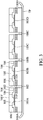
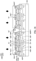
- Figs. 1-7 are cross-sectional views illustrating various steps in the process of manufacturing a semiconductor package structure 800A (as shown in Fig. 8 ), according to some embodiments of the present disclosure.
- a wafer 101 with various devices (not shown) fabricated thereon is provided.
- the various devices (or components) on the wafer 101 are electrically connected to each other by an interconnection layer 102 to form functional circuit.
- the interconnection layer 102 is embedded in inter-metal dielectric (IMD) layers (not shown) and disposed closely adjacent to a top surface 101T of the wafer 101.
- IMD inter-metal dielectric
- a plurality of conductive pads 103 and a passivation layer 104 are sequentially formed on the front side 101T of the wafer 101, wherein each of the conductive pads 103 is partially exposed from the passivation layer 104.
- the wafer 101 may include integrated circuits, such as logic integrated circuits, analog integrated circuits, mixed signal integrated circuits, power integrated circuits, or memory circuits; micro-electro mechanical systems (MEMS); opto-electronic devices; sensors, such as light sensors or fingerprint sensor; or the like.
- the wafer 101 includes an active element (not shown) formed therein, such as a transistor, a metal oxide semiconductor field effect transistor (MOSFET), a metal insulator semiconductor FET (MISFET), a junction field effect transistor (JFET), an insulated gate bipolar transistor (IGBT), a combination thereof, or the like.
- MOSFET metal oxide semiconductor field effect transistor
- MISFET metal insulator semiconductor FET
- JFET junction field effect transistor
- IGBT insulated gate bipolar transistor
- the interconnection layer 102 may include contact plugs formed in an interlayer dielectric (ILD) layer and/or vias and metal lines formed in inter-metal dielectric (IMD) layers (not shown), wherein a portion of the interconnection layer 102 may serve as a seal-ring structure to prevent mechanical damage to the semiconductor dies during the dicing process and prevent the invasion of moisture and chemical contaminants.
- the interconnection layer 102 may be formed by a single damascene process or a dual damascene process.
- a plurality of bumps 105 are correspondingly formed on top surfaces of the plurality of conductive pads 103 exposed from the passivation layer 104, and an insulating layer 106 (e.g. a polyimide layer) is formed to cover the plurality of bumps 105 and the passivation layer 104.
- the passivation layer 104 may include SiO 2 , SiN 3 , SiON, Al 2 O 3 , AlN, polyimide (PI), benzocyclobutene (BCB), polybenzoxazole (PBO), other suitable materials, or a combination thereof.
- the passivation layer 104 may be formed by chemical vapor deposition (CVD), spin-coating, other suitable methods, or a combination thereof.
- the bumps 105 are copper pillars which are used to form an electrical connection between the active elements (not shown) in the wafer 101 and a redistribution layer (e.g. a redistribution layer 620 shown in Fig. 6 ) to be electrically coupled with external circuits.
- a planarization process such as a chemical mechanical polish (CMP) process or other suitable planarization processes, is performed to the insulating layer 106 to expose the top surfaces 105T of the plurality of bumps 105, and a dicing process is performed after the planarization process to divide the wafer 101 into a plurality of individual semiconductor dies (e.g. semiconductor dies 100A/100B/100C/100D).
- the semiconductor dies 100A/100B/100C/100D are disposed with intervals on a dicing tape TP with the interconnection layer 102 exposed from the die edges.
- a metal layer 310 in the interconnection layer 102 of the semiconductor die 100A and a metal layer 320 in the interconnection layer 102 of the semiconductor die 100B are exposed to the gap between the semiconductor die 100A and the semiconductor die 100B.
- the metal layer 310 and the metal layer 320 may serve as a seal-ring structure to prevent mechanical damage to the semiconductor dies during the dicing process.
- the metal layers 310 and 320 may include Cu, W, Ag, Sn, Ni, Co, Cr, Ti, Pb, Au, Bi, Sb, Zn, Zr, Mg, In, Te, Ga, other suitable metal materials, an alloy thereof, or a combination thereof.
- metal layers may be deposited by a process such as a physical vapor deposition (PVD) process, plating, an atomic layer deposition (ALD) process, other suitable processes, or a combination thereof.
- PVD physical vapor deposition
- ALD atomic layer deposition
- the plurality of semiconductor dies (e.g. semiconductor dies 100A/100B/100C/100D) with the conductive pads 103, the passivation layer 104, the bumps 105, and the insulating layer 106 formed on front sides of the semiconductor dies are picked from the dicing tape TP and placed on a carrier substrate 400.
- the front sides of the semiconductor dies may be a front side 100AT of the semiconductor die 100A, a front side 100BT of the semiconductor die 100B, and so on.
- back sides of the semiconductor dies such as the back side 100AB of the semiconductor die 100A and the back side 100BB of the semiconductor die 100B, are attached to a top surface of the carrier substrate 400.
- the semiconductor die 100A and the semiconductor die 100B which will be combined into the semiconductor package structure 800A later are disposed on the carrier substrate 400 with a first gap G1 therebetween
- the semiconductor die 100C and the semiconductor die 100D which will be combined into the semiconductor package structure 800B later are also disposed on the carrier substrate 400 with a first gap G1 therebetween
- the semiconductor die 100B and the semiconductor die 100C, which will not be combined into the same package structure are disposed with a second gap G2 therebetween greater than the first gap G1.
- the second gap G2 may be regarded as "an inter-package gap".
- the width of the first gap G1 may be in a range from about 10 micrometers to about 1000 micrometer
- the width of the second gap G2 may be in a range from about 10 micrometers to about 1000 micrometer, wherein a subsequent dicing process (as shown in Fig. 8 ) may be performed through the second gap G2.
- the difference between the width of the first gap G1 and the width of the second gap G2 may be in a range from about 10 micrometers to about 1000 micrometer.
- the semiconductor die 100A includes a first edge 501 and a second edge 502 opposite the first edge 501, wherein the metal layer 310 is exposed from the second edge 502 to the first gap G1 between the semiconductor die 100A and the semiconductor die 100B.
- the semiconductor die 100B includes a third edge 503 neighboring the second edge 502 of the semiconductor die 100A and a fourth edge 504 opposite the third edge 503, wherein the metal layer 320 is exposed from the third edge 503 to the first gap G1 between the semiconductor die 100A and the semiconductor die 100B.
- the conductive pad 103A and the metal layer 310 are disposed on opposite sides of the front side 100AT of the semiconductor die 100A, and the conductive pad 103B and the metal layer 320 are disposed on opposite sides of the front side 100BT of the semiconductor die 100B.
- an inter-die connector 500 is formed between the metal layer 310 of the semiconductor die 100A and the metal layer 320 of the semiconductor die 100B to provide their electrical connection.
- the inter-die connector 500 includes a first surface 500a adjacent to the front side 100AT of the semiconductor die 100A and the front side 100BT of the semiconductor die 100B and a second surface 500b away from the front side 100AT of the semiconductor die 100A and front side 100BT of the semiconductor die 100B.
- the material of the inter-die connector 500 may include metal (e.g. tungsten, aluminum, or copper), metal alloy, other suitable conductive materials, or a combination thereof.
- the conductive materials may be deposited in the first gap G1 by a process such as a physical vapor deposition (PVD) process, electroplating, electroless plating, metal organic chemical-vapor deposition (MOCVD), an atomic layer deposition (ALD) process, other suitable processes, or a combination thereof.
- PVD physical vapor deposition
- MOCVD metal organic chemical-vapor deposition
- ALD atomic layer deposition
- the inter-die connector 500 is made of copper and is formed by a plating process.
- the plating process for forming the inter-die connector 500 may include a sputtering process to blanketly form a metallic seed layer (not shown) on the carrier substrate 400, a photolithography process to form a patterned photoresist (not shown) with an opening corresponding to the first gap G1, an electro-plating process by connecting the previously formed seed layer to an electrode (not shown) to plate copper in the first gap G1 through the opening of the patterned photoresist, and removing the patterned photoresist and the seed layer which is covered by the patterned photoresist.
- the inter-die connector 500 may be formed by applying metal paste in the first gap G1 to form the electrical connection between the metal layers 310 and 320.
- the material of the metal paste may include metal (e.g. tungsten, aluminum, or copper), metal alloy, other suitable conductive materials, or a combination thereof.
- the aspect ratio of the inter-die connector 500 may be in a range from about 10 micrometers to about 1000 micrometers, for example, about 200 micrometers.
- the inter-die connector 500 partially fills the first gap G1, wherein the first surface 500a of the inter-die connector 500 is substantially level with a top surface 310T of the metal layer 310 and a top surface 320T of the metal layer 320, and the second surface 500b of the inter-die connector 500 is lower than a bottom surface 310B of the metal layer 310 and a bottom surface 320B of the metal layer 320.
- the second surface 500b of the inter-die connector 500 may be coplanar with the back side 100AB of the semiconductor die 100A and the back side 100BB of the semiconductor die 100B.
- the second surface 500b of the inter-die connector 500 abuts the top surface of the carrier substrate 400 that supports the semiconductor dies (e.g. semiconductor dies 100A/100B/100C/100D).
- a molding compound layer 610 is formed to encapsulate the semiconductor dies (e.g. the semiconductor dies 100A/100B/100C/100D) after the formation of the inter-die connector 500.
- the molding compound layer 610 fills the first gap G1 not filled by the inter-die connector 500 and fills the second gap G2 (inter-package gap) between the semiconductor die 100B and the semiconductor die 100C.
- the first surface 500a of the inter-die connector 500 is in contact with the molding compound layer 610.
- a redistribution layer 620 is formed on the molding compound layer 610 and electrically connected to the semiconductor die 100A and the semiconductor die 100B respectively by the plurality of bumps 105 (e.g. the copper pillars) (which are disposed on the front side 100AT of the semiconductor die 100A and the front side 100BT of the semiconductor die 100B).
- a portion of the molding compound layer 610 is disposed between the redistribution layer 620 and the first surface 500a of the inter-die connector 500.
- the molding compound layer 610 may be formed of a resin, a moldable polymer, or the like.
- the molding compound layer 610 may be a resin (e.g. an epoxy resin) which is applied while substantially liquid and then may be cured to transform in the solid.
- the molding compound layer 610 may be an ultraviolet (UV) or thermally cured polymer applied as a gel or malleable solid capable of being disposed around the semiconductor dies (e.g. the semiconductor dies 100A/100B/100C/100D), and then may be cured through a UV or thermal curing process.
- the molding compound layer 610 may be cured with a mold (not shown).
- the redistribution layer 620 includes one or more conductive traces 622 disposed in an inter-metal dielectric (IMD) layer 621.
- IMD inter-metal dielectric
- the inter-metal dielectric layer 621 may be a single layer or a multi-layer structure.
- the inter-metal dielectric layer 621 may be formed of organic materials, which include a polymer base material, non-organic materials, which include silicon nitride (SiNx), silicon oxide (SiOx), graphene, or the like.
- the inter-metal dielectric layer 621 is a low-k dielectric layer (k is the dielectric constant of the dielectric layer). In other embodiments, the inter-metal dielectric layer 621 may be formed of a photo sensitive material, which includes a dry film photoresist, or a taping film.
- the conductive traces 622 may include aluminum, copper, gold, platinum, nickel, tin, a combination thereof, a conductive polymer material, a conductive ceramic material (such as indium tin oxide or indium zinc oxide), or another suitable conductive material.
- the conductive traces 622 may be formed by a deposition process, such as a physical vapor deposition (PVD) process, electroplating, electroless plating, metal organic chemical-vapor deposition (MOCVD), an atomic layer deposition (ALD) process, other suitable processes, or a combination thereof.
- PVD physical vapor deposition
- MOCVD metal organic chemical-vapor deposition
- ALD atomic layer deposition
- a plurality of conductive structures 700 are formed on the redistribution layer 620 by a ball placement process, a screen printing process, an electroplating process, or other suitable processes, and followed by a reflow process.
- the conductive structures 700 may be solder balls, conductive bumps, conductive pillars, or other suitable conductive structures.
- the conductive structures 700 are solder balls, wherein each of the solder balls includes a first conductive material 701 and a second conductive material 702 formed on the first conductive material 701. The material of the first conductive material 701 is different from the material of the second conductive material 702.
- the materials of the first conductive material 701 and the second conductive material 702 may be selected from tin, lead, copper, gold, nickel, a combination thereof, or another suitable conductive material. More specifically, in some embodiments, the first conductive material 701 is copper and covered by the second conductive material 702 which is tin to be advantageous to a subsequent soldering process.
- the carrier substrate 400 is removed and a dicing process is performed with a dicing saw tape (not shown) to form individual semiconductor package structures 800A/800B by cutting through the redistribution layer 620 and a portion of the molding compound layer 610 which fills the second gap G2.
- the semiconductor package structure 800A includes the semiconductor die 100A and the semiconductor die 100B
- the semiconductor package structure 800B includes the semiconductor die 100C and the semiconductor die 100D.
- the semiconductor die 100A and the semiconductor die 100B may have the same functionalities. In other embodiments, the semiconductor die 100A and the semiconductor die 100B may have different functionalities.
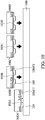
- Fig. 23 is a perspective view illustrating the semiconductor package structure 800A, according to some embodiments of the present disclosure. It should be noted that Fig. 23 does not illustrate all of the elements of the semiconductor package structure 800A for the purpose of simplicity and clarity. In such embodiments, the semiconductor die 100A and the semiconductor die 100B which is in the electrical connection with the semiconductor die 100A by the inter-die connector 500 included in the semiconductor package structure 800A are homogeneous dies which may have the same functionalities.
- Fig. 24 is a perspective view illustrating the semiconductor package structure 800A, according to other embodiments of the present disclosure. It should be noted that Fig. 24 also does not illustrate all of the elements of the semiconductor package structure 800A for the purpose of simplicity and clarity. In such embodiments, the semiconductor die 100A and the semiconductor dies 100B which are in the electrical connection with each other included in the semiconductor package structure 800A are heterogeneous dies which may have different functionalities. As shown in Fig. 24 , the four edges of the semiconductor die 100A are surrounded by the inter-die connector 500 to form electrical connections with the semiconductor dies 100B disposed adjacent to the four edges of the semiconductor die 100A.
- the four semiconductor dies 100B disposed around the semiconductor die 100A may have or may not have the same functionality. It should be noted that the arrangement of the semiconductor dies and the inter-die connector disposed therebetween may vary depending on the product design, and the embodiments of the present disclosure are not limited thereto.
- the grounding lines of the two adjacent dies can be electrically connected directly through the inter-die connector without through additional redistribution layers, such that the conductive path between the two adjacent dies can be effectively reduced, thereby reducing the crosstalk and parasitic inductance between the additional redistribution layers in the semiconductor package structure with high integration density.
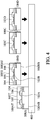
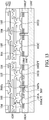
- Figs. 9-15 are cross-sectional views illustrating various steps in the process of manufacturing a semiconductor package structure 800A' according to other embodiments of the present disclosure.
- the embodiments provided in Figs. 9-15 are with respect to a semiconductor package type which is different from the semiconductor package type provided in the embodiments in Figs. 1-8 .
- the semiconductor package type provided in Figs. 1-8 includes a redistribution layer electrically coupled to conductive pads of semiconductor dies through copper pillars
- the semiconductor package type provided in Figs. 9-15 includes a redistribution layer directly electrically coupled to conductive pads of semiconductor dies without through copper pillars. Referring to Fig.
- the structure illustrated in Fig. 9 may be formed sequentially after the step illustrated in Fig. 1 .
- the structure illustrated in Fig. 9 is similar to the structure illustrated in Fig. 3 , except that none of the plurality of bumps 105 and the insulating layer 106 is formed on the plurality of conductive pads 103 and the passivation layer 104 in the structure illustrated in Fig. 9 . Thus, the details are not repeated for brevity.
- the plurality of semiconductor dies e.g. semiconductor dies 100A'/100B'/100C'/100D'
- the conductive pads 103 e.g. the conductive pads 103A/103B/103C/103D
- the passivation layer 104 formed on front sides of the semiconductor dies are picked from the dicing tape TP and flipped upside down to place on a carrier substrate 400.
- the front sides of the semiconductor dies may be a front side 100A'T of the semiconductor die 100A', a front side 100B'T of the semiconductor die 100B', and so on.
- the passivation layer 104 formed on the front sides of the semiconductor dies are attached to a top surface of the carrier substrate 400.
- the semiconductor die 100A' and the semiconductor die 100B' which will be combined into the semiconductor package structure 800A' later are disposed on the carrier substrate 400 with a first gap G1 therebetween
- the semiconductor die 100C' and the semiconductor die 100D' which will be combined into the semiconductor package structure 800B' later are also disposed on the carrier substrate 400 with a first gap G1 therebetween
- a subsequent dicing process (as shown in Fig. 15 ) may be performed through the second gap G2.
- the semiconductor die 100A' includes a first edge 501' and a second edge 502' opposite the first edge 501', wherein the metal layer 310' in the interconnection layer 102' is exposed from the second edge 502' to the first gap G1 between the semiconductor die 100A' and the semiconductor die 100B'.
- the semiconductor die 100B' includes a third edge 503' neighboring the second edge 502' of the semiconductor die 100A' and a fourth edge 504' opposite the third edge 503', wherein the metal layer 320' in the interconnection layer 102' is exposed from the third edge 503' to the first gap G1 between the semiconductor die 100A' and the semiconductor die 100B'.
- the conductive pad 103A and the metal layer 310' are disposed on opposite sides of the front side 100A'T of the semiconductor die 100A', and the conductive pad 103B and the metal layer 320' are disposed on opposite sides of the front side 100B'T of the semiconductor die 100B'.
- the metal layer 310' and the metal layer 320' may serve as a seal-ring structure to prevent mechanical damage to the semiconductor dies during the dicing process and prevent the invasion of moisture and chemical contaminants.
- an inter-die connector 500' is formed between the metal layer 310' of the semiconductor die 100A' and the metal layer 320' of the semiconductor die 100B' to form the electrical connection, wherein the inter-die connector 500' includes a first surface 500'a adjacent to the front side 100A'T of the semiconductor die 100A' and the front side 100B'T of the semiconductor die 100B' and a second surface 500'b away from the front side 100A'T of the semiconductor die 100A', the front side 100B'T of the semiconductor die 100B', and the top surface of the carrier substrate 400.
- the inter-die connector 500' partially fills the first gap G1 between the semiconductor die 100A' and the semiconductor die 100B'.
- the first surface 500'a of the inter-die connector 500' protrudes beyond the front side 100A'T of the semiconductor die 100A' and the front side 100B'T of the semiconductor die 100B'.
- the material and method for forming the inter-die connector 500' may be selected from those of the above-mentioned inter-die connector 500. The details are not repeated for brevity.
- a molding compound layer 610' is formed to encapsulate the semiconductor dies (e.g. the semiconductor dies 100A'/100B'/100C'/100D') after the formation of the inter-die connector 500', wherein the second surface 500'b of the inter-die connector 500' is in contact with the molding compound layer 610'.
- the molding compound layer 610' encapsulates the sidewall surfaces and the back side 100A'B of the semiconductor die 100A' and the sidewall surface and the back side 100B'B of the semiconductor die 100B'.
- the molding compound layer 610' fills the first gap G1 not filled by the inter-die connector 500' and is in contact with the second surface 500'b of the inter-die connector 500'.
- the redistribution layer 620' is respectively electrically coupled to the semiconductor dies (e.g. the semiconductor dies 100A'/100B'/100C'/100D') through the plurality of conductive pads 103 (e.g. the conductive pads 103A/103B/103C/103D) formed on the front sides of the semiconductor dies.
- the material and method for forming the molding compound layer 610' and the redistribution layer 620' respectively may be selected from those of the above-mentioned molding compound layer 610 and redistribution layer 620. The details are not repeated for brevity.
- a plurality of conductive structures 700 are formed on the redistribution layer 620' by a ball placement process, a screen printing process, an electroplating process, or other suitable processes, and followed by a reflow process.
- the conductive structures 700 may be solder balls, conductive bumps, conductive pillars, or other suitable conductive structures. It should be noted that the material of the plurality of conductive structures 700 may be selected from that of the above-mentioned conductive structures 700. The details are not repeated for brevity.
- a dicing process is performed to form individual semiconductor package structures 800A'/800B' by cutting through the redistribution layer 620' and a portion of the molding compound layer 610' which fills the second gap G2.
- the semiconductor package structure 800A' includes the semiconductor die 100A' and the semiconductor die 100B'
- the semiconductor package structure 800B' includes the semiconductor die 100C' and the semiconductor die 100D'.
- the semiconductor die 100A' and the semiconductor die 100B' may have the same functionalities (as discussed with respect to Fig. 25). In other embodiments, the semiconductor die 100A' and the semiconductor die 100B' may have different functionalities (as discussed with respect to Fig. 26).
- the arrangement of the inter-die connector is also applicable to the embodiments provided in Figs. 9-15 of the present disclosure.
- the grounding lines of the two adjacent dies can be electrically connected directly through the inter-die connector without through additional redistribution layers, such that the conductive path between the two adjacent dies can be effectively reduced, thereby reducing the crosstalk and parasitic inductance between the additional redistribution layers in the semiconductor package structure with high integration density.
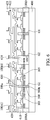
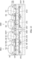
- Figs. 16-22 are cross-sectional views illustrating various steps in the process of manufacturing a semiconductor package structure 800A" according to other embodiments of the present disclosure.
- the embodiments provided in Figs. 16-22 are with respect to a semiconductor package type which is different from the semiconductor package type provided in the embodiments in Figs. 1-8 and the semiconductor package type provided in the embodiments in Figs. 9-15 .
- the semiconductor package type provided in Figs. 1-8 includes a redistribution layer electrically coupled to conductive pads of semiconductor dies through copper pillars
- the semiconductor package type provided in Figs. 9-15 includes a redistribution layer directly electrically coupled to conductive pads of semiconductor dies
- the semiconductor package type provided in Figs. 16-22 includes a redistribution layer electrically coupled to conductive pads of semiconductor dies through micro-bumps.
- the structure may be formed sequentially after the step illustrated in Fig. 1 .
- a plurality of bumps 1800 are respectively formed on top surfaces of the plurality of conductive pads 103 exposed from the passivation layer 104.
- the bumps 1800 are micro-bumps which are used to form an electrical connection between the active elements in the wafer 101 and a redistribution layer (e.g. a redistribution layer 620" shown in Fig. 18 ) to be electrically coupled with external circuits.
- each of the bumps 1800 includes a first conductive material 1801 and a second conductive material 1802 formed on the first conductive material 1801.
- the material of the first conductive material 1801 is different from the material of the second conductive material 1802.
- the materials of the first conductive material 1801 and the second conductive material 1802 may be selected from tin, lead, copper, gold, nickel, a combination thereof, or another suitable conductive material.
- a dicing process is performed to divide the wafer 101 into a plurality of semiconductor dies (e.g. semiconductor dies 100A"/100B"/100C"/100D").
- the semiconductor dies 100A"/100B"/100C"/100D" are disposed with intervals on a dicing tape TP, wherein a metal layer 310" in the interconnection layer 102" of the semiconductor die 100A” and a metal layer 320" in the interconnection layer 102" of the semiconductor die 100B" are exposed to the gap between the semiconductor die 100A" and the semiconductor die 100B".
- the plurality of semiconductor dies (e.g. semiconductor dies 100A"/100B"/100C"/100D") with the conductive pads 103 (e.g. conductive pads 103A/103B/103C/103D), the passivation layer 104, and bumps 1800 formed on front sides of the semiconductor dies are picked from the dicing tape TP and flipped upside down to place on a redistribution layer 620" provided on a carrier substrate 400.
- the front sides of the semiconductor dies may be a front side 100A"T of the semiconductor die 100A", a front side 100B"T of the semiconductor die 100B", and so on.
- the plurality of first bumps 1800 on the front sides of the semiconductor dies are bonded to the redistribution layer 620" on the carrier substrate 400.
- the semiconductor die 100A" and the semiconductor die 100B" which will be combined into the semiconductor package structure 800A” later are disposed on the carrier substrate 400 with a first gap G1 therebetween
- the semiconductor die 100C" and the semiconductor die 100D" which will be combined into the semiconductor package structure 800B” later are also disposed on the carrier substrate 400 with a first gap G1 therebetween
- a subsequent dicing process (as shown in Fig. 22 ) may be performed through the second gap G2.
- the semiconductor die 100A" includes a first edge 501" and a second edge 502" opposite the first edge 501", wherein the metal layer 310" in the interconnection layer 102" is exposed from the second edge 502" to the first gap G1 between the semiconductor die 100A” and the semiconductor die 100B".
- the semiconductor die 100B" includes a third edge 503" neighboring the second edge 502" of the semiconductor die 100A” and a fourth edge 504" opposite the third edge 503", wherein the metal layer 320" in the interconnection layer 102" is exposed from the third edge 503" to the first gap G1 between the semiconductor die 100A" and the semiconductor die 100B".
- the conductive pad 103A and the metal layer 310" are disposed on opposite sides of the front side 100A"T of the semiconductor die 100A", and the conductive pad 103B and the metal layer 320" are disposed on opposite sides of the front side 100B"T of the semiconductor die 100B".
- the metal layer 310" and the metal layer 320" may serve as a seal-ring structure to prevent mechanical damage to the semiconductor dies during the dicing process and prevent the invasion of moisture and chemical contaminants.
- an underfill material 2000 is formed to surround the plurality of bumps 1800.
- the underfill material 2000 is made of or includes a polymer material.
- the underfill material 2000 may include an epoxy-based resin.
- the formation of the underfill material 2000 includes a dispensing process, an application process, other applicable processes, or a combination thereof.
- a thermal curing process is used during the formation of the underfill material 2000.
- an inter-die connector 500" is formed between the metal layer 310"of the semiconductor die 100A" and the metal layer 320" of the semiconductor die 100B" to form the electrical connection, wherein the inter-die connector 500" includes a first surface 500"a adjacent to the front side 100A"T of the semiconductor die 100A” and the front side 100B"T of the semiconductor die 100B” and a second surface 500"b away from the front side 100A"T of the semiconductor die 100A" and front side 100B"T of the semiconductor die 100B".
- the inter-die connector 500" is formed on the underfill material 2000, wherein the first surface 500"a of the inter-die connector 500" is in contact with the underfill material 2000.
- the material and method for forming the inter-die connector 500" may be selected from those of the above-mentioned inter-die connector 500. The details are not repeated for brevity.
- a molding compound layer 610" is formed to encapsulate the semiconductor dies (e.g. the semiconductor dies 100A"/100B"/100C”/100D") after the formation of the inter-die connector 500", wherein the second surface 500"b of the inter-die connector 500" is in contact with the molding compound layer 610".
- the molding compound layer 610" encapsulates the sidewall surfaces and the back side 100A"B of the semiconductor die 100A", the sidewall surface and the back side 100B"B of the semiconductor die 100B", and the underfill material 2000, wherein the molding compound layer 610" fills the first gap G1 not filled by the inter-die connector 500" and is in contact with the second surface 500"b of the inter-die connector 500".
- the structure illustrated in Fig. 20 is flipped upside down, and the carrier substrate 400 is removed to form a plurality of conductive structures 700 over the front sides of the semiconductor dies and in contact with the redistribution layer 620" which is respectively electrically coupled to the semiconductor dies (e.g. the semiconductor dies 100A"/100B"/100C"/100D") through the plurality of conductive bumps 1800 formed on the front sides of the semiconductor dies.
- the material and method for forming the conductive structures 700 may be selected from those of the conductive structures 700 with respect to Fig. 7 . The details are not repeated for brevity.
- a dicing process is performed to form individual semiconductor package structures 800A"/800B" by cutting through the redistribution layer 620" and a portion of the molding compound layer 610" which fills the second gap G2.
- the semiconductor package structure 800A" includes the semiconductor die 100A" and the semiconductor die 100B
- the semiconductor package structure 800B" includes the semiconductor die 100C" and the semiconductor die 100D".
- the semiconductor die 100A" and the semiconductor die 100B" may have the same functionalities (as discussed with respect to Fig. 25). In other embodiments, the semiconductor die 100A" and the semiconductor die 100B" may have different functionalities (as discussed with respect to Fig. 26).
- the arrangement of the inter-die connector is also applicable to the embodiments provided in Figs. 16-22 of the present disclosure.
- the grounding lines of the two adjacent dies can be electrically connected directly through the inter-die connector without through additional redistribution layers, such that the conductive path between the two adjacent dies can be effectively reduced, thereby reducing the crosstalk and parasitic inductance between the additional redistribution layers in the semiconductor package structure with high integration density.
Landscapes
- Structures Or Materials For Encapsulating Or Coating Semiconductor Devices Or Solid State Devices (AREA)
- Engineering & Computer Science (AREA)
- Manufacturing & Machinery (AREA)
Abstract
Description
- This application claims the benefit of
U.S. Provisional Application No. 62/770,861 filed on November 23, 2018 - The disclosure relates to a semiconductor package, and more particularly to a semiconductor package that includes an inter-die connector.
- The semiconductor packaging process is an important step in the fabrication of electronic products. Semiconductor packages not only protect the semiconductor dies therein from outer environmental contaminants but also provide electrical connection paths between the electronic components inside and those outside of the semiconductor packages. For example, a semiconductor package contains wires that may be used to form conductive paths.
- The semiconductor industry continues to improve the integration density of various electronic components (e.g. transistors, diodes, resistors, capacitors, and so on.) by continual reductions in minimum feature size, which allow more components to be integrated into a given area. These smaller electronic components also use a smaller package that utilizes less area or a smaller height, in some applications. When the semiconductor packages become denser, the crosstalk generated between conductive paths increases correspondingly.
- While existing semiconductor package structures have been generally adequate for their intended purposes, they have not been satisfactory in all respects. There is a particular need for further improvements in the reduction of the crosstalk between electronic components.
- In one embodiment of the present disclosure, a semiconductor package structure is provided, wherein the semiconductor package structure includes a first semiconductor die and a second semiconductor die neighboring the first semiconductor die. The first semiconductor die includes a first edge, a second edge opposite the first edge, and a first metal layer exposed from the second edge. The second semiconductor includes a third edge neighboring the second edge of the first semiconductor die, a fourth edge opposite the third edge, and a second metal layer exposed from the third edge. The first metal layer of the first semiconductor die is electrically connected to the second metal layer of the second semiconductor die.
- In one embodiment of the present disclosure, a method for forming a semiconductor package structure is provided, wherein the method for forming a semiconductor package structure includes providing a first semiconductor die on a carrier substrate, wherein the first semiconductor die includes a first edge, a second edge opposite the first edge, and a first metal layer exposed from the second edge, wherein the first metal layer is disposed in an interconnection layer of the first semiconductor die; and providing a second semiconductor die neighboring the first semiconductor die on the carrier substrate, wherein the second semiconductor die includes a third edge neighboring the second edge of the first semiconductor die, a fourth edge opposite the third edge, and a second metal layer exposed from the third edge, wherein the second metal layer is disposed in an interconnection layer of the second semiconductor die; and forming an electrical connection between the first metal layer of the first semiconductor die and the second metal layer of the second semiconductor die.
- A detailed description is given in the following embodiments with reference to the accompanying drawings.
- Aspects of this disclosure are best understood from the following detailed description when read with the accompanying figures. It should be noted that, in accordance with common practice in the industry, various features are not drawn to scale. In fact, the dimensions of the various features may be arbitrarily increased or reduced for clarity of discussion.
-
Figs. 1-8 are cross-sectional views illustrating various steps in the process of manufacturing a semiconductor package structure, according to some embodiments of the present disclosure. -
Figs. 9-15 are cross-sectional views illustrating various steps in the process of manufacturing a semiconductor package structure, according to other embodiments of the present disclosure. -
Figs. 16-22 are cross-sectional views illustrating various steps in the process of manufacturing a semiconductor package structure, according to other embodiments of the present disclosure. -
Fig. 23 is a perspective view illustrating an exemplary semiconductor package structure, according to some embodiments of the present disclosure. -
Fig. 24 is a perspective view illustrating an exemplary semiconductor package structure, according to other embodiments of the present disclosure. - The following disclosure provides many different embodiments, or examples, for implementing different features of the subject matter provided. These are, of course, merely examples and are not intended to be limiting. For example, the formation of a first feature over or on a second feature in the description that follows may include embodiments in which the first and second features are formed in direct contact, and may also include embodiments in which additional features may be formed between the first and second features. In addition, the present disclosure may repeat reference numerals and/or letters in the various examples. This repetition is for the purpose of simplicity and clarity and does not in itself dictate a relationship between the various embodiments and/or configurations discussed.
- Furthermore, spatially relative terms, such as "over", "below," "lower," and the like, may be used herein for ease of description to describe one element or feature's relationship to another element(s) or feature(s) as illustrated in the figures. The spatially relative terms are intended to encompass different orientations of the device in use or operation in addition to the orientation depicted in the figures. The apparatus may be otherwise oriented and the spatially relative descriptors used herein may likewise be interpreted accordingly.
- The terms "about", "approximately", and "substantially" used herein generally refer to the value of an error or a range within 20 percent, preferably within 10 percent, and more preferably within 5 percent, within 3 percent, within 2 percent, within 1 percent, or within 0.5 percent. If there is no specific description, the values mentioned are to be regarded as an approximation that is an error or range expressed as "about", "approximate", or "substantially".
- Although some embodiments are discussed with operations performed in a particular order, these operations may be performed in another logical order. Additional features can be provided to the semiconductor structures in embodiments of the present disclosure. Some of the features described below can be replaced or eliminated for different embodiments.
- Embodiments of the present disclosure provide a semiconductor package structure which includes an inter-die connector to form an electrical connection between two adjacent dies. The inter-die connector is disposed between two adjacent dies to make an electrical connection between the metal layers respectively exposed from edges of the two adjacent die. By setting the inter-die connector, the grounding lines of the two adjacent dies can be electrically connected directly through the inter-die connector without through additional redistribution layers, such that the conductive path between the two adjacent dies can be effectively reduced, thereby reducing the crosstalk and parasitic inductance between the additional redistribution layers in the semiconductor package structure with high integration density.
-
Figs. 1-7 are cross-sectional views illustrating various steps in the process of manufacturing asemiconductor package structure 800A (as shown inFig. 8 ), according to some embodiments of the present disclosure. Referring toFig. 1 , awafer 101 with various devices (not shown) fabricated thereon is provided. The various devices (or components) on thewafer 101 are electrically connected to each other by aninterconnection layer 102 to form functional circuit. As shown inFig. 1 , theinterconnection layer 102 is embedded in inter-metal dielectric (IMD) layers (not shown) and disposed closely adjacent to atop surface 101T of thewafer 101. A plurality ofconductive pads 103 and apassivation layer 104 are sequentially formed on thefront side 101T of thewafer 101, wherein each of theconductive pads 103 is partially exposed from thepassivation layer 104. - In some embodiments, the
wafer 101 may include integrated circuits, such as logic integrated circuits, analog integrated circuits, mixed signal integrated circuits, power integrated circuits, or memory circuits; micro-electro mechanical systems (MEMS); opto-electronic devices; sensors, such as light sensors or fingerprint sensor; or the like. In some embodiments, thewafer 101 includes an active element (not shown) formed therein, such as a transistor, a metal oxide semiconductor field effect transistor (MOSFET), a metal insulator semiconductor FET (MISFET), a junction field effect transistor (JFET), an insulated gate bipolar transistor (IGBT), a combination thereof, or the like. It should be noted thatFig. 1 does not illustrate the components of thewafer 101 under theinterconnection layer 102 for the purpose of simplicity and clarity. - In some embodiments, the
interconnection layer 102 may include contact plugs formed in an interlayer dielectric (ILD) layer and/or vias and metal lines formed in inter-metal dielectric (IMD) layers (not shown), wherein a portion of theinterconnection layer 102 may serve as a seal-ring structure to prevent mechanical damage to the semiconductor dies during the dicing process and prevent the invasion of moisture and chemical contaminants. For example, theinterconnection layer 102 may be formed by a single damascene process or a dual damascene process. - Referring to
Fig. 2 , in some embodiments, a plurality ofbumps 105 are correspondingly formed on top surfaces of the plurality ofconductive pads 103 exposed from thepassivation layer 104, and an insulating layer 106 (e.g. a polyimide layer) is formed to cover the plurality ofbumps 105 and thepassivation layer 104. In some embodiments, thepassivation layer 104 may include SiO2, SiN3, SiON, Al2O3, AlN, polyimide (PI), benzocyclobutene (BCB), polybenzoxazole (PBO), other suitable materials, or a combination thereof. In some embodiments, thepassivation layer 104 may be formed by chemical vapor deposition (CVD), spin-coating, other suitable methods, or a combination thereof. In some embodiments, thebumps 105 are copper pillars which are used to form an electrical connection between the active elements (not shown) in thewafer 101 and a redistribution layer (e.g. aredistribution layer 620 shown inFig. 6 ) to be electrically coupled with external circuits. - Referring to
Fig. 3 , a planarization process, such as a chemical mechanical polish (CMP) process or other suitable planarization processes, is performed to theinsulating layer 106 to expose thetop surfaces 105T of the plurality ofbumps 105, and a dicing process is performed after the planarization process to divide thewafer 101 into a plurality of individual semiconductor dies (e.g. semiconductor dies 100A/100B/100C/100D). As shown inFig. 3 , after the dicing process, the semiconductor dies 100A/100B/100C/100D are disposed with intervals on a dicing tape TP with theinterconnection layer 102 exposed from the die edges. More specifically, ametal layer 310 in theinterconnection layer 102 of thesemiconductor die 100A and ametal layer 320 in theinterconnection layer 102 of thesemiconductor die 100B are exposed to the gap between thesemiconductor die 100A and thesemiconductor die 100B. In some embodiments, themetal layer 310 and themetal layer 320 may serve as a seal-ring structure to prevent mechanical damage to the semiconductor dies during the dicing process. - In some embodiments, the
metal layers - Subsequently, referring to
Fig. 4 , the plurality of semiconductor dies (e.g. semiconductor dies 100A/100B/ 100C/100D) with theconductive pads 103, thepassivation layer 104, thebumps 105, and the insulatinglayer 106 formed on front sides of the semiconductor dies are picked from the dicing tape TP and placed on acarrier substrate 400. For example, the front sides of the semiconductor dies may be a front side 100AT of the semiconductor die 100A, a front side 100BT of the semiconductor die 100B, and so on. Specifically, back sides of the semiconductor dies, such as the back side 100AB of the semiconductor die 100A and the back side 100BB of the semiconductor die 100B, are attached to a top surface of thecarrier substrate 400. - Referring to
Fig. 5 , in some embodiments, the semiconductor die 100A and the semiconductor die 100B which will be combined into thesemiconductor package structure 800A later (as shown inFig. 8 ) are disposed on thecarrier substrate 400 with a first gap G1 therebetween, the semiconductor die 100C and thesemiconductor die 100D which will be combined into thesemiconductor package structure 800B later (as shown inFig. 8 ) are also disposed on thecarrier substrate 400 with a first gap G1 therebetween. Meanwhile, the semiconductor die 100B and the semiconductor die 100C, which will not be combined into the same package structure, are disposed with a second gap G2 therebetween greater than the first gap G1. The second gap G2 may be regarded as "an inter-package gap". For example, the width of the first gap G1 may be in a range from about 10 micrometers to about 1000 micrometer, and the width of the second gap G2 may be in a range from about 10 micrometers to about 1000 micrometer, wherein a subsequent dicing process (as shown inFig. 8 ) may be performed through the second gap G2. Furthermore, the difference between the width of the first gap G1 and the width of the second gap G2 may be in a range from about 10 micrometers to about 1000 micrometer. - Still referring to
Fig. 5 , the semiconductor die 100A includes afirst edge 501 and asecond edge 502 opposite thefirst edge 501, wherein themetal layer 310 is exposed from thesecond edge 502 to the first gap G1 between the semiconductor die 100A and the semiconductor die 100B. The semiconductor die 100B includes athird edge 503 neighboring thesecond edge 502 of the semiconductor die 100A and afourth edge 504 opposite thethird edge 503, wherein themetal layer 320 is exposed from thethird edge 503 to the first gap G1 between the semiconductor die 100A and the semiconductor die 100B. In some embodiments, theconductive pad 103A and themetal layer 310 are disposed on opposite sides of the front side 100AT of the semiconductor die 100A, and theconductive pad 103B and themetal layer 320 are disposed on opposite sides of the front side 100BT of the semiconductor die 100B. - According to some embodiments of the present disclosure, as shown in
Fig. 5 , aninter-die connector 500 is formed between themetal layer 310 of the semiconductor die 100A and themetal layer 320 of the semiconductor die 100B to provide their electrical connection. Theinter-die connector 500 includes afirst surface 500a adjacent to the front side 100AT of the semiconductor die 100A and the front side 100BT of the semiconductor die 100B and asecond surface 500b away from the front side 100AT of the semiconductor die 100A and front side 100BT of the semiconductor die 100B. - In some embodiments, the material of the
inter-die connector 500 may include metal (e.g. tungsten, aluminum, or copper), metal alloy, other suitable conductive materials, or a combination thereof. For example, the conductive materials may be deposited in the first gap G1 by a process such as a physical vapor deposition (PVD) process, electroplating, electroless plating, metal organic chemical-vapor deposition (MOCVD), an atomic layer deposition (ALD) process, other suitable processes, or a combination thereof. - Specifically, according to some embodiments of the present disclosure, the
inter-die connector 500 is made of copper and is formed by a plating process. For example, the plating process for forming theinter-die connector 500 may include a sputtering process to blanketly form a metallic seed layer (not shown) on thecarrier substrate 400, a photolithography process to form a patterned photoresist (not shown) with an opening corresponding to the first gap G1, an electro-plating process by connecting the previously formed seed layer to an electrode (not shown) to plate copper in the first gap G1 through the opening of the patterned photoresist, and removing the patterned photoresist and the seed layer which is covered by the patterned photoresist. In other embodiments, theinter-die connector 500 may be formed by applying metal paste in the first gap G1 to form the electrical connection between the metal layers 310 and 320. The material of the metal paste may include metal (e.g. tungsten, aluminum, or copper), metal alloy, other suitable conductive materials, or a combination thereof. For example, as shown in the cross-sectional view illustrating inFig. 5 , the aspect ratio of theinter-die connector 500 may be in a range from about 10 micrometers to about 1000 micrometers, for example, about 200 micrometers. - Still referring to
Fig. 5 , in some embodiments, theinter-die connector 500 partially fills the first gap G1, wherein thefirst surface 500a of theinter-die connector 500 is substantially level with atop surface 310T of themetal layer 310 and a top surface 320T of themetal layer 320, and thesecond surface 500b of theinter-die connector 500 is lower than abottom surface 310B of themetal layer 310 and abottom surface 320B of themetal layer 320. Specifically, thesecond surface 500b of theinter-die connector 500 may be coplanar with the back side 100AB of the semiconductor die 100A and the back side 100BB of the semiconductor die 100B. In other words, thesecond surface 500b of theinter-die connector 500 abuts the top surface of thecarrier substrate 400 that supports the semiconductor dies (e.g. semiconductor dies 100A/100B/ 100C/100D). - Referring to
Fig. 6 , amolding compound layer 610 is formed to encapsulate the semiconductor dies (e.g. the semiconductor dies 100A/100B/ 100C/100D) after the formation of theinter-die connector 500. Themolding compound layer 610 fills the first gap G1 not filled by theinter-die connector 500 and fills the second gap G2 (inter-package gap) between the semiconductor die 100B and the semiconductor die 100C. Thus, thefirst surface 500a of theinter-die connector 500 is in contact with themolding compound layer 610. After the formation of themolding compound layer 610, aredistribution layer 620 is formed on themolding compound layer 610 and electrically connected to the semiconductor die 100A and the semiconductor die 100B respectively by the plurality of bumps 105 (e.g. the copper pillars) (which are disposed on the front side 100AT of the semiconductor die 100A and the front side 100BT of the semiconductor die 100B). A portion of themolding compound layer 610 is disposed between theredistribution layer 620 and thefirst surface 500a of theinter-die connector 500. - For example, the
molding compound layer 610 may be formed of a resin, a moldable polymer, or the like. Themolding compound layer 610 may be a resin (e.g. an epoxy resin) which is applied while substantially liquid and then may be cured to transform in the solid. In other embodiments, themolding compound layer 610 may be an ultraviolet (UV) or thermally cured polymer applied as a gel or malleable solid capable of being disposed around the semiconductor dies (e.g. the semiconductor dies 100A/100B/ 100C/100D), and then may be cured through a UV or thermal curing process. Themolding compound layer 610 may be cured with a mold (not shown). - In some embodiments, the
redistribution layer 620 includes one or moreconductive traces 622 disposed in an inter-metal dielectric (IMD)layer 621. For example, at least one of the conductive traces 622 is electrically coupled to the semiconductor die 100A, and at least one of the conductive traces 622 is electrically coupled to the semiconductor die 100B. For example, the inter-metaldielectric layer 621 may be a single layer or a multi-layer structure. Moreover, the inter-metaldielectric layer 621 may be formed of organic materials, which include a polymer base material, non-organic materials, which include silicon nitride (SiNx), silicon oxide (SiOx), graphene, or the like. In some embodiments, the inter-metaldielectric layer 621 is a low-k dielectric layer (k is the dielectric constant of the dielectric layer). In other embodiments, the inter-metaldielectric layer 621 may be formed of a photo sensitive material, which includes a dry film photoresist, or a taping film. - For example, the conductive traces 622 may include aluminum, copper, gold, platinum, nickel, tin, a combination thereof, a conductive polymer material, a conductive ceramic material (such as indium tin oxide or indium zinc oxide), or another suitable conductive material. In some embodiments, the conductive traces 622 may be formed by a deposition process, such as a physical vapor deposition (PVD) process, electroplating, electroless plating, metal organic chemical-vapor deposition (MOCVD), an atomic layer deposition (ALD) process, other suitable processes, or a combination thereof.
- Referring to
Fig. 7 , a plurality ofconductive structures 700 are formed on theredistribution layer 620 by a ball placement process, a screen printing process, an electroplating process, or other suitable processes, and followed by a reflow process. In some embodiments, theconductive structures 700 may be solder balls, conductive bumps, conductive pillars, or other suitable conductive structures. Specifically, according to some embodiments of the present disclosure, theconductive structures 700 are solder balls, wherein each of the solder balls includes a firstconductive material 701 and a secondconductive material 702 formed on the firstconductive material 701. The material of the firstconductive material 701 is different from the material of the secondconductive material 702. For example, the materials of the firstconductive material 701 and the secondconductive material 702 may be selected from tin, lead, copper, gold, nickel, a combination thereof, or another suitable conductive material. More specifically, in some embodiments, the firstconductive material 701 is copper and covered by the secondconductive material 702 which is tin to be advantageous to a subsequent soldering process. - Referring to
Fig. 8 , thecarrier substrate 400 is removed and a dicing process is performed with a dicing saw tape (not shown) to form individualsemiconductor package structures 800A/800B by cutting through theredistribution layer 620 and a portion of themolding compound layer 610 which fills the second gap G2. As shown inFig. 8 , thesemiconductor package structure 800A includes the semiconductor die 100A and the semiconductor die 100B, and thesemiconductor package structure 800B includes the semiconductor die 100C and thesemiconductor die 100D. According to some embodiments of the present disclosure, the semiconductor die 100A and the semiconductor die 100B may have the same functionalities. In other embodiments, the semiconductor die 100A and the semiconductor die 100B may have different functionalities. - Referring to
Fig. 8 along withFig. 23. Fig. 23 is a perspective view illustrating thesemiconductor package structure 800A, according to some embodiments of the present disclosure. It should be noted thatFig. 23 does not illustrate all of the elements of thesemiconductor package structure 800A for the purpose of simplicity and clarity. In such embodiments, the semiconductor die 100A and thesemiconductor die 100B which is in the electrical connection with the semiconductor die 100A by theinter-die connector 500 included in thesemiconductor package structure 800A are homogeneous dies which may have the same functionalities. - On the other hand, referring to
Fig. 8 along withFig. 24. Fig. 24 is a perspective view illustrating thesemiconductor package structure 800A, according to other embodiments of the present disclosure. It should be noted thatFig. 24 also does not illustrate all of the elements of thesemiconductor package structure 800A for the purpose of simplicity and clarity. In such embodiments, the semiconductor die 100A and the semiconductor dies 100B which are in the electrical connection with each other included in thesemiconductor package structure 800A are heterogeneous dies which may have different functionalities. As shown inFig. 24 , the four edges of the semiconductor die 100A are surrounded by theinter-die connector 500 to form electrical connections with the semiconductor dies 100B disposed adjacent to the four edges of the semiconductor die 100A. Furthermore, the four semiconductor dies 100B disposed around the semiconductor die 100A may have or may not have the same functionality. It should be noted that the arrangement of the semiconductor dies and the inter-die connector disposed therebetween may vary depending on the product design, and the embodiments of the present disclosure are not limited thereto. - As described above, according to the embodiments of the present disclosure, by the arrangement of the inter-die connector to form an electrical connection between two adjacent dies, the grounding lines of the two adjacent dies can be electrically connected directly through the inter-die connector without through additional redistribution layers, such that the conductive path between the two adjacent dies can be effectively reduced, thereby reducing the crosstalk and parasitic inductance between the additional redistribution layers in the semiconductor package structure with high integration density.
-
Figs. 9-15 are cross-sectional views illustrating various steps in the process of manufacturing asemiconductor package structure 800A' according to other embodiments of the present disclosure. Specifically, the embodiments provided inFigs. 9-15 are with respect to a semiconductor package type which is different from the semiconductor package type provided in the embodiments inFigs. 1-8 . According to some embodiments of the present disclosure, the semiconductor package type provided inFigs. 1-8 includes a redistribution layer electrically coupled to conductive pads of semiconductor dies through copper pillars, and the semiconductor package type provided inFigs. 9-15 includes a redistribution layer directly electrically coupled to conductive pads of semiconductor dies without through copper pillars. Referring toFig. 9 , the structure may be formed sequentially after the step illustrated inFig. 1 . According to some embodiments of the present disclosure, the structure illustrated inFig. 9 is similar to the structure illustrated inFig. 3 , except that none of the plurality ofbumps 105 and the insulatinglayer 106 is formed on the plurality ofconductive pads 103 and thepassivation layer 104 in the structure illustrated inFig. 9 . Thus, the details are not repeated for brevity. - Referring to
Fig. 10 , the plurality of semiconductor dies (e.g. semiconductor dies 100A'/100B'/100C'/100D') with the conductive pads 103 (e.g. theconductive pads 103A/103B/ 103C/103D) and thepassivation layer 104 formed on front sides of the semiconductor dies are picked from the dicing tape TP and flipped upside down to place on acarrier substrate 400. For example, the front sides of the semiconductor dies may be afront side 100A'T of the semiconductor die 100A', afront side 100B'T of the semiconductor die 100B', and so on. Specifically, thepassivation layer 104 formed on the front sides of the semiconductor dies are attached to a top surface of thecarrier substrate 400. - Referring to
Fig. 11 , in some embodiments, the semiconductor die 100A' and thesemiconductor die 100B' which will be combined into thesemiconductor package structure 800A' later are disposed on thecarrier substrate 400 with a first gap G1 therebetween, thesemiconductor die 100C' and thesemiconductor die 100D' which will be combined into thesemiconductor package structure 800B' later are also disposed on thecarrier substrate 400 with a first gap G1 therebetween, and there is a second gap G2 larger than first gap G1 remaining between the semiconductor die 100B' and thesemiconductor die 100C'. In some embodiments, a subsequent dicing process (as shown inFig. 15 ) may be performed through the second gap G2. - Still referring to
Fig. 11 , the semiconductor die 100A' includes a first edge 501' and a second edge 502' opposite the first edge 501', wherein the metal layer 310' in the interconnection layer 102' is exposed from the second edge 502' to the first gap G1 between the semiconductor die 100A' and thesemiconductor die 100B'. The semiconductor die 100B' includes a third edge 503' neighboring the second edge 502' of the semiconductor die 100A' and a fourth edge 504' opposite the third edge 503', wherein the metal layer 320' in the interconnection layer 102' is exposed from the third edge 503' to the first gap G1 between the semiconductor die 100A' and thesemiconductor die 100B'. In some embodiments, theconductive pad 103A and the metal layer 310' are disposed on opposite sides of thefront side 100A'T of the semiconductor die 100A', and theconductive pad 103B and the metal layer 320' are disposed on opposite sides of thefront side 100B'T of thesemiconductor die 100B'. In some embodiments, the metal layer 310' and the metal layer 320' may serve as a seal-ring structure to prevent mechanical damage to the semiconductor dies during the dicing process and prevent the invasion of moisture and chemical contaminants. - According to some embodiments of the present disclosure, as shown in
Fig. 11 , an inter-die connector 500' is formed between the metal layer 310' of the semiconductor die 100A' and the metal layer 320' of thesemiconductor die 100B' to form the electrical connection, wherein the inter-die connector 500' includes a first surface 500'a adjacent to thefront side 100A'T of the semiconductor die 100A' and thefront side 100B'T of thesemiconductor die 100B' and a second surface 500'b away from thefront side 100A'T of the semiconductor die 100A', thefront side 100B'T of the semiconductor die 100B', and the top surface of thecarrier substrate 400. The inter-die connector 500' partially fills the first gap G1 between the semiconductor die 100A' and thesemiconductor die 100B'. In some embodiments, the first surface 500'a of the inter-die connector 500' protrudes beyond thefront side 100A'T of the semiconductor die 100A' and thefront side 100B'T of thesemiconductor die 100B'. The material and method for forming the inter-die connector 500' may be selected from those of the above-mentionedinter-die connector 500. The details are not repeated for brevity. - Referring to
Fig. 12 , a molding compound layer 610' is formed to encapsulate the semiconductor dies (e.g. the semiconductor dies 100A'/100B'/100C'/100D') after the formation of the inter-die connector 500', wherein the second surface 500'b of the inter-die connector 500' is in contact with the molding compound layer 610'. Specifically, the molding compound layer 610' encapsulates the sidewall surfaces and the back side 100A'B of the semiconductor die 100A' and the sidewall surface and the back side 100B'B of thesemiconductor die 100B'. The molding compound layer 610' fills the first gap G1 not filled by the inter-die connector 500' and is in contact with the second surface 500'b of the inter-die connector 500'. - Referring to
Fig. 13 , the structure illustrated inFig. 12 is flipped upside down, and thecarrier substrate 400 is removed to form a redistribution layer 620' over thefront side 100A'T of the semiconductor die 100A' and thefront side 100B'T of thesemiconductor die 100B'. According to some embodiments of the present disclosure, the redistribution layer 620' is respectively electrically coupled to the semiconductor dies (e.g. the semiconductor dies 100A'/100B'/100C'/100D') through the plurality of conductive pads 103 (e.g. theconductive pads 103A/103B/ 103C/103D) formed on the front sides of the semiconductor dies. - It should be noted that the material and method for forming the molding compound layer 610' and the redistribution layer 620' respectively may be selected from those of the above-mentioned
molding compound layer 610 andredistribution layer 620. The details are not repeated for brevity. - Referring to
Fig. 14 , a plurality ofconductive structures 700 are formed on the redistribution layer 620' by a ball placement process, a screen printing process, an electroplating process, or other suitable processes, and followed by a reflow process. In some embodiments, theconductive structures 700 may be solder balls, conductive bumps, conductive pillars, or other suitable conductive structures. It should be noted that the material of the plurality ofconductive structures 700 may be selected from that of the above-mentionedconductive structures 700. The details are not repeated for brevity. - Referring to
Fig. 15 , a dicing process is performed to form individualsemiconductor package structures 800A'/800B' by cutting through the redistribution layer 620' and a portion of the molding compound layer 610' which fills the second gap G2. As shown inFig. 15 , thesemiconductor package structure 800A' includes the semiconductor die 100A' and the semiconductor die 100B', and thesemiconductor package structure 800B' includes the semiconductor die 100C' and thesemiconductor die 100D'. According to some embodiments of the present disclosure, the semiconductor die 100A' and thesemiconductor die 100B' may have the same functionalities (as discussed with respect to Fig. 25). In other embodiments, the semiconductor die 100A' and thesemiconductor die 100B' may have different functionalities (as discussed with respect to Fig. 26). - As described above, the arrangement of the inter-die connector is also applicable to the embodiments provided in
Figs. 9-15 of the present disclosure. By the arrangement of the inter-die connector to form an electrical connection between two adjacent dies, the grounding lines of the two adjacent dies can be electrically connected directly through the inter-die connector without through additional redistribution layers, such that the conductive path between the two adjacent dies can be effectively reduced, thereby reducing the crosstalk and parasitic inductance between the additional redistribution layers in the semiconductor package structure with high integration density. -
Figs. 16-22 are cross-sectional views illustrating various steps in the process of manufacturing asemiconductor package structure 800A" according to other embodiments of the present disclosure. Specifically, the embodiments provided inFigs. 16-22 are with respect to a semiconductor package type which is different from the semiconductor package type provided in the embodiments inFigs. 1-8 and the semiconductor package type provided in the embodiments inFigs. 9-15 . According to some embodiments of the present disclosure, the semiconductor package type provided inFigs. 1-8 includes a redistribution layer electrically coupled to conductive pads of semiconductor dies through copper pillars, the semiconductor package type provided inFigs. 9-15 includes a redistribution layer directly electrically coupled to conductive pads of semiconductor dies, and the semiconductor package type provided inFigs. 16-22 includes a redistribution layer electrically coupled to conductive pads of semiconductor dies through micro-bumps. - Referring to
Figs. 16 , the structure may be formed sequentially after the step illustrated inFig. 1 . As shown inFig. 16 , a plurality ofbumps 1800 are respectively formed on top surfaces of the plurality ofconductive pads 103 exposed from thepassivation layer 104. In some embodiments, thebumps 1800 are micro-bumps which are used to form an electrical connection between the active elements in thewafer 101 and a redistribution layer (e.g. aredistribution layer 620" shown inFig. 18 ) to be electrically coupled with external circuits. In such embodiments, each of thebumps 1800 includes a firstconductive material 1801 and a secondconductive material 1802 formed on the firstconductive material 1801. The material of the firstconductive material 1801 is different from the material of the secondconductive material 1802. For example, the materials of the firstconductive material 1801 and the secondconductive material 1802 may be selected from tin, lead, copper, gold, nickel, a combination thereof, or another suitable conductive material. - Referring to
Fig. 17 , a dicing process is performed to divide thewafer 101 into a plurality of semiconductor dies (e.g. semiconductor dies 100A"/100B"/100C"/100D"). As shown inFig. 17 , after the dicing process, the semiconductor dies 100A"/100B"/100C"/100D" are disposed with intervals on a dicing tape TP, wherein ametal layer 310" in theinterconnection layer 102" of the semiconductor die 100A" and ametal layer 320" in theinterconnection layer 102" of the semiconductor die 100B" are exposed to the gap between the semiconductor die 100A" and the semiconductor die 100B". - Referring to
Fig. 18 , the plurality of semiconductor dies (e.g. semiconductor dies 100A"/100B"/100C"/100D") with the conductive pads 103 (e.g.conductive pads 103A/103B/ 103C/103D), thepassivation layer 104, and bumps 1800 formed on front sides of the semiconductor dies are picked from the dicing tape TP and flipped upside down to place on aredistribution layer 620" provided on acarrier substrate 400. For example, the front sides of the semiconductor dies may be afront side 100A"T of the semiconductor die 100A", afront side 100B"T of the semiconductor die 100B", and so on. Specifically, the plurality offirst bumps 1800 on the front sides of the semiconductor dies are bonded to theredistribution layer 620" on thecarrier substrate 400. - As shown in
Fig. 18 , in some embodiments, the semiconductor die 100A" and the semiconductor die 100B" which will be combined into thesemiconductor package structure 800A" later are disposed on thecarrier substrate 400 with a first gap G1 therebetween, the semiconductor die 100C" and the semiconductor die 100D" which will be combined into thesemiconductor package structure 800B" later are also disposed on thecarrier substrate 400 with a first gap G1 therebetween, and there is a second gap G2 larger than first gap G1 remaining between the semiconductor die 100B" and the semiconductor die 100C". In some embodiments, a subsequent dicing process (as shown inFig. 22 ) may be performed through the second gap G2. - Still referring to
Fig. 18 , the semiconductor die 100A" includes afirst edge 501" and asecond edge 502" opposite thefirst edge 501", wherein themetal layer 310" in theinterconnection layer 102" is exposed from thesecond edge 502" to the first gap G1 between the semiconductor die 100A" and the semiconductor die 100B". The semiconductor die 100B" includes athird edge 503" neighboring thesecond edge 502" of the semiconductor die 100A" and afourth edge 504" opposite thethird edge 503", wherein themetal layer 320" in theinterconnection layer 102" is exposed from thethird edge 503" to the first gap G1 between the semiconductor die 100A" and the semiconductor die 100B". In some embodiments, theconductive pad 103A and themetal layer 310" are disposed on opposite sides of thefront side 100A"T of the semiconductor die 100A", and theconductive pad 103B and themetal layer 320" are disposed on opposite sides of thefront side 100B"T of the semiconductor die 100B". In some embodiments, themetal layer 310" and themetal layer 320" may serve as a seal-ring structure to prevent mechanical damage to the semiconductor dies during the dicing process and prevent the invasion of moisture and chemical contaminants. - Still referring to
Fig. 18 , after boding the semiconductor dies 100A"/100B"/100C"/100D" on theredistribution layer 620", anunderfill material 2000 is formed to surround the plurality ofbumps 1800. In some embodiments, theunderfill material 2000 is made of or includes a polymer material. Theunderfill material 2000 may include an epoxy-based resin. In some embodiments, the formation of theunderfill material 2000 includes a dispensing process, an application process, other applicable processes, or a combination thereof. In some embodiments, a thermal curing process is used during the formation of theunderfill material 2000. - Referring to
Fig. 19 , according to some embodiments of the present disclosure, aninter-die connector 500" is formed between themetal layer 310"of the semiconductor die 100A" and themetal layer 320" of the semiconductor die 100B" to form the electrical connection, wherein theinter-die connector 500" includes afirst surface 500"a adjacent to thefront side 100A"T of the semiconductor die 100A" and thefront side 100B"T of the semiconductor die 100B" and asecond surface 500"b away from thefront side 100A"T of the semiconductor die 100A" andfront side 100B"T of the semiconductor die 100B". In some embodiments, theinter-die connector 500" is formed on theunderfill material 2000, wherein thefirst surface 500"a of theinter-die connector 500" is in contact with theunderfill material 2000. The material and method for forming theinter-die connector 500" may be selected from those of the above-mentionedinter-die connector 500. The details are not repeated for brevity. - Referring to
Fig. 20 , amolding compound layer 610" is formed to encapsulate the semiconductor dies (e.g. the semiconductor dies 100A"/100B"/100C"/100D") after the formation of theinter-die connector 500", wherein thesecond surface 500"b of theinter-die connector 500" is in contact with themolding compound layer 610". Specifically, themolding compound layer 610" encapsulates the sidewall surfaces and theback side 100A"B of the semiconductor die 100A", the sidewall surface and theback side 100B"B of the semiconductor die 100B", and theunderfill material 2000, wherein themolding compound layer 610" fills the first gap G1 not filled by theinter-die connector 500" and is in contact with thesecond surface 500"b of theinter-die connector 500". - Referring to
Fig. 21 , the structure illustrated inFig. 20 is flipped upside down, and thecarrier substrate 400 is removed to form a plurality ofconductive structures 700 over the front sides of the semiconductor dies and in contact with theredistribution layer 620" which is respectively electrically coupled to the semiconductor dies (e.g. the semiconductor dies 100A"/100B"/100C"/100D") through the plurality ofconductive bumps 1800 formed on the front sides of the semiconductor dies. It should be noted that the material and method for forming theconductive structures 700 may be selected from those of theconductive structures 700 with respect toFig. 7 . The details are not repeated for brevity. - Referring to
Fig. 22 , a dicing process is performed to form individualsemiconductor package structures 800A"/800B" by cutting through theredistribution layer 620" and a portion of themolding compound layer 610" which fills the second gap G2. As shown inFig. 22 , thesemiconductor package structure 800A" includes the semiconductor die 100A" and the semiconductor die 100B", and thesemiconductor package structure 800B" includes the semiconductor die 100C" and thesemiconductor die 100D". According to some embodiments of the present disclosure, the semiconductor die 100A" and thesemiconductor die 100B" may have the same functionalities (as discussed with respect to Fig. 25). In other embodiments, the semiconductor die 100A" and thesemiconductor die 100B" may have different functionalities (as discussed with respect to Fig. 26). - As described above, the arrangement of the inter-die connector is also applicable to the embodiments provided in
Figs. 16-22 of the present disclosure. By the arrangement of the inter-die connector to form an electrical connection between two adjacent dies, the grounding lines of the two adjacent dies can be electrically connected directly through the inter-die connector without through additional redistribution layers, such that the conductive path between the two adjacent dies can be effectively reduced, thereby reducing the crosstalk and parasitic inductance between the additional redistribution layers in the semiconductor package structure with high integration density. - The foregoing outlines features of several embodiments so that those skilled in the art may better understand the aspects of the present disclosure. Those skilled in the art should appreciate that they may readily use the present disclosure as a basis for designing or modifying other processes and structures for carrying out the same purposes and/or achieving the same advantages of the embodiments introduced herein. Those skilled in the art should also realize that such equivalent constructions do not depart from the spirit and scope of the present disclosure, and that they may make various changes, substitutions, and alterations herein without departing from the spirit and scope of the present disclosure.
Claims (15)
- A semiconductor package structure, comprising:a first semiconductor die, comprising:a first edge;a second edge opposite the first edge; anda first metal layer exposed from the second edge; anda second semiconductor die neighboring the first semiconductor die, comprising:a third edge neighboring the second edge of the first semiconductor die;a fourth edge opposite the third edge; anda second metal layer exposed from the third edge;wherein the first metal layer of the first semiconductor die is in an electrical connection with the second metal layer of the second semiconductor die.
- The semiconductor package structure as claimed in claim 1, further comprising:a first pad disposed on a front side of the first semiconductor die; anda second pad disposed on a front side of the second semiconductor die;wherein the first pad and the first metal layer are disposed on opposite sides of the front side of the first semiconductor die, and the second pad and the second metal layer are disposed on opposite sides of the front side of the second semiconductor die.
- The semiconductor package structure as claimed in claim 1 or 2, further comprising:
an inter-die connector disposed between the first metal layer of the first semiconductor die and the second metal layer of the second semiconductor die to form the electrical connection, wherein the inter-die connector comprises a first surface adjacent to the front side of the first semiconductor die and the front side of the second semiconductor die and a second surface away from the front side of the first semiconductor die and the front side of the second semiconductor die. - The semiconductor package structure as claimed in claim 3,
wherein the first surface of the inter-die connector is substantially level with a top surface of the first metal layer and a top surface of the second metal layer; and/or
wherein the second surface of the inter-die connector is lower than a bottom surface of the first metal layer and a bottom surface of the second metal layer; and/or
wherein the second surface of the inter-die connector is coplanar with a back side of the first semiconductor die and a back side of the second semiconductor die; and/or
wherein the first surface of the inter-die connector protrudes beyond the front side of the first semiconductor die and the front side of the second semiconductor die. - The semiconductor package structure as claimed in claim 3 or 4, wherein the inter-die connector partially fills a gap between the first semiconductor die and the second semiconductor die; and, optionally, further comprising:
a molding compound layer encapsulating the first semiconductor die and the second semiconductor die, wherein the molding compound layer fills the gap not filled by the inter-die connector and is in contact with the second surface of the inter-die connector. - The semiconductor package structure as claimed in claim 3, further comprising:a plurality of bumps respectively disposed on the front side of the first semiconductor die and the front side of the second semiconductor die;a redistribution layer electrically connected to the first semiconductor die and the second semiconductor die respectively by the plurality of bumps; anda molding compound layer encapsulating the first semiconductor die and the second semiconductor die.
- The semiconductor package structure as claimed in claim 6, wherein each of the plurality of bumps comprises a first conductive material and a second conductive material disposed on the first conductive material, wherein the second conductive material is different from the first conductive material; and/or further comprising:
an underfill material surrounding the plurality of bumps, wherein the first surface of the inter-die connector is in contact with the underfill material, and the second surface of the inter-die connector is in contact with the molding compound layer. - The semiconductor package structure as claimed in one of the preceding claims, further comprising a redistribution layer disposed over and adjacent to the front side of the first semiconductor die and the front side of the second semiconductor die; and
optionally, further comprising a plurality of bumps respectively disposed on the front side of the first semiconductor die and the front side of the second semiconductor die, wherein the redistribution layer is electrically connected to the first semiconductor die and the second semiconductor die respectively by the plurality of bumps. - A method for forming a semiconductor package structure, comprising:providing a first semiconductor die on a carrier substrate, wherein the first semiconductor die comprises:a first edge;a second edge opposite the first edge; anda first metal layer exposed from the second edge, wherein the first metal layer is disposed in an interconnection layer of the first semiconductor die; andproviding a second semiconductor die neighboring the first semiconductor die on the carrier substrate, wherein the second semiconductor die comprises:a third edge neighboring the second edge of the first semiconductor die;a fourth edge opposite the third edge; anda second metal layer exposed from the third edge, wherein the second metal layer is disposed in an interconnection layer of the second semiconductor die; andforming an electrical connection between the first metal layer of the first semiconductor die and the second metal layer of the second semiconductor die.
- The method as claimed in claim 9, wherein the formation of the electrical connection comprises:
forming an inter-die connector between the first metal layer of the first semiconductor die and the second metal layer of the second semiconductor die, wherein the inter-die connector comprises a first surface adjacent to a front side of the first semiconductor die and a front side of the second semiconductor die and a second surface away from the front side of the first semiconductor die and the front side of the second semiconductor die. - The method as claimed in claim 10, further comprising:forming a molding compound layer encapsulating the first semiconductor die and the second semiconductor die after forming the inter-die connector, wherein the first surface of the inter-die connector is in contact with the molding compound layer, and the second surface of the inter-die connector is coplanar with a back side of the first semiconductor die and a back side of the second semiconductor die; andoptionally, further comprising:forming a plurality of bumps respectively disposed on the front side of the first semiconductor die and the front side of the second semiconductor die; andforming a redistribution layer electrically connected to the first semiconductor die and the second semiconductor die respectively by the plurality of bumps, wherein a portion of the molding compound layer is disposed between the redistribution layer and the first surface of the inter-die connector.
- The method as claimed in claim 9, wherein providing the first semiconductor die on the carrier substrate comprises flipping the first semiconductor die upside down on the carrier substrate, wherein providing the second semiconductor die on the carrier substrate comprises flipping the second semiconductor die upside down on the carrier substrate.
- The method as claimed in claim 12, further comprising:forming a molding compound layer encapsulating the first semiconductor die and the second semiconductor die after forming the inter-die connector, wherein the first surface of the inter-die connector protrudes beyond a front side of the first semiconductor die and a front side of the second semiconductor die, and the second surface of the inter-die connector is in contact with the molding compound layer; andoptionally, further comprising:flipping the first semiconductor die and the second semiconductor die; andforming a redistribution layer over the interconnection layer of the first semiconductor die and the interconnection layer of the second semiconductor die.
- The method as claimed in claim 10, further comprising:before providing the first semiconductor die on the carrier, forming a plurality of first bumps on a front side of the first semiconductor die; andbefore providing the second semiconductor die on the carrier, forming a plurality of second bumps on a front side of the second semiconductor die respectively.forming a redistribution layer.
- The method as claimed in claim 14, wherein providing the first semiconductor die on the carrier substrate comprises bonding the plurality of first bumps to a redistribution layer on the carrier substrate, wherein providing the second semiconductor die on the carrier substrate comprises bonding the plurality of second bumps on the redistribution layer; and/or further comprising;
forming an underfill material surrounding the plurality of first bumps and the plurality of second bumps before forming the inter-die connector; and
forming a molding compound layer encapsulating the first semiconductor die and the second semiconductor die after forming the inter-die connector;
wherein the first surface of the inter-die connector is in contact with the underfill material, and the second surface of the inter-die connector is in contact with the molding compound layer.
Applications Claiming Priority (2)
| Application Number | Priority Date | Filing Date | Title |
|---|---|---|---|
| US201862770861P | 2018-11-23 | 2018-11-23 | |
| US16/661,219 US11342267B2 (en) | 2018-11-23 | 2019-10-23 | Semiconductor package structure and method for forming the same |
Publications (3)
| Publication Number | Publication Date |
|---|---|
| EP3657534A2 true EP3657534A2 (en) | 2020-05-27 |
| EP3657534A3 EP3657534A3 (en) | 2020-07-08 |
| EP3657534B1 EP3657534B1 (en) | 2025-04-02 |
Family
ID=68653301
Family Applications (1)
| Application Number | Title | Priority Date | Filing Date |
|---|---|---|---|
| EP19210253.1A Active EP3657534B1 (en) | 2018-11-23 | 2019-11-20 | Semiconductor package structure and method for forming the same |
Country Status (4)
| Country | Link |
|---|---|
| US (2) | US11342267B2 (en) |
| EP (1) | EP3657534B1 (en) |
| CN (1) | CN111223841B (en) |
| TW (1) | TWI736020B (en) |
Families Citing this family (4)
| Publication number | Priority date | Publication date | Assignee | Title |
|---|---|---|---|---|
| US10957672B2 (en) * | 2017-11-13 | 2021-03-23 | Taiwan Semiconductor Manufacturing Company, Ltd. | Package structure and method of manufacturing the same |
| US11342267B2 (en) | 2018-11-23 | 2022-05-24 | Mediatek Inc. | Semiconductor package structure and method for forming the same |
| US11424198B2 (en) * | 2020-09-01 | 2022-08-23 | Nanya Technology Corporation | Semiconductor device with graphene layers and method for fabricating the same |
| US11658152B1 (en) * | 2021-11-05 | 2023-05-23 | Nanya Technology Corporation | Die bonding structure, stack structure, and method of forming die bonding structure |
Family Cites Families (24)
| Publication number | Priority date | Publication date | Assignee | Title |
|---|---|---|---|---|
| TW560020B (en) * | 2002-04-15 | 2003-11-01 | Advanced Semiconductor Eng | A wafer-level package with a cavity and fabricating method thereof |
| JP2004281818A (en) * | 2003-03-17 | 2004-10-07 | Seiko Epson Corp | Semiconductor device, electronic device, electronic device, method of manufacturing carrier substrate, method of manufacturing semiconductor device, and method of manufacturing electronic device |
| DE10334634B3 (en) | 2003-07-29 | 2005-01-13 | Infineon Technologies Ag | Lateral contacting method for semiconductor chip, by applying adhesive layer, pressing on particle of thermally fusible material, applying semiconductor chip and heating |
| US20060211233A1 (en) * | 2005-03-21 | 2006-09-21 | Skyworks Solutions, Inc. | Method for fabricating a wafer level package having through wafer vias for external package connectivity and related structure |
| CN100505196C (en) | 2005-11-25 | 2009-06-24 | 全懋精密科技股份有限公司 | Chip electrical connection structure and manufacturing method thereof |
| US7638869B2 (en) * | 2007-03-28 | 2009-12-29 | Qimonda Ag | Semiconductor device |
| US8237271B2 (en) * | 2007-06-19 | 2012-08-07 | International Business Machines Corporation | Direct edge connection for multi-chip integrated circuits |
| US8294251B2 (en) * | 2008-06-30 | 2012-10-23 | Sandisk Technologies Inc. | Stacked semiconductor package with localized cavities for wire bonding |
| KR101147081B1 (en) | 2010-12-24 | 2012-05-17 | 한국과학기술원 | Semiconductor chip package and semiconductor module including the same |
| US8796839B1 (en) * | 2011-01-07 | 2014-08-05 | Marvell International Ltd. | Semiconductor package including a power plane and a ground plane |
| US9735112B2 (en) * | 2014-01-10 | 2017-08-15 | Fairchild Semiconductor Corporation | Isolation between semiconductor components |
| US9373600B2 (en) * | 2014-01-27 | 2016-06-21 | Semiconductor Components Industries, Llc | Package substrate structure for enhanced signal transmission and method |
| CN105206592B (en) | 2015-09-01 | 2019-01-04 | 华进半导体封装先导技术研发中心有限公司 | The structure and production method of fan-out package |
| CN105047652B (en) | 2015-09-01 | 2019-01-04 | 华进半导体封装先导技术研发中心有限公司 | The encapsulating structure and production method of semiconductor devices |
| US9941260B2 (en) * | 2015-09-16 | 2018-04-10 | Mediatek Inc. | Fan-out package structure having embedded package substrate |
| KR102509048B1 (en) * | 2016-04-26 | 2023-03-10 | 에스케이하이닉스 주식회사 | Semiconductor package |
| EP3258486A1 (en) * | 2016-06-15 | 2017-12-20 | MediaTek Inc. | Semiconductor package incorporating redistribution layer interposer |
| KR102624199B1 (en) * | 2016-11-17 | 2024-01-15 | 에스케이하이닉스 주식회사 | Semiconductor package including TSV interconnects |
| TWI756311B (en) | 2016-11-29 | 2022-03-01 | 新加坡商Pep創新私人有限公司 | Chip packaging method and packaging structure |
| US9935071B1 (en) | 2017-01-19 | 2018-04-03 | Nanya Technology Corporation | Semiconductor package with lateral bump structure |
| US10580713B2 (en) * | 2017-02-08 | 2020-03-03 | Advanced Semiconductor Engineering, Inc. | Semiconductor package device and method of manufacturing the same |
| KR20190052957A (en) * | 2017-11-09 | 2019-05-17 | 에스케이하이닉스 주식회사 | Semiconductor package including die over-shift indicating pattern |
| US11682599B2 (en) * | 2018-06-27 | 2023-06-20 | Taiwan Semiconductor Manufacturing Co., Ltd. | Chip package structure with molding layer and method for forming the same |
| US11342267B2 (en) | 2018-11-23 | 2022-05-24 | Mediatek Inc. | Semiconductor package structure and method for forming the same |
-
2019
- 2019-10-23 US US16/661,219 patent/US11342267B2/en active Active
- 2019-11-15 CN CN201911120796.3A patent/CN111223841B/en active Active
- 2019-11-18 TW TW108141742A patent/TWI736020B/en active
- 2019-11-20 EP EP19210253.1A patent/EP3657534B1/en active Active
-
2022
- 2022-04-12 US US17/718,454 patent/US12334444B2/en active Active
Also Published As
| Publication number | Publication date |
|---|---|
| US12334444B2 (en) | 2025-06-17 |
| US20200168548A1 (en) | 2020-05-28 |
| CN111223841A (en) | 2020-06-02 |
| US11342267B2 (en) | 2022-05-24 |
| TW202036814A (en) | 2020-10-01 |
| US20220238446A1 (en) | 2022-07-28 |
| TWI736020B (en) | 2021-08-11 |
| EP3657534A3 (en) | 2020-07-08 |
| CN111223841B (en) | 2021-08-24 |
| EP3657534B1 (en) | 2025-04-02 |
Similar Documents
| Publication | Publication Date | Title |
|---|---|---|
| US12557707B2 (en) | Method of fabricating package structure | |
| US12191279B2 (en) | Integrated circuit packages and methods of forming the same | |
| US20220302038A1 (en) | Package having redistribution layer structure with protective layer | |
| US12334444B2 (en) | Semiconductor package structure and method for forming the same | |
| US10923421B2 (en) | Package structure and method of manufacturing the same | |
| US9911672B1 (en) | Semiconductor devices, method for fabricating integrated fan-out packages, and method for fabricating semiconductor devices | |
| CN110034106A (en) | Encapsulating structure and its manufacturing method | |
| TW202147538A (en) | Package structure and method of fabricating the same | |
| US11217518B2 (en) | Package structure and method of forming the same | |
| CN107644848A (en) | Package structure and method for manufacturing the same | |
| US10062654B2 (en) | Semicondcutor structure and semiconductor manufacturing process thereof | |
| TW201533811A (en) | Package structure and forming method thereof | |
| CN103839918A (en) | Semicondutor packages and methods of fabrication thereof | |
| CN102130101A (en) | Semiconductor device and method of forming bump structure with multi-layer UBM around bump formation area | |
| US20250357443A1 (en) | Package structure | |
| US20250357384A1 (en) | Method for fabricating device die | |
| CN110931442B (en) | Electronic device and method of manufacturing the same | |
| US10867793B2 (en) | Semiconductor package and method of fabricating the same | |
| US20250293139A1 (en) | Semiconductor package | |
| US20240312974A1 (en) | Semiconductor package | |
| US20250357404A1 (en) | Package structure and method for fabricating the same | |
| US20260136993A1 (en) | System on integrated circuit structure and method for fabricating the same |
Legal Events
| Date | Code | Title | Description |
|---|---|---|---|
| PUAI | Public reference made under article 153(3) epc to a published international application that has entered the european phase |
Free format text: ORIGINAL CODE: 0009012 |
|
| STAA | Information on the status of an ep patent application or granted ep patent |
Free format text: STATUS: THE APPLICATION HAS BEEN PUBLISHED |
|
| AK | Designated contracting states |
Kind code of ref document: A2 Designated state(s): AL AT BE BG CH CY CZ DE DK EE ES FI FR GB GR HR HU IE IS IT LI LT LU LV MC MK MT NL NO PL PT RO RS SE SI SK SM TR |
|
| AX | Request for extension of the european patent |
Extension state: BA ME |
|
| PUAL | Search report despatched |
Free format text: ORIGINAL CODE: 0009013 |
|
| AK | Designated contracting states |
Kind code of ref document: A3 Designated state(s): AL AT BE BG CH CY CZ DE DK EE ES FI FR GB GR HR HU IE IS IT LI LT LU LV MC MK MT NL NO PL PT RO RS SE SI SK SM TR |
|
| AX | Request for extension of the european patent |
Extension state: BA ME |
|
| RIC1 | Information provided on ipc code assigned before grant |
Ipc: H01L 21/98 20060101ALI20200604BHEP Ipc: H01L 23/538 20060101ALI20200604BHEP Ipc: H01L 25/065 20060101ALI20200604BHEP Ipc: H01L 21/60 20060101AFI20200604BHEP Ipc: H01L 23/58 20060101ALI20200604BHEP Ipc: H01L 21/56 20060101ALI20200604BHEP |
|
| STAA | Information on the status of an ep patent application or granted ep patent |
Free format text: STATUS: REQUEST FOR EXAMINATION WAS MADE |
|
| 17P | Request for examination filed |
Effective date: 20201218 |
|
| RBV | Designated contracting states (corrected) |
Designated state(s): AL AT BE BG CH CY CZ DE DK EE ES FI FR GB GR HR HU IE IS IT LI LT LU LV MC MK MT NL NO PL PT RO RS SE SI SK SM TR |
|
| P01 | Opt-out of the competence of the unified patent court (upc) registered |
Effective date: 20230607 |
|
| STAA | Information on the status of an ep patent application or granted ep patent |
Free format text: STATUS: EXAMINATION IS IN PROGRESS |
|
| 17Q | First examination report despatched |
Effective date: 20231016 |
|
| GRAP | Despatch of communication of intention to grant a patent |
Free format text: ORIGINAL CODE: EPIDOSNIGR1 |
|
| STAA | Information on the status of an ep patent application or granted ep patent |
Free format text: STATUS: GRANT OF PATENT IS INTENDED |
|
| INTG | Intention to grant announced |
Effective date: 20241106 |
|
| RAP3 | Party data changed (applicant data changed or rights of an application transferred) |
Owner name: MEDIATEK INC. |
|
| GRAS | Grant fee paid |
Free format text: ORIGINAL CODE: EPIDOSNIGR3 |
|
| GRAA | (expected) grant |
Free format text: ORIGINAL CODE: 0009210 |
|
| STAA | Information on the status of an ep patent application or granted ep patent |
Free format text: STATUS: THE PATENT HAS BEEN GRANTED |
|
| AK | Designated contracting states |
Kind code of ref document: B1 Designated state(s): AL AT BE BG CH CY CZ DE DK EE ES FI FR GB GR HR HU IE IS IT LI LT LU LV MC MK MT NL NO PL PT RO RS SE SI SK SM TR |
|
| REG | Reference to a national code |
Ref country code: GB Ref legal event code: FG4D |
|
| REG | Reference to a national code |
Ref country code: CH Ref legal event code: EP |
|
| REG | Reference to a national code |
Ref country code: IE Ref legal event code: FG4D |
|
| REG | Reference to a national code |
Ref country code: DE Ref legal event code: R096 Ref document number: 602019068025 Country of ref document: DE |
|
| REG | Reference to a national code |
Ref country code: NL Ref legal event code: MP Effective date: 20250402 |
|
| PG25 | Lapsed in a contracting state [announced via postgrant information from national office to epo] |
Ref country code: NL Free format text: LAPSE BECAUSE OF FAILURE TO SUBMIT A TRANSLATION OF THE DESCRIPTION OR TO PAY THE FEE WITHIN THE PRESCRIBED TIME-LIMIT Effective date: 20250402 |
|
| REG | Reference to a national code |
Ref country code: AT Ref legal event code: MK05 Ref document number: 1782175 Country of ref document: AT Kind code of ref document: T Effective date: 20250402 |
|
| PG25 | Lapsed in a contracting state [announced via postgrant information from national office to epo] |
Ref country code: FI Free format text: LAPSE BECAUSE OF FAILURE TO SUBMIT A TRANSLATION OF THE DESCRIPTION OR TO PAY THE FEE WITHIN THE PRESCRIBED TIME-LIMIT Effective date: 20250402 Ref country code: ES Free format text: LAPSE BECAUSE OF FAILURE TO SUBMIT A TRANSLATION OF THE DESCRIPTION OR TO PAY THE FEE WITHIN THE PRESCRIBED TIME-LIMIT Effective date: 20250402 Ref country code: PT Free format text: LAPSE BECAUSE OF FAILURE TO SUBMIT A TRANSLATION OF THE DESCRIPTION OR TO PAY THE FEE WITHIN THE PRESCRIBED TIME-LIMIT Effective date: 20250804 |
|
| REG | Reference to a national code |
Ref country code: LT Ref legal event code: MG9D |
|
| PG25 | Lapsed in a contracting state [announced via postgrant information from national office to epo] |
Ref country code: GR Free format text: LAPSE BECAUSE OF FAILURE TO SUBMIT A TRANSLATION OF THE DESCRIPTION OR TO PAY THE FEE WITHIN THE PRESCRIBED TIME-LIMIT Effective date: 20250703 Ref country code: NO Free format text: LAPSE BECAUSE OF FAILURE TO SUBMIT A TRANSLATION OF THE DESCRIPTION OR TO PAY THE FEE WITHIN THE PRESCRIBED TIME-LIMIT Effective date: 20250702 |
|
| PG25 | Lapsed in a contracting state [announced via postgrant information from national office to epo] |
Ref country code: PL Free format text: LAPSE BECAUSE OF FAILURE TO SUBMIT A TRANSLATION OF THE DESCRIPTION OR TO PAY THE FEE WITHIN THE PRESCRIBED TIME-LIMIT Effective date: 20250402 |
|
| PG25 | Lapsed in a contracting state [announced via postgrant information from national office to epo] |
Ref country code: BG Free format text: LAPSE BECAUSE OF FAILURE TO SUBMIT A TRANSLATION OF THE DESCRIPTION OR TO PAY THE FEE WITHIN THE PRESCRIBED TIME-LIMIT Effective date: 20250402 |
|
| PG25 | Lapsed in a contracting state [announced via postgrant information from national office to epo] |
Ref country code: HR Free format text: LAPSE BECAUSE OF FAILURE TO SUBMIT A TRANSLATION OF THE DESCRIPTION OR TO PAY THE FEE WITHIN THE PRESCRIBED TIME-LIMIT Effective date: 20250402 |
|
| PG25 | Lapsed in a contracting state [announced via postgrant information from national office to epo] |
Ref country code: AT Free format text: LAPSE BECAUSE OF FAILURE TO SUBMIT A TRANSLATION OF THE DESCRIPTION OR TO PAY THE FEE WITHIN THE PRESCRIBED TIME-LIMIT Effective date: 20250402 |
|
| PGFP | Annual fee paid to national office [announced via postgrant information from national office to epo] |
Ref country code: FR Payment date: 20250908 Year of fee payment: 7 |
|
| PG25 | Lapsed in a contracting state [announced via postgrant information from national office to epo] |
Ref country code: RS Free format text: LAPSE BECAUSE OF FAILURE TO SUBMIT A TRANSLATION OF THE DESCRIPTION OR TO PAY THE FEE WITHIN THE PRESCRIBED TIME-LIMIT Effective date: 20250702 |
|
| PG25 | Lapsed in a contracting state [announced via postgrant information from national office to epo] |
Ref country code: IS Free format text: LAPSE BECAUSE OF FAILURE TO SUBMIT A TRANSLATION OF THE DESCRIPTION OR TO PAY THE FEE WITHIN THE PRESCRIBED TIME-LIMIT Effective date: 20250802 |
|
| PG25 | Lapsed in a contracting state [announced via postgrant information from national office to epo] |
Ref country code: LV Free format text: LAPSE BECAUSE OF FAILURE TO SUBMIT A TRANSLATION OF THE DESCRIPTION OR TO PAY THE FEE WITHIN THE PRESCRIBED TIME-LIMIT Effective date: 20250402 |
|
| REG | Reference to a national code |
Ref country code: DE Ref legal event code: R079 Ref document number: 602019068025 Country of ref document: DE Free format text: PREVIOUS MAIN CLASS: H01L0021600000 Ipc: H10W0070010000 |
|
| REG | Reference to a national code |
Ref country code: DE Ref legal event code: R097 Ref document number: 602019068025 Country of ref document: DE |
|
| PGFP | Annual fee paid to national office [announced via postgrant information from national office to epo] |
Ref country code: DE Payment date: 20250923 Year of fee payment: 7 |
|
| PGFP | Annual fee paid to national office [announced via postgrant information from national office to epo] |
Ref country code: GB Payment date: 20251001 Year of fee payment: 7 |
|
| PG25 | Lapsed in a contracting state [announced via postgrant information from national office to epo] |
Ref country code: DK Free format text: LAPSE BECAUSE OF FAILURE TO SUBMIT A TRANSLATION OF THE DESCRIPTION OR TO PAY THE FEE WITHIN THE PRESCRIBED TIME-LIMIT Effective date: 20250402 Ref country code: SM Free format text: LAPSE BECAUSE OF FAILURE TO SUBMIT A TRANSLATION OF THE DESCRIPTION OR TO PAY THE FEE WITHIN THE PRESCRIBED TIME-LIMIT Effective date: 20250402 |
|
| PG25 | Lapsed in a contracting state [announced via postgrant information from national office to epo] |
Ref country code: CZ Free format text: LAPSE BECAUSE OF FAILURE TO SUBMIT A TRANSLATION OF THE DESCRIPTION OR TO PAY THE FEE WITHIN THE PRESCRIBED TIME-LIMIT Effective date: 20250402 |
|
| PG25 | Lapsed in a contracting state [announced via postgrant information from national office to epo] |
Ref country code: EE Free format text: LAPSE BECAUSE OF FAILURE TO SUBMIT A TRANSLATION OF THE DESCRIPTION OR TO PAY THE FEE WITHIN THE PRESCRIBED TIME-LIMIT Effective date: 20250402 |
|
| PG25 | Lapsed in a contracting state [announced via postgrant information from national office to epo] |
Ref country code: SK Free format text: LAPSE BECAUSE OF FAILURE TO SUBMIT A TRANSLATION OF THE DESCRIPTION OR TO PAY THE FEE WITHIN THE PRESCRIBED TIME-LIMIT Effective date: 20250402 Ref country code: RO Free format text: LAPSE BECAUSE OF FAILURE TO SUBMIT A TRANSLATION OF THE DESCRIPTION OR TO PAY THE FEE WITHIN THE PRESCRIBED TIME-LIMIT Effective date: 20250402 |
|
| PG25 | Lapsed in a contracting state [announced via postgrant information from national office to epo] |
Ref country code: IT Free format text: LAPSE BECAUSE OF FAILURE TO SUBMIT A TRANSLATION OF THE DESCRIPTION OR TO PAY THE FEE WITHIN THE PRESCRIBED TIME-LIMIT Effective date: 20250402 |
|
| PLBE | No opposition filed within time limit |
Free format text: ORIGINAL CODE: 0009261 |
|
| STAA | Information on the status of an ep patent application or granted ep patent |
Free format text: STATUS: NO OPPOSITION FILED WITHIN TIME LIMIT |
|
| REG | Reference to a national code |
Ref country code: CH Ref legal event code: L10 Free format text: ST27 STATUS EVENT CODE: U-0-0-L10-L00 (AS PROVIDED BY THE NATIONAL OFFICE) Effective date: 20260211 |
|
| 26N | No opposition filed |
Effective date: 20260105 |