EP3657488A1 - Liquid crystal display panel signal control circuit thereof - Google Patents
Liquid crystal display panel signal control circuit thereof Download PDFInfo
- Publication number
- EP3657488A1 EP3657488A1 EP17918306.6A EP17918306A EP3657488A1 EP 3657488 A1 EP3657488 A1 EP 3657488A1 EP 17918306 A EP17918306 A EP 17918306A EP 3657488 A1 EP3657488 A1 EP 3657488A1
- Authority
- EP
- European Patent Office
- Prior art keywords
- voltage
- module
- input terminal
- resistor
- amplifier
- Prior art date
- Legal status (The legal status is an assumption and is not a legal conclusion. Google has not performed a legal analysis and makes no representation as to the accuracy of the status listed.)
- Withdrawn
Links
- 239000004973 liquid crystal related substance Substances 0.000 title claims abstract description 44
- 239000003990 capacitor Substances 0.000 claims description 26
- 230000003213 activating effect Effects 0.000 description 2
- 230000001105 regulatory effect Effects 0.000 description 2
- 238000010586 diagram Methods 0.000 description 1
- 230000001939 inductive effect Effects 0.000 description 1
- 230000004048 modification Effects 0.000 description 1
- 238000012986 modification Methods 0.000 description 1
Images
Classifications
-
- H—ELECTRICITY
- H02—GENERATION; CONVERSION OR DISTRIBUTION OF ELECTRIC POWER
- H02M—APPARATUS FOR CONVERSION BETWEEN AC AND AC, BETWEEN AC AND DC, OR BETWEEN DC AND DC, AND FOR USE WITH MAINS OR SIMILAR POWER SUPPLY SYSTEMS; CONVERSION OF DC OR AC INPUT POWER INTO SURGE OUTPUT POWER; CONTROL OR REGULATION THEREOF
- H02M1/00—Details of apparatus for conversion
- H02M1/36—Means for starting or stopping converters
-
- G—PHYSICS
- G09—EDUCATION; CRYPTOGRAPHY; DISPLAY; ADVERTISING; SEALS
- G09G—ARRANGEMENTS OR CIRCUITS FOR CONTROL OF INDICATING DEVICES USING STATIC MEANS TO PRESENT VARIABLE INFORMATION
- G09G3/00—Control arrangements or circuits, of interest only in connection with visual indicators other than cathode-ray tubes
- G09G3/20—Control arrangements or circuits, of interest only in connection with visual indicators other than cathode-ray tubes for presentation of an assembly of a number of characters, e.g. a page, by composing the assembly by combination of individual elements arranged in a matrix no fixed position being assigned to or needed to be assigned to the individual characters or partial characters
- G09G3/34—Control arrangements or circuits, of interest only in connection with visual indicators other than cathode-ray tubes for presentation of an assembly of a number of characters, e.g. a page, by composing the assembly by combination of individual elements arranged in a matrix no fixed position being assigned to or needed to be assigned to the individual characters or partial characters by control of light from an independent source
- G09G3/36—Control arrangements or circuits, of interest only in connection with visual indicators other than cathode-ray tubes for presentation of an assembly of a number of characters, e.g. a page, by composing the assembly by combination of individual elements arranged in a matrix no fixed position being assigned to or needed to be assigned to the individual characters or partial characters by control of light from an independent source using liquid crystals
-
- H—ELECTRICITY
- H02—GENERATION; CONVERSION OR DISTRIBUTION OF ELECTRIC POWER
- H02M—APPARATUS FOR CONVERSION BETWEEN AC AND AC, BETWEEN AC AND DC, OR BETWEEN DC AND DC, AND FOR USE WITH MAINS OR SIMILAR POWER SUPPLY SYSTEMS; CONVERSION OF DC OR AC INPUT POWER INTO SURGE OUTPUT POWER; CONTROL OR REGULATION THEREOF
- H02M3/00—Conversion of DC power input into DC power output
- H02M3/02—Conversion of DC power input into DC power output without intermediate conversion into AC
- H02M3/04—Conversion of DC power input into DC power output without intermediate conversion into AC by static converters
- H02M3/10—Conversion of DC power input into DC power output without intermediate conversion into AC by static converters using discharge tubes with control electrode or semiconductor devices with control electrode
- H02M3/145—Conversion of DC power input into DC power output without intermediate conversion into AC by static converters using discharge tubes with control electrode or semiconductor devices with control electrode using devices of a triode or transistor type requiring continuous application of a control signal
- H02M3/155—Conversion of DC power input into DC power output without intermediate conversion into AC by static converters using discharge tubes with control electrode or semiconductor devices with control electrode using devices of a triode or transistor type requiring continuous application of a control signal using semiconductor devices only
- H02M3/156—Conversion of DC power input into DC power output without intermediate conversion into AC by static converters using discharge tubes with control electrode or semiconductor devices with control electrode using devices of a triode or transistor type requiring continuous application of a control signal using semiconductor devices only with automatic control of output voltage or current, e.g. switching regulators
-
- H—ELECTRICITY
- H03—ELECTRONIC CIRCUITRY
- H03K—PULSE TECHNIQUE
- H03K17/00—Electronic switching or gating, i.e. not by contact-making and –breaking
- H03K17/08—Modifications for protecting switching circuit against overcurrent or overvoltage
-
- G—PHYSICS
- G09—EDUCATION; CRYPTOGRAPHY; DISPLAY; ADVERTISING; SEALS
- G09G—ARRANGEMENTS OR CIRCUITS FOR CONTROL OF INDICATING DEVICES USING STATIC MEANS TO PRESENT VARIABLE INFORMATION
- G09G2330/00—Aspects of power supply; Aspects of display protection and defect management
- G09G2330/02—Details of power systems and of start or stop of display operation
- G09G2330/026—Arrangements or methods related to booting a display
Definitions
- the present disclosure relates to the technical field of liquid crystal displays, and more particularly to a signal control circuit and a liquid crystal display panel having the signal control circuit.
- each capacitor For each capacitor for regulating voltage, each capacitor needs to be charged during booting of a liquid crystal display panel. Because each capacitor has a large capacitance, and each current convertor has not yet reached a predetermined voltage when booting and a duty ratio of signals is relatively small, large electric current is then generated, thereby leading to a sharp increasing of inductive current, causing it to be hard for an output voltage to reach a predetermined value, and resulting in a wrong overcurrent protection for the driving circuit.
- an inductor of the signal control circuit may generate large electric current at the moment of booting, thereby resulting in an overcurrent protection that causes electric current to be restricted and unable to normally turn on the liquid crystal display panel.
- the present disclosure provides a signal control circuit of a liquid crystal display panel that is able to avoid that the liquid crystal display panel cannot be normally turned on because the overcurrent protection is wrongly started during booting, thereby solving a technical problem existing in a conventional signal control circuit of a liquid crystal display panel where an inductor of the signal control circuit may generate large electric current at the moment of booting, thereby resulting in an overcurrent protection that causes electric current to be restricted and unable to normally turn on the liquid crystal display panel.
- the voltage-dividing module further includes a voltage-dividing terminal that is connected to a level converting module.
- the constant current driving sub-module includes an inductor, a diode, a first resistor, a subtractor, and a first amplifier that are connected in series; an input terminal of the inductor is connected to receive the control signal; an input terminal of the first resistor is connected to a first input terminal of the subtractor; an output terminal of the first resistor is connected to a second input terminal of the subtractor; an output terminal of the subtractor is connected to a first input terminal of the first amplifier; a second input terminal of the first amplifier is configured to receive a first reference voltage; an output terminal of the first amplifier is connected to a first input terminal of the selector.
- the constant voltage driving sub-module includes a second resistor, a third resistor, a fourth resistor, and a second amplifier that are connected in series; an input terminal of the second resistor is connected to the output terminal of the first resistor; an output terminal of the fourth resistor is grounded; an output terminal of the third resistor is connected to a first input terminal of the second amplifier; a second input terminal of the second amplifier is configured to receive a second reference voltage; an output terminal of the second amplifier is connected to a second input terminal of the selector.
- a first capacitor and a second capacitor are provided between the output terminal of the first resistor and an input terminal of the second resistor; one terminal of the first capacitor and one terminal of the second capacitor are grounded.
- the present disclosure further provides a signal control circuit of a liquid crystal display panel includes a pulse width modulation module, a voltage-dividing module, and a switching transistor; an input terminal of the voltage-dividing module is connected to receive a control signal; an output terminal of the voltage-dividing module is connected to an input terminal of the pulse width modulation module; the switching transistor is connected between an output terminal of the pulse width modulation module and the input terminal of the voltage-dividing module; the pulse width modulation module at least includes a selector; the voltage-dividing module includes:
- the voltage-dividing module further includes a voltage-dividing terminal that is connected to a level converting module.
- the constant current driving sub-module includes an inductor, a diode, a first resistor, a subtractor, and a first amplifier that are connected in series; an input terminal of the inductor is connected to receive the control signal; an input terminal of the first resistor is connected to a first input terminal of the subtractor; an output terminal of the first resistor is connected to a second input terminal of the subtractor; an output terminal of the subtractor is connected to a first input terminal of the first amplifier; a second input terminal of the first amplifier is configured to receive a first reference voltage; an output terminal of the first amplifier is connected to a first input terminal of the selector.
- the constant voltage driving sub-module includes a second resistor, a third resistor, a fourth resistor, and a second amplifier that are connected in series; an input terminal of the second resistor is connected to the output terminal of the first resistor; an output terminal of the fourth resistor is grounded; an output terminal of the third resistor is connected to a first input terminal of the second amplifier; a second input terminal of the second amplifier is configured to receive a second reference voltage; an output terminal of the second amplifier is connected to a second input terminal of the selector.
- a first capacitor and a second capacitor are provided between the output terminal of the first resistor and an input terminal of the second resistor; one terminal of the first capacitor and one terminal of the second capacitor are grounded.
- the present disclosure further provides a liquid crystal display panel including a display panel body and a signal control circuit.
- the signal control circuit includes a pulse width modulation module, a voltage-dividing module, and a switching transistor; an input terminal of the voltage-dividing module is connected to receive a control signal; an output terminal of the voltage-dividing module is connected to an input terminal of the pulse width modulation module; the switching transistor is connected between an output terminal of the pulse width modulation module and the input terminal of the voltage-dividing module; the pulse width modulation module at least includes a selector; the voltage-dividing module includes:
- the voltage-dividing module further includes a voltage-dividing terminal that is connected to a level converting module.
- the constant current driving sub-module includes an inductor, a diode, a first resistor, a subtractor, and a first amplifier that are connected in series; an input terminal of the inductor is connected to receive the control signal; an input terminal of the first resistor is connected to a first input terminal of the subtractor; an output terminal of the first resistor is connected to a second input terminal of the subtractor; an output terminal of the subtractor is connected to a first input terminal of the first amplifier; a second input terminal of the first amplifier is configured to receive a first reference voltage; an output terminal of the first amplifier is connected to a first input terminal of the selector.
- the constant voltage driving sub-module includes a second resistor, a third resistor, a fourth resistor, and a second amplifier that are connected in series; an input terminal of the second resistor is connected to the output terminal of the first resistor; an output terminal of the fourth resistor is grounded; an output terminal of the third resistor is connected to a first input terminal of the second amplifier; a second input terminal of the second amplifier is configured to receive a second reference voltage; an output terminal of the second amplifier is connected to a second input terminal of the selector.
- An advantage of the present disclosure is that: compared with a conventional signal control circuit of a liquid crystal display panel, the signal control circuit of the present disclosure, by activating a constant current mode during booting, can prevent a booting voltage from being pulled into a protection status that leads to incapability of booting.
- a technical problem existing in a conventional signal control circuit of a liquid crystal display panel where an inductor of the signal control circuit may generates large electric current at the moment of booting, thereby resulting in an overcurrent protection that causes electric current to be restricted and unable to normally turn on the liquid crystal display panel is solved.
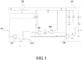
- Fig. 1 is a schematic diagram of a signal control circuit of a liquid crystal display panel according to an embodiment of the present disclosure.
- the present embodiment is able to solve the problem.
- the present disclosure provides a signal control circuit of a liquid crystal display panel.
- the signal control circuit includes a pulse width modulation module 101, a voltage-dividing module, and a switching transistor Q1.
- An input terminal of the voltage-dividing module is connected to receive a control signal.
- An output terminal of the voltage-dividing module is connected to an input terminal of the pulse width modulation module 101.
- the switching transistor Q1 is connected between an output terminal of the pulse width modulation module 101 and the input terminal of the voltage-dividing module.
- the pulse width modulation module 101 includes a selector and an amplifier.
- the voltage-dividing module includes a constant current driving sub-module 102 and a constant voltage driving sub-module 103.
- the constant current driving sub-module 102 includes an inductor L1, a diode D1, a first resistor R1, a subtractor 104, and a first amplifier 105 that are connected in series.
- An input terminal of the inductor LI is connected to receive the control signal.
- An input terminal of the first resistor R1 is connected to a first input terminal of the subtractor 104.
- An output terminal of the first resistor R1 is connected to a second input terminal of the subtractor 104.
- An output terminal of the subtractor 104 is connected to a first input terminal of the first amplifier 105.
- a second input terminal of the first amplifier 105 is configured to receive a first reference voltage Vref1.
- An output terminal of the first amplifier 105 is connected to a first input terminal of the selector 1011.
- the constant voltage driving sub-module 103 includes a second resistor R2, a third resistor R3, a fourth resistor R4, and a second amplifier 106 that are connected in series.
- An input terminal of the second resistor R2 is connected to the output terminal of the first resistor R1.
- An output terminal of the fourth resistor R4 is grounded.
- An output terminal of the third resistor R3 is connected to a first input terminal of the second amplifier 106.
- a second input terminal of the second amplifier 106 is configured to receive a second reference voltage Vref2.
- An output terminal of the second amplifier 106 is connected to a second input terminal of the selector 1011.
- a first capacitor C1 and a second capacitor C2 are provided between the output terminal of the first resistor R1 and the input terminal of the second resistor R2. One terminal of the first capacitor C1 and one terminal of the second capacitor C2 are grounded.
- a third amplifier 107 is provided between the selector 1011 and the switching transistor Q1.
- a first input terminal of the third amplifier 107 is connected to an output terminal of the selector 1011.
- a second input terminal of the third amplifier 107 is grounded.
- An output terminal of the third amplifier 107 is connected to a control terminal of the switching transistor Q1.
- the selector 1011 receives the fourth voltage V4 output by the constant current driving sub-module 102 and the fourth voltage V4 output by the constant voltage driving sub-module 103.
- the selector 1011 selects a voltage according to a booting time for outputting to the third amplifier 107.
- the third amplifier 107 then outputs a control signal after operation.
- the control signal determines a duty ratio of the switching transistor Q1, wherein when the duty ratio of the switching transistor Q1 is greater than 50%, the constant current driving sub-module 102 is activated; when the duty ratio of the switching transistor Q1 is lower than 50%, the constant voltage driving sub-module 103 is activated.
- a threshold value of the booting time may be set up so that the constant current driving sub-module is selected to be activated before the threshold value of the booting time, or the constant voltage driving sub-module is selected to be activated after the threshold value of the booting time.
- the driving circuit When booting, the driving circuit is activated under a constant current driving mode such that the liquid crystal display panel can be booted normally. After booting, the driving circuit changes to a constant current driving mode so as to drive the liquid crystal display panel to display images normally.
- a liquid crystal display panel is further provided and comprises a display panel body and a signal control circuit.
- the signal control circuit includes a pulse width modulation module, a voltage-dividing module, and a switching transistor.
- An input terminal of the voltage-dividing module is connected to receive a control signal.
- An output terminal of the voltage-dividing module is connected to an input terminal of the pulse width modulation module.
- the switching transistor is connected between an output terminal of the pulse width modulation module and the input terminal of the voltage-dividing module.
- the pulse width modulation module at least includes a selector.
- the voltage-dividing module includes: a constant current driving sub-module configured to provide a first voltage; and a constant voltage driving sub-module configured to provide a second voltage.
- the constant current driving sub-module and the constant voltage driving sub-module are selectively activated; wherein the selector is configured to select the first voltage or the second voltage to control a duty ratio of the switching transistor according to a booting time of the liquid crystal display panel, so as to further selectively activate the constant current driving sub-module or the constant voltage driving sub-module.
- the working principle of the liquid crystal display panel of the present preferred embodiment is identical to the working principle of the signal control circuit of a liquid crystal display panel of the foregoing preferred embodiment, and therefore it can be specifically referred to the working principle of the signal control circuit of the foregoing preferred embodiment and will not described in detail again to avoid redundancy.
- An advantage of the present disclosure is that: compared with a conventional signal control circuit of a liquid crystal display panel, the signal control circuit of the present disclosure, by activating a constant current mode during booting, can prevent a booting voltage from being pulled into a protection status that leads to incapability of booting.
- a technical problem existing in a conventional signal control circuit of a liquid crystal display panel where an inductor of the signal control circuit may generate large electric current at the moment of booting, thereby resulting in an overcurrent protection that causes electric current to be restricted and unable to normally turn on the liquid crystal display panel is solved.
Landscapes
- Engineering & Computer Science (AREA)
- Chemical & Material Sciences (AREA)
- Crystallography & Structural Chemistry (AREA)
- Physics & Mathematics (AREA)
- Computer Hardware Design (AREA)
- General Physics & Mathematics (AREA)
- Theoretical Computer Science (AREA)
- Power Engineering (AREA)
- Control Of Indicators Other Than Cathode Ray Tubes (AREA)
- Liquid Crystal Display Device Control (AREA)
- Dc-Dc Converters (AREA)
Abstract
Description
- The present disclosure relates to the technical field of liquid crystal displays, and more particularly to a signal control circuit and a liquid crystal display panel having the signal control circuit.
- In the past few years, while liquid crystal display panels are getting larger in size, electric current drawn from each channel in a driving circuit of a liquid crystal display panel is also getting larger, and a proportion of voltage ripple in the driving circuit is specifically restricted as well. Thus, capacitors for regulating voltages are also made larger.
- For each capacitor for regulating voltage, each capacitor needs to be charged during booting of a liquid crystal display panel. Because each capacitor has a large capacitance, and each current convertor has not yet reached a predetermined voltage when booting and a duty ratio of signals is relatively small, large electric current is then generated, thereby leading to a sharp increasing of inductive current, causing it to be hard for an output voltage to reach a predetermined value, and resulting in a wrong overcurrent protection for the driving circuit.
- In conclusion, in a conventional signal control circuit of a liquid crystal display panel, an inductor of the signal control circuit may generate large electric current at the moment of booting, thereby resulting in an overcurrent protection that causes electric current to be restricted and unable to normally turn on the liquid crystal display panel.
- The present disclosure provides a signal control circuit of a liquid crystal display panel that is able to avoid that the liquid crystal display panel cannot be normally turned on because the overcurrent protection is wrongly started during booting, thereby solving a technical problem existing in a conventional signal control circuit of a liquid crystal display panel where an inductor of the signal control circuit may generate large electric current at the moment of booting, thereby resulting in an overcurrent protection that causes electric current to be restricted and unable to normally turn on the liquid crystal display panel.
- In order to solve the foregoing problem, the present disclosure provides a technical solution as follows:
- a signal control circuit of a liquid crystal display panel includes a pulse width modulation module, a voltage-dividing module, and a switching transistor;
- an input terminal of the voltage-dividing module is connected to receive a control signal; an output terminal of the voltage-dividing module is connected to an input terminal of the pulse width modulation module; the switching transistor is connected between an output terminal of the pulse width modulation module and the input terminal of the voltage-dividing module;
- the pulse width modulation module at least includes a selector;
- the voltage-dividing module includes:
- a constant current driving sub-module configured to provide a first voltage; and
- a constant voltage driving sub-module configured to provide a second voltage;
- a third amplifier is provided between the selector and the switching transistor; a first input terminal of the third amplifier is connected to an output terminal of the selector; a second input terminal of the third amplifier is grounded; an output terminal of the third amplifier is connected to a control terminal of the switching transistor;
- the constant current driving sub-module and the constant voltage driving sub-module are selectively activated;
- wherein the selector is configured to select the first voltage or the second voltage to control a duty ratio of the switching transistor according to a booting time of the liquid crystal display panel, so as to further selectively activate the constant current driving sub-module or the constant voltage driving sub-module.
- According to a preferred embodiment of the present disclosure, the voltage-dividing module further includes a voltage-dividing terminal that is connected to a level converting module.
- According to a preferred embodiment of the present disclosure, the constant current driving sub-module includes an inductor, a diode, a first resistor, a subtractor, and a first amplifier that are connected in series; an input terminal of the inductor is connected to receive the control signal;
an input terminal of the first resistor is connected to a first input terminal of the subtractor; an output terminal of the first resistor is connected to a second input terminal of the subtractor; an output terminal of the subtractor is connected to a first input terminal of the first amplifier; a second input terminal of the first amplifier is configured to receive a first reference voltage; an output terminal of the first amplifier is connected to a first input terminal of the selector. - According to a preferred embodiment of the present disclosure, the constant voltage driving sub-module includes a second resistor, a third resistor, a fourth resistor, and a second amplifier that are connected in series;
an input terminal of the second resistor is connected to the output terminal of the first resistor; an output terminal of the fourth resistor is grounded; an output terminal of the third resistor is connected to a first input terminal of the second amplifier; a second input terminal of the second amplifier is configured to receive a second reference voltage; an output terminal of the second amplifier is connected to a second input terminal of the selector. - According to a preferred embodiment of the present disclosure, a first capacitor and a second capacitor are provided between the output terminal of the first resistor and an input terminal of the second resistor; one terminal of the first capacitor and one terminal of the second capacitor are grounded.
- The present disclosure further provides a signal control circuit of a liquid crystal display panel includes a pulse width modulation module, a voltage-dividing module, and a switching transistor;
an input terminal of the voltage-dividing module is connected to receive a control signal; an output terminal of the voltage-dividing module is connected to an input terminal of the pulse width modulation module; the switching transistor is connected between an output terminal of the pulse width modulation module and the input terminal of the voltage-dividing module;
the pulse width modulation module at least includes a selector;
the voltage-dividing module includes: - a constant current driving sub-module configured to provide a first voltage; and
- a constant voltage driving sub-module configured to provide a second voltage;
- the constant current driving sub-module and the constant voltage driving sub-module are selectively activated;
- the selector is configured to select the first voltage or the second voltage to control a duty ratio of the switching transistor according to a booting time of the liquid crystal display panel, so as to further selectively activate the constant current driving sub-module or the constant voltage driving sub-module.
- According to a preferred embodiment of the present disclosure, the voltage-dividing module further includes a voltage-dividing terminal that is connected to a level converting module.
- According to a preferred embodiment of the present disclosure, the constant current driving sub-module includes an inductor, a diode, a first resistor, a subtractor, and a first amplifier that are connected in series; an input terminal of the inductor is connected to receive the control signal;
an input terminal of the first resistor is connected to a first input terminal of the subtractor; an output terminal of the first resistor is connected to a second input terminal of the subtractor; an output terminal of the subtractor is connected to a first input terminal of the first amplifier; a second input terminal of the first amplifier is configured to receive a first reference voltage; an output terminal of the first amplifier is connected to a first input terminal of the selector. - According to a preferred embodiment of the present disclosure, the constant voltage driving sub-module includes a second resistor, a third resistor, a fourth resistor, and a second amplifier that are connected in series;
an input terminal of the second resistor is connected to the output terminal of the first resistor; an output terminal of the fourth resistor is grounded; an output terminal of the third resistor is connected to a first input terminal of the second amplifier; a second input terminal of the second amplifier is configured to receive a second reference voltage; an output terminal of the second amplifier is connected to a second input terminal of the selector. - According to a preferred embodiment of the present disclosure, a first capacitor and a second capacitor are provided between the output terminal of the first resistor and an input terminal of the second resistor; one terminal of the first capacitor and one terminal of the second capacitor are grounded.
- The present disclosure further provides a liquid crystal display panel including a display panel body and a signal control circuit. The signal control circuit includes a pulse width modulation module, a voltage-dividing module, and a switching transistor;
an input terminal of the voltage-dividing module is connected to receive a control signal; an output terminal of the voltage-dividing module is connected to an input terminal of the pulse width modulation module; the switching transistor is connected between an output terminal of the pulse width modulation module and the input terminal of the voltage-dividing module;
the pulse width modulation module at least includes a selector;
the voltage-dividing module includes: - a constant current driving sub-module configured to provide a first voltage; and
- a constant voltage driving sub-module configured to provide a second voltage;
- the constant current driving sub-module and the constant voltage driving sub-module are selectively activated;
- the selector is configured to select the first voltage or the second voltage to control a duty ratio of the switching transistor according to a booting time of the liquid crystal display panel, so as to further selectively activate the constant current driving sub-module or the constant voltage driving sub-module.
- According to a preferred embodiment of the present disclosure, the voltage-dividing module further includes a voltage-dividing terminal that is connected to a level converting module.
- According to a preferred embodiment of the present disclosure, the constant current driving sub-module includes an inductor, a diode, a first resistor, a subtractor, and a first amplifier that are connected in series; an input terminal of the inductor is connected to receive the control signal;
an input terminal of the first resistor is connected to a first input terminal of the subtractor; an output terminal of the first resistor is connected to a second input terminal of the subtractor; an output terminal of the subtractor is connected to a first input terminal of the first amplifier; a second input terminal of the first amplifier is configured to receive a first reference voltage; an output terminal of the first amplifier is connected to a first input terminal of the selector. - According to a preferred embodiment of the present disclosure, the constant voltage driving sub-module includes a second resistor, a third resistor, a fourth resistor, and a second amplifier that are connected in series;
an input terminal of the second resistor is connected to the output terminal of the first resistor; an output terminal of the fourth resistor is grounded; an output terminal of the third resistor is connected to a first input terminal of the second amplifier; a second input terminal of the second amplifier is configured to receive a second reference voltage; an output terminal of the second amplifier is connected to a second input terminal of the selector. - An advantage of the present disclosure is that:
compared with a conventional signal control circuit of a liquid crystal display panel, the signal control circuit of the present disclosure, by activating a constant current mode during booting, can prevent a booting voltage from being pulled into a protection status that leads to incapability of booting. Thus, a technical problem existing in a conventional signal control circuit of a liquid crystal display panel where an inductor of the signal control circuit may generates large electric current at the moment of booting, thereby resulting in an overcurrent protection that causes electric current to be restricted and unable to normally turn on the liquid crystal display panel is solved. - In order to explain the technical solutions in the present embodiments or in the prior art more clearly, accompanying drawings required in the description of the present embodiments or prior art will be briefly described. Obviously, accompanying drawings are just some embodiments of the present disclosure, while other drawings may be obtained by those skilled in the art according to these drawings, without making any creative effort.
-
Fig. 1 is a schematic diagram of a signal control circuit of a liquid crystal display panel according to an embodiment of the present disclosure. - The foregoing objects, features, and advantages adopted by the present disclosure can be best understood by referring to the following detailed description of the preferred embodiments and the accompanying drawings. Furthermore, the directional terms described in the present disclosure, such as upper, lower, front, rear, left, right, inner, outer, side, etc., are only directions referring to the accompanying drawings, so that the used directional terms are used to describe and understand the present disclosure, but the present disclosure is not limited thereto. In the drawings, similar structural units are designated by the same reference numerals.
- For a technical problem existing in a conventional signal control circuit of a liquid crystal display panel where an inductor of the signal control circuit may generates large electric current at the moment of booting, thereby resulting in an overcurrent protection that causes electric current to be restricted and unable to normally turn on the liquid crystal display panel, the present embodiment is able to solve the problem.
- As shown in
Fig. 1 , the present disclosure provides a signal control circuit of a liquid crystal display panel. The signal control circuit includes a pulsewidth modulation module 101, a voltage-dividing module, and a switching transistor Q1. An input terminal of the voltage-dividing module is connected to receive a control signal. An output terminal of the voltage-dividing module is connected to an input terminal of the pulse width modulation module 101.The switching transistor Q1 is connected between an output terminal of the pulsewidth modulation module 101 and the input terminal of the voltage-dividing module. - The pulse
width modulation module 101 includes a selector and an amplifier. The voltage-dividing module includes a constant current driving sub-module 102 and a constant voltage driving sub-module 103. - The constant current driving sub-module 102 includes an inductor L1, a diode D1, a first resistor R1, a
subtractor 104, and afirst amplifier 105 that are connected in series. An input terminal of the inductor LI is connected to receive the control signal. An input terminal of the first resistor R1 is connected to a first input terminal of thesubtractor 104. An output terminal of the first resistor R1 is connected to a second input terminal of thesubtractor 104. An output terminal of thesubtractor 104 is connected to a first input terminal of thefirst amplifier 105. A second input terminal of thefirst amplifier 105 is configured to receive a first reference voltage Vref1. An output terminal of thefirst amplifier 105 is connected to a first input terminal of theselector 1011. - After the control signal enters the signal control circuit, electric current is rectified by the inductor L1 and the diode D1 and then enters the first input terminal of the
subtractor 104 and the first resistor R1. After going through the first resistor R1, the electric current enters the second input terminal of thesubtractor 104, wherein the electric current that passes through the resistor R1 is relatively small. Thesubtractor 104 receives different electric current with the two input terminals and then outputs a first voltage V1 after calculation. The first voltage V1 enters the first input terminal of thefirst amplifier 105. Thefirst amplifier 105 outputs a fourth voltage V4 by operating and amplifying based on the first voltage V1 and the first reference voltage Vref1. The fourth voltage then enters the first input terminal of theselector 1011. - The constant voltage driving sub-module 103 includes a second resistor R2, a third resistor R3, a fourth resistor R4, and a
second amplifier 106 that are connected in series. An input terminal of the second resistor R2 is connected to the output terminal of the first resistor R1. An output terminal of the fourth resistor R4 is grounded. An output terminal of the third resistor R3 is connected to a first input terminal of thesecond amplifier 106. A second input terminal of thesecond amplifier 106 is configured to receive a second reference voltage Vref2. An output terminal of thesecond amplifier 106 is connected to a second input terminal of theselector 1011. - A first capacitor C1 and a second capacitor C2 are provided between the output terminal of the first resistor R1 and the input terminal of the second resistor R2. One terminal of the first capacitor C1 and one terminal of the second capacitor C2 are grounded.
- A
third amplifier 107 is provided between theselector 1011 and the switching transistor Q1. A first input terminal of thethird amplifier 107 is connected to an output terminal of theselector 1011. A second input terminal of thethird amplifier 107 is grounded. An output terminal of thethird amplifier 107 is connected to a control terminal of the switching transistor Q1. - After the control signal enters the signal control circuit, electric current orderly passes through the inductor LI, the diode D1, and the first resistor R1 and then charges the first capacitor C1 and the second capacitor C2 so that a voltage gradually increases. The second resistor R2, the third resistor R3, and the fourth resistor R4 constitute a constant-voltage mode. The third resistor R3 outputs a second voltage V2 to the first input terminal of the
second amplifier 106. Thesecond amplifier 106 outputs a third voltage V3 to the second input terminal of theselector 1011 by operating and amplifying based on the second voltage V2 and the second reference voltage Vref2. - The
selector 1011 receives the fourth voltage V4 output by the constant current driving sub-module 102 and the fourth voltage V4 output by the constant voltage driving sub-module 103. Theselector 1011 selects a voltage according to a booting time for outputting to thethird amplifier 107. Thethird amplifier 107 then outputs a control signal after operation. The control signal determines a duty ratio of the switching transistor Q1, wherein when the duty ratio of the switching transistor Q1 is greater than 50%, the constant current driving sub-module 102 is activated; when the duty ratio of the switching transistor Q1 is lower than 50%, the constant voltage driving sub-module 103 is activated. - For example, a threshold value of the booting time may be set up so that the constant current driving sub-module is selected to be activated before the threshold value of the booting time, or the constant voltage driving sub-module is selected to be activated after the threshold value of the booting time.
- When booting, the driving circuit is activated under a constant current driving mode such that the liquid crystal display panel can be booted normally. After booting, the driving circuit changes to a constant current driving mode so as to drive the liquid crystal display panel to display images normally.
- A liquid crystal display panel is further provided and comprises a display panel body and a signal control circuit. The signal control circuit includes a pulse width modulation module, a voltage-dividing module, and a switching transistor. An input terminal of the voltage-dividing module is connected to receive a control signal. An output terminal of the voltage-dividing module is connected to an input terminal of the pulse width modulation module. The switching transistor is connected between an output terminal of the pulse width modulation module and the input terminal of the voltage-dividing module. The pulse width modulation module at least includes a selector. The voltage-dividing module includes: a constant current driving sub-module configured to provide a first voltage; and a constant voltage driving sub-module configured to provide a second voltage. The constant current driving sub-module and the constant voltage driving sub-module are selectively activated; wherein the selector is configured to select the first voltage or the second voltage to control a duty ratio of the switching transistor according to a booting time of the liquid crystal display panel, so as to further selectively activate the constant current driving sub-module or the constant voltage driving sub-module.
- The working principle of the liquid crystal display panel of the present preferred embodiment is identical to the working principle of the signal control circuit of a liquid crystal display panel of the foregoing preferred embodiment, and therefore it can be specifically referred to the working principle of the signal control circuit of the foregoing preferred embodiment and will not described in detail again to avoid redundancy.
- An advantage of the present disclosure is that:
compared with a conventional signal control circuit of a liquid crystal display panel, the signal control circuit of the present disclosure, by activating a constant current mode during booting, can prevent a booting voltage from being pulled into a protection status that leads to incapability of booting. Thus, a technical problem existing in a conventional signal control circuit of a liquid crystal display panel where an inductor of the signal control circuit may generate large electric current at the moment of booting, thereby resulting in an overcurrent protection that causes electric current to be restricted and unable to normally turn on the liquid crystal display panel is solved. - In conclusion, although the present disclosure has been described with reference to the preferred embodiment thereof, it is apparent to those skilled in the art that a variety of modifications and changes may be made without departing from the scope of the present disclosure which is intended to be defined by the appended claims.
Claims (14)
- A signal control circuit of a liquid crystal display panel, comprising a pulse width modulation module, a voltage-dividing module, and a switching transistor;
wherein an input terminal of the voltage-dividing module is connected to receive a control signal; an output terminal of the voltage-dividing module is connected to an input terminal of the pulse width modulation module; the switching transistor is connected between an output terminal of the pulse width modulation module and the input terminal of the voltage-dividing module;
wherein the pulse width modulation module at least includes a selector;
wherein the voltage-dividing module includes:a constant current driving sub-module configured to provide a first voltage; anda constant voltage driving sub-module configured to provide a second voltage;wherein a third amplifier is provided between the selector and the switching transistor; a first input terminal of the third amplifier is connected to an output terminal of the selector; a second input terminal of the third amplifier is grounded; an output terminal of the third amplifier is connected to a control terminal of the switching transistor;wherein the constant current driving sub-module and the constant voltage driving sub-module are selectively activated;wherein the selector is configured to select the first voltage or the second voltage to control a duty ratio of the switching transistor according to a booting time of the liquid crystal display panel, so as to further selectively activate the constant current driving sub-module or the constant voltage driving sub-module. - The signal control circuit as claimed in claim 1, wherein the voltage-dividing module further includes a voltage-dividing terminal that is connected to a level converting module.
- The signal control circuit as claimed in claim 1, wherein the constant current driving sub-module includes an inductor, a diode, a first resistor, a subtractor, and a first amplifier that are connected in series; an input terminal of the inductor is connected to receive the control signal;
wherein an input terminal of the first resistor is connected to a first input terminal of the subtractor; an output terminal of the first resistor is connected to a second input terminal of the subtractor; an output terminal of the subtractor is connected to a first input terminal of the first amplifier; a second input terminal of the first amplifier is configured to receive a first reference voltage; an output terminal of the first amplifier is connected to a first input terminal of the selector. - The signal control circuit as claimed in claim 3, wherein the constant voltage driving sub-module includes a second resistor, a third resistor, a fourth resistor, and a second amplifier that are connected in series;
wherein an input terminal of the second resistor is connected to the output terminal of the first resistor; an output terminal of the fourth resistor is grounded; an output terminal of the third resistor is connected to a first input terminal of the second amplifier; a second input terminal of the second amplifier is configured to receive a second reference voltage; an output terminal of the second amplifier is connected to a second input terminal of the selector. - The signal control circuit as claimed in claim 4, wherein a first capacitor and a second capacitor are provided between the output terminal of the first resistor and the input terminal of the second resistor; one terminal of the first capacitor and one terminal of the second capacitor are grounded.
- A signal control circuit of a liquid crystal display panel, comprising a pulse width modulation module, a voltage-dividing module, and a switching transistor;
wherein an input terminal of the voltage-dividing module is connected to receive a control signal; an output terminal of the voltage-dividing module is connected to an input terminal of the pulse width modulation module; the switching transistor is connected between an output terminal of the pulse width modulation module and the input terminal of the voltage-dividing module;
wherein the pulse width modulation module at least includes a selector;
wherein the voltage-dividing module includes:a constant current driving sub-module configured to provide a first voltage; anda constant voltage driving sub-module configured to provide a second voltage;wherein the constant current driving sub-module and the constant voltage driving sub-module are selectively activated;wherein the selector is configured to select the first voltage or the second voltage to control a duty ratio of the switching transistor according to a booting time of the liquid crystal display panel, so as to further selectively activate the constant current driving sub-module or the constant voltage driving sub-module. - The signal control circuit as claimed in claim 6, wherein the voltage-dividing module further includes a voltage-dividing terminal that is connected to a level converting module.
- The signal control circuit as claimed in claim 6, wherein the constant current driving sub-module includes an inductor, a diode, a first resistor, a subtractor, and a first amplifier that are connected in series; an input terminal of the inductor is connected to receive the control signal;
wherein an input terminal of the first resistor is connected to a first input terminal of the subtractor; an output terminal of the first resistor is connected to a second input terminal of the subtractor; an output terminal of the subtractor is connected to a first input terminal of the first amplifier; a second input terminal of the first amplifier is configured to receive a first reference voltage; an output terminal of the first amplifier is connected to a first input terminal of the selector. - The signal control circuit as claimed in claim 8, wherein the constant voltage driving sub-module includes a second resistor, a third resistor, a fourth resistor, and a second amplifier that are connected in series;
wherein an input terminal of the second resistor is connected to the output terminal of the first resistor; an output terminal of the fourth resistor is grounded; an output terminal of the third resistor is connected to a first input terminal of the second amplifier; a second input terminal of the second amplifier is configured to receive a second reference voltage; an output terminal of the second amplifier is connected to a second input terminal of the selector. - The signal control circuit as claimed in claim 9, wherein a first capacitor and a second capacitor are provided between the output terminal of the first resistor and an input terminal of the second resistor; one terminal of the first capacitor and one terminal of the second capacitor are grounded.
- A liquid crystal display panel comprising a display panel body and a signal control circuit, wherein the signal control circuit includes a pulse width modulation module, a voltage-dividing module, and a switching transistor;
wherein an input terminal of the voltage-dividing module is connected to receive a control signal; an output terminal of the voltage-dividing module is connected to an input terminal of the pulse width modulation module; the switching transistor is connected between an output terminal of the pulse width modulation module and the input terminal of the voltage-dividing module;
wherein the pulse width modulation module at least includes a selector;
wherein the voltage-dividing module includes:a constant current driving sub-module configured to provide a first voltage; anda constant voltage driving sub-module configured to provide a second voltage;wherein the constant current driving sub-module and the constant voltage driving sub-module are selectively activated;wherein the selector is configured to select the first voltage or the second voltage to control a duty ratio of the switching transistor according to a booting time of the liquid crystal display panel, so as to further selectively activate the constant current driving sub-module or the constant voltage driving sub-module. - The liquid crystal display panel as claimed in claim 11, wherein the voltage-dividing module further includes a voltage-dividing terminal that is connected to a level converting module.
- The liquid crystal display panel as claimed in claim 11, wherein the constant current driving sub-module includes an inductor, a diode, a first resistor, a subtractor, and a first amplifier that are connected in series; an input terminal of the inductor is connected to receive the control signal;
wherein an input terminal of the first resistor is connected to a first input terminal of the subtractor; an output terminal of the first resistor is connected to a second input terminal of the subtractor; an output terminal of the subtractor is connected to a first input terminal of the first amplifier; a second input terminal of the first amplifier is configured to receive a first reference voltage; an output terminal of the first amplifier is connected to a first input terminal of the selector. - The liquid crystal display panel as claimed in claim 13, wherein the constant voltage driving sub-module includes a second resistor, a third resistor, a fourth resistor, and a second amplifier that are connected in series;
wherein an input terminal of the second resistor is connected to the output terminal of the first resistor; an output terminal of the fourth resistor is grounded; an output terminal of the third resistor is connected to a first input terminal of the second amplifier; a second input terminal of the second amplifier is configured to receive a second reference voltage; an output terminal of the second amplifier is connected to a second input terminal of the selector.
Applications Claiming Priority (2)
| Application Number | Priority Date | Filing Date | Title |
|---|---|---|---|
| CN201710592138.9A CN107369416B (en) | 2017-07-19 | 2017-07-19 | Liquid crystal display panel and its signal control circuit |
| PCT/CN2017/099392 WO2019015019A1 (en) | 2017-07-19 | 2017-08-29 | Liquid crystal display panel signal control circuit thereof |
Publications (2)
| Publication Number | Publication Date |
|---|---|
| EP3657488A1 true EP3657488A1 (en) | 2020-05-27 |
| EP3657488A4 EP3657488A4 (en) | 2021-03-24 |
Family
ID=60307306
Family Applications (1)
| Application Number | Title | Priority Date | Filing Date |
|---|---|---|---|
| EP17918306.6A Withdrawn EP3657488A4 (en) | 2017-07-19 | 2017-08-29 | Liquid crystal display panel signal control circuit thereof |
Country Status (5)
| Country | Link |
|---|---|
| EP (1) | EP3657488A4 (en) |
| JP (1) | JP6858923B2 (en) |
| KR (1) | KR102276809B1 (en) |
| CN (1) | CN107369416B (en) |
| WO (1) | WO2019015019A1 (en) |
Families Citing this family (2)
| Publication number | Priority date | Publication date | Assignee | Title |
|---|---|---|---|---|
| CN109346019B (en) * | 2018-11-22 | 2020-07-10 | 深圳市华星光电技术有限公司 | Overcurrent protection control circuit for level shift circuit |
| CN112636597B (en) * | 2020-12-03 | 2022-03-22 | 成都芯源系统有限公司 | Power management circuit, integrated circuit and overcurrent protection method thereof |
Family Cites Families (13)
| Publication number | Priority date | Publication date | Assignee | Title |
|---|---|---|---|---|
| US5266936A (en) * | 1989-05-09 | 1993-11-30 | Nec Corporation | Driving circuit for liquid crystal display |
| JPH11312592A (en) * | 1998-04-28 | 1999-11-09 | Canon Inc | Lamp control device and lamp control method |
| JP4809030B2 (en) * | 2005-09-28 | 2011-11-02 | 株式会社リコー | DRIVE CIRCUIT AND ELECTRONIC DEVICE USING THE DRIVE CIRCUIT |
| JP4869744B2 (en) * | 2006-03-09 | 2012-02-08 | 株式会社 日立ディスプレイズ | LED lighting device and liquid crystal display device using the same |
| US8022682B2 (en) * | 2006-05-01 | 2011-09-20 | International Rectifier Corporation | Method to reduce inrush voltage and current in a switching power converter |
| US7686508B2 (en) * | 2006-10-21 | 2010-03-30 | Intersil Americas Inc. | CMOS temperature-to-digital converter with digital correction |
| JP5076536B2 (en) * | 2007-02-16 | 2012-11-21 | 富士通セミコンダクター株式会社 | DC-DC conversion circuit, DC-DC conversion control circuit, and DC-DC conversion control method |
| JP2008228362A (en) * | 2007-03-08 | 2008-09-25 | Matsushita Electric Ind Co Ltd | Power supply |
| KR100867551B1 (en) * | 2007-05-18 | 2008-11-10 | 삼성전기주식회사 | LED array driving device |
| CN102624254B (en) * | 2012-03-26 | 2014-06-18 | 矽力杰半导体技术(杭州)有限公司 | Constant voltage constant current control circuit with improved load regulation and control method thereof |
| CN103177697B (en) * | 2013-03-15 | 2015-11-25 | 深圳市华星光电技术有限公司 | A kind of backlight drive circuit and backlight driving method, liquid crystal display |
| CN103281823B (en) * | 2013-05-08 | 2016-04-27 | 矽力杰半导体技术(杭州)有限公司 | There is the multiple power supplies system of constant current and constant voltage output |
| JP2017103966A (en) * | 2015-12-04 | 2017-06-08 | キヤノン株式会社 | Electronic apparatus |
-
2017
- 2017-07-19 CN CN201710592138.9A patent/CN107369416B/en active Active
- 2017-08-29 WO PCT/CN2017/099392 patent/WO2019015019A1/en not_active Ceased
- 2017-08-29 KR KR1020207004768A patent/KR102276809B1/en active Active
- 2017-08-29 EP EP17918306.6A patent/EP3657488A4/en not_active Withdrawn
- 2017-08-29 JP JP2020502264A patent/JP6858923B2/en active Active
Also Published As
| Publication number | Publication date |
|---|---|
| CN107369416A (en) | 2017-11-21 |
| JP2020527021A (en) | 2020-08-31 |
| JP6858923B2 (en) | 2021-04-14 |
| CN107369416B (en) | 2019-05-24 |
| EP3657488A4 (en) | 2021-03-24 |
| WO2019015019A1 (en) | 2019-01-24 |
| KR20200028463A (en) | 2020-03-16 |
| KR102276809B1 (en) | 2021-07-13 |
Similar Documents
| Publication | Publication Date | Title |
|---|---|---|
| US10401661B2 (en) | Method for manufacturing metal wire and array substrate using the same | |
| DE102012213359B4 (en) | CONTROL OF AN ELECTRONIC SWITCH | |
| US20090230873A1 (en) | Driving circuit for light emitting diodes | |
| US11189237B2 (en) | Current compensation circuit, virtual reality device and control method | |
| US9841649B2 (en) | Gate driver on array short-circuit protection circuit and liquid crystal panel including the same | |
| JP6442262B2 (en) | Voltage detection circuit | |
| US20160042678A1 (en) | Electronic paper apparatus and driving method thereof | |
| US9000624B2 (en) | Power-good signal generator and controller with power sequencing free | |
| US8922270B2 (en) | Charge pump and driver integrated circuit using the same | |
| CN107369416B (en) | Liquid crystal display panel and its signal control circuit | |
| US11087704B2 (en) | Liquid crystal panel driving circuit and liquid crystal panel | |
| US20080180418A1 (en) | Liquid crystal panel control circuit having reset circuit and liquid crystal display driving circuit with same | |
| EP3657490B1 (en) | Discharge signal triggering circuit and display device | |
| US20220124888A1 (en) | Buck topological circuit for power supply | |
| US10277135B2 (en) | Dual-output flyback voltage conversion circuit and display device | |
| JP2009253992A (en) | Switching supply circuit | |
| US9448572B2 (en) | Voltage adjusting circuit and all-in-one computer including the same | |
| EP4213384B1 (en) | Electronic device | |
| CN111028806A (en) | Gate drive circuit, liquid crystal panel, display device and aging method | |
| CN215870730U (en) | Overvoltage protection circuit | |
| US7965287B2 (en) | Power supply switching circuit capable of voltage regulation and flat panel display using same | |
| US11839006B2 (en) | Backlight control circuit, method for driving the same, backlight module and display apparatus | |
| CN221595166U (en) | Short circuit detection circuit, chip, display panel, electronic equipment | |
| TW201606739A (en) | Electronic paper apparatus and driving method thereof | |
| CN113870760B (en) | Gamma adjustment circuit and driving method |
Legal Events
| Date | Code | Title | Description |
|---|---|---|---|
| STAA | Information on the status of an ep patent application or granted ep patent |
Free format text: STATUS: THE INTERNATIONAL PUBLICATION HAS BEEN MADE |
|
| PUAI | Public reference made under article 153(3) epc to a published international application that has entered the european phase |
Free format text: ORIGINAL CODE: 0009012 |
|
| STAA | Information on the status of an ep patent application or granted ep patent |
Free format text: STATUS: REQUEST FOR EXAMINATION WAS MADE |
|
| 17P | Request for examination filed |
Effective date: 20200214 |
|
| AK | Designated contracting states |
Kind code of ref document: A1 Designated state(s): AL AT BE BG CH CY CZ DE DK EE ES FI FR GB GR HR HU IE IS IT LI LT LU LV MC MK MT NL NO PL PT RO RS SE SI SK SM TR |
|
| AX | Request for extension of the european patent |
Extension state: BA ME |
|
| DAV | Request for validation of the european patent (deleted) | ||
| DAX | Request for extension of the european patent (deleted) | ||
| A4 | Supplementary search report drawn up and despatched |
Effective date: 20210224 |
|
| RIC1 | Information provided on ipc code assigned before grant |
Ipc: G09G 3/36 20060101AFI20210218BHEP Ipc: H02M 3/156 20060101ALI20210218BHEP Ipc: H02M 1/36 20070101ALI20210218BHEP |
|
| STAA | Information on the status of an ep patent application or granted ep patent |
Free format text: STATUS: THE APPLICATION IS DEEMED TO BE WITHDRAWN |
|
| 18D | Application deemed to be withdrawn |
Effective date: 20210928 |