EP3656478A1 - Ultrasonic microintegrated mems acoustic transducer with reduced stress sensitivity and manufacturing process thereof - Google Patents
Ultrasonic microintegrated mems acoustic transducer with reduced stress sensitivity and manufacturing process thereof Download PDFInfo
- Publication number
- EP3656478A1 EP3656478A1 EP19210776.1A EP19210776A EP3656478A1 EP 3656478 A1 EP3656478 A1 EP 3656478A1 EP 19210776 A EP19210776 A EP 19210776A EP 3656478 A1 EP3656478 A1 EP 3656478A1
- Authority
- EP
- European Patent Office
- Prior art keywords
- cavity
- forming
- membrane
- sensitive portion
- wafer
- Prior art date
- Legal status (The legal status is an assumption and is not a legal conclusion. Google has not performed a legal analysis and makes no representation as to the accuracy of the status listed.)
- Granted
Links
Images





Classifications
-
- H—ELECTRICITY
- H04—ELECTRIC COMMUNICATION TECHNIQUE
- H04R—LOUDSPEAKERS, MICROPHONES, GRAMOPHONE PICK-UPS OR LIKE ACOUSTIC ELECTROMECHANICAL TRANSDUCERS; ELECTRIC HEARING AIDS; PUBLIC ADDRESS SYSTEMS
- H04R19/00—Electrostatic transducers
- H04R19/04—Microphones
-
- B—PERFORMING OPERATIONS; TRANSPORTING
- B06—GENERATING OR TRANSMITTING MECHANICAL VIBRATIONS IN GENERAL
- B06B—METHODS OR APPARATUS FOR GENERATING OR TRANSMITTING MECHANICAL VIBRATIONS OF INFRASONIC, SONIC, OR ULTRASONIC FREQUENCY, e.g. FOR PERFORMING MECHANICAL WORK IN GENERAL
- B06B1/00—Methods or apparatus for generating mechanical vibrations of infrasonic, sonic, or ultrasonic frequency
- B06B1/02—Methods or apparatus for generating mechanical vibrations of infrasonic, sonic, or ultrasonic frequency making use of electrical energy
- B06B1/06—Methods or apparatus for generating mechanical vibrations of infrasonic, sonic, or ultrasonic frequency making use of electrical energy operating with piezoelectric effect or with electrostriction
- B06B1/0644—Methods or apparatus for generating mechanical vibrations of infrasonic, sonic, or ultrasonic frequency making use of electrical energy operating with piezoelectric effect or with electrostriction using a single piezoelectric element
-
- B—PERFORMING OPERATIONS; TRANSPORTING
- B06—GENERATING OR TRANSMITTING MECHANICAL VIBRATIONS IN GENERAL
- B06B—METHODS OR APPARATUS FOR GENERATING OR TRANSMITTING MECHANICAL VIBRATIONS OF INFRASONIC, SONIC, OR ULTRASONIC FREQUENCY, e.g. FOR PERFORMING MECHANICAL WORK IN GENERAL
- B06B1/00—Methods or apparatus for generating mechanical vibrations of infrasonic, sonic, or ultrasonic frequency
- B06B1/02—Methods or apparatus for generating mechanical vibrations of infrasonic, sonic, or ultrasonic frequency making use of electrical energy
- B06B1/06—Methods or apparatus for generating mechanical vibrations of infrasonic, sonic, or ultrasonic frequency making use of electrical energy operating with piezoelectric effect or with electrostriction
- B06B1/0644—Methods or apparatus for generating mechanical vibrations of infrasonic, sonic, or ultrasonic frequency making use of electrical energy operating with piezoelectric effect or with electrostriction using a single piezoelectric element
- B06B1/0662—Methods or apparatus for generating mechanical vibrations of infrasonic, sonic, or ultrasonic frequency making use of electrical energy operating with piezoelectric effect or with electrostriction using a single piezoelectric element with an electrode on the sensitive surface
- B06B1/0681—Methods or apparatus for generating mechanical vibrations of infrasonic, sonic, or ultrasonic frequency making use of electrical energy operating with piezoelectric effect or with electrostriction using a single piezoelectric element with an electrode on the sensitive surface and a damping structure
-
- B—PERFORMING OPERATIONS; TRANSPORTING
- B06—GENERATING OR TRANSMITTING MECHANICAL VIBRATIONS IN GENERAL
- B06B—METHODS OR APPARATUS FOR GENERATING OR TRANSMITTING MECHANICAL VIBRATIONS OF INFRASONIC, SONIC, OR ULTRASONIC FREQUENCY, e.g. FOR PERFORMING MECHANICAL WORK IN GENERAL
- B06B1/00—Methods or apparatus for generating mechanical vibrations of infrasonic, sonic, or ultrasonic frequency
- B06B1/02—Methods or apparatus for generating mechanical vibrations of infrasonic, sonic, or ultrasonic frequency making use of electrical energy
- B06B1/06—Methods or apparatus for generating mechanical vibrations of infrasonic, sonic, or ultrasonic frequency making use of electrical energy operating with piezoelectric effect or with electrostriction
- B06B1/0644—Methods or apparatus for generating mechanical vibrations of infrasonic, sonic, or ultrasonic frequency making use of electrical energy operating with piezoelectric effect or with electrostriction using a single piezoelectric element
- B06B1/0651—Methods or apparatus for generating mechanical vibrations of infrasonic, sonic, or ultrasonic frequency making use of electrical energy operating with piezoelectric effect or with electrostriction using a single piezoelectric element of circular shape
-
- B—PERFORMING OPERATIONS; TRANSPORTING
- B06—GENERATING OR TRANSMITTING MECHANICAL VIBRATIONS IN GENERAL
- B06B—METHODS OR APPARATUS FOR GENERATING OR TRANSMITTING MECHANICAL VIBRATIONS OF INFRASONIC, SONIC, OR ULTRASONIC FREQUENCY, e.g. FOR PERFORMING MECHANICAL WORK IN GENERAL
- B06B1/00—Methods or apparatus for generating mechanical vibrations of infrasonic, sonic, or ultrasonic frequency
- B06B1/02—Methods or apparatus for generating mechanical vibrations of infrasonic, sonic, or ultrasonic frequency making use of electrical energy
- B06B1/06—Methods or apparatus for generating mechanical vibrations of infrasonic, sonic, or ultrasonic frequency making use of electrical energy operating with piezoelectric effect or with electrostriction
- B06B1/0644—Methods or apparatus for generating mechanical vibrations of infrasonic, sonic, or ultrasonic frequency making use of electrical energy operating with piezoelectric effect or with electrostriction using a single piezoelectric element
- B06B1/0662—Methods or apparatus for generating mechanical vibrations of infrasonic, sonic, or ultrasonic frequency making use of electrical energy operating with piezoelectric effect or with electrostriction using a single piezoelectric element with an electrode on the sensitive surface
- B06B1/0666—Methods or apparatus for generating mechanical vibrations of infrasonic, sonic, or ultrasonic frequency making use of electrical energy operating with piezoelectric effect or with electrostriction using a single piezoelectric element with an electrode on the sensitive surface used as a diaphragm
-
- B—PERFORMING OPERATIONS; TRANSPORTING
- B81—MICROSTRUCTURAL TECHNOLOGY
- B81B—MICROSTRUCTURAL DEVICES OR SYSTEMS, e.g. MICROMECHANICAL DEVICES
- B81B7/00—Microstructural systems ; Auxiliary parts of microstructural devices or systems
- B81B7/0009—Structural features, others than packages, for protecting a device against environmental influences
- B81B7/0016—Protection against shocks or vibrations, e.g. vibration damping
-
- B—PERFORMING OPERATIONS; TRANSPORTING
- B81—MICROSTRUCTURAL TECHNOLOGY
- B81C—PROCESSES OR APPARATUS SPECIALLY ADAPTED FOR THE MANUFACTURE OR TREATMENT OF MICROSTRUCTURAL DEVICES OR SYSTEMS
- B81C1/00—Manufacture or treatment of devices or systems in or on a substrate
- B81C1/00777—Preserve existing structures from alteration, e.g. temporary protection during manufacturing
- B81C1/00825—Protect against mechanical threats, e.g. against shocks, or residues
-
- G—PHYSICS
- G10—MUSICAL INSTRUMENTS; ACOUSTICS
- G10K—SOUND-PRODUCING DEVICES; METHODS OR DEVICES FOR PROTECTING AGAINST, OR FOR DAMPING, NOISE OR OTHER ACOUSTIC WAVES IN GENERAL; ACOUSTICS NOT OTHERWISE PROVIDED FOR
- G10K9/00—Devices in which sound is produced by vibrating a diaphragm or analogous element, e.g. fog horns, vehicle hooters or buzzers
- G10K9/12—Devices in which sound is produced by vibrating a diaphragm or analogous element, e.g. fog horns, vehicle hooters or buzzers electrically operated
- G10K9/122—Devices in which sound is produced by vibrating a diaphragm or analogous element, e.g. fog horns, vehicle hooters or buzzers electrically operated using piezoelectric driving means
-
- H—ELECTRICITY
- H04—ELECTRIC COMMUNICATION TECHNIQUE
- H04R—LOUDSPEAKERS, MICROPHONES, GRAMOPHONE PICK-UPS OR LIKE ACOUSTIC ELECTROMECHANICAL TRANSDUCERS; ELECTRIC HEARING AIDS; PUBLIC ADDRESS SYSTEMS
- H04R31/00—Apparatus or processes specially adapted for the manufacture of transducers or diaphragms therefor
-
- B—PERFORMING OPERATIONS; TRANSPORTING
- B81—MICROSTRUCTURAL TECHNOLOGY
- B81B—MICROSTRUCTURAL DEVICES OR SYSTEMS, e.g. MICROMECHANICAL DEVICES
- B81B2201/00—Specific applications of microelectromechanical systems
- B81B2201/02—Sensors
- B81B2201/0264—Pressure sensors
-
- B—PERFORMING OPERATIONS; TRANSPORTING
- B81—MICROSTRUCTURAL TECHNOLOGY
- B81B—MICROSTRUCTURAL DEVICES OR SYSTEMS, e.g. MICROMECHANICAL DEVICES
- B81B2201/00—Specific applications of microelectromechanical systems
- B81B2201/02—Sensors
- B81B2201/0271—Resonators; ultrasonic resonators
-
- B—PERFORMING OPERATIONS; TRANSPORTING
- B81—MICROSTRUCTURAL TECHNOLOGY
- B81B—MICROSTRUCTURAL DEVICES OR SYSTEMS, e.g. MICROMECHANICAL DEVICES
- B81B2203/00—Basic microelectromechanical structures
- B81B2203/01—Suspended structures, i.e. structures allowing a movement
- B81B2203/0127—Diaphragms, i.e. structures separating two media that can control the passage from one medium to another; Membranes, i.e. diaphragms with filtering function
-
- B—PERFORMING OPERATIONS; TRANSPORTING
- B81—MICROSTRUCTURAL TECHNOLOGY
- B81B—MICROSTRUCTURAL DEVICES OR SYSTEMS, e.g. MICROMECHANICAL DEVICES
- B81B2203/00—Basic microelectromechanical structures
- B81B2203/01—Suspended structures, i.e. structures allowing a movement
- B81B2203/0145—Flexible holders
- B81B2203/0163—Spring holders
-
- H—ELECTRICITY
- H10—SEMICONDUCTOR DEVICES; ELECTRIC SOLID-STATE DEVICES NOT OTHERWISE PROVIDED FOR
- H10N—ELECTRIC SOLID-STATE DEVICES NOT OTHERWISE PROVIDED FOR
- H10N30/00—Piezoelectric or electrostrictive devices
- H10N30/20—Piezoelectric or electrostrictive devices with electrical input and mechanical output, e.g. functioning as actuators or vibrators
- H10N30/204—Piezoelectric or electrostrictive devices with electrical input and mechanical output, e.g. functioning as actuators or vibrators using bending displacement, e.g. unimorph, bimorph or multimorph cantilever or membrane benders
- H10N30/2047—Membrane type
-
- H—ELECTRICITY
- H10—SEMICONDUCTOR DEVICES; ELECTRIC SOLID-STATE DEVICES NOT OTHERWISE PROVIDED FOR
- H10N—ELECTRIC SOLID-STATE DEVICES NOT OTHERWISE PROVIDED FOR
- H10N30/00—Piezoelectric or electrostrictive devices
- H10N30/30—Piezoelectric or electrostrictive devices with mechanical input and electrical output, e.g. functioning as generators or sensors
- H10N30/308—Membrane type
Definitions
- the present invention relates to an ultrasonic microintegrated acoustic transducer of a MEMS (MicroElectroMechanical System) type with reduced stress sensitivity and to the manufacturing process thereof.
- MEMS MicroElectroMechanical System
- MUTs Micromachined Ultrasonic Transducers
- CMUTs Capacitive Micromachined Ultrasonic Transducers
- PMUTs Piezoelectric Micromachined Ultrasonic Transducers
- FIG. 1 schematically shows a PMUT acoustic transducer 1 (in the following, referred to as transducer 1).
- the transducer 1 comprises a body 3, of semiconductor material (for example, silicon), having a first 3A and a second surface 3B.
- semiconductor material for example, silicon
- the body 3 has a cavity 5, extending in the body 3 from the second surface 3B; in particular, the cavity 5 is delimited, at the side, by a wall 5A and, at the top, by a bottom surface 5B.
- the body portion 3 delimited between the bottom surface 5B and the first surface 3A of the body 3 forms a membrane 7, which is thus monolithic with the body 3.
- a piezoelectric actuator 10 extends on the first surface 3A of the body 3; in particular, the piezoelectric actuator 10 is formed by a stack of layers.
- the stack of layers comprises a first electrode 12; a piezoelectric layer 13, for example of PZT (lead titanate zirconate, Pb [Zr x Ti 1 - x ] O 3 ) or aluminium nitride (AlN), which extends on the first electrode 12; and a second electrode 14, which extends on the piezoelectric layer 13.
- PZT lead titanate zirconate, Pb [Zr x Ti 1 - x ] O 3
- AlN aluminium nitride
- the transducer 1 is coupled, through a bonding layer 16 (for example, a glue or oxide), to a board 19 (e.g., a PCB, Printed-Circuit Board).
- a bonding layer 16 for example, a glue or oxide
- a board 19 e.g., a PCB, Printed-Circuit Board
- the transducer 1 can operate according to various operating modes, for example as emitter or receiver.
- a periodic potential difference is applied between the first and the second electrodes 12, 14 of the piezoelectric actuator 10 so as to generate a periodic deflection of the membrane 7 in a direction parallel to an axis Z of a cartesian reference system XYZ and generate an ultrasonic acoustic wave.
- the membrane 7 of the transducer 1 is deflected by an incident ultrasonic acoustic wave and generates a periodic mechanical stress in the piezoelectric layer 13.
- a periodic potential difference which can be read by a reading circuit (not illustrated) coupled to the transducer 1 is created between the first and the second electrodes 12, 14 of the piezoelectric actuator 10.
- One or more transducers of the type illustrated in Figure 1 can be used in various application fields.
- Figure 2 shows a sensing system 20 capable of determining the distance of an object that is at least in part reflecting, by measuring, in a per se known manner, a time of flight (ToF).
- the sensing system 20 uses two transducers 1 (respectively referred to as first transducer 21 and second transducer 23 in Figure 2 ), which operate, respectively, as emitter and receiver, and measures the time that elapses between emission of a first ultrasonic acoustic wave, generated by the first transducer 21, and reception, by the second transducer 23, of a second acoustic wave, generated by reflection of the first acoustic wave by the object to be measured, designated by 22.
- the first and the second acoustic transducers 21, 23 have a first resonance frequency f r1 and a second resonance frequency f r2 , respectively.
- the first transducer 21 is actuated in resonance conditions, i.e. it emits an ultrasonic acoustic wave Si (hereinafter defined as emitted wave Si) at its own first resonance frequency f r1 .
- emitted wave Si ultrasonic acoustic wave Si
- the emitted wave Si is reflected by the object 22 and generates a reflected wave S r , having, to a first approximation, the same oscillation frequency f r1 as the emitted wave Si.
- the reflected wave S r is detected by the second transducer 23 and transduced into an electrical output signal in a per se knonw manner.
- the sensing system 20 has high sensitivity and a high SNR (Signal-to-Noise Ratio), and the electrical output signal is amplified.
- the displacement induced on the membrane of the second transducer 23 is smaller and, consequently, the sensitivity is lower, the SNR is lower and the electrical output signal is reduced.
- the frequency offset ⁇ f may, for example, be due to the presence of undesirable periodic mechanical stresses on the membrane of the first transducer 21, which may cause undesirable deflections of the membrane. These mechanical stresses are due to various factors, such as temperature, humidity, bonding to a package, EWS (Electrical Wafer Sorting) testing, and bending phenomena.
- EWS Electro Mechanical Wafer Sorting
- PMUTs preferably operate in resonance conditions; consequently, the resonance frequency is an important parameter for the proper operation of a PMUT.
- the aim of the present invention is to provide an acoustic transducer and a manufacturing process thereof that overcomes at least the drawbacks of the prior art and, in particular, is less sensitive to stresses.
- an acoustic transducer and the manufacturing process thereof are provided, as defined in the attached claims.
- FIGS 3 and 4 schematically shows a transducer 30 of a PMUT type having a first and a second planar extension axes Si, S 2 , parallel, respectively, to an axis Y and an axis X of a cartesian reference system XYZ, and a 180°-rotational symmetry axis O (hereinafter also referred to as central axis O), extending parallel to an axis Z of the cartesian reference system XYZ.
- the transducer 30 has a rotational symmetry through 180°, i.e. for each element present in the structure, there exists a corresponding element of the same dimensions and shape arranged rotated through 180° about the central axis O.
- the transducer 30 comprises a body 32 of semiconductor material (for example of silicon), having a first surface 32A and a second surface 32B, opposite to one another.
- the body 32 houses a first cavity 34, having, for example, a quadrangular (e.g., rectangular) shape in top plan view ( Figure 3 ), the top surface whereof is arranged at a first depth T 1 from the first surface 32A in a direction parallel to the axis Z of the cartesian reference system XYZ and is parallel to a plane XY of the reference system XYZ; and a plurality of decoupling trenches 36 (four illustrated in Figure 3 ), extending from the first surface 32A as far as the first cavity 34.
- the first cavity 34 has a first length L 1 measured along the axis X of the cartesian reference system XYZ ( Figure 4 ).
- the decoupling trenches 36 are, for example, L-shaped in top plan view ( Figure 3 ) and laterally delimit a sensitive portion 38 of the body 32, extending over the first cavity 34.
- the sensitive portion 38 of the body 32 is separated from a peripheral portion 32' of the body 32 by the decoupling trenches 36 and by an underlying portion 32" of the body 32 via the cavity 34.
- the decoupling trenches 36 put the first cavity 34 in communication with the external environment.
- the decoupling trenches 36 laterally delimit between them a plurality of spring elements 40 (four illustrated in Figure 3 ).
- the spring elements 40 are, for example, L-shaped in top plan view ( Figure 3 ), support the sensitive portion 38, and connect it to the peripheral portion 32' of the body 32.
- the spring elements 40 here comprise a first, a second, a third and a fourth spring elements 40A-40D, each comprising a respective first arm 41A-41D and a respective second arm 43A-43D.
- the first and the second arms 41A-41D, 43A-43D are transverse (in particular, perpendicular) to one another.
- the first and third spring elements 40A, 40C are symmetrical one another through 180° about the central axis O, i.e. they can be obtained by rotating, for example, the first spring element 40A through 180° about the central axis O.
- the second and fourth spring elements 40B, 40D are symmetrical through 180° about the central axis O. Consequently, the spring elements 40A-40D are symmetrical in pairs with respect to the central axis O and are arranged to surround the sides of the sensitive portion 38.
- first arm 41A, 41C of the first and third spring elements 40A, 40C extends parallel to the axis X and is connected, at a respective first end 41A', 41C', to the sensitive portion 38.
- the second arm 43A, 43C of the first and third spring elements 40A, 40C extends parallel to the axis Y and is connected, at a first end 43A', 43C', to a second end 41A", 41C" of the respective first arm 41A, 41C and, at a second end 43A", 43C", to the peripheral portion 32'.
- the first arm 41B, 41D of the second and fourth spring elements 40B, 40D extends parallel to the axis Y and is connected, at a respective first end 41B', 41D', to the sensitive portion 38.
- the second arm 43B, 43D of the second and fourth spring elements 40B, 40D extends parallel to the axis X and is connected, at a first end 43B', 43D', to a second end 41B", 41D" of the respective second arm 41B, 43B and, at a second end 43B", 43D", to the peripheral portion 32'.
- the spring elements 40A-40D and the sensitive portion 38 have a thickness (along the axis Z), for example, of between 10 ⁇ m and 80 ⁇ m.
- the sensitive portion 38 has a top surface formed by the first surface 32A of the body 32 and a bottom surface 38B, and is delimited underneath by the first cavity 34 at the bottom surface 38B. Moreover, the sensitive portion 38 houses a second cavity 42, having, for example, a circular shape centred on the central axis O ( Figure 3 ) and extending underneath the first surface 32A of the body 32 starting from a second depth T 2 in a direction parallel to the axis Z. The second depth T 2 is smaller than the first depth T 1 of the first cavity 34.
- the second cavity 42 has a diameter L 2 smaller than the length L 1 of the first cavity 34; moreover, the first cavity 34 projects on all sides (in a plane parallel to the plane XY of the cartesian reference system XYZ) with respect to the second cavity 42.
- the sensitive portion 38 defines a membrane 45, delimited at the top by the first surface 32A of the body 32 and at the bottom by the second cavity 42.
- a ventilation hole 44 extends in the sensitive portion 38, from the first surface 32A of the body 32 as far as the second cavity 42 through the thickness of the membrane 45; in particular, the ventilation hole 44 has, for example, a circular shape in top plan view ( Figure 3 ) and is arranged along the central axis O.
- the ventilation hole 44 puts the second cavity 42 in communication with the external environment; in this way, it is possible to equalise the pressure acting on the membrane 45.
- a piezoelectric actuator 50 extends on the first surface 32A of the body 32, on top of the membrane 45.
- the piezoelectric actuator 50 is formed by a stack of layers, comprising a first electrode 51 (for example, of titanium, molybdenum, or platinum); a piezoelectric layer 52, for example of PZT or aluminium nitride (AlN), extending on the first electrode 51; and a second electrode 53 (for example, of TiW, an alloy of titanium and tungsten, or molybdenum), which extends on the piezoelectric layer 52.
- the piezoelectric actuator 50 has, for example, an annular shape centred on the central axis O; in particular, the piezoelectric actuator 50 surrounds the ventilation hole 44 at a distance therefrom.
- the first and the second electrodes 51, 53 of the piezoelectric actuator 50 are connected, through a first and a second conductive paths 55A, 55B (schematically illustrated in Figure 3 ), to a first and a second contact pads 60, 62, respectively, which are arranged in the peripheral portion 32' of the body 32.
- the first and the second conductive paths 55A, 55B are of conductive material, such as molybdenum (Mo), gold (Au), aluminium (Al), or an alloy of aluminium and copper (AlCu).
- the first and the second contact pads 60, 62 are also of conductive material, such as metal, e.g., gold (Au), aluminium (Al), or else an alloy of aluminium and copper (AlCu).
- first and the second conductive paths 55A, 55B extend over the second spring element 40B and pass through it until the first and the second contact pads 60, 62.
- the transducer 30 operates according to the operating modes described in the following.
- a periodic potential difference (having an oscillation frequency, for example, equal to a first frequency f') is applied between the first and the second electrodes 51, 53 of the piezoelectric actuator 50 so as to induce a periodic mechanical stress in the piezoelectric layer 52 at the first frequency f' and, thus, generate a periodic deflection of the membrane 45 in a direction parallel to the axis Z at the first frequency f'.
- the periodic deflection of the membrane 45 enables the transducer 30 to emit an acoustic wave, in particular an ultrasonic wave, thus operating as an emitter.
- the transducer 30 operates as a receiver of ultrasonic acoustic waves.
- the membrane 45 of the transducer 30 is periodically deflected as a result of an ultrasonic acoustic wave (with an oscillation frequency equal to a second frequency f"), coming from the external environment, incident upon the membrane 45.
- the periodic deflection of the membrane 45 at the second frequency f" generates a periodic mechanical stress in the piezoelectric layer 52 and, thus, a periodic potential difference between the first and the second electrodes 51, 53 of the piezoelectric actuator 50 at the second frequency f".
- the periodic potential difference between the first and the second electrodes 51, 53 can be read by a reading circuit (not illustrated) electrically coupled to the transducer 30.
- the first and the second frequencies f', f" correspond to the resonance frequency of the piezoelectric actuator 50.
- the present transducer 30 has a reduced sensitivity to the external stresses, in particular to mechanical stresses.
- the first cavity 34, the decoupling trenches 36 and the spring elements 40 enable decoupling of the sensitive portion 38 from the peripheral portion 32' and from the underlying portion 32" of the body 32, reducing the impact on the membrane 45 exerted by possible mechanical stresses in the portions 32' and 32", and consequent variation of the resonance frequency of the transducer 30.
- the mass and stiffness of the spring elements 40 are designed to define the dynamic behaviour and, thus, their resonance frequency.
- the spring elements 40 are designed so that their resonance frequency is lower than the resonance frequency of the membrane 45 (for example, by one or two decades) . In this way, it is possible to prevent energy transfer between the spring elements 40 and the sensitive portion 38, a transfer that could have an adverse effect on the deflection capacity of the membrane 45 (in particular, the oscillation amplitude of the membrane 45).
- the transducer 30 may also comprise just two spring elements opposite to one another with respect to the first or second planar extension axes S 1 , S 2 ; for example, with reference to Figures 3 and 4 , just the first and third spring elements 40A, 40C or, alternatively, the second and fourth spring elements 40B, 40D may be provided.
- the transducer may also comprise just one spring element.
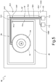
- Figure 5 shows a transducer 80 having a general structure similar to the transducer 30 of Figures 3-4 ; consequently, parts similar to the ones illustrated and described with reference to Figures 3-4 are designated in Figure 5 by the same reference numbers increased by 50 and will not be described any further.
- the transducer 80 here comprises the spring element 90A, similar to the first spring element 40A of the transducer 30 of Figures 3-4 .
- the transducer 30 of Figures 3-4 is manufactured as described hereinafter with reference to Figures 6-11 .
- a wafer 132 of monocrystalline silicon is machined so as to form the first buried cavity 34.
- the first buried cavity 34 may be formed in various ways, for example, as taught in European patent No. EP 1577656 .
- an epitaxial layer 133' of monocrystalline or polycrystalline silicon (represented by a dashed line in Figure 7 ) is grown on a face 132A of the wafer 132, designated in Figure 7 by 132'.
- the wafer 132' has a top face corresponding to the first surface 32A and a bottom face corresponding to the second surface 32B of the body 32 of Figures 3-4 .
- the wafer 132' is then machined so as to form the second buried cavity 42 of the transducer 30.
- the second buried cavity 42 may be formed in various ways, for example as taught in European patent No. EP 1577656 and, consequently, in a way similar to the first buried cavity 34.
- the membrane 45 of the transducer 30 is thus formed on the second buried cavity 34.
- the piezoelectric actuator 50 is formed on the top face 32A of the wafer 132' by depositing a stack of layers and defining them, in a known way.
- the conductive paths 55A, 55B are made, for example, of the same material of, and simultaneously with, one of the electrodes 51, 53, in a known way.
- the contact pads 60, 62 are formed.
- a first mask 244 of oxide (for example, of silicon oxide) is formed in a per se knonw manner.
- the first mask 244 has an opening 144 where it is desidered to subsequently form the ventilation hole 44.
- a second mask 344 for example a resist mask, is provided in a known way on the first mask 244 and in the ventilation opening 144.
- the first mask 244 and the wafer 132' are etched using a known anisotropic etching technique, for example, DRIE (Deep Reactive Ion Etch) until the first buried cavity 34.
- DRIE Deep Reactive Ion Etch
- the decoupling trenches 36 and the spring elements 40 are obtained.
- the second mask 344 is removed, and a further anisotropic etching is carried out from the top face 32A in depth as far as the second buried cavity 42. At the end of the etching, the membrane 45 and the ventilation hole 44 are obtained.
- the first mask 244 is removed in a per se knonw manner (for example, by wet etching with hydrofluoric acid, HF), and the wafer 132' is diced so as to obtain the transducer 30 of Figures 3-4 .
- the present manufacturing process can be used also for manufacturing the transducer 80 of Figure 5 ; to this end, the shape of the first and the second masks 244, 344 are modified to define the shape of the spring element 90A and of the decoupling trenches 86.
- Figure 12 shows another embodiment of the present transducer.
- Figure 12 shows a transducer 430 having a general structure similar to the MEMS pressure sensor 30 of Figures 3-4 .
- parts similar to the ones illustrated and described with reference to Figures 3-4 are designated in Figure 12 by the same reference numbers increased by 400 and will not be described any further.
- the body 432 comprises a first body portion 433' and a second body portion 433".
- first body portion 433' is delimited at the bottom by the second surface 432B and is traversed by a through cavity 480, laterally delimited by a first cavity wall 480A in the body 432.
- a dielectric layer 470 for example of silicon oxide (SiO 2 ) extends over the first body portion 433'.
- the second body portion 433" extends on the dielectric layer 470 and is delimited at the top by the first surface 432A.
- the second body portion 433" comprises the sensitive portion 438, the plurality of spring elements 440, as well as the peripheral portion 432' of the body 432.
- the second body portion 433" further comprises an anchorage element 483, having a closed shape (two portions whereof are visible in Figure 12 ) and extends towards the second body portion 433" through the dielectric layer 470; consequently, the anchorage element 483 has the same thickness as the intermediate layer 470 (measured along the axis Z) and here is monolithic with the first and the second body portions 433', 433".
- the dielectric layer 470 has a through opening 482 formed as a continuation of the through cavity 480, but having an greater area than the latter, so as to be recessed and offset with respect to the first cavity wall 480A of the first through cavity 480. Both the through cavity 480 and the through opening 482 have an area (in top plan view, parallel to the plane XY) greater than the sensitive portion 438, which is thus suspended over them.
- the sensitive portion 438 has, starting from its bottom surface 438B, a blind cavity 490, laterally delimited by a second cavity wall 490A in the sensitive portion 438 and, on its bottom wall, by the membrane 445.
- the blind cavity 490 is a continuation of the through cavity 480 and of the through opening 482.
- a recess 492 extends alongside the blind cavity 490, at the bottom wall of the latter, so as to be recessed with respect to the second cavity wall 490A.
- the transducer 430 of Figure 12 is manufactured as described hereinafter with reference to Figures 13-15 .
- the dielectric layer 470 (for example, of silicon oxide) is deposited and defined on a face 533A of a wafer 533 of monocrystalline silicon in a per se knonw manner; in particular, the dielectric layer 470 has first definition openings 572' and a second definition opening 572".
- a first structural layer 535 of monocrystalline or polycrystalline silicon is epitaxially grown on the dielectric layer 470.
- the first structural layer 535 fills the first definition openings 572', as well as the second definition opening 572".
- the anchorage element 483 is formed.
- a wafer 600 is obtained.
- a definition layer 575, of dielectric material (for example, of silicon oxide) is deposited and defined on a face 600A of the wafer 600 in a per se knonw manner.
- a third definition opening 577 and the ventilation opening 444 are formed.
- a second structural layer 537 of monocrystalline or polycrystalline silicon is epitaxially grown on the surface of the definition layer 575 and of the first structural layer 535.
- the second structural layer 535 fills the third definition opening 577, as well as the ventilation opening 444.
- a wafer 700 is obtained, comprising the first body portion 433', the dielectric layer 470, and the second body portion 433" and having a top face corresponding to the first surface 432A and a bottom face corresponding to the second surface 432B of the body 432.
- the stack of layers adapted to form the piezoelectric actuator 450 illustrated in Figure 12 is deposited on the first surface 432A in a way similar to what described with reference to Figure 8 .
- the wafer 700 is etched from the backside starting from the second surface 432B.
- a mask (not illustrated) is arranged on the second surface 432B and the wafer 700 is etched using a known etching technique (for example, dry etching).
- etching proceeds until the dielectric layer 470, to form the through cavity 480. Then, etching proceeds so as to remove the portions of semiconductor in the first definition openings 572' and in the second definition opening 572", as well as the underlying portions of the second body portion 433". In particular, in this step, the etch stops at the definition layer 575, thus forming the blind cavity 490, and proceeds elsewhere as far as the first surface 432A of the wafer 700, to form the ventilation hole 444 and the decoupling trenches 436, and define the sensitive portion 438 and the spring elements 440.
- the mask on the second surface 432B of the wafer 700 is removed, and the portions of the dielectric layer 470 and of the definition layer 575 exposed by the previous etching step are removed in a per se knonw manner (for example, by wet etching with hydrofluoric acid, HF), to release the membrane 445.
- the wafer 700 is then diced so as to obtain the transducer 430 of Figure 12 .
- transducers 30, 80, 430 of Figures 3-4 , 5 , and 12 can be used in systems of the type illustrated in Figure 2 and, in general, in any positioning and/or triangulation system, in a way similar to what has been discussed with reference to Figures 1 and 2 .
- the present acoustic transducer and the process thereof have several advantages.
- the spring elements are designed so as to decouple the sensitive portion (and thus the actuation membrane) from the rest of the body of the acoustic transducer and absorb existing mechanical stresses. In this way, the sensitive portion is physically and operatively isolated from the body of the acoustic transducer.
- multiple piezoelectric actuators may be arranged in the sensitive portion 38, 438 of the acoustic transducer of the type illustrated in Figures 3-5 and 12 so as to increase the acoustic power emitted per unit surface of the acoustic transducer.
- the sensitive portion 38, 438 of the acoustic transducer 30, 430 may comprise a pair of piezoelectric actuators 50, 450, each associated with a respective membrane 45, 445, to a respective second cavity 42, 442, and to a respective ventilation hole 44, 444.
- the piezoelectric actuators 50, 450 (as well as the respective membranes 45, 445, the respective second cavities 42, 442, and the respective ventilation holes, 44, 444) may be arranged alongside one another along the axis X and/or Y of the reference system XYZ, for example in a way symmetrical with respect to the central axis O.
Landscapes
- Engineering & Computer Science (AREA)
- Mechanical Engineering (AREA)
- Physics & Mathematics (AREA)
- Acoustics & Sound (AREA)
- Microelectronics & Electronic Packaging (AREA)
- Manufacturing & Machinery (AREA)
- Signal Processing (AREA)
- Health & Medical Sciences (AREA)
- Toxicology (AREA)
- Computer Hardware Design (AREA)
- General Health & Medical Sciences (AREA)
- Multimedia (AREA)
- Micromachines (AREA)
- Transducers For Ultrasonic Waves (AREA)
Abstract
Description
- The present invention relates to an ultrasonic microintegrated acoustic transducer of a MEMS (MicroElectroMechanical System) type with reduced stress sensitivity and to the manufacturing process thereof.
- Acoustic transducers obtained using the semiconductor technology, which operate according to a capacitive or piezoelectric principle for transduction of ultrasonic acoustic waves are known. In particular, these transducers are known as MUTs (Micromachined Ultrasonic Transducers) and may be either of a capacitive type (CMUTs, Capacitive Micromachined Ultrasonic Transducers) or of a piezoelectric type (PMUTs, Piezoelectric Micromachined Ultrasonic Transducers). In the following, reference will be made to PMUT acoustic transducers, without this, however, implying any loss of generality.
-
Figure 1 schematically shows a PMUT acoustic transducer 1 (in the following, referred to as transducer 1). - In particular, the
transducer 1 comprises abody 3, of semiconductor material (for example, silicon), having a first 3A and asecond surface 3B. - The
body 3 has acavity 5, extending in thebody 3 from thesecond surface 3B; in particular, thecavity 5 is delimited, at the side, by awall 5A and, at the top, by abottom surface 5B. Thebody portion 3 delimited between thebottom surface 5B and thefirst surface 3A of thebody 3 forms amembrane 7, which is thus monolithic with thebody 3. - A
piezoelectric actuator 10 extends on thefirst surface 3A of thebody 3; in particular, thepiezoelectric actuator 10 is formed by a stack of layers. In greater detail, the stack of layers comprises afirst electrode 12; apiezoelectric layer 13, for example of PZT (lead titanate zirconate, Pb [ZrxTi1-x] O3) or aluminium nitride (AlN), which extends on thefirst electrode 12; and asecond electrode 14, which extends on thepiezoelectric layer 13. - At the
second surface 3B of thebody 3, thetransducer 1 is coupled, through a bonding layer 16 (for example, a glue or oxide), to a board 19 (e.g., a PCB, Printed-Circuit Board). - In use, the
transducer 1 can operate according to various operating modes, for example as emitter or receiver. - When the
transducer 1 is used as emitter, a periodic potential difference is applied between the first and thesecond electrodes piezoelectric actuator 10 so as to generate a periodic deflection of themembrane 7 in a direction parallel to an axis Z of a cartesian reference system XYZ and generate an ultrasonic acoustic wave. - When the
transducer 1 is used as receiver, themembrane 7 of thetransducer 1 is deflected by an incident ultrasonic acoustic wave and generates a periodic mechanical stress in thepiezoelectric layer 13. Thus, a periodic potential difference which can be read by a reading circuit (not illustrated) coupled to thetransducer 1 is created between the first and thesecond electrodes piezoelectric actuator 10. - One or more transducers of the type illustrated in
Figure 1 can be used in various application fields. - For instance,
Figure 2 shows asensing system 20 capable of determining the distance of an object that is at least in part reflecting, by measuring, in a per se known manner, a time of flight (ToF). In practice, thesensing system 20 uses two transducers 1 (respectively referred to asfirst transducer 21 andsecond transducer 23 inFigure 2 ), which operate, respectively, as emitter and receiver, and measures the time that elapses between emission of a first ultrasonic acoustic wave, generated by thefirst transducer 21, and reception, by thesecond transducer 23, of a second acoustic wave, generated by reflection of the first acoustic wave by the object to be measured, designated by 22. - In the considered example, the first and the second
acoustic transducers first transducer 21 is actuated in resonance conditions, i.e. it emits an ultrasonic acoustic wave Si (hereinafter defined as emitted wave Si) at its own first resonance frequency fr1. In this way, the displacement of the membrane and the emitting power of thefirst transducer 21 are maximised. The emitted wave Si is reflected by theobject 22 and generates a reflected wave Sr, having, to a first approximation, the same oscillation frequency fr1 as the emitted wave Si. The reflected wave Sr is detected by thesecond transducer 23 and transduced into an electrical output signal in a per se knonw manner. - If the first resonance frequency fr1 is equal to the second resonance frequency fr2, the displacement of the membrane of the
second transducer 23, induced by the reflected wave Sr, is amplified; consequently, thesensing system 20 has high sensitivity and a high SNR (Signal-to-Noise Ratio), and the electrical output signal is amplified. - Instead, if the first and the second resonance frequencies fr1, fr2 are mismatched and a frequency offset Δf is present, the displacement induced on the membrane of the
second transducer 23 is smaller and, consequently, the sensitivity is lower, the SNR is lower and the electrical output signal is reduced. - The frequency offset Δf may, for example, be due to the presence of undesirable periodic mechanical stresses on the membrane of the
first transducer 21, which may cause undesirable deflections of the membrane. These mechanical stresses are due to various factors, such as temperature, humidity, bonding to a package, EWS (Electrical Wafer Sorting) testing, and bending phenomena. - Similar problems may arise in transducer systems of the type illustrated in
Figure 1 used for triangulation and mapping of the position of an object with respect to a reference space (for example, a three-dimensional space defined by the cartesian reference system XYZ). - Even in this case, PMUTs preferably operate in resonance conditions; consequently, the resonance frequency is an important parameter for the proper operation of a PMUT.
- The aim of the present invention is to provide an acoustic transducer and a manufacturing process thereof that overcomes at least the drawbacks of the prior art and, in particular, is less sensitive to stresses.
- According to the present invention, an acoustic transducer and the manufacturing process thereof are provided, as defined in the attached claims.
- For a better understanding of the present invention, preferred embodiments thereof are now described purely by way of non-limiting example, with reference to the attached drawings, wherein:
-
Figure 1 schematically shows an acoustic transducer of a known type; -
Figure 2 schematically shows a system for detecting an object of a known type; -
Figure 3 shows an embodiment of the present acoustic transducer in top plan view; -
Figure 4 shows a cross section, taken along the section line IV-IV, of the acoustic transducer ofFigure 3 ; -
Figure 5 shows another embodiment of the present acoustic transducer in top plan view; -
Figures 6-11 show successive steps of an embodiment of a manufacturing process of the acoustic transducer ofFigures 3-5 ; -
Figure 12 is a cross-sectional view, taken along the section line IV-IV ofFigure 3 , of a further embodiment of the present acoustic transducer; and -
Figures 13-15 show successive steps of another embodiment of the present manufacturing process of the acoustic transducer ofFigure 12 . -
Figures 3 and4 schematically shows atransducer 30 of a PMUT type having a first and a second planar extension axes Si, S2, parallel, respectively, to an axis Y and an axis X of a cartesian reference system XYZ, and a 180°-rotational symmetry axis O (hereinafter also referred to as central axis O), extending parallel to an axis Z of the cartesian reference system XYZ. In particular, in the illustrated embodiment, thetransducer 30 has a rotational symmetry through 180°, i.e. for each element present in the structure, there exists a corresponding element of the same dimensions and shape arranged rotated through 180° about the central axis O. - In particular,
Figure 4 , thetransducer 30 comprises abody 32 of semiconductor material (for example of silicon), having afirst surface 32A and asecond surface 32B, opposite to one another. - The
body 32 houses afirst cavity 34, having, for example, a quadrangular (e.g., rectangular) shape in top plan view (Figure 3 ), the top surface whereof is arranged at a first depth T1 from thefirst surface 32A in a direction parallel to the axis Z of the cartesian reference system XYZ and is parallel to a plane XY of the reference system XYZ; and a plurality of decoupling trenches 36 (four illustrated inFigure 3 ), extending from thefirst surface 32A as far as thefirst cavity 34. Moreover, thefirst cavity 34 has a first length L1 measured along the axis X of the cartesian reference system XYZ (Figure 4 ). - The
decoupling trenches 36 are, for example, L-shaped in top plan view (Figure 3 ) and laterally delimit asensitive portion 38 of thebody 32, extending over thefirst cavity 34. - In practice, the
sensitive portion 38 of thebody 32 is separated from a peripheral portion 32' of thebody 32 by thedecoupling trenches 36 and by anunderlying portion 32" of thebody 32 via thecavity 34. Thedecoupling trenches 36 put thefirst cavity 34 in communication with the external environment. - Moreover, the
decoupling trenches 36 laterally delimit between them a plurality of spring elements 40 (four illustrated inFigure 3 ). Thespring elements 40 are, for example, L-shaped in top plan view (Figure 3 ), support thesensitive portion 38, and connect it to the peripheral portion 32' of thebody 32. - The
spring elements 40 here comprise a first, a second, a third and afourth spring elements 40A-40D, each comprising a respectivefirst arm 41A-41D and a respectivesecond arm 43A-43D. The first and thesecond arms 41A-41D, 43A-43D are transverse (in particular, perpendicular) to one another. In particular, the first andthird spring elements first spring element 40A through 180° about the central axis O. Likewise, the second andfourth spring elements spring elements 40A-40D are symmetrical in pairs with respect to the central axis O and are arranged to surround the sides of thesensitive portion 38. - In greater detail, the
first arm third spring elements first end 41A', 41C', to thesensitive portion 38. Thesecond arm third spring elements first end 43A', 43C', to asecond end 41A", 41C" of the respectivefirst arm second end 43A", 43C", to the peripheral portion 32'. - The
first arm fourth spring elements first end 41B', 41D', to thesensitive portion 38. Thesecond arm fourth spring elements first end 43B', 43D', to asecond end 41B", 41D" of the respectivesecond arm second end 43B", 43D", to the peripheral portion 32'. - Moreover, the
spring elements 40A-40D and thesensitive portion 38 have a thickness (along the axis Z), for example, of between 10 µm and 80 µm. - The
sensitive portion 38 has a top surface formed by thefirst surface 32A of thebody 32 and abottom surface 38B, and is delimited underneath by thefirst cavity 34 at thebottom surface 38B. Moreover, thesensitive portion 38 houses asecond cavity 42, having, for example, a circular shape centred on the central axis O (Figure 3 ) and extending underneath thefirst surface 32A of thebody 32 starting from a second depth T2 in a direction parallel to the axis Z. The second depth T2 is smaller than the first depth T1 of thefirst cavity 34. Thesecond cavity 42 has a diameter L2 smaller than the length L1 of thefirst cavity 34; moreover, thefirst cavity 34 projects on all sides (in a plane parallel to the plane XY of the cartesian reference system XYZ) with respect to thesecond cavity 42. - The
sensitive portion 38 defines amembrane 45, delimited at the top by thefirst surface 32A of thebody 32 and at the bottom by thesecond cavity 42. - A
ventilation hole 44 extends in thesensitive portion 38, from thefirst surface 32A of thebody 32 as far as thesecond cavity 42 through the thickness of themembrane 45; in particular, theventilation hole 44 has, for example, a circular shape in top plan view (Figure 3 ) and is arranged along the central axis O. Theventilation hole 44 puts thesecond cavity 42 in communication with the external environment; in this way, it is possible to equalise the pressure acting on themembrane 45. - A
piezoelectric actuator 50 extends on thefirst surface 32A of thebody 32, on top of themembrane 45. In detail, thepiezoelectric actuator 50 is formed by a stack of layers, comprising a first electrode 51 (for example, of titanium, molybdenum, or platinum); apiezoelectric layer 52, for example of PZT or aluminium nitride (AlN), extending on thefirst electrode 51; and a second electrode 53 (for example, of TiW, an alloy of titanium and tungsten, or molybdenum), which extends on thepiezoelectric layer 52. Thepiezoelectric actuator 50 has, for example, an annular shape centred on the central axis O; in particular, thepiezoelectric actuator 50 surrounds theventilation hole 44 at a distance therefrom. - The first and the
second electrodes piezoelectric actuator 50 are connected, through a first and a secondconductive paths Figure 3 ), to a first and asecond contact pads body 32. In particular, the first and the secondconductive paths second contact pads - In the present embodiment, the first and the second
conductive paths second spring element 40B and pass through it until the first and thesecond contact pads - In use, the
transducer 30 operates according to the operating modes described in the following. - According to a first operating mode, a periodic potential difference (having an oscillation frequency, for example, equal to a first frequency f') is applied between the first and the
second electrodes piezoelectric actuator 50 so as to induce a periodic mechanical stress in thepiezoelectric layer 52 at the first frequency f' and, thus, generate a periodic deflection of themembrane 45 in a direction parallel to the axis Z at the first frequency f'. The periodic deflection of themembrane 45 enables thetransducer 30 to emit an acoustic wave, in particular an ultrasonic wave, thus operating as an emitter. - According to a second operating mode, the
transducer 30 operates as a receiver of ultrasonic acoustic waves. In this case, themembrane 45 of thetransducer 30 is periodically deflected as a result of an ultrasonic acoustic wave (with an oscillation frequency equal to a second frequency f"), coming from the external environment, incident upon themembrane 45. The periodic deflection of themembrane 45 at the second frequency f" generates a periodic mechanical stress in thepiezoelectric layer 52 and, thus, a periodic potential difference between the first and thesecond electrodes piezoelectric actuator 50 at the second frequency f". In particular, the periodic potential difference between the first and thesecond electrodes transducer 30. - In some operating modes, the first and the second frequencies f', f" correspond to the resonance frequency of the
piezoelectric actuator 50. - In both operating modes, the
present transducer 30 has a reduced sensitivity to the external stresses, in particular to mechanical stresses. - In fact, the
first cavity 34, thedecoupling trenches 36 and thespring elements 40 enable decoupling of thesensitive portion 38 from the peripheral portion 32' and from theunderlying portion 32" of thebody 32, reducing the impact on themembrane 45 exerted by possible mechanical stresses in theportions 32' and 32", and consequent variation of the resonance frequency of thetransducer 30. - In particular, the mass and stiffness of the
spring elements 40 are designed to define the dynamic behaviour and, thus, their resonance frequency. In greater detail, thespring elements 40 are designed so that their resonance frequency is lower than the resonance frequency of the membrane 45 (for example, by one or two decades) . In this way, it is possible to prevent energy transfer between thespring elements 40 and thesensitive portion 38, a transfer that could have an adverse effect on the deflection capacity of the membrane 45 (in particular, the oscillation amplitude of the membrane 45). - In other embodiments, the
transducer 30 may also comprise just two spring elements opposite to one another with respect to the first or second planar extension axes S1, S2; for example, with reference toFigures 3 and4 , just the first andthird spring elements fourth spring elements - In further embodiments, the transducer may also comprise just one spring element. On this regard,
Figure 5 shows atransducer 80 having a general structure similar to thetransducer 30 ofFigures 3-4 ; consequently, parts similar to the ones illustrated and described with reference toFigures 3-4 are designated inFigure 5 by the same reference numbers increased by 50 and will not be described any further. In particular, thetransducer 80 here comprises thespring element 90A, similar to thefirst spring element 40A of thetransducer 30 ofFigures 3-4 . - The
transducer 30 ofFigures 3-4 is manufactured as described hereinafter with reference toFigures 6-11 . - Initially,
Figure 6 , awafer 132 of monocrystalline silicon is machined so as to form the first buriedcavity 34. The first buriedcavity 34 may be formed in various ways, for example, as taught in European patent No.EP 1577656 . - Then,
Figure 7 , an epitaxial layer 133' of monocrystalline or polycrystalline silicon (represented by a dashed line inFigure 7 ) is grown on aface 132A of thewafer 132, designated inFigure 7 by 132'. In particular, the wafer 132' has a top face corresponding to thefirst surface 32A and a bottom face corresponding to thesecond surface 32B of thebody 32 ofFigures 3-4 . - The wafer 132' is then machined so as to form the second buried
cavity 42 of thetransducer 30. In particular, the second buriedcavity 42 may be formed in various ways, for example as taught in European patent No.EP 1577656 and, consequently, in a way similar to the first buriedcavity 34. - The
membrane 45 of thetransducer 30 is thus formed on the second buriedcavity 34. - Then,
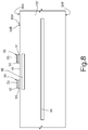
Figure 8 , thepiezoelectric actuator 50 is formed on thetop face 32A of the wafer 132' by depositing a stack of layers and defining them, in a known way. In this step, theconductive paths electrodes - Subsequently or simultaneously with the
conductive paths contact pads - Thereafter,
Figure 9 , afirst mask 244 of oxide (for example, of silicon oxide) is formed in a per se knonw manner. In particular, thefirst mask 244 has anopening 144 where it is desidered to subsequently form theventilation hole 44. - Next,
Figure 10 , asecond mask 344, for example a resist mask, is provided in a known way on thefirst mask 244 and in theventilation opening 144. - Using the
second mask 344, thefirst mask 244 and the wafer 132' are etched using a known anisotropic etching technique, for example, DRIE (Deep Reactive Ion Etch) until the first buriedcavity 34. At the end of the etching, thedecoupling trenches 36 and thespring elements 40 are obtained. - With reference to
Figure 11 , thesecond mask 344 is removed, and a further anisotropic etching is carried out from thetop face 32A in depth as far as the second buriedcavity 42. At the end of the etching, themembrane 45 and theventilation hole 44 are obtained. - Then, the
first mask 244 is removed in a per se knonw manner (for example, by wet etching with hydrofluoric acid, HF), and the wafer 132' is diced so as to obtain thetransducer 30 ofFigures 3-4 . - The present manufacturing process can be used also for manufacturing the
transducer 80 ofFigure 5 ; to this end, the shape of the first and thesecond masks spring element 90A and of thedecoupling trenches 86. -
Figure 12 shows another embodiment of the present transducer. In detail,Figure 12 shows atransducer 430 having a general structure similar to theMEMS pressure sensor 30 ofFigures 3-4 . Thus, parts similar to the ones illustrated and described with reference toFigures 3-4 are designated inFigure 12 by the same reference numbers increased by 400 and will not be described any further. - In
Figure 12 , thebody 432 comprises a first body portion 433' and asecond body portion 433". - In particular, the first body portion 433' is delimited at the bottom by the
second surface 432B and is traversed by a throughcavity 480, laterally delimited by afirst cavity wall 480A in thebody 432. - A
dielectric layer 470, for example of silicon oxide (SiO2) extends over the first body portion 433'. - The
second body portion 433" extends on thedielectric layer 470 and is delimited at the top by thefirst surface 432A. - In the present embodiment, the
second body portion 433" comprises thesensitive portion 438, the plurality ofspring elements 440, as well as the peripheral portion 432' of thebody 432. Thesecond body portion 433" further comprises ananchorage element 483, having a closed shape (two portions whereof are visible inFigure 12 ) and extends towards thesecond body portion 433" through thedielectric layer 470; consequently, theanchorage element 483 has the same thickness as the intermediate layer 470 (measured along the axis Z) and here is monolithic with the first and thesecond body portions 433', 433". - The
dielectric layer 470 has a throughopening 482 formed as a continuation of the throughcavity 480, but having an greater area than the latter, so as to be recessed and offset with respect to thefirst cavity wall 480A of the first throughcavity 480. Both the throughcavity 480 and the throughopening 482 have an area (in top plan view, parallel to the plane XY) greater than thesensitive portion 438, which is thus suspended over them. - The
sensitive portion 438 has, starting from itsbottom surface 438B, ablind cavity 490, laterally delimited by asecond cavity wall 490A in thesensitive portion 438 and, on its bottom wall, by themembrane 445. In detail, theblind cavity 490 is a continuation of the throughcavity 480 and of the throughopening 482. Arecess 492 extends alongside theblind cavity 490, at the bottom wall of the latter, so as to be recessed with respect to thesecond cavity wall 490A. - The
transducer 430 ofFigure 12 is manufactured as described hereinafter with reference toFigures 13-15 . - Initially,
Figure 13 , the dielectric layer 470 (for example, of silicon oxide) is deposited and defined on aface 533A of awafer 533 of monocrystalline silicon in a per se knonw manner; in particular, thedielectric layer 470 has first definition openings 572' and a second definition opening 572". - Then, a first
structural layer 535 of monocrystalline or polycrystalline silicon is epitaxially grown on thedielectric layer 470. In this step, the firststructural layer 535 fills the first definition openings 572', as well as the second definition opening 572". In particular, in this step, theanchorage element 483 is formed. At the end of the epitaxial growth of the firststructural layer 535, awafer 600 is obtained. - Next,
Figure 14 , adefinition layer 575, of dielectric material (for example, of silicon oxide) is deposited and defined on aface 600A of thewafer 600 in a per se knonw manner. In particular, athird definition opening 577 and theventilation opening 444 are formed. - Then, a second
structural layer 537 of monocrystalline or polycrystalline silicon is epitaxially grown on the surface of thedefinition layer 575 and of the firststructural layer 535. In particular, the secondstructural layer 535 fills thethird definition opening 577, as well as theventilation opening 444. At the end of the process of epitaxial growth of the secondstructural layer 537, awafer 700 is obtained, comprising the first body portion 433', thedielectric layer 470, and thesecond body portion 433" and having a top face corresponding to thefirst surface 432A and a bottom face corresponding to thesecond surface 432B of thebody 432. - Next, the stack of layers adapted to form the
piezoelectric actuator 450 illustrated inFigure 12 , as well as the first and the secondconductive paths first surface 432A in a way similar to what described with reference toFigure 8 . - Then, the
wafer 700 is etched from the backside starting from thesecond surface 432B. - In detail, a mask (not illustrated) is arranged on the
second surface 432B and thewafer 700 is etched using a known etching technique (for example, dry etching). - The etch proceeds until the
dielectric layer 470, to form the throughcavity 480. Then, etching proceeds so as to remove the portions of semiconductor in the first definition openings 572' and in the second definition opening 572", as well as the underlying portions of thesecond body portion 433". In particular, in this step, the etch stops at thedefinition layer 575, thus forming theblind cavity 490, and proceeds elsewhere as far as thefirst surface 432A of thewafer 700, to form theventilation hole 444 and thedecoupling trenches 436, and define thesensitive portion 438 and thespring elements 440. - Next, the mask on the
second surface 432B of thewafer 700 is removed, and the portions of thedielectric layer 470 and of thedefinition layer 575 exposed by the previous etching step are removed in a per se knonw manner (for example, by wet etching with hydrofluoric acid, HF), to release themembrane 445. Thewafer 700 is then diced so as to obtain thetransducer 430 ofFigure 12 . - The
transducers Figures 3-4 ,5 , and12 can be used in systems of the type illustrated inFigure 2 and, in general, in any positioning and/or triangulation system, in a way similar to what has been discussed with reference toFigures 1 and 2 . - The present acoustic transducer and the process thereof have several advantages.
- In particular, the spring elements are designed so as to decouple the sensitive portion (and thus the actuation membrane) from the rest of the body of the acoustic transducer and absorb existing mechanical stresses. In this way, the sensitive portion is physically and operatively isolated from the body of the acoustic transducer.
- Reduction of the impact of the mechanical stresses on the sensitive portion thus enables a significant reduction of the frequency offset due to the mechanical stresses in the present acoustic transducer. Consequently, when the present acoustic transducer operates, for example, as an emitter in resonance conditions (and thus the membrane vibrates at the resonance frequency), the emitted ultrasonic acoustic wave will have a frequency substantially equal to the resonance frequency of the acoustic transducer. This advantage is particularly useful in emitter-receiver systems of the type illustrated in
Figure 2 and/or in generic positioning/triangulation systems that include a multiplicity of acoustic transducers of the type illustrated inFigures 3-5 and12 . - Finally, it is clear that modifications and variations may be made to the MEMS device and to the manufacturing process described and illustrated herein, without thereby departing from the scope of the present invention, as defined in the attached claims.
- For instance, the various embodiments described may be combined so as to provide further solutions.
- Moreover, multiple piezoelectric actuators, as well as respective membranes, respective second cavities, and respective ventilation holes, may be arranged in the
sensitive portion Figures 3-5 and12 so as to increase the acoustic power emitted per unit surface of the acoustic transducer. For instance, thesensitive portion acoustic transducer piezoelectric actuators respective membrane second cavity 42, 442, and to arespective ventilation hole piezoelectric actuators 50, 450 (as well as therespective membranes second cavities 42, 442, and the respective ventilation holes, 44, 444) may be arranged alongside one another along the axis X and/or Y of the reference system XYZ, for example in a way symmetrical with respect to the central axis O.
Claims (15)
- A microintegrated MEMS acoustic transducer (30; 80; 430) of an ultrasonic type comprising:a body (32; 82; 432, 433', 433") of semiconductor material, the body having a first and a second surface (32A, 32B; 82A; 432A, 432B) opposite to each other;a first cavity (34; 84; 480), extending in the body;a sensitive portion (38; 88; 438), suspended over the first cavity and extending between the first cavity and the first surface of the body, the sensitive portion housing a second cavity (42; 92; 490), the sensitive portion comprising a membrane (45; 95; 445) extending between the second cavity and the first surface of the body;a piezoelectric actuator (50; 100; 450) extending over the membrane; andan elastic supporting structure (40, 40A-40D; 90, 90A; 440, 440A, 440C) extending between the sensitive portion and the body and is suspended over the first cavity.
- The transducer according to claim 1, further comprising:a peripheral portion (32'; 82'; 432'); andat least one decoupling trench (36; 86; 436), extending in the body from the first surface (32A; 82A; 432A) until the first cavity, the decoupling trench laterally delimiting the sensitive portion (38; 88; 438) and the elastic supporting structure (40, 40A-40D; 90, 90A; 440, 440A, 440C),wherein the elastic supporting structure is arranged between the sensitive portion and the peripheral portion.
- The transducer according to claim 2, wherein the elastic supporting structure (40, 40A-40D; 90, 90A; 440, 440A, 440C) comprises at least one spring element (40, 40A-40D; 90, 90A; 440, 440A, 440C) having an L-shape and comprising a first end and a second end (41A'-41D', 43A'-43D', 41A"-41D"; 91A', 93A', 91A", 93A"), the first end of the spring element being coupled to the sensitive portion (38; 88; 438); and the second end of the spring element being coupled to the peripheral portion (32'; 82'; 432') of the body (32; 82; 432, 433', 433").
- The transducer according to any of the preceding claims, wherein the elastic supporting structure (40, 40A-40D; 440, 440A, 440C) comprises a first (40A; 440A), a second (40B), a third (40C; 440C), and a fourth spring element (40D), surrounding the sensitive portion (38; 438), the first and the third spring elements being symmetrical through 180° with respect to a central axis (O) of the body (32; 82; 432, 433', 433"), the second and the fourth spring elements being symmetrical through 180° with respect to the central axis of the body and being rotated through 90° with respect to the first and the third spring elements, respectively.
- The transducer according to any of the preceding claims, wherein the membrane (45; 95; 445) has a ventilation hole (44; 94; 444) extending through the membrane until the second cavity (42; 92; 490).
- The transducer according to any of the preceding claims, wherein the first cavity (480) extends from the second surface of the body (432) until the sensitive portion and is laterally delimited by a first cavity wall (480A), the body further comprising a first body portion (433'), a second body portion (433") and an anchorage element (483), the anchorage element being arranged between the first and the second body portions in a recessed portion with respect to the first cavity wall and defining a through opening (482) offset with respect to the first cavity wall.
- The transducer according to claim 6, wherein the second cavity (490) extends between the membrane (445) and the first cavity and is laterally delimited by a second cavity wall (490A), the second cavity being in communication with the first cavity (480) and forming a recess (492) underneath the membrane (445), the recess being offset with respect to the second cavity wall.
- A process for manufacturing an ultrasonic microintegrated MEMS acoustic transducer, comprising:forming a first cavity (34; 84; 134; 480) in a semiconductor wafer (32; 82; 132; 132'; 432; 532; 600; 700), the semiconductor wafer having a first and a second surfaces (32A, 32B; 82A; 132A;432A, 432B; 532A; 600A; 700A, 700B);forming a second cavity (42; 92; 142; 490) in the semiconductor wafer between the first surface and the first cavity;forming a sensitive portion (38; 88; 438) and an elastic supporting structure (40, 40A-40D; 90, 90A; 440, 440A, 440C) in the semiconductor wafer over the first cavity, the elastic supporting structure carrying the sensitive portion, the sensitive portion including the second cavity and forming a membrane (45; 95; 445) between the second cavity and the first surface of the semiconductor wafer;forming a piezoelectric actuator (50; 100; 450) on the first surface (32A; 82A; 432A; 700A) of the semiconductor wafer extending over the membrane (32; 82; 132; 432; 700).
- The process according to claim 8, wherein forming the first cavity (34; 84) comprises:forming a first buried cavity (34; 84) in a work wafer (132) having a top surface (132A); andforming a first semiconductor layer (133') on the top surface of the work wafer so as to form an intermediate wafer (132') having a top surface forming the first surface (32A; 82A) of the semiconductor wafer (32; 82).
- The process according to claim 9, wherein forming the second cavity (42; 92) comprises:forming a second buried cavity (42; 92) in the intermediate wafer (132') on the first buried cavity (34); andforming a membrane layer (45; 95) on the top surface (32A; 82A) of the intermediate wafer, the membrane layer forming the membrane (45; 95).
- The process according to the claims 8 to 10, wherein forming the elastic supporting structure (40, 40A-40D; 90, 90A) comprises forming at least one decoupling trench (36; 86) in the semiconductor wafer (132) from the first surface (32A; 82A) of the semiconductor wafer, the decoupling trench extending until the first cavity (34; 84), laterally delimiting the sensitive portion (38; 88) and defining the elastic supporting structure.
- The process according to claim 8, wherein forming the first cavity (480) comprises:forming, on a top face (533A) of a work wafer (532), a first definition layer (470) having first and second openings (572', 572"); andforming, on the first definition layer, a first structural layer (535) filling the first and the second openings to form an intermediate wafer (600) having a top face (600A).
- The process according to claim 12, wherein forming the second cavity (490) comprises:forming, on the top face (600A) of the intermediate wafer (600), a second definition layer (575) having third and fourth openings (577, 444); andforming, on the second definition layer, a second structural layer (537) filling the third and the fourth openings to form the semiconductor wafer (432).
- The process according to claim 13, further comprising the steps of:removing portions of the work wafer (700) so as to form the first cavity (480), the first cavity being laterally delimited by a first cavity wall (480A);removing the first definition layer (470) so as to define a through opening (482), offset with respect to the first cavity wall;removing portions of the first structural layer (535) so as to form the second cavity (490) above and in a continuation of the first cavity, the second cavity being laterally delimited by a second cavity wall (490A);removing portions of the second definition layer (575) so as to define a recess (492), offset with respect to the second cavity wall; andselectively removing the second structural layer to form a ventilation hole (444) extending between the first surface of the semiconductor wafer (700) and the second cavity.
- The process according to claims 12 to 14, wherein forming the elastic supporting structure (440, 440A, 440D) comprises removing portions of the second structural layer (537) from the second surface (432B) of the semiconductor wafer (432; 700) so as to form at least one decoupling trench (436) that extends as far as the first cavity (480) and laterally delimits the sensitive portion (438).
Applications Claiming Priority (1)
| Application Number | Priority Date | Filing Date | Title |
|---|---|---|---|
| IT201800010485 | 2018-11-21 |
Publications (2)
| Publication Number | Publication Date |
|---|---|
| EP3656478A1 true EP3656478A1 (en) | 2020-05-27 |
| EP3656478B1 EP3656478B1 (en) | 2023-06-14 |
Family
ID=65324504
Family Applications (1)
| Application Number | Title | Priority Date | Filing Date |
|---|---|---|---|
| EP19210776.1A Active EP3656478B1 (en) | 2018-11-21 | 2019-11-21 | Ultrasonic microintegrated mems acoustic transducer with reduced stress sensitivity and manufacturing process thereof |
Country Status (3)
| Country | Link |
|---|---|
| US (1) | US11865581B2 (en) |
| EP (1) | EP3656478B1 (en) |
| CN (2) | CN111212370B (en) |
Cited By (4)
| Publication number | Priority date | Publication date | Assignee | Title |
|---|---|---|---|---|
| US11560886B2 (en) | 2019-04-15 | 2023-01-24 | Stmicroelectronics S.R.L. | Micropump MEMS device for moving or ejecting a fluid, in particular microblower or flowmeter |
| US20230129720A1 (en) * | 2021-10-26 | 2023-04-27 | Stmicroelectronics S.R.L. | Micro-electro-mechanical device for transducing high-frequency acoustic waves in a propagation medium and manufacturing process thereof |
| IT202100029288A1 (en) * | 2021-11-19 | 2023-05-19 | St Microelectronics Srl | MEMS ULTRASONIC TRANSDUCER DEVICE WITH IMPROVED DAMPING OF THE OSCILLATIONS OF A DIAPHRAGM THEREOF, AND MANUFACTURING PROCEDURE THEREOF |
| US20230354714A1 (en) * | 2020-09-15 | 2023-11-02 | Robert Bosch Gmbh | Micromechanical component, sound transducer device, and method for producing a micromechanical component |
Families Citing this family (13)
| Publication number | Priority date | Publication date | Assignee | Title |
|---|---|---|---|---|
| EP3934275B1 (en) * | 2020-07-02 | 2025-07-23 | xMEMS Labs, Inc. | Package structure and methods of manufacturing sound producing chip, forming package structure and forming sound producing apparatus |
| US11884535B2 (en) * | 2020-07-11 | 2024-01-30 | xMEMS Labs, Inc. | Device, package structure and manufacturing method of device |
| US20220304659A1 (en) * | 2021-03-29 | 2022-09-29 | Exo Imaging, Inc. | Trenches for the reduction of cross-talk in mut arrays |
| US12486159B2 (en) | 2021-06-30 | 2025-12-02 | Exo Imaging, Inc. | Micro-machined ultrasound transducers with insulation layer and methods of manufacture |
| US11899143B2 (en) | 2021-07-12 | 2024-02-13 | Robert Bosch Gmbh | Ultrasound sensor array for parking assist systems |
| US12150384B2 (en) | 2021-07-12 | 2024-11-19 | Robert Bosch Gmbh | Ultrasound transducer with distributed cantilevers |
| US12256642B2 (en) | 2021-07-12 | 2025-03-18 | Robert Bosch Gmbh | Ultrasound transducer with distributed cantilevers |
| IT202100019718A1 (en) | 2021-07-23 | 2023-01-23 | St Microelectronics Srl | IMPROVED PROCESS FOR MANUFACTURING ELECTROACOUSTIC MODULES |
| US20230092132A1 (en) * | 2021-09-23 | 2023-03-23 | Texas Instruments Incorporated | Wafer level processing for microelectronic device package with cavity |
| CN116140172B (en) * | 2021-11-19 | 2026-01-30 | 意法半导体股份有限公司 | MEMS ultrasonic transducer device with improved membrane oscillation damping and its manufacturing process |
| IT202200018153A1 (en) * | 2022-09-05 | 2024-03-05 | St Microelectronics Srl | MEMS ULTRASONIC TRANSDUCER DEVICE AND ITS MANUFACTURING PROCESS |
| US12284480B2 (en) | 2022-12-14 | 2025-04-22 | Stmicroelectronics International N.V. | Transducer assembly with buried cavities and method of manufacturing the same |
| US12465948B2 (en) * | 2023-02-09 | 2025-11-11 | Stmicroelectronics International N.V. | PMUT array with presence of separate sensing small PZT on membranes edge |
Citations (6)
| Publication number | Priority date | Publication date | Assignee | Title |
|---|---|---|---|---|
| EP1577656A1 (en) | 2004-03-19 | 2005-09-21 | STMicroelectronics S.r.l. | Method for manufacturing a semiconductor pressure sensor |
| US20150001651A1 (en) * | 2013-06-28 | 2015-01-01 | Stmicroelectronics S.R.I. | Mems device having a suspended diaphragm and manufacturing process thereof |
| US20150001645A1 (en) * | 2013-06-28 | 2015-01-01 | Stmicroelectronics S.R.I. | Mems device incorporating a fluidic path, and manufacturing process thereof |
| US20170001857A1 (en) * | 2015-07-01 | 2017-01-05 | Samsung Electro-Mechanics Co., Ltd. | Sensor element and method of manufacturing the same |
| US20170021391A1 (en) * | 2014-10-02 | 2017-01-26 | Chirp Microsystems | Micromachined ultrasonic transducers with a slotted membrane structure |
| US20170144881A1 (en) * | 2015-11-19 | 2017-05-25 | Stmicroelectronics S.R.L. | Micro-electro-mechanical device having two buried cavities and manufacturing process thereof |
Family Cites Families (33)
| Publication number | Priority date | Publication date | Assignee | Title |
|---|---|---|---|---|
| JPH08201569A (en) | 1995-01-31 | 1996-08-09 | Toshiba Corp | Ultrasonic inspection equipment |
| JP3830843B2 (en) | 2002-03-28 | 2006-10-11 | 株式会社東芝 | Thin film piezoelectric resonator |
| JP2004304622A (en) | 2003-03-31 | 2004-10-28 | Fujitsu Media Device Kk | Surface acoustic wave device and method of manufacturing the same |
| JP3875240B2 (en) | 2004-03-31 | 2007-01-31 | 株式会社東芝 | Manufacturing method of electronic parts |
| US7344907B2 (en) | 2004-11-19 | 2008-03-18 | International Business Machines Corporation | Apparatus and methods for encapsulating microelectromechanical (MEM) devices on a wafer scale |
| CN1632546A (en) | 2004-12-24 | 2005-06-29 | 王世光 | Monolithic piezoelectric and ferroelectric crystal multifunctional dew point humidity sensor |
| EP2096448B1 (en) | 2005-01-25 | 2016-01-20 | STMicroelectronics Srl | Process for manufacturing a pressure-monitoring device provided with a triaxial piezoresistive accelerometer |
| US7187488B2 (en) | 2005-03-09 | 2007-03-06 | Advanced Numicro Systems, Inc. | Trimming a MEMS device to fine tune natural frequency |
| JP4641217B2 (en) * | 2005-06-08 | 2011-03-02 | 株式会社豊田中央研究所 | Microphone and manufacturing method thereof |
| ITTO20050478A1 (en) | 2005-07-12 | 2007-01-13 | St Microelectronics Srl | PROCEDURE FOR THE REALIZATION OF CAVITIES 'BURIED WITHIN A SEMICONDUCTOR BODY AND SEMICONDUCTOR BODY MADE THESE |
| EP1762925B1 (en) | 2005-09-09 | 2016-12-21 | STMicroelectronics Srl | Analog input device with integrated pressure sensor and electronic apparatus equipped with said input device. |
| US7767484B2 (en) | 2006-05-31 | 2010-08-03 | Georgia Tech Research Corporation | Method for sealing and backside releasing of microelectromechanical systems |
| KR100781467B1 (en) | 2006-07-13 | 2007-12-03 | 학교법인 포항공과대학교 | MEMS-based multi-cavity ultrasonic transducer for superdirectional ultrasonic distance measurement using parametric transmissive arrays in air |
| ITTO20070190A1 (en) | 2007-03-14 | 2008-09-15 | St Microelectronics Srl | PROCESS OF MANUFACTURING OF A MEMBRANE OF SEMICONDUCTOR MATERIAL INTEGRATED IN, AND ISOLATED ELECTRICALLY BY, A SUBSTRATE |
| ITMI20072099A1 (en) | 2007-10-30 | 2009-04-30 | St Microelectronics Srl | METHOD OF MANUFACTURE OF AN ELECTRONIC DEVICE INCLUDING MEMS ENCAPSED MOLDING DEVICES |
| JP2009182838A (en) | 2008-01-31 | 2009-08-13 | Kyoto Univ | Elastic wave transducer, elastic wave transducer array, ultrasonic probe, ultrasonic imaging device |
| US8796790B2 (en) | 2008-06-25 | 2014-08-05 | MCube Inc. | Method and structure of monolithetically integrated micromachined microphone using IC foundry-compatiable processes |
| JP2010098518A (en) | 2008-10-16 | 2010-04-30 | Rohm Co Ltd | Method of manufacturing mems sensor, and mems sensor |
| US8448494B2 (en) | 2008-12-30 | 2013-05-28 | Stmicroelectronics S.R.L. | Integrated electronic microbalance plus chemical sensor |
| EP2252077B1 (en) | 2009-05-11 | 2012-07-11 | STMicroelectronics Srl | Assembly of a capacitive acoustic transducer of the microelectromechanical type and package thereof |
| CN102665940B (en) | 2009-12-25 | 2015-08-12 | 株式会社村田制作所 | Ultrasonic vibration device |
| US8633553B2 (en) | 2010-07-26 | 2014-01-21 | Stmicroelectronics S.R.L. | Process for manufacturing a micromechanical structure having a buried area provided with a filter |
| DE102013206524A1 (en) | 2013-04-12 | 2014-10-16 | Robert Bosch Gmbh | Component, utility and method of manufacturing a device |
| US10605903B2 (en) | 2014-03-18 | 2020-03-31 | Duke University | pMUT array for ultrasonic imaging, and related apparatuses, systems, and methods |
| US9386380B2 (en) | 2014-10-27 | 2016-07-05 | Taiwan Semiconductor Manufacturing Co., Ltd. | Method for the integration of a microelectromechanical systems (MEMS) microphone device with a complementary metal-oxide-semiconductor (CMOS) device |
| US10150664B2 (en) | 2014-12-15 | 2018-12-11 | Taiwan Semiconductor Manufacturing Co., Ltd. | Microelectromechanical systems (MEMS) stopper structure for stiction improvement |
| US9738516B2 (en) | 2015-04-29 | 2017-08-22 | Taiwan Semiconductor Manufacturing Co., Ltd. | Structure to reduce backside silicon damage |
| ITUB20159497A1 (en) | 2015-12-24 | 2017-06-24 | St Microelectronics Srl | PIEZOELECTRIC MEMS DEVICE AND ITS MANUFACTURING PROCEDURE |
| ITUA20162174A1 (en) | 2016-03-31 | 2017-10-01 | St Microelectronics Srl | PROCESS OF MANUFACTURE OF A MEMS PRESSURE SENSOR AND RELATIVE MEMS PRESSURE SENSOR |
| US10618801B2 (en) | 2016-11-10 | 2020-04-14 | Taiwan Semiconductor Manufacturing Co., Ltd. | MEMS structure with bilayer stopper and method for forming the same |
| IT201600131844A1 (en) | 2016-12-28 | 2018-06-28 | St Microelectronics Srl | ULTRASONIC PIEZOELECTRIC TRANSDUCER (PMUT) AND PMUT MANUFACTURING METHOD |
| IT201800002952A1 (en) | 2018-02-22 | 2019-08-22 | St Microelectronics Srl | IMPROVED MICRO-MACHINED ULTRASONIC TRANSDUCER (MUT), MUT MANUFACTURING METHOD, AND MUT DESIGN METHOD |
| US12552660B2 (en) | 2021-10-26 | 2026-02-17 | Stmicroelectronics S.R.L. | Micro-electro-mechanical device for transducing high-frequency acoustic waves in a propagation medium and manufacturing process thereof |
-
2019
- 2019-11-14 US US16/684,289 patent/US11865581B2/en active Active
- 2019-11-20 CN CN201911143036.4A patent/CN111212370B/en active Active
- 2019-11-20 CN CN201922012732.3U patent/CN211063784U/en active Active
- 2019-11-21 EP EP19210776.1A patent/EP3656478B1/en active Active
Patent Citations (6)
| Publication number | Priority date | Publication date | Assignee | Title |
|---|---|---|---|---|
| EP1577656A1 (en) | 2004-03-19 | 2005-09-21 | STMicroelectronics S.r.l. | Method for manufacturing a semiconductor pressure sensor |
| US20150001651A1 (en) * | 2013-06-28 | 2015-01-01 | Stmicroelectronics S.R.I. | Mems device having a suspended diaphragm and manufacturing process thereof |
| US20150001645A1 (en) * | 2013-06-28 | 2015-01-01 | Stmicroelectronics S.R.I. | Mems device incorporating a fluidic path, and manufacturing process thereof |
| US20170021391A1 (en) * | 2014-10-02 | 2017-01-26 | Chirp Microsystems | Micromachined ultrasonic transducers with a slotted membrane structure |
| US20170001857A1 (en) * | 2015-07-01 | 2017-01-05 | Samsung Electro-Mechanics Co., Ltd. | Sensor element and method of manufacturing the same |
| US20170144881A1 (en) * | 2015-11-19 | 2017-05-25 | Stmicroelectronics S.R.L. | Micro-electro-mechanical device having two buried cavities and manufacturing process thereof |
Cited By (8)
| Publication number | Priority date | Publication date | Assignee | Title |
|---|---|---|---|---|
| US11560886B2 (en) | 2019-04-15 | 2023-01-24 | Stmicroelectronics S.R.L. | Micropump MEMS device for moving or ejecting a fluid, in particular microblower or flowmeter |
| US20230354714A1 (en) * | 2020-09-15 | 2023-11-02 | Robert Bosch Gmbh | Micromechanical component, sound transducer device, and method for producing a micromechanical component |
| US12628566B2 (en) * | 2020-09-15 | 2026-05-12 | Robert Bosch Gmbh | Micromechanical component, sound transducer device, and method for producing a micromechanical component |
| US20230129720A1 (en) * | 2021-10-26 | 2023-04-27 | Stmicroelectronics S.R.L. | Micro-electro-mechanical device for transducing high-frequency acoustic waves in a propagation medium and manufacturing process thereof |
| EP4173729A1 (en) * | 2021-10-26 | 2023-05-03 | STMicroelectronics S.r.l. | Micro-electro-mechanical device for transducing high-frequency acoustic waves in a propagation medium and manufacturing process thereof |
| US12552660B2 (en) * | 2021-10-26 | 2026-02-17 | Stmicroelectronics S.R.L. | Micro-electro-mechanical device for transducing high-frequency acoustic waves in a propagation medium and manufacturing process thereof |
| IT202100029288A1 (en) * | 2021-11-19 | 2023-05-19 | St Microelectronics Srl | MEMS ULTRASONIC TRANSDUCER DEVICE WITH IMPROVED DAMPING OF THE OSCILLATIONS OF A DIAPHRAGM THEREOF, AND MANUFACTURING PROCEDURE THEREOF |
| EP4183490A1 (en) | 2021-11-19 | 2023-05-24 | STMicroelectronics S.r.l. | Mems ultrasonic transducer device with improved damping of the oscillations of a membrane of the same, and manufacturing process of the same |
Also Published As
| Publication number | Publication date |
|---|---|
| CN111212370A (en) | 2020-05-29 |
| CN211063784U (en) | 2020-07-21 |
| US11865581B2 (en) | 2024-01-09 |
| CN111212370B (en) | 2022-06-21 |
| EP3656478B1 (en) | 2023-06-14 |
| US20200156114A1 (en) | 2020-05-21 |
Similar Documents
| Publication | Publication Date | Title |
|---|---|---|
| EP3656478B1 (en) | Ultrasonic microintegrated mems acoustic transducer with reduced stress sensitivity and manufacturing process thereof | |
| US11051113B2 (en) | Piezoelectric acoustic MEMS transducer and fabrication method thereof | |
| US11950511B2 (en) | Micromachined ultrasonic transducer (MUT), method for manufacturing the MUT, and method for designing the MUT | |
| US10576500B2 (en) | Piezoelectric micro-machined ultrasonic transducer (PMUT) and method for manufacturing the PMUT | |
| EP3809476A1 (en) | Transducer with improved piezoelectric arrangement, mems device comprising the transducer, and methods for manufacturing the transducer | |
| US10715930B2 (en) | System and method for an optical MEMS transducer | |
| EP4173729B1 (en) | Micro-electro-mechanical device for transducing high-frequency acoustic waves in a propagation medium and manufacturing process thereof | |
| CN101262958A (en) | Surface micro-machining process for manufacturing micro-machined capacitive ultrasonic sensor | |
| CN111013993B (en) | Piezoelectric ultrasonic transducer and method of manufacturing the same | |
| Horsley et al. | Piezoelectric micromachined ultrasonic transducers in consumer electronics: The next little thing? | |
| CN110681560A (en) | MEMS ultrasonic positioning sensor with Helmholtz resonator | |
| US12551927B2 (en) | Multi-frequency hybrid piezo actuation and capactive transducer | |
| Wang et al. | Low thermal budget surface micromachining process for piezoelectric micromachined ultrasonic transducer arrays with in-situ vacuum sealed cavities | |
| CN111246356B (en) | A MEMS structure and a method for forming the same | |
| CN221453218U (en) | Micro-electromechanical system ultrasonic transducer device | |
| CN115752818B (en) | Resonant pressure sensor and manufacturing method thereof | |
| Bosetti et al. | Single-Layer Corrugated Aluminum Nitride Membranes as Piezoelectric Micromachined Ultrasonic Transducers with Differential Readout and Actuation | |
| US20240075499A1 (en) | Mems ultrasonic transducer device and manufacturing process thereof | |
| EP4183490B1 (en) | Mems ultrasonic transducer device with improved damping of the oscillations of a membrane of the same, and manufacturing process of the same | |
| CN121107345A (en) | MEMS structure and its fabrication method, ultrasonic transducer unit | |
| WO2022220142A1 (en) | Ultrasonic transducer, distance measurement device, and method for manufacturing ultrasonic transducer | |
| KR100233829B1 (en) | Micro gyroscope and its manufacturing method and angular velocity measuring method using the same | |
| JP2010074538A (en) | Ultrasonic vibrator |
Legal Events
| Date | Code | Title | Description |
|---|---|---|---|
| PUAI | Public reference made under article 153(3) epc to a published international application that has entered the european phase |
Free format text: ORIGINAL CODE: 0009012 |
|
| STAA | Information on the status of an ep patent application or granted ep patent |
Free format text: STATUS: THE APPLICATION HAS BEEN PUBLISHED |
|
| AK | Designated contracting states |
Kind code of ref document: A1 Designated state(s): AL AT BE BG CH CY CZ DE DK EE ES FI FR GB GR HR HU IE IS IT LI LT LU LV MC MK MT NL NO PL PT RO RS SE SI SK SM TR |
|
| AX | Request for extension of the european patent |
Extension state: BA ME |
|
| STAA | Information on the status of an ep patent application or granted ep patent |
Free format text: STATUS: REQUEST FOR EXAMINATION WAS MADE |
|
| 17P | Request for examination filed |
Effective date: 20201126 |
|
| RBV | Designated contracting states (corrected) |
Designated state(s): AL AT BE BG CH CY CZ DE DK EE ES FI FR GB GR HR HU IE IS IT LI LT LU LV MC MK MT NL NO PL PT RO RS SE SI SK SM TR |
|
| STAA | Information on the status of an ep patent application or granted ep patent |
Free format text: STATUS: EXAMINATION IS IN PROGRESS |
|
| 17Q | First examination report despatched |
Effective date: 20220708 |
|
| GRAP | Despatch of communication of intention to grant a patent |
Free format text: ORIGINAL CODE: EPIDOSNIGR1 |
|
| STAA | Information on the status of an ep patent application or granted ep patent |
Free format text: STATUS: GRANT OF PATENT IS INTENDED |
|
| RIC1 | Information provided on ipc code assigned before grant |
Ipc: H01L 41/113 20060101ALI20221209BHEP Ipc: H01L 41/09 20060101ALI20221209BHEP Ipc: H01L 41/053 20060101ALI20221209BHEP Ipc: G10K 9/122 20060101ALI20221209BHEP Ipc: B06B 1/06 20060101AFI20221209BHEP |
|
| INTG | Intention to grant announced |
Effective date: 20230105 |
|
| GRAS | Grant fee paid |
Free format text: ORIGINAL CODE: EPIDOSNIGR3 |
|
| GRAA | (expected) grant |
Free format text: ORIGINAL CODE: 0009210 |
|
| STAA | Information on the status of an ep patent application or granted ep patent |
Free format text: STATUS: THE PATENT HAS BEEN GRANTED |
|
| AK | Designated contracting states |
Kind code of ref document: B1 Designated state(s): AL AT BE BG CH CY CZ DE DK EE ES FI FR GB GR HR HU IE IS IT LI LT LU LV MC MK MT NL NO PL PT RO RS SE SI SK SM TR |
|
| REG | Reference to a national code |
Ref country code: CH Ref legal event code: EP |
|
| REG | Reference to a national code |
Ref country code: DE Ref legal event code: R096 Ref document number: 602019030946 Country of ref document: DE |
|
| REG | Reference to a national code |
Ref country code: AT Ref legal event code: REF Ref document number: 1578845 Country of ref document: AT Kind code of ref document: T Effective date: 20230715 |
|
| REG | Reference to a national code |
Ref country code: LT Ref legal event code: MG9D |
|
| REG | Reference to a national code |
Ref country code: NL Ref legal event code: MP Effective date: 20230614 |
|
| PG25 | Lapsed in a contracting state [announced via postgrant information from national office to epo] |
Ref country code: SE Free format text: LAPSE BECAUSE OF FAILURE TO SUBMIT A TRANSLATION OF THE DESCRIPTION OR TO PAY THE FEE WITHIN THE PRESCRIBED TIME-LIMIT Effective date: 20230614 Ref country code: NO Free format text: LAPSE BECAUSE OF FAILURE TO SUBMIT A TRANSLATION OF THE DESCRIPTION OR TO PAY THE FEE WITHIN THE PRESCRIBED TIME-LIMIT Effective date: 20230914 Ref country code: ES Free format text: LAPSE BECAUSE OF FAILURE TO SUBMIT A TRANSLATION OF THE DESCRIPTION OR TO PAY THE FEE WITHIN THE PRESCRIBED TIME-LIMIT Effective date: 20230614 |
|
| REG | Reference to a national code |
Ref country code: AT Ref legal event code: MK05 Ref document number: 1578845 Country of ref document: AT Kind code of ref document: T Effective date: 20230614 |
|
| PG25 | Lapsed in a contracting state [announced via postgrant information from national office to epo] |
Ref country code: RS Free format text: LAPSE BECAUSE OF FAILURE TO SUBMIT A TRANSLATION OF THE DESCRIPTION OR TO PAY THE FEE WITHIN THE PRESCRIBED TIME-LIMIT Effective date: 20230614 Ref country code: NL Free format text: LAPSE BECAUSE OF FAILURE TO SUBMIT A TRANSLATION OF THE DESCRIPTION OR TO PAY THE FEE WITHIN THE PRESCRIBED TIME-LIMIT Effective date: 20230614 Ref country code: LV Free format text: LAPSE BECAUSE OF FAILURE TO SUBMIT A TRANSLATION OF THE DESCRIPTION OR TO PAY THE FEE WITHIN THE PRESCRIBED TIME-LIMIT Effective date: 20230614 Ref country code: LT Free format text: LAPSE BECAUSE OF FAILURE TO SUBMIT A TRANSLATION OF THE DESCRIPTION OR TO PAY THE FEE WITHIN THE PRESCRIBED TIME-LIMIT Effective date: 20230614 Ref country code: HR Free format text: LAPSE BECAUSE OF FAILURE TO SUBMIT A TRANSLATION OF THE DESCRIPTION OR TO PAY THE FEE WITHIN THE PRESCRIBED TIME-LIMIT Effective date: 20230614 Ref country code: GR Free format text: LAPSE BECAUSE OF FAILURE TO SUBMIT A TRANSLATION OF THE DESCRIPTION OR TO PAY THE FEE WITHIN THE PRESCRIBED TIME-LIMIT Effective date: 20230915 |
|
| PG25 | Lapsed in a contracting state [announced via postgrant information from national office to epo] |
Ref country code: FI Free format text: LAPSE BECAUSE OF FAILURE TO SUBMIT A TRANSLATION OF THE DESCRIPTION OR TO PAY THE FEE WITHIN THE PRESCRIBED TIME-LIMIT Effective date: 20230614 |
|
| PG25 | Lapsed in a contracting state [announced via postgrant information from national office to epo] |
Ref country code: SK Free format text: LAPSE BECAUSE OF FAILURE TO SUBMIT A TRANSLATION OF THE DESCRIPTION OR TO PAY THE FEE WITHIN THE PRESCRIBED TIME-LIMIT Effective date: 20230614 |
|
| PG25 | Lapsed in a contracting state [announced via postgrant information from national office to epo] |
Ref country code: IS Free format text: LAPSE BECAUSE OF FAILURE TO SUBMIT A TRANSLATION OF THE DESCRIPTION OR TO PAY THE FEE WITHIN THE PRESCRIBED TIME-LIMIT Effective date: 20231014 |
|
| PG25 | Lapsed in a contracting state [announced via postgrant information from national office to epo] |
Ref country code: SM Free format text: LAPSE BECAUSE OF FAILURE TO SUBMIT A TRANSLATION OF THE DESCRIPTION OR TO PAY THE FEE WITHIN THE PRESCRIBED TIME-LIMIT Effective date: 20230614 Ref country code: SK Free format text: LAPSE BECAUSE OF FAILURE TO SUBMIT A TRANSLATION OF THE DESCRIPTION OR TO PAY THE FEE WITHIN THE PRESCRIBED TIME-LIMIT Effective date: 20230614 Ref country code: RO Free format text: LAPSE BECAUSE OF FAILURE TO SUBMIT A TRANSLATION OF THE DESCRIPTION OR TO PAY THE FEE WITHIN THE PRESCRIBED TIME-LIMIT Effective date: 20230614 Ref country code: PT Free format text: LAPSE BECAUSE OF FAILURE TO SUBMIT A TRANSLATION OF THE DESCRIPTION OR TO PAY THE FEE WITHIN THE PRESCRIBED TIME-LIMIT Effective date: 20231016 Ref country code: IS Free format text: LAPSE BECAUSE OF FAILURE TO SUBMIT A TRANSLATION OF THE DESCRIPTION OR TO PAY THE FEE WITHIN THE PRESCRIBED TIME-LIMIT Effective date: 20231014 Ref country code: EE Free format text: LAPSE BECAUSE OF FAILURE TO SUBMIT A TRANSLATION OF THE DESCRIPTION OR TO PAY THE FEE WITHIN THE PRESCRIBED TIME-LIMIT Effective date: 20230614 Ref country code: CZ Free format text: LAPSE BECAUSE OF FAILURE TO SUBMIT A TRANSLATION OF THE DESCRIPTION OR TO PAY THE FEE WITHIN THE PRESCRIBED TIME-LIMIT Effective date: 20230614 Ref country code: AT Free format text: LAPSE BECAUSE OF FAILURE TO SUBMIT A TRANSLATION OF THE DESCRIPTION OR TO PAY THE FEE WITHIN THE PRESCRIBED TIME-LIMIT Effective date: 20230614 |
|
| PG25 | Lapsed in a contracting state [announced via postgrant information from national office to epo] |
Ref country code: PL Free format text: LAPSE BECAUSE OF FAILURE TO SUBMIT A TRANSLATION OF THE DESCRIPTION OR TO PAY THE FEE WITHIN THE PRESCRIBED TIME-LIMIT Effective date: 20230614 |
|
| REG | Reference to a national code |
Ref country code: DE Ref legal event code: R097 Ref document number: 602019030946 Country of ref document: DE |
|
| PLBE | No opposition filed within time limit |
Free format text: ORIGINAL CODE: 0009261 |
|
| STAA | Information on the status of an ep patent application or granted ep patent |
Free format text: STATUS: NO OPPOSITION FILED WITHIN TIME LIMIT |
|
| PG25 | Lapsed in a contracting state [announced via postgrant information from national office to epo] |
Ref country code: DK Free format text: LAPSE BECAUSE OF FAILURE TO SUBMIT A TRANSLATION OF THE DESCRIPTION OR TO PAY THE FEE WITHIN THE PRESCRIBED TIME-LIMIT Effective date: 20230614 |
|
| PG25 | Lapsed in a contracting state [announced via postgrant information from national office to epo] |
Ref country code: SI Free format text: LAPSE BECAUSE OF FAILURE TO SUBMIT A TRANSLATION OF THE DESCRIPTION OR TO PAY THE FEE WITHIN THE PRESCRIBED TIME-LIMIT Effective date: 20230614 |
|
| 26N | No opposition filed |
Effective date: 20240315 |
|
| PG25 | Lapsed in a contracting state [announced via postgrant information from national office to epo] |
Ref country code: SI Free format text: LAPSE BECAUSE OF FAILURE TO SUBMIT A TRANSLATION OF THE DESCRIPTION OR TO PAY THE FEE WITHIN THE PRESCRIBED TIME-LIMIT Effective date: 20230614 Ref country code: IT Free format text: LAPSE BECAUSE OF FAILURE TO SUBMIT A TRANSLATION OF THE DESCRIPTION OR TO PAY THE FEE WITHIN THE PRESCRIBED TIME-LIMIT Effective date: 20230614 |
|
| REG | Reference to a national code |
Ref country code: CH Ref legal event code: PL |
|
| PG25 | Lapsed in a contracting state [announced via postgrant information from national office to epo] |
Ref country code: MC Free format text: LAPSE BECAUSE OF FAILURE TO SUBMIT A TRANSLATION OF THE DESCRIPTION OR TO PAY THE FEE WITHIN THE PRESCRIBED TIME-LIMIT Effective date: 20230614 |
|
| PG25 | Lapsed in a contracting state [announced via postgrant information from national office to epo] |
Ref country code: LU Free format text: LAPSE BECAUSE OF NON-PAYMENT OF DUE FEES Effective date: 20231121 |
|
| PG25 | Lapsed in a contracting state [announced via postgrant information from national office to epo] |
Ref country code: CH Free format text: LAPSE BECAUSE OF NON-PAYMENT OF DUE FEES Effective date: 20231130 |
|
| GBPC | Gb: european patent ceased through non-payment of renewal fee |
Effective date: 20231121 |
|
| PG25 | Lapsed in a contracting state [announced via postgrant information from national office to epo] |
Ref country code: MC Free format text: LAPSE BECAUSE OF FAILURE TO SUBMIT A TRANSLATION OF THE DESCRIPTION OR TO PAY THE FEE WITHIN THE PRESCRIBED TIME-LIMIT Effective date: 20230614 Ref country code: LU Free format text: LAPSE BECAUSE OF NON-PAYMENT OF DUE FEES Effective date: 20231121 Ref country code: CH Free format text: LAPSE BECAUSE OF NON-PAYMENT OF DUE FEES Effective date: 20231130 |
|
| REG | Reference to a national code |
Ref country code: BE Ref legal event code: MM Effective date: 20231130 |
|
| REG | Reference to a national code |
Ref country code: IE Ref legal event code: MM4A |
|
| PG25 | Lapsed in a contracting state [announced via postgrant information from national office to epo] |
Ref country code: IE Free format text: LAPSE BECAUSE OF NON-PAYMENT OF DUE FEES Effective date: 20231121 |
|
| PG25 | Lapsed in a contracting state [announced via postgrant information from national office to epo] |
Ref country code: GB Free format text: LAPSE BECAUSE OF NON-PAYMENT OF DUE FEES Effective date: 20231121 |
|
| PG25 | Lapsed in a contracting state [announced via postgrant information from national office to epo] |
Ref country code: BE Free format text: LAPSE BECAUSE OF NON-PAYMENT OF DUE FEES Effective date: 20231130 |
|
| PG25 | Lapsed in a contracting state [announced via postgrant information from national office to epo] |
Ref country code: FR Free format text: LAPSE BECAUSE OF NON-PAYMENT OF DUE FEES Effective date: 20231130 |
|
| PG25 | Lapsed in a contracting state [announced via postgrant information from national office to epo] |
Ref country code: IE Free format text: LAPSE BECAUSE OF NON-PAYMENT OF DUE FEES Effective date: 20231121 Ref country code: GB Free format text: LAPSE BECAUSE OF NON-PAYMENT OF DUE FEES Effective date: 20231121 Ref country code: FR Free format text: LAPSE BECAUSE OF NON-PAYMENT OF DUE FEES Effective date: 20231130 Ref country code: BE Free format text: LAPSE BECAUSE OF NON-PAYMENT OF DUE FEES Effective date: 20231130 |
|
| PG25 | Lapsed in a contracting state [announced via postgrant information from national office to epo] |
Ref country code: BG Free format text: LAPSE BECAUSE OF FAILURE TO SUBMIT A TRANSLATION OF THE DESCRIPTION OR TO PAY THE FEE WITHIN THE PRESCRIBED TIME-LIMIT Effective date: 20230614 |
|
| PG25 | Lapsed in a contracting state [announced via postgrant information from national office to epo] |
Ref country code: BG Free format text: LAPSE BECAUSE OF FAILURE TO SUBMIT A TRANSLATION OF THE DESCRIPTION OR TO PAY THE FEE WITHIN THE PRESCRIBED TIME-LIMIT Effective date: 20230614 |
|
| PG25 | Lapsed in a contracting state [announced via postgrant information from national office to epo] |
Ref country code: CY Free format text: LAPSE BECAUSE OF FAILURE TO SUBMIT A TRANSLATION OF THE DESCRIPTION OR TO PAY THE FEE WITHIN THE PRESCRIBED TIME-LIMIT; INVALID AB INITIO Effective date: 20191121 |
|
| PG25 | Lapsed in a contracting state [announced via postgrant information from national office to epo] |
Ref country code: HU Free format text: LAPSE BECAUSE OF FAILURE TO SUBMIT A TRANSLATION OF THE DESCRIPTION OR TO PAY THE FEE WITHIN THE PRESCRIBED TIME-LIMIT; INVALID AB INITIO Effective date: 20191121 |
|
| PG25 | Lapsed in a contracting state [announced via postgrant information from national office to epo] |
Ref country code: TR Free format text: LAPSE BECAUSE OF FAILURE TO SUBMIT A TRANSLATION OF THE DESCRIPTION OR TO PAY THE FEE WITHIN THE PRESCRIBED TIME-LIMIT Effective date: 20230614 |
|
| PGFP | Annual fee paid to national office [announced via postgrant information from national office to epo] |
Ref country code: DE Payment date: 20251022 Year of fee payment: 7 |