EP3654372A1 - Integrated electronic circuit with airgaps - Google Patents
Integrated electronic circuit with airgaps Download PDFInfo
- Publication number
- EP3654372A1 EP3654372A1 EP18205965.9A EP18205965A EP3654372A1 EP 3654372 A1 EP3654372 A1 EP 3654372A1 EP 18205965 A EP18205965 A EP 18205965A EP 3654372 A1 EP3654372 A1 EP 3654372A1
- Authority
- EP
- European Patent Office
- Prior art keywords
- circuit
- nanosheet
- cavity
- contact structure
- conformal layer
- Prior art date
- Legal status (The legal status is an assumption and is not a legal conclusion. Google has not performed a legal analysis and makes no representation as to the accuracy of the status listed.)
- Granted
Links
Images
Classifications
-
- H—ELECTRICITY
- H10—SEMICONDUCTOR DEVICES; ELECTRIC SOLID-STATE DEVICES NOT OTHERWISE PROVIDED FOR
- H10W—GENERIC PACKAGES, INTERCONNECTIONS, CONNECTORS OR OTHER CONSTRUCTIONAL DETAILS OF DEVICES COVERED BY CLASS H10
- H10W20/00—Interconnections in chips, wafers or substrates
- H10W20/01—Manufacture or treatment
- H10W20/071—Manufacture or treatment of dielectric parts thereof
- H10W20/072—Manufacture or treatment of dielectric parts thereof of dielectric parts comprising air gaps
-
- H—ELECTRICITY
- H10—SEMICONDUCTOR DEVICES; ELECTRIC SOLID-STATE DEVICES NOT OTHERWISE PROVIDED FOR
- H10W—GENERIC PACKAGES, INTERCONNECTIONS, CONNECTORS OR OTHER CONSTRUCTIONAL DETAILS OF DEVICES COVERED BY CLASS H10
- H10W10/00—Isolation regions in semiconductor bodies between components of integrated devices
- H10W10/20—Air gaps
-
- H—ELECTRICITY
- H10—SEMICONDUCTOR DEVICES; ELECTRIC SOLID-STATE DEVICES NOT OTHERWISE PROVIDED FOR
- H10D—INORGANIC ELECTRIC SEMICONDUCTOR DEVICES
- H10D64/00—Electrodes of devices having potential barriers
- H10D64/60—Electrodes characterised by their materials
- H10D64/66—Electrodes having a conductor capacitively coupled to a semiconductor by an insulator, e.g. MIS electrodes
- H10D64/675—Gate sidewall spacers
- H10D64/679—Gate sidewall spacers comprising air gaps
-
- H—ELECTRICITY
- H10—SEMICONDUCTOR DEVICES; ELECTRIC SOLID-STATE DEVICES NOT OTHERWISE PROVIDED FOR
- H10D—INORGANIC ELECTRIC SEMICONDUCTOR DEVICES
- H10D64/00—Electrodes of devices having potential barriers
- H10D64/60—Electrodes characterised by their materials
- H10D64/66—Electrodes having a conductor capacitively coupled to a semiconductor by an insulator, e.g. MIS electrodes
- H10D64/68—Electrodes having a conductor capacitively coupled to a semiconductor by an insulator, e.g. MIS electrodes characterised by the insulator, e.g. by the gate insulator
- H10D64/687—Electrodes having a conductor capacitively coupled to a semiconductor by an insulator, e.g. MIS electrodes characterised by the insulator, e.g. by the gate insulator having cavities, e.g. porous gate dielectrics having gasses therein
-
- H—ELECTRICITY
- H10—SEMICONDUCTOR DEVICES; ELECTRIC SOLID-STATE DEVICES NOT OTHERWISE PROVIDED FOR
- H10P—GENERIC PROCESSES OR APPARATUS FOR THE MANUFACTURE OR TREATMENT OF DEVICES COVERED BY CLASS H10
- H10P14/00—Formation of materials, e.g. in the shape of layers or pillars
- H10P14/60—Formation of materials, e.g. in the shape of layers or pillars of insulating materials
- H10P14/63—Formation of materials, e.g. in the shape of layers or pillars of insulating materials characterised by the formation processes
- H10P14/6326—Deposition processes
- H10P14/6328—Deposition from the gas or vapour phase
- H10P14/6334—Deposition from the gas or vapour phase using decomposition or reaction of gaseous or vapour phase compounds, i.e. chemical vapour deposition
- H10P14/6339—Deposition from the gas or vapour phase using decomposition or reaction of gaseous or vapour phase compounds, i.e. chemical vapour deposition deposition by cyclic CVD, e.g. ALD, ALE or pulsed CVD
-
- H—ELECTRICITY
- H10—SEMICONDUCTOR DEVICES; ELECTRIC SOLID-STATE DEVICES NOT OTHERWISE PROVIDED FOR
- H10P—GENERIC PROCESSES OR APPARATUS FOR THE MANUFACTURE OR TREATMENT OF DEVICES COVERED BY CLASS H10
- H10P14/00—Formation of materials, e.g. in the shape of layers or pillars
- H10P14/60—Formation of materials, e.g. in the shape of layers or pillars of insulating materials
- H10P14/68—Organic materials, e.g. photoresists
-
- H—ELECTRICITY
- H10—SEMICONDUCTOR DEVICES; ELECTRIC SOLID-STATE DEVICES NOT OTHERWISE PROVIDED FOR
- H10P—GENERIC PROCESSES OR APPARATUS FOR THE MANUFACTURE OR TREATMENT OF DEVICES COVERED BY CLASS H10
- H10P50/00—Etching of wafers, substrates or parts of devices
- H10P50/20—Dry etching; Plasma etching; Reactive-ion etching
- H10P50/28—Dry etching; Plasma etching; Reactive-ion etching of insulating materials
- H10P50/282—Dry etching; Plasma etching; Reactive-ion etching of insulating materials of inorganic materials
-
- H—ELECTRICITY
- H10—SEMICONDUCTOR DEVICES; ELECTRIC SOLID-STATE DEVICES NOT OTHERWISE PROVIDED FOR
- H10W—GENERIC PACKAGES, INTERCONNECTIONS, CONNECTORS OR OTHER CONSTRUCTIONAL DETAILS OF DEVICES COVERED BY CLASS H10
- H10W10/00—Isolation regions in semiconductor bodies between components of integrated devices
- H10W10/01—Manufacture or treatment
- H10W10/021—Manufacture or treatment of air gaps
-
- H—ELECTRICITY
- H10—SEMICONDUCTOR DEVICES; ELECTRIC SOLID-STATE DEVICES NOT OTHERWISE PROVIDED FOR
- H10W—GENERIC PACKAGES, INTERCONNECTIONS, CONNECTORS OR OTHER CONSTRUCTIONAL DETAILS OF DEVICES COVERED BY CLASS H10
- H10W20/00—Interconnections in chips, wafers or substrates
- H10W20/01—Manufacture or treatment
- H10W20/071—Manufacture or treatment of dielectric parts thereof
- H10W20/074—Manufacture or treatment of dielectric parts thereof of dielectric parts comprising thin functional dielectric layers, e.g. dielectric etch-stop, barrier, capping or liner layers
- H10W20/077—Manufacture or treatment of dielectric parts thereof of dielectric parts comprising thin functional dielectric layers, e.g. dielectric etch-stop, barrier, capping or liner layers on sidewalls or on top surfaces of conductors
-
- H—ELECTRICITY
- H10—SEMICONDUCTOR DEVICES; ELECTRIC SOLID-STATE DEVICES NOT OTHERWISE PROVIDED FOR
- H10W—GENERIC PACKAGES, INTERCONNECTIONS, CONNECTORS OR OTHER CONSTRUCTIONAL DETAILS OF DEVICES COVERED BY CLASS H10
- H10W20/00—Interconnections in chips, wafers or substrates
- H10W20/40—Interconnections external to wafers or substrates, e.g. back-end-of-line [BEOL] metallisations or vias connecting to gate electrodes
- H10W20/45—Interconnections external to wafers or substrates, e.g. back-end-of-line [BEOL] metallisations or vias connecting to gate electrodes characterised by their insulating parts
- H10W20/46—Interconnections external to wafers or substrates, e.g. back-end-of-line [BEOL] metallisations or vias connecting to gate electrodes characterised by their insulating parts comprising air gaps
-
- H—ELECTRICITY
- H10—SEMICONDUCTOR DEVICES; ELECTRIC SOLID-STATE DEVICES NOT OTHERWISE PROVIDED FOR
- H10W—GENERIC PACKAGES, INTERCONNECTIONS, CONNECTORS OR OTHER CONSTRUCTIONAL DETAILS OF DEVICES COVERED BY CLASS H10
- H10W20/00—Interconnections in chips, wafers or substrates
- H10W20/40—Interconnections external to wafers or substrates, e.g. back-end-of-line [BEOL] metallisations or vias connecting to gate electrodes
- H10W20/45—Interconnections external to wafers or substrates, e.g. back-end-of-line [BEOL] metallisations or vias connecting to gate electrodes characterised by their insulating parts
- H10W20/47—Interconnections external to wafers or substrates, e.g. back-end-of-line [BEOL] metallisations or vias connecting to gate electrodes characterised by their insulating parts comprising two or more dielectric layers having different properties, e.g. different dielectric constants
-
- H—ELECTRICITY
- H10—SEMICONDUCTOR DEVICES; ELECTRIC SOLID-STATE DEVICES NOT OTHERWISE PROVIDED FOR
- H10W—GENERIC PACKAGES, INTERCONNECTIONS, CONNECTORS OR OTHER CONSTRUCTIONAL DETAILS OF DEVICES COVERED BY CLASS H10
- H10W20/00—Interconnections in chips, wafers or substrates
- H10W20/40—Interconnections external to wafers or substrates, e.g. back-end-of-line [BEOL] metallisations or vias connecting to gate electrodes
- H10W20/495—Capacitive arrangements or effects of, or between wiring layers
-
- H—ELECTRICITY
- H10—SEMICONDUCTOR DEVICES; ELECTRIC SOLID-STATE DEVICES NOT OTHERWISE PROVIDED FOR
- H10W—GENERIC PACKAGES, INTERCONNECTIONS, CONNECTORS OR OTHER CONSTRUCTIONAL DETAILS OF DEVICES COVERED BY CLASS H10
- H10W20/00—Interconnections in chips, wafers or substrates
- H10W20/40—Interconnections external to wafers or substrates, e.g. back-end-of-line [BEOL] metallisations or vias connecting to gate electrodes
Definitions
- the invention relates to forming airgaps within an integrated electronic circuit.
- Interconnect layers within an integrated electronic circuit each comprise electrically conducting portions such as tracks, vias and/or contact structures which are at a same level above the surface of a substrate of the circuit, and separated from each other by electrically insulating portions.
- One particular interconnect layer is that which is located just above the substrate surface, and which contains the gate electrode structures of the circuit field-effect transistors, and also contains their source and drain contact structures.
- This particular interconnect layer is commonly called first interconnect layer and its material is called interlayer dielectric material.
- Electro-migration causes alterations in the shape of the conducting portions and may even produce unwanted short circuits, thereby damaging the circuit permanently.
- temperature increase in particular due to insufficient heat dissipation capability during operation of the circuit, activates electro-migration.
- Capacitive interactions may cause additional power consumption and may reduce the operation performance of the circuit.
- Airgaps within the first interconnect layer, between gate electrode structures and source or drain contact structures.
- the airgaps are intermediate between a lower conformal layer, in particular a conformal silicoboron carbonitride layer, and a further layer which can pinch off openings of cavities so as to form the airgaps.
- the further layer may also be of silicoboron carbonitride.
- K-value dielectric constant value
- airgaps prevent heat from flowing efficiently from the substrate, in particular from the transistors, toward the interconnect layers. Also airgaps reduce the mechanical strength of the circuit.
- Document US 9,000,594 B2 discloses implementing two stacked interconnect levels which comprise copper-containing structures that are spaced apart by airgaps within each interconnect level. Sidewalls and a topmost surface of each copper-containing structure is coated with a contiguous layer of graphene, and a continuous dielectric capping layer is located above the lower interconnect level. In this way, the dielectric capping layer forms a ceiling which closes upwardly the airgaps of the lower interconnect level, and forms a floor for the copper-containing structures of the upper interconnect level.
- a continuous dielectric capping layer forms a ceiling which closes upwardly the airgaps of the lower interconnect level, and forms a floor for the copper-containing structures of the upper interconnect level.
- Such structure for an interconnect level requires removing portions of the graphene contiguous layer between the copper-containing structures within each interconnect level, because these portions will otherwise short between the copper-containing structures due to the electrical conductivity of graphene material.
- Document US 2017/0287811 A1 discloses implementing a heat dissipation layer over an active area of an integrated electronic circuit where at least one field-effect transistor is located.
- the heat dissipation layer is comprised of a single-layer or multi-layer boron nitride film, or a boron nitride nanosheet. It is formed on the circuit by a transfer process. Boron nitride provides high heat-conduction while being electrically insulating.
- one object of the present invention consists in providing an efficient combination between reducing electro-migration in interconnect layers, increasing heat dissipation, and implementing airgaps while maintaining sufficient mechanical strength for the circuit.
- Another object of the invention consists in implementing such combination in a manner that is compatible with the circuit manufacturing process and tools as used before the invention.
- a first aspect of the present invention proposes a method for forming at least one airgap within an integrated electronic circuit, which method comprises the following steps:
- the nanosheet participates to the mechanical strength of the circuit.
- mechanical strength of boron nitride is more than 10 4 times higher than that of silica.
- the conformal layer and the nanosheet participate to heat dissipation during an operation of the circuit.
- the thermal conductivity of boron nitride is about 180 times higher than that of silica. In this way, a temperature increase of the circuit is limited so that electro-migration is reduced.
- Each surface portion concerned with the invention method may be formed by an electrically conducting element of the circuit, including a metal track portion or a via, a gate electrode of a transistor, a source or drain contact of a transistor, etc.
- each surface portion may be separated from an electrically conducting element of the circuit by a portion of the conformal layer on this conducting element.
- the airgap may be located between the gate electrode structure and the source contact structure or drain contact structure, respectively, of the field-effect transistor.
- the surface portions and the airgap may belong to the first interconnect layer, and the at least one airgap replaces at least part of the interlayer dielectric material of this first interconnect layer.
- the circuit part may comprise a dielectric solid portion between the gate electrode structure and the source contact structure or drain contact structure, and the cavity may be formed by etching at least part of this dielectric solid portion.
- the conformal layer of boron nitride may be deposited using an atomic layer deposition (ALD) process or a chemical vapor deposition (CVD) process. Available existing tools for ALD or CVD may then be used, and the thickness layer can be controlled accurately in this way.
- ALD atomic layer deposition
- CVD chemical vapor deposition
- the nanosheet may extend continuously so as to bridge above several cavities in the circuit part, each cavity being located between at least two neighboring surface portions, all of these surface portions coinciding with the same level plane of the circuit, and all the cavities being located on one and same side of the nanosheet toward a substrate of the circuit.
- one same nanosheet may be used for producing several airgaps in the circuit, with a single execution of step /3/.
- the circuit manufacturing time is not increased significantly.
- the circuit part may be one among a plurality of circuit parts all juxtaposed within a wafer being processed for manufacturing simultaneously a plurality of integrated electronic circuits.
- the nanosheet may be applied in step /3/ across the whole wafer so that it extends continuously on all the circuit parts of the wafer, and bridges above at least one cavity within each circuit part.
- one same nanosheet may be used for producing several circuits in parallel from one wafer, with a single execution of step /3/.
- the wafer processing time is not increased significantly.
- a second aspect of the invention proposes an integrated electronic circuit with at least one airgap, which circuit comprises:
- Such circuit may be produced using a method according to the first invention aspect.
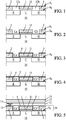
- Figures 1 to 5 are cross-sectional views of an integrated electronic circuit being manufactured, using a method according to the invention.
- an integrated electronic circuit being manufactured comprises a substrate 10 with at least one transistor formed at a surface S 0 thereof.
- the transistor when of field-effect type, comprises a source zone S and a drain zone D within the substrate 10 below the surface S 0 , separated by a channel zone C.
- a gate electrode structure has been already produced on the substrate surface S 0 above the channel zone C, which comprises a gate dielectric film 11 and a gate electrode 1.
- a source contact structure 2 and a drain contact structure 3 have been produced also on the substrate surface S 0 , above the source zone S and the drain zone D respectively.
- the gate electrode 1, the source contact structure 2 and the drain contact structure 3 are further surrounded by dielectric portions 12a and 12b, which may comprise a gate spacer around the gate electrode 1 and additional dielectric portions in circuit areas apart from the transistor.
- dielectric portions 12a and 12b may comprise a gate spacer around the gate electrode 1 and additional dielectric portions in circuit areas apart from the transistor.
- reference sign 12a denotes a portion of the gate spacer which is intermediate between the gate electrode 1 and the source contact structure 2
- reference sign 12b denotes a portion of the same gate spacer which is intermediate between the gate electrode 1 and the drain contact structure 3.
- CMP chemical-mechanical polishing step
- the upper surface S 1 has been called level plane in the general part of the description, and the upper surfaces of the gate electrode structure, and those of the source contact structure 2 and drain contact structure 3 within this level plane S 1 have been called surface portions. They are exposed until they become covered as described further below, and form interface portions after they have been covered.
- the circuit comprises a large number of such transistors distributed at the surface S 0 of the substrate 10, all processed in parallel during common processing steps.
- the substrate 10 belongs to a wafer at this stage of the circuit manufacturing process, the wafer being intended to be cut at the end of the process for producing separated circuits.
- the wafer forms the respective substrates 10 of a large number of integrated circuits all being manufactured in parallel during common processing steps.
- the circuit being manufactured is then processed by an etching step for removing at least part of the dielectric portions 12a and 12b.
- Any etching process known in the art but appropriate to the material(s) of these portions 12a and 12b may be implemented to this end, for example of wet etching type.
- a cavity Ca is produced at the location of the dielectric portion 12a, and a cavity Cb at the location of the dielectric portion 12b, as represented in figure 2 .
- the etching process may be stopped before the surface S 0 becomes uncovered at the bottom of the cavities Ca and Cb, leading to thin dielectric films possibly remaining between the substrate surface S 0 and the bottom surfaces of the cavities Ca and Cb.
- a conformal layer 4 of boron nitride (BN) is deposited on the circuit being manufactured, as represented in figure 3 .
- a conformal layer is a continuous layer with a substantially uniform and well-defined thickness, the layer following the topography of the underlying structure.
- the conformal layer 4 in the cavities Ca and Cb is only present with a uniform thickness on the surface and the sidewalls of these cavities, leaving a further opening in each cavity.
- the conformal layer 4 does not completely fill the cavities, thereby only reducing their depth.
- the cavities Ca and Cb thus altered are denoted Ca' and Cb' in figures 3-5 .
- a BN atomic layer deposition process may be implemented for providing good control of the thickness of the BN material being deposited, and also control of the quality of the material deposited.
- Deposition parameters may be implemented for obtaining BN material with diamond-like crystal structure.
- the thickness of the conformal BN layer 4 may be about 2 nm (nanometer) or less, for example.
- a chemical vapor deposition process or a radiofrequency-assisted magnetron sputtering process may be used alternatively for producing the conformal BN layer 4. All these deposition processes are well-known in the art, so that it is not necessary to describe them again here. One can refer for descriptions of such processes to any relevant publication widely available.
- a nanosheet 5 of boron nitride is applied on the circuit being manufactured, as represented in figure 4 .
- a nanosheet is a two-dimensional structure with thickness in a scale ranging from 1 to 100 nm (nanometer).
- the nanosheet 5 is applied so that it remains substantially flat, and contacts the conformal layer 4 above the gate electrode 1, the source contact structure 2 and the drain contact structure 3.
- the nanosheet 5 bridges between the gate electrode 1 and the source contact structure 2 on the one hand, and also between the gate electrode 1 and the drain contact structure 3 on the other hand. So the nanosheet 5 closes the cavities Ca' and Cb' on a side thereof which is opposite the substrate 10.
- the cavities Ca' and Cb' thus become airgaps within the first interconnect level.
- Any transfer process may be implemented for applying the nanosheet 5 on the circuit, including those processes which use a temporary support for the nanosheet 5.
- an annealing step may then be applied to the circuit, in particular for increasing adhesion between the conformal BN layer 4 and the BN nanosheet 5 at the locations where they contact each other, i.e. outside the airgaps.
- the BN conformal layer 4 may have been removed from the upper surfaces of the gate electrode 1 and the source and drain contact structures 2, 3 before the BN nanosheet 5 is applied.
- the BN nanosheet 5 is applied directly on the exposed upper surfaces of the gate electrode 1 and the source and drain contact structures 2, 3.
- the gate electrode structure, the source and drain contact structures 2, 3, the conformal BN layer 4, the airgaps Ca', Cb' and the BN nanosheet 5 form the first interconnect level 20 of the circuit (see figure 5 ).
- the conformal layer 4 and the nanosheet 5 do not create unwanted electrical path between the gate electrode 1 and the source or drain contact structure 2, 3.
- the electrical design of the circuit can thus remain unchanged with respect to one developed initially for a manufacturing process as existing before the invention.
- airgaps are created across the wafer according to the invention with uniform thickness and controlled in-plane dimensions, while allowing arranging additional interconnect levels above the BN nanosheet 5.
- the airgaps reduce interconnect capacitance values that exist between electrically conducting elements of the circuit, in particular between the gate electrode 1 and the source and drain contact structures 2 and 3.
- the conformal layer 4 is efficient for preventing electro-migration to occur or to be sufficient for causing dysfunction of the circuit, for the materials of the gate electrode 1 and source and drain contact structures 2 and 3.
- boron nitride has high heat-conductivity, it is efficient in participating to dissipate heat that is generated in the circuit when in operation. In this way, temperature increase is limited, which further participates to limiting electro-migration.
- Figure 5 shows the circuit after its manufacturing has been continued.
- Reference numbers 21, 22, 23... denote further interconnect levels which have been stacked on the BN nanosheet 5. Details of conducting parts within these interconnect levels 21, 22, 23... are not shown, except a via 12 and a track 13 within the interconnect level 21. These are for showing compatibility of the invention method with the known processes used for connecting electrically the gate electrode 1 and the source and drain contact structures 2, 3. No additional photo-lithography step is necessary, since the conformal BN layer 4 and the BN nanosheet 5 can be etched at the same time as the dielectric material of the interconnect level 21.
- the invention may be implemented while changing or adapting secondary aspects thereof, with respect to the detailed description provided before.
- it may be implemented in interconnect levels other that the first one which contains the gate electrode structures above the substrate surface.
- the invention may be combined advantageously with transistor configurations other than those located at the substrate surface as mentioned with reference to the figures.
- it can be combined with three-dimensional integration such as monolithic three-dimension integrated circuit, three-dimension stacked circuits, etc.
Landscapes
- Internal Circuitry In Semiconductor Integrated Circuit Devices (AREA)
- Insulated Gate Type Field-Effect Transistor (AREA)
- Chemical & Material Sciences (AREA)
- Inorganic Chemistry (AREA)
Abstract
Description
- The invention relates to forming airgaps within an integrated electronic circuit.
- Interconnect layers within an integrated electronic circuit each comprise electrically conducting portions such as tracks, vias and/or contact structures which are at a same level above the surface of a substrate of the circuit, and separated from each other by electrically insulating portions. One particular interconnect layer is that which is located just above the substrate surface, and which contains the gate electrode structures of the circuit field-effect transistors, and also contains their source and drain contact structures. This particular interconnect layer is commonly called first interconnect layer and its material is called interlayer dielectric material.
- Well-known issues for the interconnect layers are electro-migration of the material forming the conducting portions, mechanical strength, heat dissipation and capacitive interactions existing between neighbouring conducting portions. Electro-migration causes alterations in the shape of the conducting portions and may even produce unwanted short circuits, thereby damaging the circuit permanently. In addition, temperature increase, in particular due to insufficient heat dissipation capability during operation of the circuit, activates electro-migration. Capacitive interactions may cause additional power consumption and may reduce the operation performance of the circuit.
- Document
US 9,793,193 B1 - Document
US 9,000,594 B2 - Document
US 2017/0287811 A1 discloses implementing a heat dissipation layer over an active area of an integrated electronic circuit where at least one field-effect transistor is located. The heat dissipation layer is comprised of a single-layer or multi-layer boron nitride film, or a boron nitride nanosheet. It is formed on the circuit by a transfer process. Boron nitride provides high heat-conduction while being electrically insulating. - Starting from this situation, one object of the present invention consists in providing an efficient combination between reducing electro-migration in interconnect layers, increasing heat dissipation, and implementing airgaps while maintaining sufficient mechanical strength for the circuit.
- Another object of the invention consists in implementing such combination in a manner that is compatible with the circuit manufacturing process and tools as used before the invention.
- For meeting at least one of these objects or others, a first aspect of the present invention proposes a method for forming at least one airgap within an integrated electronic circuit, which method comprises the following steps:
- /1/ providing an integrated circuit part intended for forming part of the circuit, the circuit part exhibiting at least two exposed surface portions which coincide with one and same level plane of the circuit and are apart from each other, and the circuit part further exhibiting an open cavity located between the surface portions;
- /2/ depositing a conformal layer of boron nitride on the circuit part, so that this conformal layer covers a bottom and sidewalls of the cavity without filling this cavity up to the level plane;
- /3/ applying a boron nitride nanosheet on the circuit part so that this nanosheet is supported by the surface portions and bridges between these surface portions above the cavity, thereby forming the airgap between the conformal layer and the nanosheet; and
- /4/ optionally after step /3/, forming a further part of the circuit on the nanosheet, on a side thereof which is opposed to the cavities, so as to complete the circuit.
- Thanks to the mechanical properties of boron nitride material, the nanosheet participates to the mechanical strength of the circuit. Indeed, mechanical strength of boron nitride is more than 104 times higher than that of silica.
- Thanks to the high heat-conductivity of boron nitride material, the conformal layer and the nanosheet participate to heat dissipation during an operation of the circuit. Indeed, the thermal conductivity of boron nitride is about 180 times higher than that of silica. In this way, a temperature increase of the circuit is limited so that electro-migration is reduced.
- Additionally, capacitive interactions which may occur between conducting parts of the circuit are reduced thanks to the airgaps produced by the invention method.
- Furthermore, implementing airgaps and boron nitride according to the invention does not necessitate additional photolithography step in the circuit manufacturing process.
- Each surface portion concerned with the invention method may be formed by an electrically conducting element of the circuit, including a metal track portion or a via, a gate electrode of a transistor, a source or drain contact of a transistor, etc. Alternatively, each surface portion may be separated from an electrically conducting element of the circuit by a portion of the conformal layer on this conducting element.
- In particular, when one of the surface portions is formed by a gate electrode structure of a field-effect transistor, and another one of the surface portions is formed by a source contact structure or drain contact structure of the field-effect transistor, the airgap may be located between the gate electrode structure and the source contact structure or drain contact structure, respectively, of the field-effect transistor. In such case, the surface portions and the airgap may belong to the first interconnect layer, and the at least one airgap replaces at least part of the interlayer dielectric material of this first interconnect layer. Then, before step /1/, the circuit part may comprise a dielectric solid portion between the gate electrode structure and the source contact structure or drain contact structure, and the cavity may be formed by etching at least part of this dielectric solid portion.
- In step /2/, the conformal layer of boron nitride may be deposited using an atomic layer deposition (ALD) process or a chemical vapor deposition (CVD) process. Available existing tools for ALD or CVD may then be used, and the thickness layer can be controlled accurately in this way.
- In preferred implementations of the invention, the nanosheet may extend continuously so as to bridge above several cavities in the circuit part, each cavity being located between at least two neighboring surface portions, all of these surface portions coinciding with the same level plane of the circuit, and all the cavities being located on one and same side of the nanosheet toward a substrate of the circuit. In this way, one same nanosheet may be used for producing several airgaps in the circuit, with a single execution of step /3/. Thus the circuit manufacturing time is not increased significantly.
- Again in preferred implementations of the invention, possibly including the former ones with several airgaps per circuit part, the circuit part may be one among a plurality of circuit parts all juxtaposed within a wafer being processed for manufacturing simultaneously a plurality of integrated electronic circuits. Then, the nanosheet may be applied in step /3/ across the whole wafer so that it extends continuously on all the circuit parts of the wafer, and bridges above at least one cavity within each circuit part. In this way, one same nanosheet may be used for producing several circuits in parallel from one wafer, with a single execution of step /3/. Thus the wafer processing time is not increased significantly.
- A second aspect of the invention proposes an integrated electronic circuit with at least one airgap, which circuit comprises:
- at least two interface portions which coincide with one and same level plane within the circuit and are apart from each other;
- a nanosheet of boron nitride which extends between both interface portions;
- a cavity which is located next to the nanosheet between the interface portions, on a side of the nanosheet toward a substrate of the circuit; and
- a conformal layer of boron nitride, which covers a bottom of the cavity opposite the nanosheet, and also covers sidewalls of the cavity without filling this cavity, so that the airgap is formed by the cavity between the conformal layer and the nanosheet.
- Such circuit may be produced using a method according to the first invention aspect.
- Generally, one or several of the following additional features may be reproduced in the invention circuit:
- at least one of the interface portions may be formed by an electrically conducting element of the circuit, or may be separated from an electrically conducting element of the circuit by a portion of the conformal layer on this conducting element;
- the nanosheet may extend continuously between and next to several cavities in the circuit, each cavity being located between at least two neighboring interface portions, all of these interface portions coinciding with the same level plane of the circuit, and all the cavities being located on the same side of the nanosheet toward the substrate of the circuit;
- one of the interface portions may be formed by a gate electrode structure of a field-effect transistor, and another one of the interface portions may be formed by a source contact structure or drain contact structure of the field-effect transistor, so that the airgap is located between the gate electrode structure and the source contact structure or drain contact structure of the field-effect transistor; and
- the conformal layer of boron nitride may have diamond-like crystal structure.
-
Figures 1 to 5 are cross-sectional views of an integrated electronic circuit being manufactured, using a method according to the invention. - For clarity sake, element sizes which appear in these figures do not correspond to actual dimensions or dimension ratios. Also, same reference signs which are indicated in different ones of these figures denote identical elements of elements with identical function.
- With reference to
figure 1 , an integrated electronic circuit being manufactured comprises asubstrate 10 with at least one transistor formed at a surface S0 thereof. In a known manner, the transistor, when of field-effect type, comprises a source zone S and a drain zone D within thesubstrate 10 below the surface S0, separated by a channel zone C. A gate electrode structure has been already produced on the substrate surface S0 above the channel zone C, which comprises agate dielectric film 11 and agate electrode 1. Asource contact structure 2 and adrain contact structure 3 have been produced also on the substrate surface S0, above the source zone S and the drain zone D respectively. Thegate electrode 1, thesource contact structure 2 and thedrain contact structure 3 are further surrounded bydielectric portions gate electrode 1 and additional dielectric portions in circuit areas apart from the transistor. For example,reference sign 12a denotes a portion of the gate spacer which is intermediate between thegate electrode 1 and thesource contact structure 2, andreference sign 12b denotes a portion of the same gate spacer which is intermediate between thegate electrode 1 and thedrain contact structure 3. The circuit has been then processed by a chemical-mechanical polishing step, or CMP, for forming the upper surface S1 of the circuit parallel to the substrate surface S0. The upper surface S1 has been called level plane in the general part of the description, and the upper surfaces of the gate electrode structure, and those of thesource contact structure 2 and draincontact structure 3 within this level plane S1 have been called surface portions. They are exposed until they become covered as described further below, and form interface portions after they have been covered. - Although only one transistor has been represented in the figures, the circuit comprises a large number of such transistors distributed at the surface S0 of the
substrate 10, all processed in parallel during common processing steps. In addition, in a well-known manner, thesubstrate 10 belongs to a wafer at this stage of the circuit manufacturing process, the wafer being intended to be cut at the end of the process for producing separated circuits. Thus, the wafer forms therespective substrates 10 of a large number of integrated circuits all being manufactured in parallel during common processing steps. Although it is no longer indicated below, the circuit manufacturing steps described thereafter apply simultaneously to the whole useful area of the wafer. - The circuit being manufactured is then processed by an etching step for removing at least part of the
dielectric portions portions dielectric portion 12a, and a cavity Cb at the location of thedielectric portion 12b, as represented infigure 2 . Although not shown in thefigures 2-5 , the etching process may be stopped before the surface S0 becomes uncovered at the bottom of the cavities Ca and Cb, leading to thin dielectric films possibly remaining between the substrate surface S0 and the bottom surfaces of the cavities Ca and Cb. - Then according to the invention, a
conformal layer 4 of boron nitride (BN) is deposited on the circuit being manufactured, as represented infigure 3 . A conformal layer is a continuous layer with a substantially uniform and well-defined thickness, the layer following the topography of the underlying structure. After the deposition of theconformal layer 4, theconformal layer 4 in the cavities Ca and Cb is only present with a uniform thickness on the surface and the sidewalls of these cavities, leaving a further opening in each cavity. Theconformal layer 4 does not completely fill the cavities, thereby only reducing their depth. The cavities Ca and Cb thus altered are denoted Ca' and Cb' infigures 3-5 . A BN atomic layer deposition process may be implemented for providing good control of the thickness of the BN material being deposited, and also control of the quality of the material deposited. Deposition parameters may be implemented for obtaining BN material with diamond-like crystal structure. The thickness of theconformal BN layer 4 may be about 2 nm (nanometer) or less, for example. Possibly, a chemical vapor deposition process or a radiofrequency-assisted magnetron sputtering process may be used alternatively for producing theconformal BN layer 4. All these deposition processes are well-known in the art, so that it is not necessary to describe them again here. One can refer for descriptions of such processes to any relevant publication widely available. - In a next step of a method according to the invention, a
nanosheet 5 of boron nitride is applied on the circuit being manufactured, as represented infigure 4 . In a well-known manner, a nanosheet is a two-dimensional structure with thickness in a scale ranging from 1 to 100 nm (nanometer). Thenanosheet 5 is applied so that it remains substantially flat, and contacts theconformal layer 4 above thegate electrode 1, thesource contact structure 2 and thedrain contact structure 3. Thus, thenanosheet 5 bridges between thegate electrode 1 and thesource contact structure 2 on the one hand, and also between thegate electrode 1 and thedrain contact structure 3 on the other hand. So thenanosheet 5 closes the cavities Ca' and Cb' on a side thereof which is opposite thesubstrate 10. The cavities Ca' and Cb' thus become airgaps within the first interconnect level. Any transfer process may be implemented for applying thenanosheet 5 on the circuit, including those processes which use a temporary support for thenanosheet 5. One can refer again to any relevant publication widely available about such transfer processes. - Optionally, an annealing step may then be applied to the circuit, in particular for increasing adhesion between the
conformal BN layer 4 and theBN nanosheet 5 at the locations where they contact each other, i.e. outside the airgaps. Alternatively, the BNconformal layer 4 may have been removed from the upper surfaces of thegate electrode 1 and the source and draincontact structures BN nanosheet 5 is applied. In such case, theBN nanosheet 5 is applied directly on the exposed upper surfaces of thegate electrode 1 and the source and draincontact structures - The gate electrode structure, the source and drain
contact structures conformal BN layer 4, the airgaps Ca', Cb' and theBN nanosheet 5 form thefirst interconnect level 20 of the circuit (seefigure 5 ). - Because boron nitride material is electrically insulating, the
conformal layer 4 and thenanosheet 5 do not create unwanted electrical path between thegate electrode 1 and the source or draincontact structure - Because boron nitride material has very high mechanical strength, airgaps are created across the wafer according to the invention with uniform thickness and controlled in-plane dimensions, while allowing arranging additional interconnect levels above the
BN nanosheet 5. The airgaps reduce interconnect capacitance values that exist between electrically conducting elements of the circuit, in particular between thegate electrode 1 and the source and draincontact structures - Because boron nitride material has good barrier properties, the
conformal layer 4 is efficient for preventing electro-migration to occur or to be sufficient for causing dysfunction of the circuit, for the materials of thegate electrode 1 and source and draincontact structures - And finally, because boron nitride has high heat-conductivity, it is efficient in participating to dissipate heat that is generated in the circuit when in operation. In this way, temperature increase is limited, which further participates to limiting electro-migration.
-
Figure 5 shows the circuit after its manufacturing has been continued.Reference numbers BN nanosheet 5. Details of conducting parts within theseinterconnect levels track 13 within theinterconnect level 21. These are for showing compatibility of the invention method with the known processes used for connecting electrically thegate electrode 1 and the source and draincontact structures conformal BN layer 4 and theBN nanosheet 5 can be etched at the same time as the dielectric material of theinterconnect level 21. - It should be understood that the invention may be implemented while changing or adapting secondary aspects thereof, with respect to the detailed description provided before. In particular, it may be implemented in interconnect levels other that the first one which contains the gate electrode structures above the substrate surface.
- Also, the invention may be combined advantageously with transistor configurations other than those located at the substrate surface as mentioned with reference to the figures. In particular, it can be combined with three-dimensional integration such as monolithic three-dimension integrated circuit, three-dimension stacked circuits, etc.
Claims (13)
- A method for forming at least one airgap within an integrated electronic circuit, comprising the following steps:/1/ providing an integrated circuit part intended for forming part of the circuit, said circuit part exhibiting at least two exposed surface portions which coincide with one and same level plane (S1) of the circuit and are apart from each other, and said circuit part further exhibiting an open cavity (Ca, Cb) located between the surface portions;/2/ depositing a conformal layer (4) of boron nitride on the circuit part, so that said conformal layer covers a bottom and sidewalls of the cavity (Ca, Cb) without filling said cavity up to the level plane (S1); and/3/ applying a boron nitride nanosheet (5) on the circuit part so that said nanosheet is supported by the surface portions and bridges between said surface portions above the cavity (Ca', Cb'), thereby forming the airgap between the conformal layer (4) and the nanosheet (5).
- The method of claim 1, wherein at least one of the surface portions is formed by an electrically conducting element of the circuit, or is separated from an electrically conducting element of the circuit by a portion of the conformal layer (4) on said conducting element.
- The method of claim 1 or 2, wherein the conformal layer (4) of boron nitride is deposited in step /2/ using an atomic layer deposition process or a chemical vapor deposition process.
- The method of any one of the preceding claims, wherein the nanosheet (5) extends continuously so as to bridge above several cavities (Ca', Cb') in the circuit part, each cavity being located between at least two neighboring surface portions, all of said surface portions coinciding with the same level plane (S1) of the circuit, and all the cavities being located on one and same side of the nanosheet toward a substrate (10) of the circuit.
- The method of claim 4, further comprising the following step executed after step /3/:/4/ forming a further part of the circuit on the nanosheet (5), on a side thereof which is opposed to the cavities (Ca', Cb'), so as to complete the circuit.
- The method of any one of the preceding claims, wherein the circuit part is one among a plurality of circuit parts all juxtaposed within a wafer being processed for manufacturing simultaneously a plurality of integrated electronic circuits, and the nanosheet (5) is applied in step /3/ across the whole wafer so that said nanosheet extends continuously on all the circuit parts of the wafer, and bridges above at least one cavity (Ca', Cb') within each circuit part.
- The method of any one of the preceding claims, wherein one of the surface portions is formed by a gate electrode structure (1) of a field-effect transistor, and another one of the surface portions is formed by a source contact structure (2) or drain contact structure (3) of the field-effect transistor, so that the airgap is located between the gate electrode structure and the source contact structure or drain contact structure, respectively, of the field-effect transistor.
- The method of claim 7, wherein the circuit part comprises before step /1/ a dielectric solid portion (12a, 12b) between the gate electrode structure (1) and the source contact structure (2) or drain contact structure (3), and the cavity (Ca, Cb) is formed by etching at least part of said dielectric solid portion.
- An integrated electronic circuit with at least one airgap, comprising:- at least two interface portions which coincide with one and same level plane (S1) within the circuit and are apart from each other;- a nanosheet (5) of boron nitride which extends between both interface portions;- a cavity (Ca', Cb') located next to the nanosheet (5) between the interface portions, on a side of said nanosheet toward a substrate (10) of the circuit; and- a conformal layer (4) of boron nitride, which covers a bottom of the cavity (Ca', Cb') opposite the nanosheet (5), and also covers sidewalls of the cavity without filling said cavity, so that the airgap is formed by the cavity between the conformal layer and the nanosheet.
- The integrated electronic circuit of claim 9, wherein at least one of the interface portions is formed by an electrically conducting element of the circuit, or is separated from an electrically conducting element of the circuit by a portion of the conformal layer (4) on said conducting element.
- The integrated electronic circuit of claim 9 or 10, wherein the nanosheet (5) extends continuously between and next to several cavities (Ca', Cb') in the circuit, each cavity being located between at least two neighboring interface portions, all of said interface portions coinciding with the same level plane (S1) of the circuit, and all the cavities being located on the same side of the nanosheet toward the substrate (10) of the circuit.
- The integrated electronic circuit of any one of the preceding claims, wherein one of the interface portions is formed by a gate electrode structure (1) of a field-effect transistor, and another one of the interface portions is formed by a source contact structure (2) or drain contact structure (3) of the field-effect transistor, so that the airgap is located between the gate electrode structure and the source contact structure or drain contact structure of the field-effect transistor.
- The integrated electronic circuit of any one of claims 9 to 12, wherein the conformal layer (4) of boron nitride has diamond-like crystal structure.
Priority Applications (2)
| Application Number | Priority Date | Filing Date | Title |
|---|---|---|---|
| EP18205965.9A EP3654372B1 (en) | 2018-11-13 | 2018-11-13 | Method of forming an integrated circuit with airgaps and corresponding integrated circuit |
| US16/577,332 US11276606B2 (en) | 2018-11-13 | 2019-09-20 | Integrated electronic circuit with airgaps |
Applications Claiming Priority (1)
| Application Number | Priority Date | Filing Date | Title |
|---|---|---|---|
| EP18205965.9A EP3654372B1 (en) | 2018-11-13 | 2018-11-13 | Method of forming an integrated circuit with airgaps and corresponding integrated circuit |
Publications (2)
| Publication Number | Publication Date |
|---|---|
| EP3654372A1 true EP3654372A1 (en) | 2020-05-20 |
| EP3654372B1 EP3654372B1 (en) | 2021-04-21 |
Family
ID=64316293
Family Applications (1)
| Application Number | Title | Priority Date | Filing Date |
|---|---|---|---|
| EP18205965.9A Active EP3654372B1 (en) | 2018-11-13 | 2018-11-13 | Method of forming an integrated circuit with airgaps and corresponding integrated circuit |
Country Status (2)
| Country | Link |
|---|---|
| US (1) | US11276606B2 (en) |
| EP (1) | EP3654372B1 (en) |
Citations (6)
| Publication number | Priority date | Publication date | Assignee | Title |
|---|---|---|---|---|
| US20040102031A1 (en) * | 2002-11-21 | 2004-05-27 | Kloster Grant M. | Low-K dielectric structure and method |
| US20140061926A1 (en) * | 2012-09-05 | 2014-03-06 | Kyu-hee Han | Semiconductor devices including supporting patterns in gap regions between conductive patterns and methods of fabricating the same |
| US9000594B2 (en) | 2012-07-18 | 2015-04-07 | International Business Machines Corporation | Use of graphene to limit copper surface oxidation, diffusion and electromigration in interconnect structures |
| EP3082161A1 (en) * | 2015-04-15 | 2016-10-19 | Freescale Semiconductor, Inc. | Method of forming inter-level dielectric structures on semiconductor devices |
| US20170287811A1 (en) | 2016-04-05 | 2017-10-05 | Gpower Semiconductor, Inc. | Semiconductor device |
| US9793193B1 (en) | 2016-09-29 | 2017-10-17 | International Business Machines Corporation | Air gap and air spacer pinch off |
Family Cites Families (10)
| Publication number | Priority date | Publication date | Assignee | Title |
|---|---|---|---|---|
| US6627168B1 (en) * | 1999-10-01 | 2003-09-30 | Showa Denko Kabushiki Kaisha | Method for growing diamond and cubic boron nitride crystals |
| US20090093100A1 (en) * | 2007-10-09 | 2009-04-09 | Li-Qun Xia | Method for forming an air gap in multilevel interconnect structure |
| US7964442B2 (en) * | 2007-10-09 | 2011-06-21 | Applied Materials, Inc. | Methods to obtain low k dielectric barrier with superior etch resistivity |
| US7928003B2 (en) | 2008-10-10 | 2011-04-19 | Applied Materials, Inc. | Air gap interconnects using carbon-based films |
| WO2013101096A1 (en) | 2011-12-29 | 2013-07-04 | Intel Corporation | Airgap interconnect with hood layer and method of forming |
| CN102956611B (en) | 2012-11-12 | 2017-03-15 | 上海集成电路研发中心有限公司 | A kind of air gap/graphene interconnection structure and preparation method thereof |
| CN104637898B (en) | 2014-12-08 | 2019-01-11 | 上海大学 | The heat-conductive composite material layer and electronic device conductive structure packaging method of integrated circuit device |
| US9865738B2 (en) * | 2016-04-29 | 2018-01-09 | Samsung Electronics Co., Ltd. | Fin field effect transistor (FinFET) having air gap and method of fabricating the same |
| US10043753B2 (en) | 2016-12-13 | 2018-08-07 | Globalfoundries Inc. | Airgaps to isolate metallization features |
| US10854506B2 (en) * | 2018-09-27 | 2020-12-01 | Taiwan Semiconductor Manufacturing Co., Ltd. | Semiconductor device and manufacturing method thereof |
-
2018
- 2018-11-13 EP EP18205965.9A patent/EP3654372B1/en active Active
-
2019
- 2019-09-20 US US16/577,332 patent/US11276606B2/en active Active
Patent Citations (6)
| Publication number | Priority date | Publication date | Assignee | Title |
|---|---|---|---|---|
| US20040102031A1 (en) * | 2002-11-21 | 2004-05-27 | Kloster Grant M. | Low-K dielectric structure and method |
| US9000594B2 (en) | 2012-07-18 | 2015-04-07 | International Business Machines Corporation | Use of graphene to limit copper surface oxidation, diffusion and electromigration in interconnect structures |
| US20140061926A1 (en) * | 2012-09-05 | 2014-03-06 | Kyu-hee Han | Semiconductor devices including supporting patterns in gap regions between conductive patterns and methods of fabricating the same |
| EP3082161A1 (en) * | 2015-04-15 | 2016-10-19 | Freescale Semiconductor, Inc. | Method of forming inter-level dielectric structures on semiconductor devices |
| US20170287811A1 (en) | 2016-04-05 | 2017-10-05 | Gpower Semiconductor, Inc. | Semiconductor device |
| US9793193B1 (en) | 2016-09-29 | 2017-10-17 | International Business Machines Corporation | Air gap and air spacer pinch off |
Also Published As
| Publication number | Publication date |
|---|---|
| EP3654372B1 (en) | 2021-04-21 |
| US11276606B2 (en) | 2022-03-15 |
| US20200152503A1 (en) | 2020-05-14 |
Similar Documents
| Publication | Publication Date | Title |
|---|---|---|
| US20220181198A1 (en) | Self aligned buried power rail | |
| JP3790469B2 (en) | Semiconductor device | |
| TWI466293B (en) | Integrated circuit with metal gate stack and forming method thereof | |
| CN103094275B (en) | There is integrated circuit and the manufacture method thereof of MOM capacitor | |
| US10361079B2 (en) | Multi-angled deposition and masking for custom spacer trim and selected spacer removal | |
| JP4339946B2 (en) | Manufacturing method of semiconductor device | |
| KR102818476B1 (en) | Fully aligned subtractive processes and electronic devices therefrom | |
| JP7447152B2 (en) | Three-dimensional memory device with source contacts connected by an adhesive layer and method for forming the same | |
| JP2004193563A (en) | Semiconductor device having MIM capacitor | |
| US20070144628A1 (en) | Intermediate anneal for metal deposition | |
| EP3312882B1 (en) | A method of patterning a target layer | |
| CN108807531B (en) | Semiconductor device and method for manufacturing the same | |
| KR100237096B1 (en) | Method of manufacturing a semiconductor device | |
| CN110858562A (en) | Semiconductor element manufacturing method and semiconductor element manufactured by same | |
| CN114446928B (en) | MIM capacitor structure | |
| US11646223B2 (en) | Metal lead, semiconductor device and methods of fabricating the same | |
| CN102237295B (en) | Semiconductor Structure Fabrication Method | |
| EP3146565A1 (en) | Shunt of p-gate to n-gate boundary resistance for metal gate technologies | |
| EP3654372B1 (en) | Method of forming an integrated circuit with airgaps and corresponding integrated circuit | |
| US20250126884A1 (en) | Forksheet transistor structure | |
| TWI851236B (en) | Reduced capacitance between power via bar and gates | |
| US20030064553A1 (en) | Method of producing semiconductor device and its structure | |
| TW202042317A (en) | Method of manufacturing semiconductor device | |
| KR20070098319A (en) | Semiconductor device having a spacer of nitride film-oxide film-nitride film structure and method of manufacturing same | |
| CN110473829B (en) | Interlayer film manufacturing method |
Legal Events
| Date | Code | Title | Description |
|---|---|---|---|
| PUAI | Public reference made under article 153(3) epc to a published international application that has entered the european phase |
Free format text: ORIGINAL CODE: 0009012 |
|
| STAA | Information on the status of an ep patent application or granted ep patent |
Free format text: STATUS: THE APPLICATION HAS BEEN PUBLISHED |
|
| AK | Designated contracting states |
Kind code of ref document: A1 Designated state(s): AL AT BE BG CH CY CZ DE DK EE ES FI FR GB GR HR HU IE IS IT LI LT LU LV MC MK MT NL NO PL PT RO RS SE SI SK SM TR |
|
| AX | Request for extension of the european patent |
Extension state: BA ME |
|
| STAA | Information on the status of an ep patent application or granted ep patent |
Free format text: STATUS: REQUEST FOR EXAMINATION WAS MADE |
|
| 17P | Request for examination filed |
Effective date: 20201012 |
|
| RBV | Designated contracting states (corrected) |
Designated state(s): AL AT BE BG CH CY CZ DE DK EE ES FI FR GB GR HR HU IE IS IT LI LT LU LV MC MK MT NL NO PL PT RO RS SE SI SK SM TR |
|
| GRAP | Despatch of communication of intention to grant a patent |
Free format text: ORIGINAL CODE: EPIDOSNIGR1 |
|
| STAA | Information on the status of an ep patent application or granted ep patent |
Free format text: STATUS: GRANT OF PATENT IS INTENDED |
|
| INTG | Intention to grant announced |
Effective date: 20201210 |
|
| GRAS | Grant fee paid |
Free format text: ORIGINAL CODE: EPIDOSNIGR3 |
|
| GRAA | (expected) grant |
Free format text: ORIGINAL CODE: 0009210 |
|
| STAA | Information on the status of an ep patent application or granted ep patent |
Free format text: STATUS: THE PATENT HAS BEEN GRANTED |
|
| AK | Designated contracting states |
Kind code of ref document: B1 Designated state(s): AL AT BE BG CH CY CZ DE DK EE ES FI FR GB GR HR HU IE IS IT LI LT LU LV MC MK MT NL NO PL PT RO RS SE SI SK SM TR |
|
| REG | Reference to a national code |
Ref country code: GB Ref legal event code: FG4D |
|
| REG | Reference to a national code |
Ref country code: CH Ref legal event code: EP |
|
| REG | Reference to a national code |
Ref country code: DE Ref legal event code: R096 Ref document number: 602018015789 Country of ref document: DE Ref country code: IE Ref legal event code: FG4D |
|
| REG | Reference to a national code |
Ref country code: AT Ref legal event code: REF Ref document number: 1385537 Country of ref document: AT Kind code of ref document: T Effective date: 20210515 |
|
| REG | Reference to a national code |
Ref country code: LT Ref legal event code: MG9D |
|
| REG | Reference to a national code |
Ref country code: AT Ref legal event code: MK05 Ref document number: 1385537 Country of ref document: AT Kind code of ref document: T Effective date: 20210421 |
|
| REG | Reference to a national code |
Ref country code: NL Ref legal event code: MP Effective date: 20210421 |
|
| PG25 | Lapsed in a contracting state [announced via postgrant information from national office to epo] |
Ref country code: NL Free format text: LAPSE BECAUSE OF FAILURE TO SUBMIT A TRANSLATION OF THE DESCRIPTION OR TO PAY THE FEE WITHIN THE PRESCRIBED TIME-LIMIT Effective date: 20210421 Ref country code: BG Free format text: LAPSE BECAUSE OF FAILURE TO SUBMIT A TRANSLATION OF THE DESCRIPTION OR TO PAY THE FEE WITHIN THE PRESCRIBED TIME-LIMIT Effective date: 20210721 Ref country code: AT Free format text: LAPSE BECAUSE OF FAILURE TO SUBMIT A TRANSLATION OF THE DESCRIPTION OR TO PAY THE FEE WITHIN THE PRESCRIBED TIME-LIMIT Effective date: 20210421 Ref country code: FI Free format text: LAPSE BECAUSE OF FAILURE TO SUBMIT A TRANSLATION OF THE DESCRIPTION OR TO PAY THE FEE WITHIN THE PRESCRIBED TIME-LIMIT Effective date: 20210421 Ref country code: LT Free format text: LAPSE BECAUSE OF FAILURE TO SUBMIT A TRANSLATION OF THE DESCRIPTION OR TO PAY THE FEE WITHIN THE PRESCRIBED TIME-LIMIT Effective date: 20210421 Ref country code: HR Free format text: LAPSE BECAUSE OF FAILURE TO SUBMIT A TRANSLATION OF THE DESCRIPTION OR TO PAY THE FEE WITHIN THE PRESCRIBED TIME-LIMIT Effective date: 20210421 |
|
| PG25 | Lapsed in a contracting state [announced via postgrant information from national office to epo] |
Ref country code: RS Free format text: LAPSE BECAUSE OF FAILURE TO SUBMIT A TRANSLATION OF THE DESCRIPTION OR TO PAY THE FEE WITHIN THE PRESCRIBED TIME-LIMIT Effective date: 20210421 Ref country code: SE Free format text: LAPSE BECAUSE OF FAILURE TO SUBMIT A TRANSLATION OF THE DESCRIPTION OR TO PAY THE FEE WITHIN THE PRESCRIBED TIME-LIMIT Effective date: 20210421 Ref country code: PL Free format text: LAPSE BECAUSE OF FAILURE TO SUBMIT A TRANSLATION OF THE DESCRIPTION OR TO PAY THE FEE WITHIN THE PRESCRIBED TIME-LIMIT Effective date: 20210421 Ref country code: NO Free format text: LAPSE BECAUSE OF FAILURE TO SUBMIT A TRANSLATION OF THE DESCRIPTION OR TO PAY THE FEE WITHIN THE PRESCRIBED TIME-LIMIT Effective date: 20210721 Ref country code: LV Free format text: LAPSE BECAUSE OF FAILURE TO SUBMIT A TRANSLATION OF THE DESCRIPTION OR TO PAY THE FEE WITHIN THE PRESCRIBED TIME-LIMIT Effective date: 20210421 Ref country code: PT Free format text: LAPSE BECAUSE OF FAILURE TO SUBMIT A TRANSLATION OF THE DESCRIPTION OR TO PAY THE FEE WITHIN THE PRESCRIBED TIME-LIMIT Effective date: 20210823 Ref country code: GR Free format text: LAPSE BECAUSE OF FAILURE TO SUBMIT A TRANSLATION OF THE DESCRIPTION OR TO PAY THE FEE WITHIN THE PRESCRIBED TIME-LIMIT Effective date: 20210722 Ref country code: IS Free format text: LAPSE BECAUSE OF FAILURE TO SUBMIT A TRANSLATION OF THE DESCRIPTION OR TO PAY THE FEE WITHIN THE PRESCRIBED TIME-LIMIT Effective date: 20210821 |
|
| REG | Reference to a national code |
Ref country code: DE Ref legal event code: R097 Ref document number: 602018015789 Country of ref document: DE |
|
| PG25 | Lapsed in a contracting state [announced via postgrant information from national office to epo] |
Ref country code: ES Free format text: LAPSE BECAUSE OF FAILURE TO SUBMIT A TRANSLATION OF THE DESCRIPTION OR TO PAY THE FEE WITHIN THE PRESCRIBED TIME-LIMIT Effective date: 20210421 Ref country code: EE Free format text: LAPSE BECAUSE OF FAILURE TO SUBMIT A TRANSLATION OF THE DESCRIPTION OR TO PAY THE FEE WITHIN THE PRESCRIBED TIME-LIMIT Effective date: 20210421 Ref country code: SM Free format text: LAPSE BECAUSE OF FAILURE TO SUBMIT A TRANSLATION OF THE DESCRIPTION OR TO PAY THE FEE WITHIN THE PRESCRIBED TIME-LIMIT Effective date: 20210421 Ref country code: SK Free format text: LAPSE BECAUSE OF FAILURE TO SUBMIT A TRANSLATION OF THE DESCRIPTION OR TO PAY THE FEE WITHIN THE PRESCRIBED TIME-LIMIT Effective date: 20210421 Ref country code: DK Free format text: LAPSE BECAUSE OF FAILURE TO SUBMIT A TRANSLATION OF THE DESCRIPTION OR TO PAY THE FEE WITHIN THE PRESCRIBED TIME-LIMIT Effective date: 20210421 Ref country code: CZ Free format text: LAPSE BECAUSE OF FAILURE TO SUBMIT A TRANSLATION OF THE DESCRIPTION OR TO PAY THE FEE WITHIN THE PRESCRIBED TIME-LIMIT Effective date: 20210421 Ref country code: RO Free format text: LAPSE BECAUSE OF FAILURE TO SUBMIT A TRANSLATION OF THE DESCRIPTION OR TO PAY THE FEE WITHIN THE PRESCRIBED TIME-LIMIT Effective date: 20210421 |
|
| PLBE | No opposition filed within time limit |
Free format text: ORIGINAL CODE: 0009261 |
|
| STAA | Information on the status of an ep patent application or granted ep patent |
Free format text: STATUS: NO OPPOSITION FILED WITHIN TIME LIMIT |
|
| 26N | No opposition filed |
Effective date: 20220124 |
|
| PG25 | Lapsed in a contracting state [announced via postgrant information from national office to epo] |
Ref country code: IS Free format text: LAPSE BECAUSE OF FAILURE TO SUBMIT A TRANSLATION OF THE DESCRIPTION OR TO PAY THE FEE WITHIN THE PRESCRIBED TIME-LIMIT Effective date: 20210821 Ref country code: AL Free format text: LAPSE BECAUSE OF FAILURE TO SUBMIT A TRANSLATION OF THE DESCRIPTION OR TO PAY THE FEE WITHIN THE PRESCRIBED TIME-LIMIT Effective date: 20210421 |
|
| PG25 | Lapsed in a contracting state [announced via postgrant information from national office to epo] |
Ref country code: MC Free format text: LAPSE BECAUSE OF FAILURE TO SUBMIT A TRANSLATION OF THE DESCRIPTION OR TO PAY THE FEE WITHIN THE PRESCRIBED TIME-LIMIT Effective date: 20210421 |
|
| REG | Reference to a national code |
Ref country code: CH Ref legal event code: PL |
|
| PG25 | Lapsed in a contracting state [announced via postgrant information from national office to epo] |
Ref country code: LU Free format text: LAPSE BECAUSE OF NON-PAYMENT OF DUE FEES Effective date: 20211113 Ref country code: IT Free format text: LAPSE BECAUSE OF FAILURE TO SUBMIT A TRANSLATION OF THE DESCRIPTION OR TO PAY THE FEE WITHIN THE PRESCRIBED TIME-LIMIT Effective date: 20210421 Ref country code: BE Free format text: LAPSE BECAUSE OF NON-PAYMENT OF DUE FEES Effective date: 20211130 |
|
| REG | Reference to a national code |
Ref country code: BE Ref legal event code: MM Effective date: 20211130 |
|
| PG25 | Lapsed in a contracting state [announced via postgrant information from national office to epo] |
Ref country code: LI Free format text: LAPSE BECAUSE OF NON-PAYMENT OF DUE FEES Effective date: 20211130 Ref country code: CH Free format text: LAPSE BECAUSE OF NON-PAYMENT OF DUE FEES Effective date: 20211130 |
|
| PG25 | Lapsed in a contracting state [announced via postgrant information from national office to epo] |
Ref country code: IE Free format text: LAPSE BECAUSE OF NON-PAYMENT OF DUE FEES Effective date: 20211113 |
|
| PG25 | Lapsed in a contracting state [announced via postgrant information from national office to epo] |
Ref country code: FR Free format text: LAPSE BECAUSE OF NON-PAYMENT OF DUE FEES Effective date: 20211130 |
|
| P01 | Opt-out of the competence of the unified patent court (upc) registered |
Effective date: 20230513 |
|
| PG25 | Lapsed in a contracting state [announced via postgrant information from national office to epo] |
Ref country code: CY Free format text: LAPSE BECAUSE OF FAILURE TO SUBMIT A TRANSLATION OF THE DESCRIPTION OR TO PAY THE FEE WITHIN THE PRESCRIBED TIME-LIMIT Effective date: 20210421 |
|
| GBPC | Gb: european patent ceased through non-payment of renewal fee |
Effective date: 20221113 |
|
| PG25 | Lapsed in a contracting state [announced via postgrant information from national office to epo] |
Ref country code: HU Free format text: LAPSE BECAUSE OF FAILURE TO SUBMIT A TRANSLATION OF THE DESCRIPTION OR TO PAY THE FEE WITHIN THE PRESCRIBED TIME-LIMIT; INVALID AB INITIO Effective date: 20181113 |
|
| PG25 | Lapsed in a contracting state [announced via postgrant information from national office to epo] |
Ref country code: GB Free format text: LAPSE BECAUSE OF NON-PAYMENT OF DUE FEES Effective date: 20221113 |
|
| PG25 | Lapsed in a contracting state [announced via postgrant information from national office to epo] |
Ref country code: MK Free format text: LAPSE BECAUSE OF FAILURE TO SUBMIT A TRANSLATION OF THE DESCRIPTION OR TO PAY THE FEE WITHIN THE PRESCRIBED TIME-LIMIT Effective date: 20210421 |
|
| PG25 | Lapsed in a contracting state [announced via postgrant information from national office to epo] |
Ref country code: TR Free format text: LAPSE BECAUSE OF FAILURE TO SUBMIT A TRANSLATION OF THE DESCRIPTION OR TO PAY THE FEE WITHIN THE PRESCRIBED TIME-LIMIT Effective date: 20210421 |
|
| PG25 | Lapsed in a contracting state [announced via postgrant information from national office to epo] |
Ref country code: MT Free format text: LAPSE BECAUSE OF FAILURE TO SUBMIT A TRANSLATION OF THE DESCRIPTION OR TO PAY THE FEE WITHIN THE PRESCRIBED TIME-LIMIT Effective date: 20210421 |
|
| REG | Reference to a national code |
Ref country code: DE Ref legal event code: R079 Ref document number: 602018015789 Country of ref document: DE Free format text: PREVIOUS MAIN CLASS: H01L0023522000 Ipc: H10W0020400000 |
|
| PGFP | Annual fee paid to national office [announced via postgrant information from national office to epo] |
Ref country code: DE Payment date: 20251022 Year of fee payment: 8 |