EP3654134A1 - Information processing apparatus capable of detecting software tampering and control method therefor - Google Patents
Information processing apparatus capable of detecting software tampering and control method therefor Download PDFInfo
- Publication number
- EP3654134A1 EP3654134A1 EP19207691.7A EP19207691A EP3654134A1 EP 3654134 A1 EP3654134 A1 EP 3654134A1 EP 19207691 A EP19207691 A EP 19207691A EP 3654134 A1 EP3654134 A1 EP 3654134A1
- Authority
- EP
- European Patent Office
- Prior art keywords
- clock signal
- frequency
- verification
- processing apparatus
- information processing
- Prior art date
- Legal status (The legal status is an assumption and is not a legal conclusion. Google has not performed a legal analysis and makes no representation as to the accuracy of the status listed.)
- Granted
Links
Images




Classifications
-
- G—PHYSICS
- G06—COMPUTING OR CALCULATING; COUNTING
- G06F—ELECTRIC DIGITAL DATA PROCESSING
- G06F1/00—Details not covered by groups G06F3/00 - G06F13/00 and G06F21/00
- G06F1/04—Generating or distributing clock signals or signals derived directly therefrom
- G06F1/06—Clock generators producing several clock signals
-
- G—PHYSICS
- G06—COMPUTING OR CALCULATING; COUNTING
- G06F—ELECTRIC DIGITAL DATA PROCESSING
- G06F21/00—Security arrangements for protecting computers, components thereof, programs or data against unauthorised activity
- G06F21/50—Monitoring users, programs or devices to maintain the integrity of platforms, e.g. of processors, firmware or operating systems
- G06F21/55—Detecting local intrusion or implementing counter-measures
- G06F21/56—Computer malware detection or handling, e.g. anti-virus arrangements
- G06F21/566—Dynamic detection, i.e. detection performed at run-time, e.g. emulation, suspicious activities
-
- G—PHYSICS
- G06—COMPUTING OR CALCULATING; COUNTING
- G06F—ELECTRIC DIGITAL DATA PROCESSING
- G06F1/00—Details not covered by groups G06F3/00 - G06F13/00 and G06F21/00
- G06F1/04—Generating or distributing clock signals or signals derived directly therefrom
- G06F1/08—Clock generators with changeable or programmable clock frequency
-
- G—PHYSICS
- G06—COMPUTING OR CALCULATING; COUNTING
- G06F—ELECTRIC DIGITAL DATA PROCESSING
- G06F1/00—Details not covered by groups G06F3/00 - G06F13/00 and G06F21/00
- G06F1/04—Generating or distributing clock signals or signals derived directly therefrom
- G06F1/12—Synchronisation of different clock signals provided by a plurality of clock generators
-
- G—PHYSICS
- G06—COMPUTING OR CALCULATING; COUNTING
- G06F—ELECTRIC DIGITAL DATA PROCESSING
- G06F21/00—Security arrangements for protecting computers, components thereof, programs or data against unauthorised activity
- G06F21/50—Monitoring users, programs or devices to maintain the integrity of platforms, e.g. of processors, firmware or operating systems
- G06F21/51—Monitoring users, programs or devices to maintain the integrity of platforms, e.g. of processors, firmware or operating systems at application loading time, e.g. accepting, rejecting, starting or inhibiting executable software based on integrity or source reliability
-
- G—PHYSICS
- G06—COMPUTING OR CALCULATING; COUNTING
- G06F—ELECTRIC DIGITAL DATA PROCESSING
- G06F21/00—Security arrangements for protecting computers, components thereof, programs or data against unauthorised activity
- G06F21/50—Monitoring users, programs or devices to maintain the integrity of platforms, e.g. of processors, firmware or operating systems
- G06F21/57—Certifying or maintaining trusted computer platforms, e.g. secure boots or power-downs, version controls, system software checks, secure updates or assessing vulnerabilities
-
- G—PHYSICS
- G06—COMPUTING OR CALCULATING; COUNTING
- G06F—ELECTRIC DIGITAL DATA PROCESSING
- G06F21/00—Security arrangements for protecting computers, components thereof, programs or data against unauthorised activity
- G06F21/70—Protecting specific internal or peripheral components, in which the protection of a component leads to protection of the entire computer
- G06F21/81—Protecting specific internal or peripheral components, in which the protection of a component leads to protection of the entire computer by operating on the power supply, e.g. enabling or disabling power-on, sleep or resume operations
-
- G—PHYSICS
- G06—COMPUTING OR CALCULATING; COUNTING
- G06F—ELECTRIC DIGITAL DATA PROCESSING
- G06F3/00—Input arrangements for transferring data to be processed into a form capable of being handled by the computer; Output arrangements for transferring data from processing unit to output unit, e.g. interface arrangements
- G06F3/12—Digital output to print unit, e.g. line printer, chain printer
- G06F3/1201—Dedicated interfaces to print systems
- G06F3/1202—Dedicated interfaces to print systems specifically adapted to achieve a particular effect
- G06F3/1222—Increasing security of the print job
-
- G—PHYSICS
- G06—COMPUTING OR CALCULATING; COUNTING
- G06F—ELECTRIC DIGITAL DATA PROCESSING
- G06F3/00—Input arrangements for transferring data to be processed into a form capable of being handled by the computer; Output arrangements for transferring data from processing unit to output unit, e.g. interface arrangements
- G06F3/12—Digital output to print unit, e.g. line printer, chain printer
- G06F3/1201—Dedicated interfaces to print systems
- G06F3/1223—Dedicated interfaces to print systems specifically adapted to use a particular technique
- G06F3/1237—Print job management
- G06F3/1238—Secure printing, e.g. user identification, user rights for device usage, unallowed content, blanking portions or fields of a page, releasing held jobs
-
- G—PHYSICS
- G06—COMPUTING OR CALCULATING; COUNTING
- G06F—ELECTRIC DIGITAL DATA PROCESSING
- G06F9/00—Arrangements for program control, e.g. control units
- G06F9/06—Arrangements for program control, e.g. control units using stored programs, i.e. using an internal store of processing equipment to receive or retain programs
- G06F9/44—Arrangements for executing specific programs
- G06F9/4401—Bootstrapping
-
- H—ELECTRICITY
- H04—ELECTRIC COMMUNICATION TECHNIQUE
- H04N—PICTORIAL COMMUNICATION, e.g. TELEVISION
- H04N1/00—Scanning, transmission or reproduction of documents or the like, e.g. facsimile transmission; Details thereof
- H04N1/00127—Connection or combination of a still picture apparatus with another apparatus, e.g. for storage, processing or transmission of still picture signals or of information associated with a still picture
- H04N1/00204—Connection or combination of a still picture apparatus with another apparatus, e.g. for storage, processing or transmission of still picture signals or of information associated with a still picture with a digital computer or a digital computer system, e.g. an internet server
- H04N1/00244—Connection or combination of a still picture apparatus with another apparatus, e.g. for storage, processing or transmission of still picture signals or of information associated with a still picture with a digital computer or a digital computer system, e.g. an internet server with a server, e.g. an internet server
-
- H—ELECTRICITY
- H04—ELECTRIC COMMUNICATION TECHNIQUE
- H04N—PICTORIAL COMMUNICATION, e.g. TELEVISION
- H04N1/00—Scanning, transmission or reproduction of documents or the like, e.g. facsimile transmission; Details thereof
- H04N1/00838—Preventing unauthorised reproduction
- H04N1/0088—Detecting or preventing tampering attacks on the reproduction system
-
- H—ELECTRICITY
- H04—ELECTRIC COMMUNICATION TECHNIQUE
- H04N—PICTORIAL COMMUNICATION, e.g. TELEVISION
- H04N1/00—Scanning, transmission or reproduction of documents or the like, e.g. facsimile transmission; Details thereof
- H04N1/00912—Arrangements for controlling a still picture apparatus or components thereof not otherwise provided for
- H04N1/00938—Software related arrangements, e.g. loading applications
-
- G—PHYSICS
- G06—COMPUTING OR CALCULATING; COUNTING
- G06F—ELECTRIC DIGITAL DATA PROCESSING
- G06F2221/00—Indexing scheme relating to security arrangements for protecting computers, components thereof, programs or data against unauthorised activity
- G06F2221/03—Indexing scheme relating to G06F21/50, monitoring users, programs or devices to maintain the integrity of platforms
- G06F2221/033—Test or assess software
-
- H—ELECTRICITY
- H04—ELECTRIC COMMUNICATION TECHNIQUE
- H04N—PICTORIAL COMMUNICATION, e.g. TELEVISION
- H04N2201/00—Indexing scheme relating to scanning, transmission or reproduction of documents or the like, and to details thereof
- H04N2201/0077—Types of the still picture apparatus
- H04N2201/0094—Multifunctional device, i.e. a device capable of all of reading, reproducing, copying, facsimile transception, file transception
-
- Y—GENERAL TAGGING OF NEW TECHNOLOGICAL DEVELOPMENTS; GENERAL TAGGING OF CROSS-SECTIONAL TECHNOLOGIES SPANNING OVER SEVERAL SECTIONS OF THE IPC; TECHNICAL SUBJECTS COVERED BY FORMER USPC CROSS-REFERENCE ART COLLECTIONS [XRACs] AND DIGESTS
- Y02—TECHNOLOGIES OR APPLICATIONS FOR MITIGATION OR ADAPTATION AGAINST CLIMATE CHANGE
- Y02D—CLIMATE CHANGE MITIGATION TECHNOLOGIES IN INFORMATION AND COMMUNICATION TECHNOLOGIES [ICT], I.E. INFORMATION AND COMMUNICATION TECHNOLOGIES AIMING AT THE REDUCTION OF THEIR OWN ENERGY USE
- Y02D10/00—Energy efficient computing, e.g. low power processors, power management or thermal management
Definitions
- the present invention relates to an information processing apparatus capable of detecting software tampering and the like.
- An information processing apparatus that detects software tampering (hereinafter referred to as tampering detection) and prohibits execution of software for which tampering is detected.
- tampering detection software tampering
- a sub central processing unit CPU
- main CPU main central processing unit
- main CPU executes software that has been successfully verified.
- execution of the software is prohibited.
- ASV adaptive supply voltage
- a fast device a device capable of operating at a predetermined frequency even with a voltage lower than a predetermined voltage
- an operation at the predetermined frequency is realized by applying the voltage lower than the predetermined voltage.
- a slow device a device that operates at a predetermined frequency only with a voltage higher than a predetermined voltage
- an operation at the predetermined frequency is realized by applying the voltage higher than the predetermined voltage.
- a device In a case where a device is a slow device, operation of the device may be unstable unless a voltage necessary for the device is input and then a clock signal having a predetermined frequency is input. Thus, until the voltage necessary for the device is input, a clock signal having a frequency lower than the predetermined frequency is input. After the voltage necessary for the device is input, the clock signal having the predetermined frequency is input to the device using, for example, a phase-locked loop circuit (hereinafter referred to as a PLL circuit).
- a PLL circuit phase-locked loop circuit
- tampering detection processing that is processing executed before the device operates and that is for software to be executed by the device is executed using the slow clock signal. As a result, the tampering detection processing takes a longer time.
- the present invention provides an information processing apparatus capable of shortening a time required for tampering detection processing.
- the present invention in its first aspect provides an information processing apparatus as specified in claims 1 to 19.
- the present invention in its second aspect provides a control method as specified in claim 20.
- an image forming apparatus having a print function and a scan function will be described as an example.
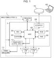
- Fig. 1 is a diagram of the overall configuration of an image forming apparatus.
- an image forming apparatus 1 and a personal computer (PC) 800 are connected such that communication is possible therebetween.
- a Web browser is installed on the PC 800.
- the Web browser receives, as an input, a uniform resource locater (URL), receives a Web page from a Web server (not illustrated), and can display a Web page on an operation unit (not illustrated) of the PC 800.
- a uniform resource locater URL
- the image forming apparatus 1 is equipped with a Web server for causing the user to set various settings of the image forming apparatus 1 through the Web browser of the PC 800.
- the Web browser of the PC 800 Upon input of an IP address or a host name of the image forming apparatus 1 in an address input field of the Web browser, the Web browser of the PC 800 receives a Web page for setting various settings from the image forming apparatus 1 and displays the Web page on a display unit. The user can set settings for the image forming apparatus 1 through the Web page for setting the various settings.
- the image forming apparatus 1 has a plurality of function units, a control unit 5, an operation unit 2, the printer unit 3, the scanner unit 4, and a power supply unit 113.
- the power supply unit 113 supplies power to the control unit 5, the operation unit 2, the printer unit 3, and the scanner unit 4.
- the operation unit 2 has a liquid crystal display unit having a touch panel and a keyboard.
- the operation unit 2 has a power-saving button for causing the power state of the image forming apparatus 1 to switch to a sleep state.
- the power-saving button is pressed in a standby state, the power state of the image forming apparatus 1 is switched to the sleep state, in which less power is consumed than in the standby state.
- the power-saving button is pressed in the sleep state, the power state of the image forming apparatus 1 is switched to the standby state.
- the sleep state described above is a sleep state in which power to the printer unit 3 or the scanner unit 4 is stopped
- the sleep state may be a deep sleep state in which power to the control unit 5 is stopped.
- the sleep state may also be a sleep state in which power supply to the control unit 5 is not stopped.
- the printer unit 3 prints an image on a sheet using image data received by the control unit 5.
- a printing system for the printer unit 3 an electrophotography system may be employed in which an image is printed by fixing toner on a sheet or an ink-jet system may also be employed in which an image is printed by discharging ink onto a sheet.
- the scanner unit 4 scans a document image and transmits image data of the scan image to the control unit 5.
- the control unit 5 has an application specific integrated circuit (ASIC) 100.
- the control unit 5 has a read-only memory (ROM) 600 and a random access memory (RAM) 500.
- the control unit 5 has a hard disk drive (HDD) 300, an electrically erasable programmable read-only memory (EEPROM) 400, and a network interface (I/F) 200.
- the control unit 5 has a power supply control circuit 112.
- the control unit 5 executes various functions of the image forming apparatus 1.
- the ASIC 100 reads out a control program stored in the ROM 600 or the HDD 300 and performs various types of control such as print control and scan control.
- the RAM 500 is a volatile memory and is a working memory used when the control program is executed.
- the HDD 300 is a storage medium such as a magnetic disk and stores, for example, the control program and image data.
- the EEPROM 400 is a nonvolatile memory and stores, for example, setting values to which reference is made when the control program is executed.
- the network I/F 200 receives print data and various data from the PC 800 via the network 700.
- the power supply control circuit 112 When receiving a switching request to the sleep state from, for example, the power-saving button, the power supply control circuit 112 stops power supply from the power supply unit (the power supply unit) 113 to the printer unit 3 and the scanner unit 4. As a result, the image forming apparatus 1 switches to the sleep state. In addition, when receiving a request to return from the sleep state from, for example, the power-saving button, the power supply control circuit 112 performs control such that power is supplied from the power supply unit 113 to the printer unit 3 and the scanner unit 4.
- Fig. 2 is a block diagram of the ASIC 100.
- the ASIC 100 has a main CPU (execution means) 101, a storage unit 102 for storing boot data for the main CPU 101, a sub-CPU (verification means) 103, and a storage unit 104 for storing boot data for the sub-CPU 103.
- the ASIC 100 has an input interface 105, an output interface 106, a data processing unit 107, a phase locked loop (PLL) 109, and a clock selecting unit (a signal selecting unit) 110.
- the ASIC 100 has a process information storage unit (a retaining unit) 111, a reset controller 114, and a power supply terminal 115.
- a clock signal output unit according to the present invention includes an oscillator 108, the PLL 109, and the clock selecting unit 110.
- the main CPU 101 controls devices inside the ASIC 100.
- the main CPU 101 can operate using a clock signal having a frequency of 1200 MHz in a case where a power-supply voltage of 1.0 V is applied thereto.
- a power-supply voltage of 1.0 V is applied thereto.
- the main CPU 101 is operable at 1200 MHz even when the power-supply voltage is less than 1.0 V, and there may also be a case where the main CPU 101 does not operate at 1200 MHz unless a power-supply voltage higher than 1.0 V is applied thereto.
- the storage unit 102 stores a program executed when the main CPU 101 boots up and various types of data used when the main CPU 101 boots up (hereinafter the program and various types of data are collectively referred to as boot data).
- the storage unit 102 is a read-only memory (ROM).
- the sub-CPU 103 performs auxiliary control for the main CPU 101.
- the storage unit 104 stores a program executed when the sub-CPU 103 boots up and various types of data used when the sub-CPU 103 boots up.
- the storage unit 104 is a ROM.
- the sub-CPU 103 boots up earlier than the main CPU 101. That is, when the image forming apparatus 1 is switched on (when the ASIC 100 is reset), the sub-CPU 103 boots up using the boot data stored in the storage unit 104, and performs verification of the boot data stored in the storage unit 102. As a result of the verification of the boot data by the sub-CPU 103, in a case where it is determined that the boot data to be executed by the main CPU 101 has not been tampered with, the main CPU 101 executes the boot program stored in the storage unit 102.
- the input interface (hereinafter referred to as I/F) 105 is an interface through which data is input from outside the ASIC 100.
- the output interface 106 is an interface through which data is output to the outside.
- the data processing unit 107 is a module that performs predetermined processing on data input from the input I/F 105.
- the data processing unit 107 receives image data and performs image processing (enlargement, reduction, correction, and the like) on the received image data.
- the oscillator 108 supplies a clock signal to the ASIC 100.
- the oscillator 108 supplies, for example, a clock signal having 10 MHz.
- the PLL 109 is a circuit that converts the frequency of the clock signal supplied from the oscillator 108 into a desired frequency and outputs the resulting clock signal.
- the PLL 109 converts the frequency (10 MHz) of an input clock signal into, for example, a 1200 MHz clock signal, which has a 120 times higher frequency, and outputs the 1200 MHz clock signal.
- the clock selecting unit (multiplexer (MUX)) 110 receives the clock signal supplied by the oscillator 108 and the clock signal supplied by the PLL 109.
- the clock selecting unit 110 outputs either of the clock signal supplied by the oscillator 108 and the clock signal supplied by the PLL 109.
- the clock selecting unit 110 outputs, in accordance with a command from the sub-CPU 103, either of the clock signal supplied by the oscillator 108 and the clock signal supplied by the PLL 109.
- the modules inside the ASIC 100 (the main CPU 101, the sub-CPU 103, the data processing unit 107, and other circuits) perform data reception and transmission therebetween in relation to synchronization, and thus the clock signals input to the modules need to be synchronized to each other.
- the clock signals to be supplied to the modules branch from the clock signal output from the clock selecting unit 110. As long as the phases of the clock signals input to the modules are synchronized with each other, the clock signals may have different frequencies.
- the process information storage unit 111 stores process information (3-bit information) regarding the main CPU 101.
- the process information storage unit 111 is a ROM.
- the power supply control circuit 112 changes the voltage to be output by the power supply unit 113.
- the power supply control circuit 112 changes the voltage to be output from the power supply unit 113, on the basis of the process information stored in the process information storage unit 111.
- the power supply unit 113 applies a voltage to the ASIC 100 via the power supply terminal 115.
- the power supply unit 113 applies a predetermined voltage to the ASIC 100 on the basis of a voltage control signal output from the power supply control circuit 112.
- the reset controller 114 outputs a reset signal to the modules inside the ASIC 100.
- the reset controller 114 cancels reset of the sub-CPU 103 and the storage unit 104.
- the reset controller 114 cancels reset of the main CPU 101.
- the ASIC 100 is operable in two operation modes, which are a slow-speed operation mode and a high-speed operation mode.
- the clock selecting unit 110 selects and outputs, in accordance with a command from the sub-CPU 103, the clock signal input from the oscillator 108.
- the output clock signal is used as a clock signal for operating the main CPU 101, the sub-CPU 103, and the data processing unit 107.
- the clock signal is input to circuits other than those described above.
- the clock signal output from the clock selecting unit 110 is directly supplied to the modules; however, a clock signal whose frequency has been reduced by using, for example, a frequency divider circuit may also be supplied to the modules.
- the clock selecting unit 110 selects and outputs, in accordance with a command from the sub-CPU 103, the clock signal input from the PLL 109.
- the output clock signal is used as a clock signal for operating the main CPU 101, the sub-CPU 103, and the data processing unit 107.
- the clock signal is input to circuits other than those described above.
- Fig. 3 is a flowchart illustrating processing executed by the sub-CPU 103.
- a reset signal is input to the ASIC 100.
- the ASIC 100 When the ASIC 100 is reset, the ASIC 100 enters the slow-speed operation mode on the basis of initial settings.
- the clock signal (10 MHz) output from the oscillator 108 is input to the sub-CPU 103 (S302).
- the reset controller 114 cancels reset of the sub-CPU 103 and the storage unit 104 using a hardware sequence. As a result, the sub-CPU 103 executes the boot data stored in the storage unit 104 (S303).
- the booted sub-CPU 103 sets settings such that the PLL 109 outputs a 1200 MHz clock signal. As a result, the PLL 109 causes a 1200 MHz clock signal to oscillate (S304).
- the sub-CPU 103 sets various parameters such that the data processing unit 107 executes predetermined processing (S305).
- the sub-CPU 103 determines whether a lock-up time for the PLL 109 has elapsed (S306).
- a lock-up time is a time required for the PLL 109 to cause a signal having a predetermined frequency (in this case, 1200 MHz) to stably oscillate.
- the sub-CPU 103 switches the output of the clock selecting unit 110 from the clock signal output from the oscillator 108 to the clock signal output from the PLL 109 (S307). As a result, the ASIC 100 enters the high-speed operation mode.
- the sub-CPU 103 then performs verification of the boot data for the main CPU 101 (S308). For example, the sub-CPU 103 compares a correct value prestored in the storage unit 104 with a hash value of the boot data stored in the storage unit 102. In a case where the correct value matches the hash value of the boot data, the sub-CPU 103 determines that the boot data has not been tampered with, and in a case where the correct value does not match the hash value of the boot data, the sub-CPU 103 determines that the boot data has been tampered with. Note that the boot-data tampering detection method will be described in detail with reference to Figs. 4 and 5 .
- the main CPU 101 does not execute the boot data, and the sub-CPU 103 notifies the user and the administrator that tampering has occurred (S310).
- the notification method for example, an unillustrated light-emitting diode (LED) (light output means) may be lit up or a sound notification may be used.
- LED light-emitting diode
- the sub-CPU 103 switches the output of the clock selecting unit 110 from the clock signal output from the PLL 109 to the clock signal output from the oscillator 108 (S311). As a result, the ASIC 100 enters the slow-speed operation mode.
- the sub-CPU 103 then cancels reset of the main CPU 101 and other circuits (S312). As a result, the main CPU 101 starts to boot up.
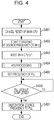
- Fig. 4 is a flowchart illustrating processing executed by the main CPU 101.
- the main CPU 101 When reset of the main CPU 101 is canceled (S401), the main CPU 101 starts operating using the clock signal output from the oscillator 108 (S402). The main CPU 101 executes the boot data stored in the storage unit 102 (S403). The boot data has been verified and it is determined that the boot data has not been tampered with. In the present embodiment, the main CPU 101 executes ASV processing (S404). Details of the ASV processing will be described with reference to Figs. 6 , 7 , and 8 .
- the main CPU 101 sets settings such that the PLL 109 outputs a 1200 MHz clock signal (S405). Thereafter, the main CPU 101 determines whether the lock-up time for the PLL 109 has elapsed (S406). In a case where it is determined that the lock-up time for the PLL 109 has elapsed (Yes in S406), the main CPU 101 switches the output of the clock selecting unit 110 from the clock signal output from the oscillator 108 to the clock signal output from the PLL 109 (S407). As a result, the ASIC 100 enters the high-speed operation mode. Thereafter, the main CPU 101 controls data processing performed at the data processing unit 107.
- the settings for various types of data processing to be executed at the data processing unit 107 are set as various settings for the ASIC 100.
- the power-supply voltage to the main CPU 101 is changed to a voltage suitable for processing to be performed by the main CPU 101, and thus the main CPU 101 can execute various types of data processing.
- the sub-CPU 103 can perform the tampering detection processing using the high frequency clock signal output from the PLL 109, and thus tampering detection processing can be completed in a short time.
- the clock signal supplied to the main CPU 101 is switched to the low frequency clock signal from the oscillator 108, and thus the main CPU 101 can perform the ASV processing.
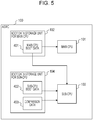
- Fig. 5 is a diagram illustrating details of blocks related to the verification of the boot program.
- the storage unit 102 stores boot data 401 for the main CPU 101.
- the main CPU 101 reads and executes the boot data 401 for the main CPU 101 stored in the storage unit 102.
- the storage unit 104 stores boot data 402 for the sub-CPU 103.
- the sub-CPU 103 reads and executes the boot data 402 for the sub-CPU 103 stored in the storage unit 104.
- the sub-CPU 103 starts to boot up.
- the storage unit 104 stores comparison data (a correct value) that is to be compared with the boot data 401 to be executed by the main CPU 101.
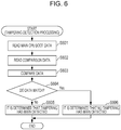
- Fig. 6 is a diagram illustrating a flowchart for a boot program verification method.
- the sub-CPU 103 reads a predetermined amount of data (for example, 100 kB) from the first data of the boot data 401 for the main CPU 101 stored in the storage unit 102 (S601).
- the read data is stored in a buffer memory of the sub-CPU 103.
- the sub-CPU 103 reads comparison data 403 as much as the data read from the storage unit 102 (S602).
- the sub-CPU 103 then compares the boot data 401 for the main CPU 101 stored in the buffer memory with the comparison data 403 (S603). As a result of the comparison, in a case where the boot data 401 differs from the comparison data 403 (No in S604), the sub-CPU 103 determines that the boot data 401 has been tampered with (S605).
- the sub-CPU 103 determines that the boot data 401 has not been tampered with (S606).
- the boot data 401 for the main CPU 101 itself is compared with the comparison data 403.
- a hash value of the boot data 401 for the main CPU 101 is calculated, and the verification of the boot data 401 may also be performed by comparing the hash value with the prestored correct value.
- the verification of part of the boot data 401 (100 kB) is performed; however, the verification of all the boot data 401 may also be performed.
- Fig. 7 is a diagram illustrating details of blocks related to the ASV processing.
- the process information storage unit 111 stores process information regarding the main CPU 101.
- the process information storage unit 111 is a ROM.
- the process for the main CPU 101 is classified into eight stages from slow to fast, 3-bit data is stored as information regarding the process in the process information storage unit 111.
- Fig. 8 is a diagram illustrating details of the information stored in the process information storage unit 111. As illustrated in Fig. 8 , a typical process is set to "4", and is represented as 3-bit data "100". The slowest process is set to "0”, and is represented as 3-bit data "000”. Moreover, the fastest process is set to "7”, and is represented as 3-bit data "111".
- the power supply control circuit 112 receives, from the main CPU 101, the process information stored in the process information storage unit 111. On the basis of the received process information, the power supply control circuit 112 outputs a control signal for changing the voltage to be output from the power supply unit 113.
- the main CPU 101 outputs the 3-bit data to the power supply control circuit 112.
- the ASIC 100 and the power supply control circuit 112 are connected by a serial bus.
- An I2C (I-squared-C) I/F unit 601 of the ASIC 100 and an I2C I/F unit 602 of the power supply control circuit 112 perform communication using the I2C protocol.
- a data processing unit 603 of the power supply control circuit 112 outputs, as a 3-bit control signal, 3-bit process information input via the I2C I/F unit 602 to the power supply unit 113.
- the power supply unit 113 When the image forming apparatus 1 is switched on, the power supply unit 113 outputs a typical voltage, that is, a voltage of 1.0 V in the present embodiment. Thereafter, the power supply unit 113 applies a predetermined voltage to the power supply terminal 115 on the basis of the control signal input from the power supply control circuit 112. For example, as illustrated in Fig. 8 , in a case where the main CPU 101 is a typical chip, the 3-bit data output from the process information storage unit 111 is "100". The power-supply voltage applied to the main CPU 101 is 1.0 V.
- the 3-bit data output from the process information storage unit 111 is "000".
- the power-supply voltage applied to the main CPU 101 is 1.12V (see Fig. 8 ).
- the 3-bit data output from the process information storage unit 111 is "111".
- the power-supply voltage applied to the main CPU 101 is 0.91 V (see Fig. 8 ).
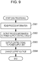
- Fig. 9 is a flowchart illustrating details of the ASV processing.
- the main CPU 101 reads process information recorded in three bits from the process information storage unit 111 (S901). In the present embodiment, the process information regarding the main CPU 101 and recorded in three bits is read by reading out data at a specific address of the process information storage unit 111.
- the main CPU 101 outputs the 3-bit process information to the power supply control circuit 112 (S902). In the present embodiment, the main CPU 101 transmits the process information in accordance with the I2C protocol.
- the power supply control circuit 112 receives the 3-bit process information input from the ASIC 100.
- the data processing unit 603 outputs a control signal for changing the output voltage of the power supply unit 113 to the power supply unit 113 (S903).
- the power supply unit 113 is provided with a 3-bit input terminal for controlling the output voltage.
- the power supply unit 113 adjusts, on the basis of the control signal input to the input terminal, the power-supply voltage to be applied to the main CPU 101 (S904).
- the relationship between the 3-bit control signal and the power-supply voltage output from the power supply unit 113 is illustrated in Fig. 8 .
- the power supply unit 113 In a case where the 3-bit data is "100”, the power supply unit 113 outputs 1.0 V to the main CPU 101. In addition, in a case where the 3-bit data is "110", the power supply unit 113 outputs 0.94 V to the main CPU 101.
- the clock selecting unit 110 outputs either the clock signal supplied from the oscillator 108 or the clock signal supplied from the PLL 109.
- the clock selecting unit 110 may receive three or more clock signals having different frequencies and may output any one of the clock signals.
- the clock selecting unit 110 outputs a 1200 MHz clock signal to the sub-CPU 103 when the sub-CPU 103 performs verification of the boot data, and outputs a 10 MHz clock signal to the main CPU 101 when the main CPU 101 performs the ASV processing.
- the clock selecting unit 110 then outputs a 1200 MHz clock signal to the main CPU 101 when the ASV processing is completed.
- the frequencies are not limited to 10 MHz and 1200 MHz.
- the frequency of the clock signal at the time when the verification of the boot data is performed does not have to be the same as the frequency of the clock signal after the ASV processing is completed.
- the present invention provides an information processing apparatus capable of shortening a time required for tampering detection processing.
- Embodiments of the present invention can also be realized by a computer of a system or apparatus that reads out and executes computer executable instructions (e.g., one or more programs) recorded on a storage medium (which may also be referred to more fully as a 'non-transitory computer-readable storage medium') to perform the functions of one or more of the above-described embodiments and/or that includes one or more circuits (e.g., application specific integrated circuit (ASIC)) for performing the functions of one or more of the above-described embodiments, and by a method performed by the computer of the system or apparatus by, for example, reading out and executing the computer executable instructions from the storage medium to perform the functions of one or more of the above-described embodiments and/or controlling the one or more circuits to perform the functions of one or more of the above-described embodiments.
- ASIC application specific integrated circuit
- the computer may comprise one or more processors (e.g., central processing unit (CPU), micro processing unit (MPU)) and may include a network of separate computers or separate processors to read out and execute the computer executable instructions.
- the computer executable instructions may be provided to the computer, for example, from a network or the storage medium.
- the storage medium may include, for example, one or more of a hard disk, a random-access memory (RAM), a read only memory (ROM), a storage of distributed computing systems, an optical disk (such as a compact disc (CD), digital versatile disc (DVD), or Blu-ray Disc (BD)TM), a flash memory device, a memory card, and the like.
Landscapes
- Engineering & Computer Science (AREA)
- Theoretical Computer Science (AREA)
- Computer Security & Cryptography (AREA)
- General Engineering & Computer Science (AREA)
- Software Systems (AREA)
- Physics & Mathematics (AREA)
- General Physics & Mathematics (AREA)
- Computer Hardware Design (AREA)
- Signal Processing (AREA)
- Multimedia (AREA)
- Human Computer Interaction (AREA)
- Health & Medical Sciences (AREA)
- General Health & Medical Sciences (AREA)
- Virology (AREA)
- Computing Systems (AREA)
- Power Sources (AREA)
- Facsimiles In General (AREA)
- Accessory Devices And Overall Control Thereof (AREA)
Abstract
Description
- The present invention relates to an information processing apparatus capable of detecting software tampering and the like.
- An information processing apparatus is known that detects software tampering (hereinafter referred to as tampering detection) and prohibits execution of software for which tampering is detected. For example, a sub central processing unit (CPU) performs verification of software to be executed by a main CPU, and the main CPU executes software that has been successfully verified. When the software is not successfully verified, execution of the software is prohibited.
- In addition, some information processing apparatuses are equipped with a technology called adaptive supply voltage (ASV) in which a power-supply voltage is changed in accordance with variations from device to device (for example, from CPU to CPU) (Japanese Patent Laid-Open No.
2005-322860 - In a case where a device is a slow device, operation of the device may be unstable unless a voltage necessary for the device is input and then a clock signal having a predetermined frequency is input. Thus, until the voltage necessary for the device is input, a clock signal having a frequency lower than the predetermined frequency is input. After the voltage necessary for the device is input, the clock signal having the predetermined frequency is input to the device using, for example, a phase-locked loop circuit (hereinafter referred to as a PLL circuit).
- As described above, due to ASV processing, until a voltage necessary for a device is input, a slow clock signal needs to be input in order to operate the device with certainty. Thus, tampering detection processing that is processing executed before the device operates and that is for software to be executed by the device is executed using the slow clock signal. As a result, the tampering detection processing takes a longer time.
- The present invention provides an information processing apparatus capable of shortening a time required for tampering detection processing.
- The present invention in its first aspect provides an information processing apparatus as specified in
claims 1 to 19. - The present invention in its second aspect provides a control method as specified in claim 20.
- Further features of the present invention will become apparent from the following description of exemplary embodiments with reference to the attached drawings.
-
-
Fig. 1 is a diagram of the overall configuration of an image forming apparatus. -
Fig. 2 is a block diagram of an application specific integrated circuit (ASIC). -
Fig. 3 is a flowchart illustrating processing executed by a sub central processing unit (CPU). -
Fig. 4 is a flowchart illustrating processing executed by a main CPU. -
Fig. 5 is a diagram illustrating details of blocks related to verification of a boot program. -
Fig. 6 is a diagram illustrating a flowchart for a boot program verification method. -
Fig. 7 is a diagram illustrating details of blocks related to ASV processing. -
Fig. 8 is a diagram illustrating details of information stored in a process information storage unit. -
Fig. 9 is a flowchart illustrating details of the ASV processing. - In the following, embodiments of the present invention will be described in detail with reference to the drawings.
- In the present embodiment, as an information processing apparatus, an image forming apparatus having a print function and a scan function will be described as an example.
-
Fig. 1 is a diagram of the overall configuration of an image forming apparatus. - To a
network 700, animage forming apparatus 1 and a personal computer (PC) 800 are connected such that communication is possible therebetween. In addition, a Web browser is installed on the PC 800. The Web browser receives, as an input, a uniform resource locater (URL), receives a Web page from a Web server (not illustrated), and can display a Web page on an operation unit (not illustrated) of the PC 800. - The
image forming apparatus 1 is equipped with a Web server for causing the user to set various settings of theimage forming apparatus 1 through the Web browser of the PC 800. Upon input of an IP address or a host name of theimage forming apparatus 1 in an address input field of the Web browser, the Web browser of the PC 800 receives a Web page for setting various settings from theimage forming apparatus 1 and displays the Web page on a display unit. The user can set settings for theimage forming apparatus 1 through the Web page for setting the various settings. - Next, the configuration of the
image forming apparatus 1 will be described. Theimage forming apparatus 1 has a plurality of function units, acontrol unit 5, anoperation unit 2, theprinter unit 3, thescanner unit 4, and apower supply unit 113. - The
power supply unit 113 supplies power to thecontrol unit 5, theoperation unit 2, theprinter unit 3, and thescanner unit 4. Theoperation unit 2 has a liquid crystal display unit having a touch panel and a keyboard. In addition, theoperation unit 2 has a power-saving button for causing the power state of theimage forming apparatus 1 to switch to a sleep state. When the power-saving button is pressed in a standby state, the power state of theimage forming apparatus 1 is switched to the sleep state, in which less power is consumed than in the standby state. In addition, when the power-saving button is pressed in the sleep state, the power state of theimage forming apparatus 1 is switched to the standby state. As long as the sleep state described above is a sleep state in which power to theprinter unit 3 or thescanner unit 4 is stopped, the sleep state may be a deep sleep state in which power to thecontrol unit 5 is stopped. In addition, the sleep state may also be a sleep state in which power supply to thecontrol unit 5 is not stopped. - In accordance with a print command received from the user, the
printer unit 3 prints an image on a sheet using image data received by thecontrol unit 5. As a printing system for theprinter unit 3, an electrophotography system may be employed in which an image is printed by fixing toner on a sheet or an ink-jet system may also be employed in which an image is printed by discharging ink onto a sheet. In accordance with a scan command received from the user, thescanner unit 4 scans a document image and transmits image data of the scan image to thecontrol unit 5. - The
control unit 5 has an application specific integrated circuit (ASIC) 100. In addition, thecontrol unit 5 has a read-only memory (ROM) 600 and a random access memory (RAM) 500. Thecontrol unit 5 has a hard disk drive (HDD) 300, an electrically erasable programmable read-only memory (EEPROM) 400, and a network interface (I/F) 200. In addition, thecontrol unit 5 has a powersupply control circuit 112. - The
control unit 5 executes various functions of theimage forming apparatus 1. The ASIC 100 reads out a control program stored in theROM 600 or theHDD 300 and performs various types of control such as print control and scan control. TheRAM 500 is a volatile memory and is a working memory used when the control program is executed. The HDD 300 is a storage medium such as a magnetic disk and stores, for example, the control program and image data. The EEPROM 400 is a nonvolatile memory and stores, for example, setting values to which reference is made when the control program is executed. - The network I/
F 200 receives print data and various data from the PC 800 via thenetwork 700. - When receiving a switching request to the sleep state from, for example, the power-saving button, the power
supply control circuit 112 stops power supply from the power supply unit (the power supply unit) 113 to theprinter unit 3 and thescanner unit 4. As a result, theimage forming apparatus 1 switches to the sleep state. In addition, when receiving a request to return from the sleep state from, for example, the power-saving button, the powersupply control circuit 112 performs control such that power is supplied from thepower supply unit 113 to theprinter unit 3 and thescanner unit 4. -
Fig. 2 is a block diagram of theASIC 100. - The
ASIC 100 has a main CPU (execution means) 101, astorage unit 102 for storing boot data for themain CPU 101, a sub-CPU (verification means) 103, and astorage unit 104 for storing boot data for thesub-CPU 103. In addition, theASIC 100 has aninput interface 105, anoutput interface 106, adata processing unit 107, a phase locked loop (PLL) 109, and a clock selecting unit (a signal selecting unit) 110. In addition, theASIC 100 has a process information storage unit (a retaining unit) 111, areset controller 114, and apower supply terminal 115. A clock signal output unit according to the present invention includes anoscillator 108, thePLL 109, and theclock selecting unit 110. - The
main CPU 101 controls devices inside theASIC 100. Basically, themain CPU 101 can operate using a clock signal having a frequency of 1200 MHz in a case where a power-supply voltage of 1.0 V is applied thereto. However, depending on device variations, there may be a case where themain CPU 101 is operable at 1200 MHz even when the power-supply voltage is less than 1.0 V, and there may also be a case where themain CPU 101 does not operate at 1200 MHz unless a power-supply voltage higher than 1.0 V is applied thereto. - The
storage unit 102 stores a program executed when themain CPU 101 boots up and various types of data used when themain CPU 101 boots up (hereinafter the program and various types of data are collectively referred to as boot data). Thestorage unit 102 is a read-only memory (ROM). - The
sub-CPU 103 performs auxiliary control for themain CPU 101. - The
storage unit 104 stores a program executed when the sub-CPU 103 boots up and various types of data used when the sub-CPU 103 boots up. Thestorage unit 104 is a ROM. - In the present embodiment, when the
image forming apparatus 1 is switched on (when theASIC 100 is reset), the sub-CPU 103 boots up earlier than themain CPU 101. That is, when theimage forming apparatus 1 is switched on (when theASIC 100 is reset), the sub-CPU 103 boots up using the boot data stored in thestorage unit 104, and performs verification of the boot data stored in thestorage unit 102. As a result of the verification of the boot data by thesub-CPU 103, in a case where it is determined that the boot data to be executed by themain CPU 101 has not been tampered with, themain CPU 101 executes the boot program stored in thestorage unit 102. - The input interface (hereinafter referred to as I/F) 105 is an interface through which data is input from outside the
ASIC 100. Theoutput interface 106 is an interface through which data is output to the outside. - The
data processing unit 107 is a module that performs predetermined processing on data input from the input I/F 105. For example, thedata processing unit 107 receives image data and performs image processing (enlargement, reduction, correction, and the like) on the received image data. - The
oscillator 108 supplies a clock signal to theASIC 100. Theoscillator 108 supplies, for example, a clock signal having 10 MHz. ThePLL 109 is a circuit that converts the frequency of the clock signal supplied from theoscillator 108 into a desired frequency and outputs the resulting clock signal. ThePLL 109 converts the frequency (10 MHz) of an input clock signal into, for example, a 1200 MHz clock signal, which has a 120 times higher frequency, and outputs the 1200 MHz clock signal. - The clock selecting unit (multiplexer (MUX)) 110 receives the clock signal supplied by the
oscillator 108 and the clock signal supplied by thePLL 109. Theclock selecting unit 110 outputs either of the clock signal supplied by theoscillator 108 and the clock signal supplied by thePLL 109. In the present embodiment, theclock selecting unit 110 outputs, in accordance with a command from the sub-CPU 103, either of the clock signal supplied by theoscillator 108 and the clock signal supplied by thePLL 109. The modules inside the ASIC 100 (themain CPU 101, the sub-CPU 103, thedata processing unit 107, and other circuits) perform data reception and transmission therebetween in relation to synchronization, and thus the clock signals input to the modules need to be synchronized to each other. In the present embodiment, the clock signals to be supplied to the modules branch from the clock signal output from theclock selecting unit 110. As long as the phases of the clock signals input to the modules are synchronized with each other, the clock signals may have different frequencies. - The process
information storage unit 111 stores process information (3-bit information) regarding themain CPU 101. The processinformation storage unit 111 is a ROM. - The power
supply control circuit 112 changes the voltage to be output by thepower supply unit 113. The powersupply control circuit 112 changes the voltage to be output from thepower supply unit 113, on the basis of the process information stored in the processinformation storage unit 111. Thepower supply unit 113 applies a voltage to theASIC 100 via thepower supply terminal 115. Thepower supply unit 113 applies a predetermined voltage to theASIC 100 on the basis of a voltage control signal output from the powersupply control circuit 112. - The
reset controller 114 outputs a reset signal to the modules inside theASIC 100. When theimage forming apparatus 1 is switched on (when theASIC 100 is reset), thereset controller 114 cancels reset of the sub-CPU 103 and thestorage unit 104. Next, in accordance with a command from the sub-CPU 103, thereset controller 114 cancels reset of themain CPU 101. - The
ASIC 100 is operable in two operation modes, which are a slow-speed operation mode and a high-speed operation mode. In the slow-speed operation mode, theclock selecting unit 110 selects and outputs, in accordance with a command from the sub-CPU 103, the clock signal input from theoscillator 108. As illustrated inFig. 2 , the output clock signal is used as a clock signal for operating themain CPU 101, the sub-CPU 103, and thedata processing unit 107. In addition, although not illustrated inFig. 2 , the clock signal is input to circuits other than those described above. - In
Fig. 2 , the clock signal output from theclock selecting unit 110 is directly supplied to the modules; however, a clock signal whose frequency has been reduced by using, for example, a frequency divider circuit may also be supplied to the modules. - In the high-speed operation mode, the
clock selecting unit 110 selects and outputs, in accordance with a command from the sub-CPU 103, the clock signal input from thePLL 109. As illustrated inFig. 2 , the output clock signal is used as a clock signal for operating themain CPU 101, the sub-CPU 103, and thedata processing unit 107. In addition, although not illustrated inFig. 2 , the clock signal is input to circuits other than those described above. -
Fig. 3 is a flowchart illustrating processing executed by thesub-CPU 103. - When the image forming apparatus is switched on by the user (S301), a reset signal is input to the
ASIC 100. When theASIC 100 is reset, theASIC 100 enters the slow-speed operation mode on the basis of initial settings. The clock signal (10 MHz) output from theoscillator 108 is input to the sub-CPU 103 (S302). Thereset controller 114 cancels reset of the sub-CPU 103 and thestorage unit 104 using a hardware sequence. As a result, thesub-CPU 103 executes the boot data stored in the storage unit 104 (S303). - The booted
sub-CPU 103 sets settings such that thePLL 109 outputs a 1200 MHz clock signal. As a result, thePLL 109 causes a 1200 MHz clock signal to oscillate (S304). - Thereafter, the sub-CPU 103 sets various parameters such that the
data processing unit 107 executes predetermined processing (S305). The sub-CPU 103 then determines whether a lock-up time for thePLL 109 has elapsed (S306). A lock-up time is a time required for thePLL 109 to cause a signal having a predetermined frequency (in this case, 1200 MHz) to stably oscillate. - In a case where it is determined that the lock-up time has elapsed (Yes in S306), the sub-CPU 103 switches the output of the
clock selecting unit 110 from the clock signal output from theoscillator 108 to the clock signal output from the PLL 109 (S307). As a result, theASIC 100 enters the high-speed operation mode. - In the present embodiment, the sub-CPU 103 then performs verification of the boot data for the main CPU 101 (S308). For example, the
sub-CPU 103 compares a correct value prestored in thestorage unit 104 with a hash value of the boot data stored in thestorage unit 102. In a case where the correct value matches the hash value of the boot data, thesub-CPU 103 determines that the boot data has not been tampered with, and in a case where the correct value does not match the hash value of the boot data, thesub-CPU 103 determines that the boot data has been tampered with. Note that the boot-data tampering detection method will be described in detail with reference toFigs. 4 and5 . - In a case where it is determined that the boot data has been tampered with (Yes in S309), the
main CPU 101 does not execute the boot data, and thesub-CPU 103 notifies the user and the administrator that tampering has occurred (S310). As the notification method, for example, an unillustrated light-emitting diode (LED) (light output means) may be lit up or a sound notification may be used. - In a case where it is determined that the boot data has not been tampered with (No in S309), the sub-CPU 103 switches the output of the
clock selecting unit 110 from the clock signal output from thePLL 109 to the clock signal output from the oscillator 108 (S311). As a result, theASIC 100 enters the slow-speed operation mode. - The sub-CPU 103 then cancels reset of the
main CPU 101 and other circuits (S312). As a result, themain CPU 101 starts to boot up. -
Fig. 4 is a flowchart illustrating processing executed by themain CPU 101. - When reset of the
main CPU 101 is canceled (S401), themain CPU 101 starts operating using the clock signal output from the oscillator 108 (S402). Themain CPU 101 executes the boot data stored in the storage unit 102 (S403). The boot data has been verified and it is determined that the boot data has not been tampered with. In the present embodiment, themain CPU 101 executes ASV processing (S404). Details of the ASV processing will be described with reference toFigs. 6 ,7 , and8 . - When the ASV processing ends, the
main CPU 101 sets settings such that thePLL 109 outputs a 1200 MHz clock signal (S405). Thereafter, themain CPU 101 determines whether the lock-up time for thePLL 109 has elapsed (S406). In a case where it is determined that the lock-up time for thePLL 109 has elapsed (Yes in S406), themain CPU 101 switches the output of theclock selecting unit 110 from the clock signal output from theoscillator 108 to the clock signal output from the PLL 109 (S407). As a result, theASIC 100 enters the high-speed operation mode. Thereafter, themain CPU 101 controls data processing performed at thedata processing unit 107. - At the time when the
ASIC 100 enters the high-speed operation mode, the settings for various types of data processing to be executed at thedata processing unit 107 are set as various settings for theASIC 100. In addition, the power-supply voltage to themain CPU 101 is changed to a voltage suitable for processing to be performed by themain CPU 101, and thus themain CPU 101 can execute various types of data processing. - In accordance with the flowchart above, before the
main CPU 101 performs the ASV processing, the sub-CPU 103 can perform the tampering detection processing using the high frequency clock signal output from thePLL 109, and thus tampering detection processing can be completed in a short time. In addition, after the sub-CPU 103 ends the tampering detection processing, the clock signal supplied to themain CPU 101 is switched to the low frequency clock signal from theoscillator 108, and thus themain CPU 101 can perform the ASV processing. - Next, the details of the tampering detection processing for a boot program in S308 of
Fig. 3 will be described.Fig. 5 is a diagram illustrating details of blocks related to the verification of the boot program. - The
storage unit 102 stores bootdata 401 for themain CPU 101. When reset of themain CPU 101 is canceled, themain CPU 101 reads and executes theboot data 401 for themain CPU 101 stored in thestorage unit 102. As a result, themain CPU 101 starts to boot up. Thestorage unit 104 stores bootdata 402 for thesub-CPU 103. When reset of thesub-CPU 103 is canceled, the sub-CPU 103 reads and executes theboot data 402 for the sub-CPU 103 stored in thestorage unit 104. As a result, the sub-CPU 103 starts to boot up. - In addition, the
storage unit 104 stores comparison data (a correct value) that is to be compared with theboot data 401 to be executed by themain CPU 101. -
Fig. 6 is a diagram illustrating a flowchart for a boot program verification method. - The sub-CPU 103 reads a predetermined amount of data (for example, 100 kB) from the first data of the
boot data 401 for themain CPU 101 stored in the storage unit 102 (S601). The read data is stored in a buffer memory of thesub-CPU 103. The sub-CPU 103 readscomparison data 403 as much as the data read from the storage unit 102 (S602). The sub-CPU 103 then compares theboot data 401 for themain CPU 101 stored in the buffer memory with the comparison data 403 (S603). As a result of the comparison, in a case where theboot data 401 differs from the comparison data 403 (No in S604), thesub-CPU 103 determines that theboot data 401 has been tampered with (S605). - In contrast, as a result of the comparison, in a case where the
boot data 401 matches the comparison data 403 (Yes in S604), thesub-CPU 103 determines that theboot data 401 has not been tampered with (S606). - In the present embodiment, the
boot data 401 for themain CPU 101 itself is compared with thecomparison data 403. However, a hash value of theboot data 401 for themain CPU 101 is calculated, and the verification of theboot data 401 may also be performed by comparing the hash value with the prestored correct value. - In addition, in the present embodiment, the verification of part of the boot data 401 (100 kB) is performed; however, the verification of all the
boot data 401 may also be performed. - Next, details of the ASV processing in S404 of
Fig. 4 will be described.Fig. 7 is a diagram illustrating details of blocks related to the ASV processing. - The process
information storage unit 111 stores process information regarding themain CPU 101. The processinformation storage unit 111 is a ROM. In the present embodiment, the process for themain CPU 101 is classified into eight stages from slow to fast, 3-bit data is stored as information regarding the process in the processinformation storage unit 111. -
Fig. 8 is a diagram illustrating details of the information stored in the processinformation storage unit 111. As illustrated inFig. 8 , a typical process is set to "4", and is represented as 3-bit data "100". The slowest process is set to "0", and is represented as 3-bit data "000". Moreover, the fastest process is set to "7", and is represented as 3-bit data "111". - Returning to
Fig. 7 , the powersupply control circuit 112 receives, from themain CPU 101, the process information stored in the processinformation storage unit 111. On the basis of the received process information, the powersupply control circuit 112 outputs a control signal for changing the voltage to be output from thepower supply unit 113. Themain CPU 101 outputs the 3-bit data to the powersupply control circuit 112. TheASIC 100 and the powersupply control circuit 112 are connected by a serial bus. An I2C (I-squared-C) I/F unit 601 of theASIC 100 and an I2C I/F unit 602 of the powersupply control circuit 112 perform communication using the I2C protocol. - A
data processing unit 603 of the powersupply control circuit 112 outputs, as a 3-bit control signal, 3-bit process information input via the I2C I/F unit 602 to thepower supply unit 113. When theimage forming apparatus 1 is switched on, thepower supply unit 113 outputs a typical voltage, that is, a voltage of 1.0 V in the present embodiment. Thereafter, thepower supply unit 113 applies a predetermined voltage to thepower supply terminal 115 on the basis of the control signal input from the powersupply control circuit 112. For example, as illustrated inFig. 8 , in a case where themain CPU 101 is a typical chip, the 3-bit data output from the processinformation storage unit 111 is "100". The power-supply voltage applied to themain CPU 101 is 1.0 V. In addition, in a case where themain CPU 101 performs the slowest process, the 3-bit data output from the processinformation storage unit 111 is "000". The power-supply voltage applied to themain CPU 101 is 1.12V (seeFig. 8 ). In addition, in a case where themain CPU 101 performs the fastest process, the 3-bit data output from the processinformation storage unit 111 is "111". The power-supply voltage applied to themain CPU 101 is 0.91 V (seeFig. 8 ). -
Fig. 9 is a flowchart illustrating details of the ASV processing. - The
main CPU 101 reads process information recorded in three bits from the process information storage unit 111 (S901). In the present embodiment, the process information regarding themain CPU 101 and recorded in three bits is read by reading out data at a specific address of the processinformation storage unit 111. Themain CPU 101 outputs the 3-bit process information to the power supply control circuit 112 (S902). In the present embodiment, themain CPU 101 transmits the process information in accordance with the I2C protocol. - The power
supply control circuit 112 receives the 3-bit process information input from theASIC 100. Thedata processing unit 603 outputs a control signal for changing the output voltage of thepower supply unit 113 to the power supply unit 113 (S903). Thepower supply unit 113 is provided with a 3-bit input terminal for controlling the output voltage. Thepower supply unit 113 adjusts, on the basis of the control signal input to the input terminal, the power-supply voltage to be applied to the main CPU 101 (S904). - The relationship between the 3-bit control signal and the power-supply voltage output from the
power supply unit 113 is illustrated inFig. 8 . In a case where the 3-bit data is "100", thepower supply unit 113 outputs 1.0 V to themain CPU 101. In addition, in a case where the 3-bit data is "110", thepower supply unit 113 outputs 0.94 V to themain CPU 101. - In the embodiment described above, the
clock selecting unit 110 outputs either the clock signal supplied from theoscillator 108 or the clock signal supplied from thePLL 109. Theclock selecting unit 110 may receive three or more clock signals having different frequencies and may output any one of the clock signals. - For example, the
clock selecting unit 110 outputs a 1200 MHz clock signal to the sub-CPU 103 when the sub-CPU 103 performs verification of the boot data, and outputs a 10 MHz clock signal to themain CPU 101 when themain CPU 101 performs the ASV processing. Theclock selecting unit 110 then outputs a 1200 MHz clock signal to themain CPU 101 when the ASV processing is completed. As long as the frequency of the clock signal output from theclock selecting unit 110 is high, then low, and then high, the frequencies are not limited to 10 MHz and 1200 MHz. The frequency of the clock signal at the time when the verification of the boot data is performed does not have to be the same as the frequency of the clock signal after the ASV processing is completed. - The present invention provides an information processing apparatus capable of shortening a time required for tampering detection processing.
- Embodiments of the present invention can also be realized by a computer of a system or apparatus that reads out and executes computer executable instructions (e.g., one or more programs) recorded on a storage medium (which may also be referred to more fully as a 'non-transitory computer-readable storage medium') to perform the functions of one or more of the above-described embodiments and/or that includes one or more circuits (e.g., application specific integrated circuit (ASIC)) for performing the functions of one or more of the above-described embodiments, and by a method performed by the computer of the system or apparatus by, for example, reading out and executing the computer executable instructions from the storage medium to perform the functions of one or more of the above-described embodiments and/or controlling the one or more circuits to perform the functions of one or more of the above-described embodiments. The computer may comprise one or more processors (e.g., central processing unit (CPU), micro processing unit (MPU)) and may include a network of separate computers or separate processors to read out and execute the computer executable instructions. The computer executable instructions may be provided to the computer, for example, from a network or the storage medium. The storage medium may include, for example, one or more of a hard disk, a random-access memory (RAM), a read only memory (ROM), a storage of distributed computing systems, an optical disk (such as a compact disc (CD), digital versatile disc (DVD), or Blu-ray Disc (BD)™), a flash memory device, a memory card, and the like.
- While the present invention has been described with reference to exemplary embodiments, it is to be understood that the invention is not limited to the disclosed exemplary embodiments. The scope of the following claims is to be accorded the broadest interpretation so as to encompass all such modifications and equivalent structures and functions.
Claims (20)
- An information processing apparatus comprising:execution means (101) configured to execute predetermined software;verification means (103) configured to perform verification of the predetermined software;power supply means (113) configured to output a voltage to the execution means (101);retaining means (111) configured to retain information corresponding to a voltage that is supposed to be applied to the execution means (101), wherein the execution means (101) sets the voltage to be output by the power supply means (113) on the basis of the information retained by the retaining means (111); andclock signal output means (108, 109, 110) configured to output a clock signal having a first frequency to the verification means (103) at least during verification processing of the predetermined software, the verification processing being performed by the verification means (103), and output a clock signal having a second frequency lower than the first frequency to the execution means (101) at least during setting processing of the voltage to be output by the power supply means (113), the setting processing being performed by the execution means (101).
- The information processing apparatus according to Claim 1, wherein the clock signal output means (108, 109, 110) outputs a clock signal having a third frequency higher than the second frequency after the voltage to be output by the power supply means (113) is set by the execution means (101).
- The information processing apparatus according to Claim 2, wherein the first frequency is the same as the third frequency.
- The information processing apparatus according to Claim 1, wherein the clock signal output means (108, 109, 110) receives the clock signal having the first frequency and the clock signal having the second frequency, and outputs either of the clock signal having the first frequency and the clock signal having the second frequency.
- The information processing apparatus according to Claim 4, further comprising: signal output means (108) configured to output the clock signal having the first frequency.
- The information processing apparatus according to Claim 5, further comprising: frequency change means (109) configured to receive the clock signal having the first frequency and output the clock signal having the second frequency.
- The information processing apparatus according to Claim 1, wherein, before verification is performed by the verification means (103), the clock signal output means (108, 109, 110) outputs a clock signal having a fourth frequency lower than the first frequency to the verification means (103).
- The information processing apparatus according to Claim 1, wherein the verification means (103) sets a frequency to be output by the clock signal output means (108, 109, 110).
- The information processing apparatus according to Claim 1, wherein the clock signal output means (108, 109, 110) outputs the clock signal having the second frequency in a case where the software is successfully verified by the verification means (103).
- The information processing apparatus according to Claim 1, further comprising: notification means (103) configured to send information indicating that the software is not successfully verified by the verification means (103).
- The information processing apparatus according to Claim 10, wherein the notification means (103) is light output means configured to output light.
- The information processing apparatus according to Claim 1, wherein the verification means (103) performs verification of the software by comparing a portion of the software to be executed by the execution means (101) with a prestored correction value.
- The information processing apparatus according to Claim 1, wherein the clock signal output means (108, 109, 110) outputs the clock signal having the first frequency and the clock signal having the second frequency to the execution means (101) and the verification means (103).
- The information processing apparatus according to Claim 1, wherein verification processing of the predetermined software is at least one of processing for reading the predetermined software, processing for reading comparison data to be compared with a value corresponding to the predetermined software, processing for comparing the value corresponding to the predetermined software with the comparison data, and processing for determining whether the value corresponding to the predetermined software matches the comparison data, the verification processing being performed by the verification means (103).
- The information processing apparatus according to Claim 1, wherein setting processing of the voltage to be output by the power supply means (113) is at least one of processing for reading information corresponding to the voltage from the retaining means (111) and processing for outputting to the power supply means (113) the information read from the retaining means (111), the setting processing being performed by the execution means (101).
- The information processing apparatus according to Claim 1, wherein the execution means (101) and the verification means (103) have a synchronization relationship.
- The information processing apparatus according to Claim 1, wherein the software is boot data for the execution means (101).
- The information processing apparatus according to Claim 1, further comprising: print means (3) configured to print an image on a sheet.
- The information processing apparatus according to Claim 1, further comprising: scanning means (4) configured to scan an image of a document.
- A control method for an information processing apparatus, comprising:outputting (S904) a voltage to execution means (101);performing (S308) verification of predetermined software to be executed by the execution means (101);retaining (S901) information corresponding to a voltage that is supposed to be applied to the execution means (101);setting (S904), on the basis of the retained information, the voltage to be applied to the execution means (101);outputting (S307) a clock signal having a first frequency to verification means (103) configured to perform verification of the predetermined software at least during verification processing of the software; andoutputting (S402) a clock signal having a second frequency lower than the first frequency to the execution means (101) at least during setting processing of the voltage that is supposed to be applied to the execution means (101).
Applications Claiming Priority (1)
| Application Number | Priority Date | Filing Date | Title |
|---|---|---|---|
| JP2018213732A JP7166884B2 (en) | 2018-11-14 | 2018-11-14 | Information processing equipment capable of detecting falsification of software |
Publications (2)
| Publication Number | Publication Date |
|---|---|
| EP3654134A1 true EP3654134A1 (en) | 2020-05-20 |
| EP3654134B1 EP3654134B1 (en) | 2025-04-09 |
Family
ID=68502905
Family Applications (1)
| Application Number | Title | Priority Date | Filing Date |
|---|---|---|---|
| EP19207691.7A Active EP3654134B1 (en) | 2018-11-14 | 2019-11-07 | Information processing apparatus capable of detecting software tampering and control method therefor |
Country Status (4)
| Country | Link |
|---|---|
| US (1) | US11403399B2 (en) |
| EP (1) | EP3654134B1 (en) |
| JP (1) | JP7166884B2 (en) |
| CN (1) | CN111191223B (en) |
Families Citing this family (4)
| Publication number | Priority date | Publication date | Assignee | Title |
|---|---|---|---|---|
| JP7011373B2 (en) * | 2018-07-11 | 2022-01-26 | キヤノン株式会社 | Multifunction device and its control method, and program |
| JP7278753B2 (en) * | 2018-11-19 | 2023-05-22 | キヤノン株式会社 | Information processing equipment capable of detecting falsification of software |
| JP7316902B2 (en) * | 2019-10-16 | 2023-07-28 | キヤノン株式会社 | Information processing device, its control method, and program |
| US20250278223A1 (en) * | 2023-12-19 | 2025-09-04 | Lexmark International, Inc. | Methods and systems for detection of clock tampering on an electronic device |
Citations (5)
| Publication number | Priority date | Publication date | Assignee | Title |
|---|---|---|---|---|
| JP2005322860A (en) | 2004-05-11 | 2005-11-17 | Sony Corp | Semiconductor integrated circuit and test method thereof |
| US20060069903A1 (en) * | 2004-09-30 | 2006-03-30 | Fischer Stephen A | Method and apparatus for establishing safe processor operating points |
| US20100175061A1 (en) * | 2008-03-28 | 2010-07-08 | Manabu Maeda | Software updating apparatus, software updating system, invalidation method, and invalidation program |
| US20150134999A1 (en) * | 2013-06-27 | 2015-05-14 | Intel Corporation | Method and apparatus for atomic frequency and voltage changes |
| US20160306635A1 (en) * | 2015-04-17 | 2016-10-20 | Renesas Electronics Corporation | Semiconductor integrated circuit |
Family Cites Families (13)
| Publication number | Priority date | Publication date | Assignee | Title |
|---|---|---|---|---|
| JP4549652B2 (en) * | 2003-10-27 | 2010-09-22 | パナソニック株式会社 | Processor system |
| US20050138409A1 (en) | 2003-12-22 | 2005-06-23 | Tayib Sheriff | Securing an electronic device |
| US8050657B2 (en) * | 2006-03-28 | 2011-11-01 | Texas Instruments Incorporated | Tamper resistant circuitry and portable electronic devices |
| US8775854B2 (en) * | 2009-11-13 | 2014-07-08 | Marvell World Trade Ltd. | Clock turn-on strategy for power management |
| JP2012078952A (en) | 2010-09-30 | 2012-04-19 | Kyocera Mita Corp | Falsification detection device and falsification detection method |
| CN202205287U (en) * | 2011-09-07 | 2012-04-25 | 福建鑫诺通讯技术有限公司 | Wireless handheld POS machine |
| JP6011379B2 (en) * | 2013-02-06 | 2016-10-19 | トヨタ自動車株式会社 | Tamper detection system, electronic control unit |
| US10001830B2 (en) * | 2014-06-16 | 2018-06-19 | Marvell World Trade Ltd. | Input-output device management using dynamic clock frequency |
| US9684348B2 (en) | 2015-04-28 | 2017-06-20 | Quanta Computer, Inc. | Method and system for boosting power supply |
| US9818004B1 (en) * | 2016-08-31 | 2017-11-14 | Square, Inc. | Anti-tamper circuit with internal local oscillator |
| US10621351B2 (en) * | 2016-11-01 | 2020-04-14 | Raptor Engineering, LLC. | Systems and methods for tamper-resistant verification of firmware with a trusted platform module |
| CN107241688A (en) * | 2017-06-14 | 2017-10-10 | 北京小米移动软件有限公司 | Signature, verification method, device and the storage medium of application installation package |
| US20190097785A1 (en) * | 2017-09-27 | 2019-03-28 | Silicon Laboratories Inc. | Apparatus for Clock-Frequency Variation in Electronic Circuitry and Associated Methods |
-
2018
- 2018-11-14 JP JP2018213732A patent/JP7166884B2/en active Active
-
2019
- 2019-11-07 US US16/677,527 patent/US11403399B2/en active Active
- 2019-11-07 EP EP19207691.7A patent/EP3654134B1/en active Active
- 2019-11-11 CN CN201911094683.0A patent/CN111191223B/en active Active
Patent Citations (5)
| Publication number | Priority date | Publication date | Assignee | Title |
|---|---|---|---|---|
| JP2005322860A (en) | 2004-05-11 | 2005-11-17 | Sony Corp | Semiconductor integrated circuit and test method thereof |
| US20060069903A1 (en) * | 2004-09-30 | 2006-03-30 | Fischer Stephen A | Method and apparatus for establishing safe processor operating points |
| US20100175061A1 (en) * | 2008-03-28 | 2010-07-08 | Manabu Maeda | Software updating apparatus, software updating system, invalidation method, and invalidation program |
| US20150134999A1 (en) * | 2013-06-27 | 2015-05-14 | Intel Corporation | Method and apparatus for atomic frequency and voltage changes |
| US20160306635A1 (en) * | 2015-04-17 | 2016-10-20 | Renesas Electronics Corporation | Semiconductor integrated circuit |
Also Published As
| Publication number | Publication date |
|---|---|
| US20200151334A1 (en) | 2020-05-14 |
| CN111191223B (en) | 2024-04-02 |
| JP2020080097A (en) | 2020-05-28 |
| JP7166884B2 (en) | 2022-11-08 |
| CN111191223A (en) | 2020-05-22 |
| EP3654134B1 (en) | 2025-04-09 |
| US11403399B2 (en) | 2022-08-02 |
Similar Documents
| Publication | Publication Date | Title |
|---|---|---|
| EP3654134B1 (en) | Information processing apparatus capable of detecting software tampering and control method therefor | |
| US9513853B2 (en) | Data processing apparatus capable of controlling power supply, control method therefor, and storage medium | |
| US9137406B2 (en) | Information processing apparatus, method, and computer-readable medium storing a program, for shifting different power states | |
| US9575546B2 (en) | Information processing apparatus selectively enabling or disabling packets discarding feature by its network interface card | |
| EP3355164A1 (en) | Storage system, method of controlling same, information processing apparatus, and program | |
| US20150256700A1 (en) | Information processing apparatus, method for controlling information processing apparatus, and recording medium | |
| US20140146345A1 (en) | Information processing apparatus, information processing apparatus control method, and storage medium | |
| US9906661B2 (en) | Apparatus having power-saving mode, control method of the apparatus, and storage medium | |
| US20140104634A1 (en) | Image forming apparatus that shifts to different power state, method of controlling the same, and storage medium | |
| KR102481686B1 (en) | Image processing apparatus, method of controlling the same, and storage medium | |
| US20150277466A1 (en) | Data processing apparatus, method for controlling the same and storage medium | |
| US20160212289A1 (en) | Information processing apparatus, method of controlling an information processing apparatus | |
| US9503601B2 (en) | Printing apparatus having plurality of power states and control method therefor | |
| US9917964B2 (en) | Information processing apparatus, information system, information processing method, and storage medium | |
| US11443111B2 (en) | Information processing apparatus capable of detecting alteration in software | |
| US20130191623A1 (en) | Information processing apparatus, control method therefor, and storage medium | |
| US9348295B2 (en) | Printing apparatus, method for controlling printing apparatus, and storage medium | |
| US10963197B2 (en) | Image processing apparatus that installs application modules, control method therefor, and storage medium | |
| US10782769B2 (en) | Communication device, communication controlling method, and non-transitory recording medium | |
| JP2015223761A (en) | Image forming apparatus, control method thereof, and program | |
| JP4261453B2 (en) | Memory control device | |
| US9811770B2 (en) | Image forming apparatus for improving power saving effect, and control method thereof | |
| EP3461163B1 (en) | Information processing apparatus, information processing method, and program | |
| JP2016107480A (en) | Information processing device, control program of information processing device and method for controlling information processing device | |
| US10924451B2 (en) | Communication device, control method of communication device, and storage medium |
Legal Events
| Date | Code | Title | Description |
|---|---|---|---|
| PUAI | Public reference made under article 153(3) epc to a published international application that has entered the european phase |
Free format text: ORIGINAL CODE: 0009012 |
|
| STAA | Information on the status of an ep patent application or granted ep patent |
Free format text: STATUS: THE APPLICATION HAS BEEN PUBLISHED |
|
| AK | Designated contracting states |
Kind code of ref document: A1 Designated state(s): AL AT BE BG CH CY CZ DE DK EE ES FI FR GB GR HR HU IE IS IT LI LT LU LV MC MK MT NL NO PL PT RO RS SE SI SK SM TR |
|
| AX | Request for extension of the european patent |
Extension state: BA ME |
|
| STAA | Information on the status of an ep patent application or granted ep patent |
Free format text: STATUS: REQUEST FOR EXAMINATION WAS MADE |
|
| 17P | Request for examination filed |
Effective date: 20201120 |
|
| RBV | Designated contracting states (corrected) |
Designated state(s): AL AT BE BG CH CY CZ DE DK EE ES FI FR GB GR HR HU IE IS IT LI LT LU LV MC MK MT NL NO PL PT RO RS SE SI SK SM TR |
|
| STAA | Information on the status of an ep patent application or granted ep patent |
Free format text: STATUS: EXAMINATION IS IN PROGRESS |
|
| 17Q | First examination report despatched |
Effective date: 20210920 |
|
| GRAP | Despatch of communication of intention to grant a patent |
Free format text: ORIGINAL CODE: EPIDOSNIGR1 |
|
| STAA | Information on the status of an ep patent application or granted ep patent |
Free format text: STATUS: GRANT OF PATENT IS INTENDED |
|
| INTG | Intention to grant announced |
Effective date: 20241204 |
|
| GRAS | Grant fee paid |
Free format text: ORIGINAL CODE: EPIDOSNIGR3 |
|
| GRAA | (expected) grant |
Free format text: ORIGINAL CODE: 0009210 |
|
| STAA | Information on the status of an ep patent application or granted ep patent |
Free format text: STATUS: THE PATENT HAS BEEN GRANTED |
|
| AK | Designated contracting states |
Kind code of ref document: B1 Designated state(s): AL AT BE BG CH CY CZ DE DK EE ES FI FR GB GR HR HU IE IS IT LI LT LU LV MC MK MT NL NO PL PT RO RS SE SI SK SM TR |
|
| REG | Reference to a national code |
Ref country code: GB Ref legal event code: FG4D |
|
| REG | Reference to a national code |
Ref country code: CH Ref legal event code: EP |
|
| REG | Reference to a national code |
Ref country code: DE Ref legal event code: R096 Ref document number: 602019068351 Country of ref document: DE |
|
| REG | Reference to a national code |
Ref country code: IE Ref legal event code: FG4D |
|
| REG | Reference to a national code |
Ref country code: NL Ref legal event code: MP Effective date: 20250409 |
|
| PG25 | Lapsed in a contracting state [announced via postgrant information from national office to epo] |
Ref country code: NL Free format text: LAPSE BECAUSE OF FAILURE TO SUBMIT A TRANSLATION OF THE DESCRIPTION OR TO PAY THE FEE WITHIN THE PRESCRIBED TIME-LIMIT Effective date: 20250409 |
|
| REG | Reference to a national code |
Ref country code: AT Ref legal event code: MK05 Ref document number: 1784102 Country of ref document: AT Kind code of ref document: T Effective date: 20250409 |
|
| PG25 | Lapsed in a contracting state [announced via postgrant information from national office to epo] |
Ref country code: PT Free format text: LAPSE BECAUSE OF FAILURE TO SUBMIT A TRANSLATION OF THE DESCRIPTION OR TO PAY THE FEE WITHIN THE PRESCRIBED TIME-LIMIT Effective date: 20250811 Ref country code: FI Free format text: LAPSE BECAUSE OF FAILURE TO SUBMIT A TRANSLATION OF THE DESCRIPTION OR TO PAY THE FEE WITHIN THE PRESCRIBED TIME-LIMIT Effective date: 20250409 Ref country code: ES Free format text: LAPSE BECAUSE OF FAILURE TO SUBMIT A TRANSLATION OF THE DESCRIPTION OR TO PAY THE FEE WITHIN THE PRESCRIBED TIME-LIMIT Effective date: 20250409 |
|
| REG | Reference to a national code |
Ref country code: LT Ref legal event code: MG9D |
|
| PG25 | Lapsed in a contracting state [announced via postgrant information from national office to epo] |
Ref country code: GR Free format text: LAPSE BECAUSE OF FAILURE TO SUBMIT A TRANSLATION OF THE DESCRIPTION OR TO PAY THE FEE WITHIN THE PRESCRIBED TIME-LIMIT Effective date: 20250710 Ref country code: NO Free format text: LAPSE BECAUSE OF FAILURE TO SUBMIT A TRANSLATION OF THE DESCRIPTION OR TO PAY THE FEE WITHIN THE PRESCRIBED TIME-LIMIT Effective date: 20250709 |
|
| PG25 | Lapsed in a contracting state [announced via postgrant information from national office to epo] |
Ref country code: PL Free format text: LAPSE BECAUSE OF FAILURE TO SUBMIT A TRANSLATION OF THE DESCRIPTION OR TO PAY THE FEE WITHIN THE PRESCRIBED TIME-LIMIT Effective date: 20250409 |
|
| PG25 | Lapsed in a contracting state [announced via postgrant information from national office to epo] |
Ref country code: BG Free format text: LAPSE BECAUSE OF FAILURE TO SUBMIT A TRANSLATION OF THE DESCRIPTION OR TO PAY THE FEE WITHIN THE PRESCRIBED TIME-LIMIT Effective date: 20250409 |
|
| PG25 | Lapsed in a contracting state [announced via postgrant information from national office to epo] |
Ref country code: HR Free format text: LAPSE BECAUSE OF FAILURE TO SUBMIT A TRANSLATION OF THE DESCRIPTION OR TO PAY THE FEE WITHIN THE PRESCRIBED TIME-LIMIT Effective date: 20250409 |
|
| PG25 | Lapsed in a contracting state [announced via postgrant information from national office to epo] |
Ref country code: AT Free format text: LAPSE BECAUSE OF FAILURE TO SUBMIT A TRANSLATION OF THE DESCRIPTION OR TO PAY THE FEE WITHIN THE PRESCRIBED TIME-LIMIT Effective date: 20250409 |
|
| PG25 | Lapsed in a contracting state [announced via postgrant information from national office to epo] |
Ref country code: RS Free format text: LAPSE BECAUSE OF FAILURE TO SUBMIT A TRANSLATION OF THE DESCRIPTION OR TO PAY THE FEE WITHIN THE PRESCRIBED TIME-LIMIT Effective date: 20250709 |
|
| PG25 | Lapsed in a contracting state [announced via postgrant information from national office to epo] |
Ref country code: IS Free format text: LAPSE BECAUSE OF FAILURE TO SUBMIT A TRANSLATION OF THE DESCRIPTION OR TO PAY THE FEE WITHIN THE PRESCRIBED TIME-LIMIT Effective date: 20250809 |
|
| PG25 | Lapsed in a contracting state [announced via postgrant information from national office to epo] |
Ref country code: LV Free format text: LAPSE BECAUSE OF FAILURE TO SUBMIT A TRANSLATION OF THE DESCRIPTION OR TO PAY THE FEE WITHIN THE PRESCRIBED TIME-LIMIT Effective date: 20250409 |
|
| PGFP | Annual fee paid to national office [announced via postgrant information from national office to epo] |
Ref country code: DE Payment date: 20251022 Year of fee payment: 7 |
|
| REG | Reference to a national code |
Ref country code: DE Ref legal event code: R097 Ref document number: 602019068351 Country of ref document: DE |
|
| PG25 | Lapsed in a contracting state [announced via postgrant information from national office to epo] |
Ref country code: DK Free format text: LAPSE BECAUSE OF FAILURE TO SUBMIT A TRANSLATION OF THE DESCRIPTION OR TO PAY THE FEE WITHIN THE PRESCRIBED TIME-LIMIT Effective date: 20250409 Ref country code: SM Free format text: LAPSE BECAUSE OF FAILURE TO SUBMIT A TRANSLATION OF THE DESCRIPTION OR TO PAY THE FEE WITHIN THE PRESCRIBED TIME-LIMIT Effective date: 20250409 |
|
| PG25 | Lapsed in a contracting state [announced via postgrant information from national office to epo] |
Ref country code: CZ Free format text: LAPSE BECAUSE OF FAILURE TO SUBMIT A TRANSLATION OF THE DESCRIPTION OR TO PAY THE FEE WITHIN THE PRESCRIBED TIME-LIMIT Effective date: 20250409 |
|
| PG25 | Lapsed in a contracting state [announced via postgrant information from national office to epo] |
Ref country code: EE Free format text: LAPSE BECAUSE OF FAILURE TO SUBMIT A TRANSLATION OF THE DESCRIPTION OR TO PAY THE FEE WITHIN THE PRESCRIBED TIME-LIMIT Effective date: 20250409 |
|
| PG25 | Lapsed in a contracting state [announced via postgrant information from national office to epo] |
Ref country code: SK Free format text: LAPSE BECAUSE OF FAILURE TO SUBMIT A TRANSLATION OF THE DESCRIPTION OR TO PAY THE FEE WITHIN THE PRESCRIBED TIME-LIMIT Effective date: 20250409 Ref country code: RO Free format text: LAPSE BECAUSE OF FAILURE TO SUBMIT A TRANSLATION OF THE DESCRIPTION OR TO PAY THE FEE WITHIN THE PRESCRIBED TIME-LIMIT Effective date: 20250409 |
|
| PG25 | Lapsed in a contracting state [announced via postgrant information from national office to epo] |
Ref country code: IT Free format text: LAPSE BECAUSE OF FAILURE TO SUBMIT A TRANSLATION OF THE DESCRIPTION OR TO PAY THE FEE WITHIN THE PRESCRIBED TIME-LIMIT Effective date: 20250409 |
|
| PLBE | No opposition filed within time limit |
Free format text: ORIGINAL CODE: 0009261 |
|
| STAA | Information on the status of an ep patent application or granted ep patent |
Free format text: STATUS: NO OPPOSITION FILED WITHIN TIME LIMIT |
|
| REG | Reference to a national code |
Ref country code: CH Ref legal event code: L10 Free format text: ST27 STATUS EVENT CODE: U-0-0-L10-L00 (AS PROVIDED BY THE NATIONAL OFFICE) Effective date: 20260218 |
|
| 26N | No opposition filed |
Effective date: 20260112 |