EP3651553A1 - A bus interface and a method for prevention of lockout situation - Google Patents
A bus interface and a method for prevention of lockout situation Download PDFInfo
- Publication number
- EP3651553A1 EP3651553A1 EP18204500.5A EP18204500A EP3651553A1 EP 3651553 A1 EP3651553 A1 EP 3651553A1 EP 18204500 A EP18204500 A EP 18204500A EP 3651553 A1 EP3651553 A1 EP 3651553A1
- Authority
- EP
- European Patent Office
- Prior art keywords
- power supply
- bus
- internal power
- switching
- voltage level
- Prior art date
- Legal status (The legal status is an assumption and is not a legal conclusion. Google has not performed a legal analysis and makes no representation as to the accuracy of the status listed.)
- Granted
Links
Images


Classifications
-
- H—ELECTRICITY
- H05—ELECTRIC TECHNIQUES NOT OTHERWISE PROVIDED FOR
- H05B—ELECTRIC HEATING; ELECTRIC LIGHT SOURCES NOT OTHERWISE PROVIDED FOR; CIRCUIT ARRANGEMENTS FOR ELECTRIC LIGHT SOURCES, IN GENERAL
- H05B47/00—Circuit arrangements for operating light sources in general, i.e. where the type of light source is not relevant
- H05B47/10—Controlling the light source
- H05B47/175—Controlling the light source by remote control
- H05B47/18—Controlling the light source by remote control via data-bus transmission
- H05B47/183—Controlling the light source by remote control via data-bus transmission using digital addressable lighting interface [DALI] communication protocols
Definitions
- the present invention relates to a bus interface, and especially to a bus interface which has a local power supply module in order to supply power to a connected bus, especially a bus with a non zero DC voltage level in the quiescent state.
- a bus interface which has a local power supply module in order to supply power to a connected bus, especially a bus with a non zero DC voltage level in the quiescent state.
- An example for such a bus is the DALI bus.
- the bus interface may be part of a bus enabled building technology device, such as e.g. a sensor or a converter for driving lighting means.
- a central bus power supply is often used.
- the module for providing a powered interface comprising: at least one terminal configured to connect a bus having a non-zero DC voltage level in the quiet state; an internal power supply configured to supply a connected bus with DC power, wherein the internal power supply is designed such that it can be switched off; and a control circuitry configured to control the internal power supply, and a communication block for receiving and/or sending signals over the bus.
- the control circuitry is further configured to carry out the following steps upon receipt of an internal power supply switch-off command: switching off the internal power supply and detecting the bus voltage level at a predetermined time after switching off the internal power supply; and continuing the switched-off state of the internal power supply, when it is determined that the detected bus voltage level is above a threshold value; and switching on again the internal power supply and/or sending out a message over the bus, when it is determined that the detected bus voltage level at the predetermined time after switching off drops to the threshold value.
- the internal power supply may be switched on or switched off. Such controlling of the internal power supply advantageously prevents the lockout situation.
- This approach can also be used for other bus systems, for example, the bus may be based on, a DALI bus, an I2C bus, or a un:q bus (as it is described in the net4more gears specification documents).
- the driver circuit may detect a lockout situation in the driver circuity, (e.g., in its DALI interface) and switch on again the power supply and/or send out a message over the bus.
- a lockout situation in the driver circuity, (e.g., in its DALI interface) and switch on again the power supply and/or send out a message over the bus.
- the predetermined time is determined based on the maximum allowed capacitance of the bus.
- the threshold value for the detected bus voltage is representative of zero.
- control circuitry is based on a digital addressable lighting interface (DALI) communication interface, and the power supply is based on a DALI power supply.
- DALI digital addressable lighting interface
- the control circuitry may be or may include the DALI communication interface.
- the control circuitry may further include, for example, microcontroller and/or Application-Specific Integrated Circuit (ASIC). It may further be configured to control the DALI communication interface, the DALI power supply, etc., without limiting the present disclosure to a specific configuration or a structure.
- ASIC Application-Specific Integrated Circuit
- the method of a driver circuit for providing a powered interface comprises the steps of connecting a bus having a non-zero DC voltage level in the quiet state; supplying a connected bus with DC power, wherein the internal power supply is designed such that it can be switched off; and controlling the internal power supply, and communicating by receiving and/or sending signals over the bus, and carrying out the following steps upon receipt of an internal power supply switch-off command:
- FIG. 1 shows a schematic diagram of a driver circuit 100 for providing a powered interface according to the present invention.
- FIG. 1 shows a bus module 100, such as e.g. a DALI bus module which may be part of an actor or sensor in a lighting network.
- the bus module 100 comprises a terminal 101 for connection of one or more bus wires, an internal bus power supply block 102, and a bus communication block (interface logic) 103.
- the bus power supply block 102 is designed to supply the bus connected at 101 with electrical power, such as e.g. a DC voltage level.
- the bus communication block 103 is designed for sending out and/or receiving data over/from the bus connected at 101.
- a voltage divider including the resistors R1 and R2 is located between the D1 and D2 lines, near the terminal 101.
- the bus voltage level may be measured, for example, by further evaluating the sensed voltage VSNS of the voltage divider, which signal can be sent to a control circuitry (203 in Fig. 2 ) of the module 100.
- the internal power supply 102 supplies a connected bus (e.g., connected to the terminal 101) with DC power.
- the internal power supply 102 is designed such that it can be switched off.
- the internal power supply 102 may be adapted such that it can be deactivated. It may also be switched off by using a switch A, and by disconnecting the voltage provided by the internal power supply 102, without limiting the present disclosure to a specific configuration or a specific procedure for switching off the power supply.
- the switch A may be controlled by a signal from the same control circuitry 203 receiving the VSNS signal indicating the bus voltage level.
- the "switch-off state" of the internal power supply 102 is reprehensive of a state in which the internal power supply 102 is deactivated and/or the voltage between D+ and D- is 0V.
- the internal power supply 102 is an internal DALI power supply.
- the internal power supply is connected by its D+ line to the D1 line of the terminal 101, and by its D- line to the D2 line of the terminal 101.
- the switch A is located in the D-line of the internal power supply, without limiting the present disclosure.
- the switch A may also be located in D+ line of the internal power supply, the module 100 may have more than one switch, etc.
- the switch A may be used for disconnecting the internal power supply 102 from the DALI bus, e.g., when a defined command to switch off the internal power supply preferably over the bus is received.
- the internal power supply 102 is able to provide the DALI bus with DC power.
- the internal power supply 102 provides the DALI bus with a voltage of 16 V at +/- 5% tolerance.
- the internal power supply 102 is designed such that it may be in switch on state, in switch off state, or being switched on again after a switch off state.
- the DALI standards are maintained with such driver circuit.
- the problem can arise that the only local bus supply is inadvertently switched off by an internal or external command, resulting in a lockout state.
- the invention solves this problem of the decentralized DALI power supply by performing the following procedure.
- the control circuitry 203 carries out the following steps upon receipt of an internal power supply switch-off command. This command is preferably received from the connected bus.
- the control circuitry 203 switches off the internal power supply 102 and detects the bus voltage level at a predetermined time after switching off the internal power supply 102. This can be a continuous monitoring or the sampling of one or more voltage levels at one or more time steps.
- the control circuitry 203 may control the switch A connected to the D- line of the internal power supply, and it may switch off the internal power supply.
- the control circuitry may detect the bus voltage level by using the voltage divider R1 and R2 which is connected between the D1 and the D2 lines of the terminal 101, and it may further evaluate the sensed voltage VSNS, as discussed above.
- the bus voltage level is detected at the predetermined time after switching off the internal power supply.
- control circuitry may carry our different steps based on the detected bus voltage level.
- the control circuitry 203 continues the switched-off state of the internal power supply 102, if it is determined that the detected bus voltage level after a given time period is still at a sufficiently high level, indicating that there is at least one other DC power supply active and connected to the bus. E.g. this can be determined if after a given time period the voltage level on the bus did not fall below a given threshold value.
- the threshold level is preferably set such that it is within the high-level range of the bus protocol. If the control circuitry 203 determines that there is another power supply connected to the bus, it continues the switch off state of the internal power supply 102. For example, the control circuitry 203 controls the switch A that is located between the D2 line of the control circuitry 203 and D- line of the internal power supply 102, to be in the open state, and the internal power supply 102 can be safely deactivated.
- the control circuitry 203 switches on again the internal power supply 102 and/or sends out a message over the bus, if it is determined that the detected bus voltage level at the predetermined time after switching off drops below threshold value. This indicates that the present internal power supply 102 is currently the only power supply active and connected to the bus.
- the control circuitry 203 controls the switch A that is located between the D2 line of the control circuitry 203 and D- line of the internal power supply 102, to be in the closed state. The switch A is closed again, and the internal power supply 102 is not deactivated. In other words, the lockout situation may be prevented.
- the communication interface 103 translates between logic levels (e.g., 0 to 3.3 V) that can be sent and received by the microcontroller of the gear, and the DALI bus levels are, for example, in the range of 0 V to 16 V.
- the internal power supply 102 provides the DALI bus with a voltage of, for example, 16 V (the high level can be in the range of 10 V to 22.5 V, according to the DALI standard).
- the switch A (which can also be in the D+ line) disconnects the internal power supply 102 from the DALI bus, if the user disables the internal power supply 102.
- the DALI bus voltage is measured, for example, via a voltage divider R1 and R2, and the sensed voltage VSNS can be evaluated.
- the predetermined time may depend on the maximum allowed capacitance of the bus.
- the measured voltage is high (i.e., it is above a threshold value), this means that an external power supply is available in the system. In this case, the internal power supply 102 can be safely deactivated.
- the measured voltage is low (e.g., it is at the threshold value), that means no external power supply is connected to the DALI bus, and the switch A is closed again, and the internal power supply 102 is not deactivated. In other words, a lock out situation can be prevented.
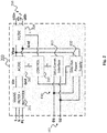
- FIG. 2 shows a schematic view of the bus communication block 100 optionally incorporated in an LED gear 200, according to an embodiment of the present invention.
- the LED gear 200 is designed such that it supplies power to an LED (being connected to the interface 205), and it drives the connected LED.
- the LED gear 200 further includes the mains filter and rectifier unit 201, as it is generally known.
- the LED gear 200 further includes the AC/DC block 202.
- the AC/DC block 202 is configured to be supplied from, for example, a rectified 230VAC mains input and it further provides, for example, a voltage V BUS of 400VDC at its output.
- the LED gear 200 further includes the DC/DC block 204.
- the DC/DC block 204 is optionally configured to be supplied by the 400VDC, and it further delivers either the input voltage for a second (cascaded) DC/DC block, or directly supplies the connected LED with an output voltage/current.
- the LED gear 200 further includes the control circuitry 203.
- the control circuitry 203 may include, for example, a microcontroller and/or Application-Specific Integrated Circuit (ASIC).
- ASIC Application-Specific Integrated Circuit
- the control circuitry 203 controls the AC/DC block 202 and the DC/DC blocks 204 as well as the interface blocks, e.g., as the DALI communication interface 103 and the DALI power supply block 102.
- the module 100 is incorporated in the LED gear 200.
- the module 100 supplies the DALI bus 101, and it communicates via the DALI bus.
- the module 100 may also supply power to an external sensor that is attached to the DALI bus 101.
- the DALI power supply block 102 is supplied by the 400VDC and delivers the DALI bus voltage (e.g., 16VDC) at the output.
- This DALI bus voltage supplies other DALI devices that are connected to the DALI bus 101 (e.g., other LED gears, sensors, etc.).
- the DALI interface logic block 103 that translates between DALI voltage levels and low logic levels (e.g., 0V-3.3V), and it can be evaluated by a microcontroller of the control logic block 203.
- the supply voltage of the internal power supply 102 (i.e., the DALI bus power supply) is used for communication purpose and it does not drive the LEDs (e.g., that are connected to the LED gear interface 205).
- the internal power supply 102 can be switched off, for example, the block 102 is deactivated and the voltage between D+ and D- is 0V.
- the LED gear 200 receives a command to switch-off the internal power supply 102 (e.g., the command may be received via the interface 101).
- the switch A (not shown in FIG. 2 ) is opened, however, the internal power supply block 102 is still activated so the bus voltage is present between D+ and D-.
- the switch A is open, D1 and D2 are not supplied by the internal power supply 102.
- the voltage between D1 and D2 is evaluated using the voltage divider including the R1 and R2 (not shown in FIG. 2 ), as discussed above.
- the switch A when it is determined that the detected bus voltage level is above a threshold value, that means an external power supply is connected to the bus, the switch A remains open and the internal power supply 102 (i.e., the DALI bus power supply block 102) can be deactivated. Hence, the voltage between D+ and D- may go to 0V.
- control circuit 100 is able to prevent a lockout situation.
- FIG. 3 shows a flowchart of the method 300 of a driver circuit for providing a powered interface, according to an embodiment of the present invention.
- the method 300 has a first step 301 of connecting a bus having a non-zero DC voltage level in the quiet state.
- the method 300 has a further step 302 of supplying a connected bus with DC power, wherein the internal power supply is designed such that it can be switched off.
- the method 300 has a further step 303 of controlling the internal power supply, and communicating by receiving and/or sending signals over the bus, and carrying out the following steps upon receipt of a power supply switch-off command:
Landscapes
- Power Sources (AREA)
Abstract
Description
- The present invention relates to a bus interface, and especially to a bus interface which has a local power supply module in order to supply power to a connected bus, especially a bus with a non zero DC voltage level in the quiescent state. An example for such a bus is the DALI bus.
- The bus interface may be part of a bus enabled building technology device, such as e.g. a sensor or a converter for driving lighting means.
- E.g. in the framework of DALI, a central bus power supply is often used. However, there is also the option of replacing such central bus power supply by one or more decentralized bus interfaces with local power supply modules, typically associated with or integrated in a bus enabled building technology device, or preferably a lighting technology device.
- There is the possibility to switch off, via a dedicated command over the bus, the (bus) power supply module of such interface. The inventors have recognized the problem that a lock-out state of the bus may occur in case the last active of such local bus power supply modules in a bus interface is to be switched off.
- It is an object of the present invention to overcome the above-mentioned drawbacks and to provide an improved driver circuit. More specifically, it is an object of the invention to provide a driver circuit and a method, with which a lockout situation in the DALI interface may be prevented.
- This object is achieved by the features of the independent claims. The dependent claims develop further the central idea of the invention. Advantageous features of the present invention are defined in the corresponding dependent claims.
- According to the present invention, the module for providing a powered interface, comprising: at least one terminal configured to connect a bus having a non-zero DC voltage level in the quiet state; an internal power supply configured to supply a connected bus with DC power, wherein the internal power supply is designed such that it can be switched off; and a control circuitry configured to control the internal power supply, and a communication block for receiving and/or sending signals over the bus. The control circuitry is further configured to carry out the following steps upon receipt of an internal power supply switch-off command: switching off the internal power supply and detecting the bus voltage level at a predetermined time after switching off the internal power supply; and continuing the switched-off state of the internal power supply, when it is determined that the detected bus voltage level is above a threshold value; and switching on again the internal power supply and/or sending out a message over the bus, when it is determined that the detected bus voltage level at the predetermined time after switching off drops to the threshold value.
- The internal power supply may be switched on or switched off. Such controlling of the internal power supply advantageously prevents the lockout situation. This approach can also be used for other bus systems, for example, the bus may be based on, a DALI bus, an I2C bus, or a un:q bus (as it is described in the net4more gears specification documents).
- Moreover, the driver circuit may detect a lockout situation in the driver circuity, (e.g., in its DALI interface) and switch on again the power supply and/or send out a message over the bus.
- Preferably, the predetermined time is determined based on the maximum allowed capacitance of the bus.
- Alternatively or in addition, the threshold value for the detected bus voltage is representative of zero.
- Preferably, the control circuitry is based on a digital addressable lighting interface (DALI) communication interface, and the power supply is based on a DALI power supply. For example, in some embodiments, the control circuitry may be or may include the DALI communication interface. The control circuitry may further include, for example, microcontroller and/or Application-Specific Integrated Circuit (ASIC). It may further be configured to control the DALI communication interface, the DALI power supply, etc., without limiting the present disclosure to a specific configuration or a structure.
- According to the present invention, the method of a driver circuit for providing a powered interface, comprises the steps of connecting a bus having a non-zero DC voltage level in the quiet state; supplying a connected bus with DC power, wherein the internal power supply is designed such that it can be switched off; and controlling the internal power supply, and communicating by receiving and/or sending signals over the bus, and carrying out the following steps upon receipt of an internal power supply switch-off command:
- switching off the internal power supply and detecting the bus voltage level at a predetermined time after switching off the internal power supply; and
- continuing the switched-off state of the internal power supply, when it is determined that the detected bus voltage level is above a threshold value; and
- switching on again the internal power supply and/or sending out a message over the bus, when it is determined that the detected bus voltage level at the predetermined time after switching off drops to or below the threshold value.
- Aspects and details of the invention are now explained with reference to the accompanying drawing, wherein:
-
FIG. 1 shows a schematic diagram of a driver circuit according to an embodiment of the present invention, -
FIG. 2 shows a schematic view of the driver circuit for driving a LED load, according to an embodiment of the present invention. -
FIG. 3 shows a flowchart of the method according to an embodiment of the present invention. -
FIG. 1 shows a schematic diagram of adriver circuit 100 for providing a powered interface according to the present invention. -
FIG. 1 shows abus module 100, such as e.g. a DALI bus module which may be part of an actor or sensor in a lighting network. Thebus module 100 comprises aterminal 101 for connection of one or more bus wires, an internal buspower supply block 102, and a bus communication block (interface logic) 103. The buspower supply block 102 is designed to supply the bus connected at 101 with electrical power, such as e.g. a DC voltage level. - The
bus communication block 103 is designed for sending out and/or receiving data over/from the bus connected at 101. - A voltage divider including the resistors R1 and R2 is located between the D1 and D2 lines, near the
terminal 101. The bus voltage level may be measured, for example, by further evaluating the sensed voltage VSNS of the voltage divider, which signal can be sent to a control circuitry (203 inFig. 2 ) of themodule 100. - The
internal power supply 102 supplies a connected bus (e.g., connected to the terminal 101) with DC power. - The
internal power supply 102 is designed such that it can be switched off. For example, theinternal power supply 102 may be adapted such that it can be deactivated. It may also be switched off by using a switch A, and by disconnecting the voltage provided by theinternal power supply 102, without limiting the present disclosure to a specific configuration or a specific procedure for switching off the power supply. - The switch A may be controlled by a signal from the
same control circuitry 203 receiving the VSNS signal indicating the bus voltage level. - Moreover, the "switch-off state" of the
internal power supply 102 is reprehensive of a state in which theinternal power supply 102 is deactivated and/or the voltage between D+ and D- is 0V. - For example, the
internal power supply 102 is an internal DALI power supply. The internal power supply is connected by its D+ line to the D1 line of theterminal 101, and by its D- line to the D2 line of theterminal 101. The switch A is located in the D-line of the internal power supply, without limiting the present disclosure. For example, the switch A may also be located in D+ line of the internal power supply, themodule 100 may have more than one switch, etc. Moreover, the switch A may be used for disconnecting theinternal power supply 102 from the DALI bus, e.g., when a defined command to switch off the internal power supply preferably over the bus is received. - Therefore, the
internal power supply 102 is able to provide the DALI bus with DC power. For example, theinternal power supply 102 provides the DALI bus with a voltage of 16 V at +/- 5% tolerance. - The
internal power supply 102 is designed such that it may be in switch on state, in switch off state, or being switched on again after a switch off state. - In particular, the DALI standards are maintained with such driver circuit. As the invention relates to internal (i.e., local) power supplies for a bus, the problem can arise that the only local bus supply is inadvertently switched off by an internal or external command, resulting in a lockout state.
- The invention solves this problem of the decentralized DALI power supply by performing the following procedure.
- The
control circuitry 203 carries out the following steps upon receipt of an internal power supply switch-off command. This command is preferably received from the connected bus. - The
control circuitry 203 switches off theinternal power supply 102 and detects the bus voltage level at a predetermined time after switching off theinternal power supply 102. This can be a continuous monitoring or the sampling of one or more voltage levels at one or more time steps. Thecontrol circuitry 203 may control the switch A connected to the D- line of the internal power supply, and it may switch off the internal power supply. The control circuitry may detect the bus voltage level by using the voltage divider R1 and R2 which is connected between the D1 and the D2 lines of theterminal 101, and it may further evaluate the sensed voltage VSNS, as discussed above. The bus voltage level is detected at the predetermined time after switching off the internal power supply. - Moreover, the control circuitry may carry our different steps based on the detected bus voltage level.
- For example, the
control circuitry 203 continues the switched-off state of theinternal power supply 102, if it is determined that the detected bus voltage level after a given time period is still at a sufficiently high level, indicating that there is at least one other DC power supply active and connected to the bus. E.g. this can be determined if after a given time period the voltage level on the bus did not fall below a given threshold value. The threshold level is preferably set such that it is within the high-level range of the bus protocol. If thecontrol circuitry 203 determines that there is another power supply connected to the bus, it continues the switch off state of theinternal power supply 102. For example, thecontrol circuitry 203 controls the switch A that is located between the D2 line of thecontrol circuitry 203 and D- line of theinternal power supply 102, to be in the open state, and theinternal power supply 102 can be safely deactivated. - On the other hand, the
control circuitry 203 switches on again theinternal power supply 102 and/or sends out a message over the bus, if it is determined that the detected bus voltage level at the predetermined time after switching off drops below threshold value. This indicates that the presentinternal power supply 102 is currently the only power supply active and connected to the bus. In such a case, thecontrol circuitry 203, for example, controls the switch A that is located between the D2 line of thecontrol circuitry 203 and D- line of theinternal power supply 102, to be in the closed state. The switch A is closed again, and theinternal power supply 102 is not deactivated. In other words, the lockout situation may be prevented. - In such a case, the
communication interface 103 translates between logic levels (e.g., 0 to 3.3 V) that can be sent and received by the microcontroller of the gear, and the DALI bus levels are, for example, in the range of 0 V to 16 V. Theinternal power supply 102 provides the DALI bus with a voltage of, for example, 16 V (the high level can be in the range of 10 V to 22.5 V, according to the DALI standard). - Moreover, the switch A (which can also be in the D+ line) disconnects the
internal power supply 102 from the DALI bus, if the user disables theinternal power supply 102. After the predetermined time, the DALI bus voltage is measured, for example, via a voltage divider R1 and R2, and the sensed voltage VSNS can be evaluated. The predetermined time may depend on the maximum allowed capacitance of the bus. Moreover, if the measured voltage is high (i.e., it is above a threshold value), this means that an external power supply is available in the system. In this case, theinternal power supply 102 can be safely deactivated. - However, if the measured voltage is low (e.g., it is at the threshold value), that means no external power supply is connected to the DALI bus, and the switch A is closed again, and the
internal power supply 102 is not deactivated. In other words, a lock out situation can be prevented. -
FIG. 2 shows a schematic view of thebus communication block 100 optionally incorporated in anLED gear 200, according to an embodiment of the present invention. TheLED gear 200 is designed such that it supplies power to an LED (being connected to the interface 205), and it drives the connected LED. - The
LED gear 200 further includes the mains filter andrectifier unit 201, as it is generally known. TheLED gear 200 further includes the AC/DC block 202. The AC/DC block 202 is configured to be supplied from, for example, a rectified 230VAC mains input and it further provides, for example, a voltage VBUS of 400VDC at its output. - The
LED gear 200 further includes the DC/DC block 204. The DC/DC block 204 is optionally configured to be supplied by the 400VDC, and it further delivers either the input voltage for a second (cascaded) DC/DC block, or directly supplies the connected LED with an output voltage/current. - The
LED gear 200 further includes thecontrol circuitry 203. Thecontrol circuitry 203 may include, for example, a microcontroller and/or Application-Specific Integrated Circuit (ASIC). Thecontrol circuitry 203 controls the AC/DC block 202 and the DC/DC blocks 204 as well as the interface blocks, e.g., as theDALI communication interface 103 and the DALIpower supply block 102. - The
module 100 is incorporated in theLED gear 200. Themodule 100 supplies theDALI bus 101, and it communicates via the DALI bus. Moreover, themodule 100 may also supply power to an external sensor that is attached to theDALI bus 101. - The DALI
power supply block 102 is supplied by the 400VDC and delivers the DALI bus voltage (e.g., 16VDC) at the output. This DALI bus voltage supplies other DALI devices that are connected to the DALI bus 101 (e.g., other LED gears, sensors, etc.). The DALIinterface logic block 103 that translates between DALI voltage levels and low logic levels (e.g., 0V-3.3V), and it can be evaluated by a microcontroller of thecontrol logic block 203. - In the present embodiment, the supply voltage of the internal power supply 102 (i.e., the DALI bus power supply) is used for communication purpose and it does not drive the LEDs (e.g., that are connected to the LED gear interface 205). The
internal power supply 102 can be switched off, for example, theblock 102 is deactivated and the voltage between D+ and D- is 0V. - Moreover, when the
LED gear 200 receives a command to switch-off the internal power supply 102 (e.g., the command may be received via the interface 101). Initially, the switch A (not shown inFIG. 2 ) is opened, however, the internalpower supply block 102 is still activated so the bus voltage is present between D+ and D-. Furthermore, when the switch A is open, D1 and D2 are not supplied by theinternal power supply 102. After the predetermined time, the voltage between D1 and D2 is evaluated using the voltage divider including the R1 and R2 (not shown inFIG. 2 ), as discussed above. - Moreover, when it is determined that the detected bus voltage level is above a threshold value, that means an external power supply is connected to the bus, the switch A remains open and the internal power supply 102 (i.e., the DALI bus power supply block 102) can be deactivated. Hence, the voltage between D+ and D- may go to 0V.
- Furthermore, when it is determined that the detected bus voltage level at the predetermined time after switching off drops to the threshold value (if the voltage is below a certain level), that means no external power supply is connected to the bus. The switch A is being closed again, and therefore, the
internal power supply 102 continues supplying the bus. - Hence, the
control circuit 100 is able to prevent a lockout situation. -
FIG. 3 shows a flowchart of themethod 300 of a driver circuit for providing a powered interface, according to an embodiment of the present invention. - The
method 300 has afirst step 301 of connecting a bus having a non-zero DC voltage level in the quiet state. - The
method 300 has afurther step 302 of supplying a connected bus with DC power, wherein the internal power supply is designed such that it can be switched off. - The
method 300 has afurther step 303 of controlling the internal power supply, and communicating by receiving and/or sending signals over the bus, and carrying out the following steps upon receipt of a power supply switch-off command: - switching off the internal power supply and detecting the bus voltage level at a predetermined time after switching off the internal power supply; and
- continuing the switched-off state of the internal power supply, when it is determined that the detected bus voltage level is above a threshold value; and
- switching on again the internal power supply and/or sending out a message over the bus, when it is determined that the detected bus voltage level at the predetermined time after switching off drops to or below the threshold value.
Claims (5)
- A module (100) for providing a powered interface, comprising:at least one terminal (101) configured to connect a bus having a non-zero DC voltage level in the quiet state;an internal power supply (102) configured to supply a connected bus with DC power, wherein the internal power supply (102) is designed such that it can be switched off;a control circuitry (203) configured to control the internal power supply (102),- a bus communication block (103) for receiving and/or sending signals over the bus, wherein the control circuitry (203) is further configured to carry out the following steps upon receipt of a command for switching-off the internal power supply (102):switching off the internal power supply (102) and detecting the bus voltage level at a predetermined time after switching off the internal power supply (102); andcontinuing the switched-off state of the internal power supply (102), when it is determined that the detected bus voltage level is above a threshold value; andswitching on again the internal power supply (102) and/or sending out a message over the bus, when it is determined that the detected bus voltage level at the predetermined time after switching off drops to or below the threshold value.
- The module (100) according to claim 1, whereinthe predetermined time is determined based on the maximum allowed capacitance of the bus.
- The module (100) according to claim 1 or 2, whereinthe threshold value for the detected bus voltage is representative of zero.
- The module (100) according to claims 1 to 3, whereinbus communication block (103) is based on a digital addressable lighting interface (DALI) communication interface, and the internal power supply (102) is based on an internal DALI power supply.
- A method for operating a module (100) for providing a powered interface, the method (300) comprising the steps of:connecting (301) a bus having a non-zero DC voltage level in the quiet state;supplying (302) a connected bus with DC power, wherein the internal power supply (102) is designed such that it can be switched off; andcontrolling (303) the internal power supply (102), and communicating by receiving and/or sending signals over the bus, and carrying out the following steps upon receipt of an internal power supply switch-off command:switching off the internal power supply (102) and detecting the bus voltage level at a predetermined time after switching off the internal power supply (102); andcontinuing the switched-off state of the internal power supply (102), when it is determined that the detected bus voltage level is above a threshold value; andswitching on again the internal power supply (102) and/or sending out a message over the bus, when it is determined that the detected bus voltage level at the predetermined time after switching off drops to or below the threshold value.
Priority Applications (1)
| Application Number | Priority Date | Filing Date | Title |
|---|---|---|---|
| EP18204500.5A EP3651553B1 (en) | 2018-11-06 | 2018-11-06 | A bus interface and a method for prevention of lockout situation |
Applications Claiming Priority (1)
| Application Number | Priority Date | Filing Date | Title |
|---|---|---|---|
| EP18204500.5A EP3651553B1 (en) | 2018-11-06 | 2018-11-06 | A bus interface and a method for prevention of lockout situation |
Publications (2)
| Publication Number | Publication Date |
|---|---|
| EP3651553A1 true EP3651553A1 (en) | 2020-05-13 |
| EP3651553B1 EP3651553B1 (en) | 2021-09-08 |
Family
ID=64267469
Family Applications (1)
| Application Number | Title | Priority Date | Filing Date |
|---|---|---|---|
| EP18204500.5A Active EP3651553B1 (en) | 2018-11-06 | 2018-11-06 | A bus interface and a method for prevention of lockout situation |
Country Status (1)
| Country | Link |
|---|---|
| EP (1) | EP3651553B1 (en) |
Cited By (1)
| Publication number | Priority date | Publication date | Assignee | Title |
|---|---|---|---|---|
| CN115988707A (en) * | 2022-12-30 | 2023-04-18 | 广州昂宝电子有限公司 | Test circuit for DALI power supply |
Citations (4)
| Publication number | Priority date | Publication date | Assignee | Title |
|---|---|---|---|---|
| EP0749070A2 (en) * | 1995-06-12 | 1996-12-18 | Landis & Gyr Technology Innovation AG | Method for decentralised supply of a bus and apparatus for carrying out the method |
| DE102010042724A1 (en) * | 2010-10-21 | 2012-04-26 | Osram Ag | Device for a lamp application and method for driving the device |
| DE102011056114B3 (en) * | 2011-12-07 | 2012-10-18 | Albrecht Jung Gmbh & Co Kg | Building installation system for supplying power to bus devices e.g. lamp, has bus subscribers that are equipped with power conversion unit, energy storage unit and energy feeding unit |
| DE102016201390A1 (en) * | 2016-01-29 | 2017-08-03 | Tridonic Gmbh & Co Kg | Supply unit for a bus |
-
2018
- 2018-11-06 EP EP18204500.5A patent/EP3651553B1/en active Active
Patent Citations (4)
| Publication number | Priority date | Publication date | Assignee | Title |
|---|---|---|---|---|
| EP0749070A2 (en) * | 1995-06-12 | 1996-12-18 | Landis & Gyr Technology Innovation AG | Method for decentralised supply of a bus and apparatus for carrying out the method |
| DE102010042724A1 (en) * | 2010-10-21 | 2012-04-26 | Osram Ag | Device for a lamp application and method for driving the device |
| DE102011056114B3 (en) * | 2011-12-07 | 2012-10-18 | Albrecht Jung Gmbh & Co Kg | Building installation system for supplying power to bus devices e.g. lamp, has bus subscribers that are equipped with power conversion unit, energy storage unit and energy feeding unit |
| DE102016201390A1 (en) * | 2016-01-29 | 2017-08-03 | Tridonic Gmbh & Co Kg | Supply unit for a bus |
Cited By (1)
| Publication number | Priority date | Publication date | Assignee | Title |
|---|---|---|---|---|
| CN115988707A (en) * | 2022-12-30 | 2023-04-18 | 广州昂宝电子有限公司 | Test circuit for DALI power supply |
Also Published As
| Publication number | Publication date |
|---|---|
| EP3651553B1 (en) | 2021-09-08 |
Similar Documents
| Publication | Publication Date | Title |
|---|---|---|
| US7256556B2 (en) | Equipment and methods for emergency lighting that provides brownout detection and protection | |
| EP2604095B1 (en) | Interface circuit for a lighting device | |
| US8098242B2 (en) | Arrangement comprising a first electronic device and a power supply unit and method for operating an electronic device | |
| CN109728643B (en) | Power receiving device, control method for power receiving device, and storage medium | |
| EP3318004B1 (en) | Power providing device and method, power receiving device | |
| EP3005512B1 (en) | Lps architecture for ups systems | |
| CN108475942B (en) | Emergency unit, lighting system, emergency operating device and emergency unit operating method | |
| US12120797B2 (en) | Power supply device, a power receiving device and power supply and receipt methods | |
| US20090243565A1 (en) | Method and apparatus for detecting end of start up phase | |
| US8531058B2 (en) | Electrical appliance | |
| EP4456673A1 (en) | Interface control circuit, control method and interface control device | |
| EP3651553B1 (en) | A bus interface and a method for prevention of lockout situation | |
| EP0897562B1 (en) | Video display unit | |
| US10852755B2 (en) | HVAC signaling over a two-wire connection | |
| US20060139834A1 (en) | System and method for automatically detecting power supply voltage | |
| US6535405B2 (en) | Power supply device having two AC power inputs | |
| EP3888422B1 (en) | Power supply for an led lighting unit | |
| TWM523235U (en) | Voltage converter | |
| US20040037019A1 (en) | Power supply control circuit | |
| US6815844B2 (en) | Circuit for supplying power to a network termination unit of a message transmission system | |
| CN205177357U (en) | Prevent power failure lamp house | |
| EP4432785B1 (en) | Power-line communication emergency lighting fixture | |
| KR101930289B1 (en) | Power control apparatus | |
| CN220732417U (en) | Elevator power supply device and elevator | |
| EP4635260A1 (en) | A lamp driving apparatus and a led lamp |
Legal Events
| Date | Code | Title | Description |
|---|---|---|---|
| PUAI | Public reference made under article 153(3) epc to a published international application that has entered the european phase |
Free format text: ORIGINAL CODE: 0009012 |
|
| STAA | Information on the status of an ep patent application or granted ep patent |
Free format text: STATUS: THE APPLICATION HAS BEEN PUBLISHED |
|
| AK | Designated contracting states |
Kind code of ref document: A1 Designated state(s): AL AT BE BG CH CY CZ DE DK EE ES FI FR GB GR HR HU IE IS IT LI LT LU LV MC MK MT NL NO PL PT RO RS SE SI SK SM TR |
|
| AX | Request for extension of the european patent |
Extension state: BA ME |
|
| STAA | Information on the status of an ep patent application or granted ep patent |
Free format text: STATUS: REQUEST FOR EXAMINATION WAS MADE |
|
| 17P | Request for examination filed |
Effective date: 20200721 |
|
| RBV | Designated contracting states (corrected) |
Designated state(s): AL AT BE BG CH CY CZ DE DK EE ES FI FR GB GR HR HU IE IS IT LI LT LU LV MC MK MT NL NO PL PT RO RS SE SI SK SM TR |
|
| REG | Reference to a national code |
Ref country code: DE Ref legal event code: R079 Ref document number: 602018023170 Country of ref document: DE Free format text: PREVIOUS MAIN CLASS: H05B0037020000 Ipc: H05B0047180000 |
|
| RIC1 | Information provided on ipc code assigned before grant |
Ipc: H05B 47/18 20200101AFI20210324BHEP |
|
| GRAP | Despatch of communication of intention to grant a patent |
Free format text: ORIGINAL CODE: EPIDOSNIGR1 |
|
| STAA | Information on the status of an ep patent application or granted ep patent |
Free format text: STATUS: GRANT OF PATENT IS INTENDED |
|
| INTG | Intention to grant announced |
Effective date: 20210610 |
|
| GRAS | Grant fee paid |
Free format text: ORIGINAL CODE: EPIDOSNIGR3 |
|
| GRAA | (expected) grant |
Free format text: ORIGINAL CODE: 0009210 |
|
| STAA | Information on the status of an ep patent application or granted ep patent |
Free format text: STATUS: THE PATENT HAS BEEN GRANTED |
|
| AK | Designated contracting states |
Kind code of ref document: B1 Designated state(s): AL AT BE BG CH CY CZ DE DK EE ES FI FR GB GR HR HU IE IS IT LI LT LU LV MC MK MT NL NO PL PT RO RS SE SI SK SM TR |
|
| REG | Reference to a national code |
Ref country code: GB Ref legal event code: FG4D |
|
| REG | Reference to a national code |
Ref country code: CH Ref legal event code: EP Ref country code: AT Ref legal event code: REF Ref document number: 1429762 Country of ref document: AT Kind code of ref document: T Effective date: 20210915 |
|
| REG | Reference to a national code |
Ref country code: DE Ref legal event code: R096 Ref document number: 602018023170 Country of ref document: DE |
|
| REG | Reference to a national code |
Ref country code: IE Ref legal event code: FG4D |
|
| REG | Reference to a national code |
Ref country code: LT Ref legal event code: MG9D |
|
| REG | Reference to a national code |
Ref country code: NL Ref legal event code: MP Effective date: 20210908 |
|
| PG25 | Lapsed in a contracting state [announced via postgrant information from national office to epo] |
Ref country code: SE Free format text: LAPSE BECAUSE OF FAILURE TO SUBMIT A TRANSLATION OF THE DESCRIPTION OR TO PAY THE FEE WITHIN THE PRESCRIBED TIME-LIMIT Effective date: 20210908 Ref country code: RS Free format text: LAPSE BECAUSE OF FAILURE TO SUBMIT A TRANSLATION OF THE DESCRIPTION OR TO PAY THE FEE WITHIN THE PRESCRIBED TIME-LIMIT Effective date: 20210908 Ref country code: HR Free format text: LAPSE BECAUSE OF FAILURE TO SUBMIT A TRANSLATION OF THE DESCRIPTION OR TO PAY THE FEE WITHIN THE PRESCRIBED TIME-LIMIT Effective date: 20210908 Ref country code: FI Free format text: LAPSE BECAUSE OF FAILURE TO SUBMIT A TRANSLATION OF THE DESCRIPTION OR TO PAY THE FEE WITHIN THE PRESCRIBED TIME-LIMIT Effective date: 20210908 Ref country code: ES Free format text: LAPSE BECAUSE OF FAILURE TO SUBMIT A TRANSLATION OF THE DESCRIPTION OR TO PAY THE FEE WITHIN THE PRESCRIBED TIME-LIMIT Effective date: 20210908 Ref country code: BG Free format text: LAPSE BECAUSE OF FAILURE TO SUBMIT A TRANSLATION OF THE DESCRIPTION OR TO PAY THE FEE WITHIN THE PRESCRIBED TIME-LIMIT Effective date: 20211208 Ref country code: LT Free format text: LAPSE BECAUSE OF FAILURE TO SUBMIT A TRANSLATION OF THE DESCRIPTION OR TO PAY THE FEE WITHIN THE PRESCRIBED TIME-LIMIT Effective date: 20210908 Ref country code: NO Free format text: LAPSE BECAUSE OF FAILURE TO SUBMIT A TRANSLATION OF THE DESCRIPTION OR TO PAY THE FEE WITHIN THE PRESCRIBED TIME-LIMIT Effective date: 20211208 |
|
| PG25 | Lapsed in a contracting state [announced via postgrant information from national office to epo] |
Ref country code: LV Free format text: LAPSE BECAUSE OF FAILURE TO SUBMIT A TRANSLATION OF THE DESCRIPTION OR TO PAY THE FEE WITHIN THE PRESCRIBED TIME-LIMIT Effective date: 20210908 Ref country code: GR Free format text: LAPSE BECAUSE OF FAILURE TO SUBMIT A TRANSLATION OF THE DESCRIPTION OR TO PAY THE FEE WITHIN THE PRESCRIBED TIME-LIMIT Effective date: 20211209 |
|
| PG25 | Lapsed in a contracting state [announced via postgrant information from national office to epo] |
Ref country code: IS Free format text: LAPSE BECAUSE OF FAILURE TO SUBMIT A TRANSLATION OF THE DESCRIPTION OR TO PAY THE FEE WITHIN THE PRESCRIBED TIME-LIMIT Effective date: 20220108 Ref country code: PT Free format text: LAPSE BECAUSE OF FAILURE TO SUBMIT A TRANSLATION OF THE DESCRIPTION OR TO PAY THE FEE WITHIN THE PRESCRIBED TIME-LIMIT Effective date: 20220110 Ref country code: PL Free format text: LAPSE BECAUSE OF FAILURE TO SUBMIT A TRANSLATION OF THE DESCRIPTION OR TO PAY THE FEE WITHIN THE PRESCRIBED TIME-LIMIT Effective date: 20210908 Ref country code: NL Free format text: LAPSE BECAUSE OF FAILURE TO SUBMIT A TRANSLATION OF THE DESCRIPTION OR TO PAY THE FEE WITHIN THE PRESCRIBED TIME-LIMIT Effective date: 20210908 Ref country code: EE Free format text: LAPSE BECAUSE OF FAILURE TO SUBMIT A TRANSLATION OF THE DESCRIPTION OR TO PAY THE FEE WITHIN THE PRESCRIBED TIME-LIMIT Effective date: 20210908 Ref country code: CZ Free format text: LAPSE BECAUSE OF FAILURE TO SUBMIT A TRANSLATION OF THE DESCRIPTION OR TO PAY THE FEE WITHIN THE PRESCRIBED TIME-LIMIT Effective date: 20210908 Ref country code: AL Free format text: LAPSE BECAUSE OF FAILURE TO SUBMIT A TRANSLATION OF THE DESCRIPTION OR TO PAY THE FEE WITHIN THE PRESCRIBED TIME-LIMIT Effective date: 20210908 Ref country code: SM Free format text: LAPSE BECAUSE OF FAILURE TO SUBMIT A TRANSLATION OF THE DESCRIPTION OR TO PAY THE FEE WITHIN THE PRESCRIBED TIME-LIMIT Effective date: 20210908 Ref country code: SK Free format text: LAPSE BECAUSE OF FAILURE TO SUBMIT A TRANSLATION OF THE DESCRIPTION OR TO PAY THE FEE WITHIN THE PRESCRIBED TIME-LIMIT Effective date: 20210908 Ref country code: RO Free format text: LAPSE BECAUSE OF FAILURE TO SUBMIT A TRANSLATION OF THE DESCRIPTION OR TO PAY THE FEE WITHIN THE PRESCRIBED TIME-LIMIT Effective date: 20210908 |
|
| REG | Reference to a national code |
Ref country code: DE Ref legal event code: R097 Ref document number: 602018023170 Country of ref document: DE |
|
| PG25 | Lapsed in a contracting state [announced via postgrant information from national office to epo] |
Ref country code: MC Free format text: LAPSE BECAUSE OF FAILURE TO SUBMIT A TRANSLATION OF THE DESCRIPTION OR TO PAY THE FEE WITHIN THE PRESCRIBED TIME-LIMIT Effective date: 20210908 |
|
| REG | Reference to a national code |
Ref country code: CH Ref legal event code: PL |
|
| PLBE | No opposition filed within time limit |
Free format text: ORIGINAL CODE: 0009261 |
|
| STAA | Information on the status of an ep patent application or granted ep patent |
Free format text: STATUS: NO OPPOSITION FILED WITHIN TIME LIMIT |
|
| PG25 | Lapsed in a contracting state [announced via postgrant information from national office to epo] |
Ref country code: LU Free format text: LAPSE BECAUSE OF NON-PAYMENT OF DUE FEES Effective date: 20211106 Ref country code: DK Free format text: LAPSE BECAUSE OF FAILURE TO SUBMIT A TRANSLATION OF THE DESCRIPTION OR TO PAY THE FEE WITHIN THE PRESCRIBED TIME-LIMIT Effective date: 20210908 Ref country code: BE Free format text: LAPSE BECAUSE OF NON-PAYMENT OF DUE FEES Effective date: 20211130 |
|
| REG | Reference to a national code |
Ref country code: BE Ref legal event code: MM Effective date: 20211130 |
|
| 26N | No opposition filed |
Effective date: 20220609 |
|
| PG25 | Lapsed in a contracting state [announced via postgrant information from national office to epo] |
Ref country code: SI Free format text: LAPSE BECAUSE OF FAILURE TO SUBMIT A TRANSLATION OF THE DESCRIPTION OR TO PAY THE FEE WITHIN THE PRESCRIBED TIME-LIMIT Effective date: 20210908 Ref country code: LI Free format text: LAPSE BECAUSE OF NON-PAYMENT OF DUE FEES Effective date: 20211130 Ref country code: CH Free format text: LAPSE BECAUSE OF NON-PAYMENT OF DUE FEES Effective date: 20211130 |
|
| PG25 | Lapsed in a contracting state [announced via postgrant information from national office to epo] |
Ref country code: IE Free format text: LAPSE BECAUSE OF NON-PAYMENT OF DUE FEES Effective date: 20211106 |
|
| PG25 | Lapsed in a contracting state [announced via postgrant information from national office to epo] |
Ref country code: IT Free format text: LAPSE BECAUSE OF FAILURE TO SUBMIT A TRANSLATION OF THE DESCRIPTION OR TO PAY THE FEE WITHIN THE PRESCRIBED TIME-LIMIT Effective date: 20210908 |
|
| PG25 | Lapsed in a contracting state [announced via postgrant information from national office to epo] |
Ref country code: CY Free format text: LAPSE BECAUSE OF FAILURE TO SUBMIT A TRANSLATION OF THE DESCRIPTION OR TO PAY THE FEE WITHIN THE PRESCRIBED TIME-LIMIT Effective date: 20210908 |
|
| P01 | Opt-out of the competence of the unified patent court (upc) registered |
Effective date: 20230530 |
|
| PG25 | Lapsed in a contracting state [announced via postgrant information from national office to epo] |
Ref country code: HU Free format text: LAPSE BECAUSE OF FAILURE TO SUBMIT A TRANSLATION OF THE DESCRIPTION OR TO PAY THE FEE WITHIN THE PRESCRIBED TIME-LIMIT; INVALID AB INITIO Effective date: 20181106 |
|
| PG25 | Lapsed in a contracting state [announced via postgrant information from national office to epo] |
Ref country code: MK Free format text: LAPSE BECAUSE OF FAILURE TO SUBMIT A TRANSLATION OF THE DESCRIPTION OR TO PAY THE FEE WITHIN THE PRESCRIBED TIME-LIMIT Effective date: 20210908 |
|
| PG25 | Lapsed in a contracting state [announced via postgrant information from national office to epo] |
Ref country code: TR Free format text: LAPSE BECAUSE OF FAILURE TO SUBMIT A TRANSLATION OF THE DESCRIPTION OR TO PAY THE FEE WITHIN THE PRESCRIBED TIME-LIMIT Effective date: 20210908 |
|
| PG25 | Lapsed in a contracting state [announced via postgrant information from national office to epo] |
Ref country code: MT Free format text: LAPSE BECAUSE OF FAILURE TO SUBMIT A TRANSLATION OF THE DESCRIPTION OR TO PAY THE FEE WITHIN THE PRESCRIBED TIME-LIMIT Effective date: 20210908 |
|
| REG | Reference to a national code |
Ref country code: AT Ref legal event code: MM01 Ref document number: 1429762 Country of ref document: AT Kind code of ref document: T Effective date: 20231106 |
|
| PG25 | Lapsed in a contracting state [announced via postgrant information from national office to epo] |
Ref country code: AT Free format text: LAPSE BECAUSE OF NON-PAYMENT OF DUE FEES Effective date: 20231106 |
|
| PG25 | Lapsed in a contracting state [announced via postgrant information from national office to epo] |
Ref country code: AT Free format text: LAPSE BECAUSE OF NON-PAYMENT OF DUE FEES Effective date: 20231106 |
|
| REG | Reference to a national code |
Ref country code: AT Ref legal event code: UEP Ref document number: 1429762 Country of ref document: AT Kind code of ref document: T Effective date: 20210908 |
|
| REG | Reference to a national code |
Ref country code: DE Ref legal event code: R084 Ref document number: 602018023170 Country of ref document: DE |
|
| PGFP | Annual fee paid to national office [announced via postgrant information from national office to epo] |
Ref country code: DE Payment date: 20251126 Year of fee payment: 8 |
|
| PGFP | Annual fee paid to national office [announced via postgrant information from national office to epo] |
Ref country code: GB Payment date: 20251125 Year of fee payment: 8 |
|
| PGFP | Annual fee paid to national office [announced via postgrant information from national office to epo] |
Ref country code: FR Payment date: 20251124 Year of fee payment: 8 |
|
| PGFP | Annual fee paid to national office [announced via postgrant information from national office to epo] |
Ref country code: AT Payment date: 20260410 Year of fee payment: 5 |