EP3651351A1 - Power conversion device and electric power steering device - Google Patents
Power conversion device and electric power steering device Download PDFInfo
- Publication number
- EP3651351A1 EP3651351A1 EP17916934.7A EP17916934A EP3651351A1 EP 3651351 A1 EP3651351 A1 EP 3651351A1 EP 17916934 A EP17916934 A EP 17916934A EP 3651351 A1 EP3651351 A1 EP 3651351A1
- Authority
- EP
- European Patent Office
- Prior art keywords
- voltage
- phase
- phase inverter
- average
- ref
- Prior art date
- Legal status (The legal status is an assumption and is not a legal conclusion. Google has not performed a legal analysis and makes no representation as to the accuracy of the status listed.)
- Granted
Links
Images





Classifications
-
- H—ELECTRICITY
- H02—GENERATION; CONVERSION OR DISTRIBUTION OF ELECTRIC POWER
- H02P—CONTROL OR REGULATION OF ELECTRIC MOTORS, ELECTRIC GENERATORS OR DYNAMO-ELECTRIC CONVERTERS; CONTROLLING TRANSFORMERS, REACTORS OR CHOKE COILS
- H02P25/00—Arrangements or methods for the control of AC motors characterised by the kind of AC motor or by structural details
- H02P25/16—Arrangements or methods for the control of AC motors characterised by the kind of AC motor or by structural details characterised by the circuit arrangement or by the kind of wiring
- H02P25/22—Multiple windings; Windings for more than three phases
-
- B—PERFORMING OPERATIONS; TRANSPORTING
- B62—LAND VEHICLES FOR TRAVELLING OTHERWISE THAN ON RAILS
- B62D—MOTOR VEHICLES; TRAILERS
- B62D5/00—Power-assisted or power-driven steering
- B62D5/04—Power-assisted or power-driven steering electrical, e.g. using an electric servo-motor connected to, or forming part of, the steering gear
- B62D5/0457—Power-assisted or power-driven steering electrical, e.g. using an electric servo-motor connected to, or forming part of, the steering gear characterised by control features of the drive means as such
- B62D5/046—Controlling the motor
-
- H—ELECTRICITY
- H02—GENERATION; CONVERSION OR DISTRIBUTION OF ELECTRIC POWER
- H02M—APPARATUS FOR CONVERSION BETWEEN AC AND AC, BETWEEN AC AND DC, OR BETWEEN DC AND DC, AND FOR USE WITH MAINS OR SIMILAR POWER SUPPLY SYSTEMS; CONVERSION OF DC OR AC INPUT POWER INTO SURGE OUTPUT POWER; CONTROL OR REGULATION THEREOF
- H02M7/00—Conversion of AC power input into DC power output; Conversion of DC power input into AC power output
- H02M7/42—Conversion of DC power input into AC power output without possibility of reversal
- H02M7/44—Conversion of DC power input into AC power output without possibility of reversal by static converters
- H02M7/48—Conversion of DC power input into AC power output without possibility of reversal by static converters using discharge tubes with control electrode or semiconductor devices with control electrode
- H02M7/493—Conversion of DC power input into AC power output without possibility of reversal by static converters using discharge tubes with control electrode or semiconductor devices with control electrode the static converters being arranged for operation in parallel
-
- H—ELECTRICITY
- H02—GENERATION; CONVERSION OR DISTRIBUTION OF ELECTRIC POWER
- H02M—APPARATUS FOR CONVERSION BETWEEN AC AND AC, BETWEEN AC AND DC, OR BETWEEN DC AND DC, AND FOR USE WITH MAINS OR SIMILAR POWER SUPPLY SYSTEMS; CONVERSION OF DC OR AC INPUT POWER INTO SURGE OUTPUT POWER; CONTROL OR REGULATION THEREOF
- H02M7/00—Conversion of AC power input into DC power output; Conversion of DC power input into AC power output
- H02M7/42—Conversion of DC power input into AC power output without possibility of reversal
- H02M7/44—Conversion of DC power input into AC power output without possibility of reversal by static converters
- H02M7/48—Conversion of DC power input into AC power output without possibility of reversal by static converters using discharge tubes with control electrode or semiconductor devices with control electrode
- H02M7/53—Conversion of DC power input into AC power output without possibility of reversal by static converters using discharge tubes with control electrode or semiconductor devices with control electrode using devices of a triode or transistor type requiring continuous application of a control signal
- H02M7/537—Conversion of DC power input into AC power output without possibility of reversal by static converters using discharge tubes with control electrode or semiconductor devices with control electrode using devices of a triode or transistor type requiring continuous application of a control signal using semiconductor devices only, e.g. single switched pulse inverters
- H02M7/5387—Conversion of DC power input into AC power output without possibility of reversal by static converters using discharge tubes with control electrode or semiconductor devices with control electrode using devices of a triode or transistor type requiring continuous application of a control signal using semiconductor devices only, e.g. single switched pulse inverters in a bridge configuration
-
- H—ELECTRICITY
- H02—GENERATION; CONVERSION OR DISTRIBUTION OF ELECTRIC POWER
- H02M—APPARATUS FOR CONVERSION BETWEEN AC AND AC, BETWEEN AC AND DC, OR BETWEEN DC AND DC, AND FOR USE WITH MAINS OR SIMILAR POWER SUPPLY SYSTEMS; CONVERSION OF DC OR AC INPUT POWER INTO SURGE OUTPUT POWER; CONTROL OR REGULATION THEREOF
- H02M7/00—Conversion of AC power input into DC power output; Conversion of DC power input into AC power output
- H02M7/42—Conversion of DC power input into AC power output without possibility of reversal
- H02M7/44—Conversion of DC power input into AC power output without possibility of reversal by static converters
- H02M7/48—Conversion of DC power input into AC power output without possibility of reversal by static converters using discharge tubes with control electrode or semiconductor devices with control electrode
- H02M7/53—Conversion of DC power input into AC power output without possibility of reversal by static converters using discharge tubes with control electrode or semiconductor devices with control electrode using devices of a triode or transistor type requiring continuous application of a control signal
- H02M7/537—Conversion of DC power input into AC power output without possibility of reversal by static converters using discharge tubes with control electrode or semiconductor devices with control electrode using devices of a triode or transistor type requiring continuous application of a control signal using semiconductor devices only, e.g. single switched pulse inverters
- H02M7/5387—Conversion of DC power input into AC power output without possibility of reversal by static converters using discharge tubes with control electrode or semiconductor devices with control electrode using devices of a triode or transistor type requiring continuous application of a control signal using semiconductor devices only, e.g. single switched pulse inverters in a bridge configuration
- H02M7/53871—Conversion of DC power input into AC power output without possibility of reversal by static converters using discharge tubes with control electrode or semiconductor devices with control electrode using devices of a triode or transistor type requiring continuous application of a control signal using semiconductor devices only, e.g. single switched pulse inverters in a bridge configuration with automatic control of output voltage or current
-
- H—ELECTRICITY
- H02—GENERATION; CONVERSION OR DISTRIBUTION OF ELECTRIC POWER
- H02P—CONTROL OR REGULATION OF ELECTRIC MOTORS, ELECTRIC GENERATORS OR DYNAMO-ELECTRIC CONVERTERS; CONTROLLING TRANSFORMERS, REACTORS OR CHOKE COILS
- H02P27/00—Arrangements or methods for the control of AC motors characterised by the kind of supply voltage
- H02P27/04—Arrangements or methods for the control of AC motors characterised by the kind of supply voltage using variable-frequency supply voltage, e.g. inverter or converter supply voltage
- H02P27/06—Arrangements or methods for the control of AC motors characterised by the kind of supply voltage using variable-frequency supply voltage, e.g. inverter or converter supply voltage using DC to AC converters or inverters
- H02P27/08—Arrangements or methods for the control of AC motors characterised by the kind of supply voltage using variable-frequency supply voltage, e.g. inverter or converter supply voltage using DC to AC converters or inverters with pulse width modulation
-
- H—ELECTRICITY
- H02—GENERATION; CONVERSION OR DISTRIBUTION OF ELECTRIC POWER
- H02P—CONTROL OR REGULATION OF ELECTRIC MOTORS, ELECTRIC GENERATORS OR DYNAMO-ELECTRIC CONVERTERS; CONTROLLING TRANSFORMERS, REACTORS OR CHOKE COILS
- H02P2207/00—Indexing scheme relating to controlling arrangements characterised by the type of motor
- H02P2207/07—Doubly fed machines receiving two supplies both on the stator only wherein the power supply is fed to different sets of stator windings or to rotor and stator windings
Definitions
- the present invention relates to a power conversion device and an electric power steering apparatus.
- the motor control apparatus includes: a plurality of power converters; a plurality of motor command calculation units; and a plurality of carrier generation units, which are provided in association with a plurality of motors, respectively, in which the plurality of carrier generation units are each configured to generate a plurality of carrier signals, and a carrier frequency control unit is configured to control frequencies of the plurality of carrier signals so that the frequencies of the plurality of carrier signals fluctuate within a plurality of preset frequency ranges which are defined for each of the plurality of carrier signals. Further, the plurality of preset frequency ranges are determined in advance not to overlap one another, to thereby reduce noise generated by switching operations of the power converters (see Patent Literature 1).
- the power conversion device includes two inverters, in which a "flatbed two-phase modulation" is executed in one inverter unit, to subtract from all voltage command signals of three phases a value obtained by subtracting a preset lower limit value from the smallest voltage command signal among the voltage command signals of the three phases so that the smallest voltage command signal equals the preset lower limit value, and a "flattop two-phase modulation process" is executed in another inverter unit, to subtract from all voltage command signals of three phases a value obtained by subtracting a preset upper limit value from the largest voltage command signal among the voltage command signals of the three phases so that the largest voltage command signal equals the preset upper limit value.
- Patent Literature 1 With the method described in Patent Literature 1, in which a plurality of frequencies are set as a frequency of a pulse width modulation (PWM) carrier wave for respective inverters, and one of the frequencies is changed to be selected, it is required to store a plurality of PWM carrier waves and thus prepare a large memory capacity. Consequently, a control apparatus cannot be easily mounted to an inexpensive microcontroller (CPU).
- PWM pulse width modulation
- the present invention has been made to solve the above-mentioned problems, and an object of the present invention is generally to provide an electric power steering apparatus and a power conversion device including two multi-phase inverters, which can suppress noise within a frequency band defined by noise regulation without changing a frequency of a PWM carrier wave of each inverter.
- a power conversion device and the like including: a first multi-phase inverter and a second multi-phase inverter, which are configured to receive a DC voltage output from a DC power supply, and execute power conversion to convert the DC voltage into AC voltages and then output the resultant AC voltages; a drive voltage command calculation unit configured to calculate first multi-phase drive voltage commands and second multi-phase drive voltage commands, which cause the first multi-phase inverter and the second multi-phase inverter to drive a load based on an external control command; a first average voltage adjustment unit configured to output, as first multi-phase voltage commands, values obtained by adjusting the first multi-phase drive voltage commands with use of a first offset voltage, to thereby control the first multi-phase inverter; a second average voltage adjustment unit configured to output, as second multi-phase voltage commands, values obtained by adjusting the second multi-phase drive voltage commands with use of a second offset voltage, to thereby control the second multi-phase inverter; and a voltage adjustment control unit
- the electric power steering apparatus and the power conversion device including two multi-phase inverters, which can suppress noise within a frequency band defined by noise regulation without changing a frequency of a PWM carrier wave of each inverter.
- an absolute value (Vave_dif_abs) of a differential voltage (Vave_dif) being a difference between a first average voltage (Vave1) and a second average voltage (Vave2) is set equal to or less than a value derived from Expression (1), the first average voltage (Vave1) being an average value of first voltage commands (Vu1_ref, Vv1_ref', and Vw1_ref') of respective phases and the second average voltage (Vave2) being an average value of second voltage commands (Vu2_ref', Vv2_ref', and Vw2_ref') of respective phases, the first and second voltage commands being command values for AC voltages to be output from a first multi-phase inverter and a second multi-phase inverter of a power conversion device, respectively: k 2 ⁇ fc / fr ⁇ Vdc V where
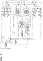
- FIG. 1 is a diagram for illustrating an overall configuration of a power conversion device according to a first embodiment of the present invention.
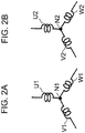
- An AC rotating machine 1 includes two sets of three-phase windings, that is, first three-phase windings U1, V1, and W1, and second three-phase windings U2, V2, and W2. As illustrated in FIG. 2A and FIG. 2B , in the AC rotating machine 1, the first three-phase windings U1-V1-W1 of FIG. 2A and the second three-phase windings U2-V2-W2 of FIG. 2B are arranged in phase in terms of an electric angle, and neutral points N1 and N2 thereof are not electrically connected.
- a DC power supply 2 is configured to output a DC voltage Vdc to a first three-phase inverter 3a and a second three-phase inverter 3b.
- the DC power supply 2 includes all devices that can output a DC voltage, such as a battery, a DC-DC converter, a diode rectifier, or a PWM rectifier.
- the DC power supply 2 has a positive-side potential Vp and a negative-side potential Vn.
- the first three-phase inverter 3a is configured to execute PWM modulation through comparison with a PWM carrier wave having a frequency fc based on first three-phase voltage commands Vu1_ref', Vv1_ref', and Vw1_ref' as described later, so as to perform inverse conversion, that is, DC-AC conversion of the DC voltage Vdc received from the DC power supply 2, to thereby apply resultant AC voltages Vu1, Vv1, and Vw1 to the first three-phase windings U1, V1, and W1 of the AC rotating machine 1.
- Switches Sup1 to Swp1, and switches Sun1 to Swn1 are prepared by connecting, in inverse parallel, diodes and semiconductor switches that are any ones of IGBTs, bipolar transistors, MOS power transistors, and the like.
- the second three-phase inverter 3b is configured to execute PWM modulation through comparison with a PWM carrier wave having a frequency fc based on second three-phase voltage commands Vu2_ref', Vv2_ref', and Vw2_ref' as described later, so as to perform inverse conversion, that is, DC-AC conversion of the DC voltage Vdc received from the DC power supply 2, to thereby apply resultant AC voltages Vu2, Vv2, and Vw2 to the second three-phase windings U2, V2, and W2 of the AC rotating machine 1.
- Switches Sup2 to Swp2, and switches Sun2 to Swn2 are prepared by connecting, in inverse parallel, diodes and semiconductor switches that are any ones of IGBTs, bipolar transistors, MOS power transistors, and the like.
- a drive voltage command calculation unit 4a is configured to calculate first three-phase drive voltage commands Vu1_ref, Vv1_ref, and Vw1_ref and second three-phase drive voltage commands Vu2_ref, Vv2_ref, and Vw2_ref used to drive the AC rotating machine 1 in accordance with a control command CCO.
- the first three-phase drive voltage commands Vu1_ref, Vv1_ref, and Vw1_ref and the second three-phase drive voltage commands Vu2_ref, Vv2_ref, and Vw2_ref are calculated based on publicly-known technologies as described below.
- V/F control executed to determine amplitudes of the first three-phase drive voltage commands and the second three-phase drive voltage commands under a state in which a speed command or a frequency command f for the AC rotating machine 1 is set as the control command CCO of FIG. 1 .
- Another example is current feedback control, in which a current command for the AC rotating machine 1 is set as the control command CCO, and the first three-phase drive voltage commands Vu1_ref, Vv1_ref, and Vw1_ref are calculated through proportional-integral control so as to reduce to zero a deviation between the current command and values of currents flowing through the first three-phase windings U1, V1, and W1, and the second three-phase drive voltage commands Vu2_ref, Vv2_ref, and Vw2_ref are calculated through proportional-integral control so as to reduce to zero a deviation between the current command and values of currents flowing through the second three-phase windings U2, V2, and W2.
- a first average voltage adjustment unit 5a is configured to uniformly add a first offset voltage Voffset1 to the first three-phase drive voltage commands Vu1_ref, Vv1_ref, and Vw1_ref output from the drive voltage command calculation unit 4a, and then output the resultant commands as the first three-phase voltage commands Vu1_ref', Vv1_ref', and Vw1_ref'.
- a first average voltage Vave1 as an average voltage of the first three-phase voltage commands Vu1_ref', Vv1_ref', and Vw1_ref' can be adjusted through adjustment of the first offset voltage Voffset1. This adjustment is described below.
- the first three-phase drive voltage commands Vu1_ref, Vv1_ref, and Vw1_ref can be derived from Expressions (1-1) to (1-3) as three-phase AC voltages.
- Vamp1 represents an amplitude of the respective first three-phase drive voltage commands
- ⁇ v1 represents a phase of the respective first three-phase drive voltage commands.
- Vu 1 _ ref Vamp 1 ⁇ sin ⁇ v 1
- Vv 1 _ ref Vamp 1 ⁇ sin ⁇ v 1 ⁇ 2 ⁇ / 3
- Vw 1 _ ref Vamp 1 ⁇ sin ⁇ v 1 + 2 ⁇ / 3
- the first three-phase voltage commands Vu1_ref', Vv1_ref', and Vw1_ref' are obtained by adding the first offset voltage Voffset1 to the first three-phase drive voltage commands Vu1_ref, Vv1_ref, and Vw1_ref, and thus those commands are represented by Expressions (1-4) to (1-6).
- the first average voltage Vave1 equals the first offset voltage Voffset1, and thus the first average voltage Vave1 can be adjusted through the adjustment of the first offset voltage Voffset1.
- a second average voltage adjustment unit 5b is configured to uniformly add a second offset voltage Voffset2 to the second three-phase drive voltage commands Vu2_ref, Vv2_ref, and Vw2_ref output from the drive voltage command calculation unit 4a, and then output the resultant commands as the second three-phase voltage commands Vu2_ref', Vv2_ref', and Vw2_ref'.
- a second average voltage Vave2 as an average voltage of the second three-phase voltage commands Vu2_ref', Vv2_ref', and Vw2_ref' can be adjusted through adjustment of the second offset voltage Voffset2. This adjustment is described below.
- the second three-phase drive voltage commands Vu2_ref, Vv2_ref, and Vw2_ref can be derived from Expressions (1-8) to (1-10) as three-phase AC voltages.
- Vamp2 represents an amplitude of the respective second three-phase drive voltage commands
- ⁇ v2 represents a phase of the respective second three-phase drive voltage commands.
- Vu 2 _ ref Vamp 2 ⁇ sin ⁇ v 2
- Vv 2 _ ref Vamp 2 ⁇ sin ⁇ v 2 ⁇ 2 ⁇ / 3
- Vw 2 _ ref Vamp 2 ⁇ sin ⁇ v 2 + 2 ⁇ / 3
- the second three-phase voltage commands Vu2_ref', Vv2_ref', and Vw2_ref' are obtained by adding the second offset voltage Voffset2 to the second three-phase drive voltage commands Vu2_ref, Vv2_ref, and Vw2_ref, and thus those commands are represented by Expressions (1-11) to (1-13).
- the second average voltage Vave2 equals the second offset voltage Voffset2, and thus the second average voltage Vave2 can be adjusted through the adjustment of the second offset voltage Voffset2.
- FIG. 3 is a chart for showing how to generate the AC voltages Vu1, Vv1, and Vw1 in the first embodiment of the present invention.
- FIG. 3 operations of the switches Sup1, Svp1, and Swp1 on the positive side of the first three-phase inverter 3a are illustrated, and operations of the switches Sun1, Svn1, and Swn1, which operate inversely to the operations of the switches on the positive side, are not illustrated.
- the AC voltages Vu1, Vv1, and Vw1 output from the first three-phase inverter 3a are PWM voltages with the cycle Tc, that is, the frequency fc.
- the frequency thereof also matches the frequency fc of the PWM carrier wave PWMC.
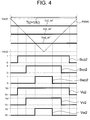
- FIG. 4 is a chart for showing how to generate the AC voltages Vu2, Vv2, and Vw2 in the first embodiment of the present invention.
- FIG. 4 operations of the switches Sup2, Svp2, and Swp2 on the positive side of the second three-phase inverter 3b are illustrated, and operations of the switches Sun2, Svn2, and Swn2, which operate inversely to the operations of the switches on the positive side, are not illustrated.
- the AC voltages Vu2, Vv2, and Vw2 output from the second three-phase inverter 3b are PWM voltages with the frequency fc.
- the AC voltages Vu1, Vv1, and Vw1 output from the first three-phase inverter 3a and the AC voltages Vu2, Vv2, and Vw2 output from the second three-phase inverter 3b are voltages of a PWM waveform with the frequency fc and hence, conduction noise propagates from the first three-phase inverter 3a and the second three-phase inverter 3b to the DC power supply 2 side.
- FIG. 5 is a waveform chart for showing actually measured waveforms of the AC voltages Vu1 and Vu2 and conduction noise NIZ superimposed on the positive-side potential Vp of the DC power supply 2 under a state in which Vu1_ref and Vu2_ref are almost equal to each other, and Voffset1 and Voffset2 are set equal to each other.
- the PWM carrier wave PWMC has the frequency of 20 kHz
- in-phase PWM carrier waves PWMC are applied to the first three-phase inverter 3a and the second three-phase inverter 3b.
- the AC voltages Vu1 and Vu2 are substantially equal and hence, the AC voltages Vu1 and Vu2 are substantially equal in terms of on time, that is, a time at which the potential changes from Vn to Vp, and are also substantially equal in terms of off time, that is, a time at which the potential changes from Vp to Vn.
- on time that is, a time at which the potential changes from Vn to Vp
- off time that is, a time at which the potential changes from Vp to Vn.
- pulsation appears at around time ton as the on time and at around time toff as the off time.
- FIG. 6 is a waveform chart for showing actually measured waveforms of the AC voltages Vu1 and Vu2 and conduction noise NIZ superimposed on the positive-side potential Vp of the DC power supply 2 under a state in which Vu1_ref and Vu2_ref are almost equal to each other, and Voffset2 is set larger than Voffset1.
- the PWM carrier wave PWMC has the frequency of 20 kHz
- in-phase PWM carrier waves PWMC are applied to the first three-phase inverter 3a and the second three-phase inverter 3b.
- the on time of the AC voltage Vu2 that is, a time period in which the AC voltage Vu2 is at the potential Vp
- the AC voltage Vu1 and the AC voltage Vu2 are different in terms of the on time and the off time.
- pulsation appears at time ton_1 and time ton_2 as the on time of the AC voltage Vu1 and that of the AC voltage Vu2, respectively, with an amplitude smaller than that of the noise at the time ton of FIG. 5 .
- pulsation appears at time toff_1 and time toff_2 as the off time of the AC voltage Vu1 and that of the AC voltage Vu2, respectively, with an amplitude smaller than that of the noise at the time toff of FIG. 5 .
- Voffset1 and Voffset2 A description is given of how to reduce noise through adjustment of a difference between Voffset1 and Voffset2, that is, a difference between the first average voltage Vave1 and the second average voltage Vave2.
- V represents the height of the respective noise components
- Y represents the width of the respective noise components
- X represents an interval between the two noise components.
- the PWM carrier wave PWMC has the cycle Tc, and thus this approximate waveform repeatedly appears at the cycle Tc.
- f(x) represents the approximate waveform
- 2 ⁇ represents the cycle Tc of the PWM carrier wave PWMC.
- Solving Expression (1-16) for X gives Expression (1-17).
- X k 1 ⁇ ⁇ n
- Voffset_dif is represented by Expression (1-18) when X is set to an off interval between the two voltages V1 and V2 to be compared with the PWM carrier wave PWMC.
- Vdc : ⁇ Voffset _ dif : X
- a differential voltage being a difference between the first average voltage Vave1 and the second average voltage Vave2 used to reduce the n-th order noise component with respect to the frequency fc of the PWM carrier wave PWMC may be set similar to Voffset_dif represented by Expression (1-19). Further, the n-th order noise component with respect to the frequency fc of the PWM carrier wave PWMC can be reduced when an absolute value Vave_dif_abs of the differential voltage Vave_dif being the difference between the first average voltage Vave1 and the second average voltage Vave2 satisfies Expression (1-20), regardless of which one of the first average voltage Vave1 and the second average voltage Vave2 is larger than the other.
- Expression (1-20) is derived by replacing k1 of Expression (1-19) with k2.
- the power conversion device as illustrated in FIG. 1 is required to conform to noise regulation defined by, for example, comemper international special des perturbations radioélectriques (CISPR).
- conduction noise is generally regulated into a range of from 150 kHz to 30 MHz.
- fr represents a lower limit frequency of the noise regulation that the power conversion device is required to conform to
- n is set to an "integer equal to or more than a value obtained by dividing fr by fc". With this operation, noise in a frequency band equal to or higher than fr can be reduced.
- a 160 kHz noise component has an average value Xave1, which is larger than x5 as illustrated in FIG. 9B , and has a peak value Xpeak1, which is larger than x5.
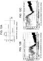
- charts B and charts C of FIG. 9A to FIG. 12C there are shown an average value and a peak value, respectively, of actually measured noise under a state in which the first offset voltage Voffset1 and the second offset voltage Voffset2 have a difference that satisfies a relationship of FIG. 9A .
- the vertical axis of the respective charts B and C represents an increasing noise level; specifically, a larger value on the vertical axis corresponds to a higher noise level. It follows that the noise level increases in the order of x0, x1, x2, x3, x4, x5, and x6.
- the noise level at x5 is lower than that at x6, the noise level at x4 is lower than that at x5, the noise level at x3 is lower than that at x4, the noise level at x2 is lower than that at x3, the noise level at x2 is lower than that at x3, the noise level at x1 is lower than that at x2, and the noise level at x0 is lower than that at x1.
- the average value of the 160 kHz noise components can be reduced to Xave3a that is smaller than x1 as shown in FIG. 11B
- the peak value thereof can be reduced down to Xpeak3a that is smaller than Xpeak2 of FIG. 10C , as shown in FIG. 11C .
- n is set to an "integer equal to or less than a value obtained by dividing fh by fc". With this operation, noise can be reduced within a range equal to or more than the lower limit frequency fr defined by the noise regulation, and equal to or less than the upper limit frequency fh thereof.
- n of Expression (1-20) is output while being caused to fluctuate at a regular interval that is a positive integral multiple (1, 2, 3, ...) of a half cycle (Tc/2) of the PWM carrier wave PWMC, within a range of from the "integer equal to or more than a value obtained by dividing fr by fc" to the "integer equal to or less than a value obtained by dividing fh by fc", noise can be reduced in a wider range equal to or more than the lower limit frequency fr defined by the noise regulation, and equal to or less than the upper limit frequency fh thereof. For example, as compared with the case of FIG.
- a value obtained by subtracting Voffset2 from Voffset1 is set to fluctuate at a regular interval of 100 ⁇ s in the order of -1.5 V (-Vdc/8), 1.5 V (Vdc/8), -1 V (-Vdc/12), 1 V (Vdc/12), and -1.5 V (-Vdc/8) as shown in FIG. 12A so as to reduce noise in a frequency band of from 200 kHz to 300 kHz, the noise in a frequency band of from 150 kHz to 300 kHz can be reduced in a well-balanced manner in terms of an average value, as shown in FIG.
- the worst value in the range above can be reduced from Xave3b between X4 and X5 as shown in FIG. 11B down to Xave4b between X3 and X4 as shown in FIG. 12B .
- the peak noise can also be reduced from Xpeak3b substantially equal to X5 as shown in FIG. 11C down to Xpeak4b between X4 and X5 as shown in FIG. 12C .
- n is an integer, but n may not be an integer.
- a description is given below of how to reduce noise on the assumption that n is not necessarily an integer.
- n is required to satisfy Expression (1-21).
- the absolute value Vave_dif_abs of the differential voltage being a difference between the first average voltage and the second average voltage is output while being caused to fluctuate at a regular interval that is a positive integral multiple (1, 2, 3, ...) of half the cycle (Tc/2) of the PWM carrier wave PWMC, within a range that satisfies both of Expression (1-22) and Expression (1-24).
- the absolute value Vave_dif_abs of the differential voltage being a difference between the first average voltage Vave1 and the second average voltage Vave2 may be set as indicated by a curve of FIG. 13 at respective frequencies of noise to be reduced so that the absolute value of the differential voltage fluctuates within the frequency range of the noise to be reduced.
- noise can be reduced only by adjusting the differential voltage being a difference between the first average voltage and the second average voltage.
- the present invention is applicable to a case in which in-phase PWM carrier waves PWMC are applied to the first inverter and the second inverter and hence, it is not required to displace phases of the PWM carrier waves PWMC to be applied to the first inverter and the second inverter, so that the mounting operation is facilitated. Further, as can be seen from the fact that an operation of causing the frequencies of the plurality of PWM carrier waves PWMC to fluctuate is not required unlike the apparatus of Patent Literature 1, the mounting operation is easy to execute.
- Patent Literature 1 when it is required to reduce noise in a different frequency band, the apparatus of Patent Literature 1 is required to change the PWM carrier wave PWMC, leading to a problem that long adjustment time is required, whereas according to the present invention, noise can be reduced only by adjusting the differential voltage being a difference between the first average voltage and the second average voltage with reference to FIG. 13 , for example, leading to an advantageous effect that a desired change can be made easily and the adjustment time therefor can be reduced.
- the absolute value of the differential voltage being a difference between the first average voltage and the second average voltage may be set to 1.2 V with reference to FIG. 13 .
- the absolute value of the differential voltage being a difference between the first average voltage and the second average voltage may be set to 2 V.
- the first three-phase inverter and the second three-phase inverter are used by way of example, but the present invention is not limited to the three-phase configuration, and it is to be understood that the same effects can be produced by a first multi-phase inverter and a second multi-phase inverter, which have two or more phases.
- multi-phase drive voltage commands, multi-phase voltage commands, and other such commands are used as the three-phase drive voltage commands, the three-phase voltage commands, and other such commands.
- the absolute value Vave_dif_abs of the differential voltage Vave_dif being a difference between the first average voltage Vave1 and the second average voltage Vave2 is adjusted by adjusting the first offset voltage Voffset1 and the second offset voltage Voffset2 by way of example.
- the first average voltage Vave1 and the second average voltage Vave2 may be adjusted by adjusting a proportion of two zero-voltage vectors to be generated for the first multi-phase inverter (3a), that is, (V0 (corresponding to a switching pattern in which the switches Sun1, Svn1, and Swn1 on the negative side of the DC power supply are turned on in all phases; in the three-phase configuration example of FIG.
- the AC rotating machine having the two sets of three-phase windings is described by way of example, but the present invention is not limited thereto.
- the first three-phase inverter and the second three-phase inverter can be connected to different AC rotating machines.
- a voltage adjustment control unit 6a is configured to carry out the above-mentioned control such as adjustment of the absolute value Vave_dif_abs of the differential voltage Vave_dif being a difference between the first average voltage Vave1 and the second average voltage Vave2, which is executed by adjusting the first offset voltage Voffset1 and the second offset voltage Voffset2. Further, the voltage adjustment control unit 6a can adjust the first offset voltage Voffset1 and the second offset voltage Voffset2 in accordance with a frequency f of noise to be reduced, which is applied from the outside, with reference to FIG. 13 , for example.
- FIG. 14 is a diagram for illustrating an overall configuration of an electric power steering apparatus according to a second embodiment of the present invention.
- a driver turns a steering wheel 901 to the right or left to steer front wheels 902.
- a torque detecting device 903 is configured to detect a steering torque Ts of a steering system, and output the detected torque Ts to a control command generating unit 905 as described below.
- the AC rotating machine 1 is configured to generate an assist torque for assisting the driver in steering via a gear 904, and a rotor thereof is mechanically connected to the gear 904.
- the other configuration thereof is the same as that of the AC rotating machine 1 of FIG. 1 .
- the control command generating unit 905 is configured to calculate the control command CCO used to control the AC rotating machine 1 into a desired condition based on the driver's steering torque Ts output from a torque sensor 903.
- a torque current command I_target is calculated as represented by Expression (2-1).
- I _ target ka ⁇ Ts
- ka is a constant, which can be set to vary depending on the steering torque Ts or a travel speed of a vehicle.
- the torque current command I_target is determined based on Expression (2-1), but can be set through well-known compensation control executed in accordance with a steering condition.
- a current detecting device 201a is used to detect currents lu1, Iv1, and Iw1 that flow on an output side of the first three-phase inverter 3a, as current signals Iu1_c, Iv1_c, and Iw1_c, respectively, in the vicinity of the peak of the PWM carrier wave PWMC.
- peak used herein refers to the minimum value (-Vdc/2) or the maximum value (Vdc/2) of the PWM carrier wave PWMC.
- a current detecting device 201b is configured to detect currents Iu2, Iv2, and Iw2 that flow on the output side of the second three-phase inverter 3b as current signals Iu2_c, Iv2_c, and Iw2_c, respectively, in the vicinity of the peak of the PWM carrier wave PWMC.
- the drive voltage command calculation unit 4a is configured to calculate the first three-phase drive voltage commands Vu1_ref, Vv1_ref, and Vw1_ref and the second three-phase drive voltage commands Vu2_ref, Vv2_ref, and Vw2_ref, which are used to drive the AC rotating machine 1, based on the control command COO (I_target), the current signals Iu1_c, Iv1_c, and Iw1_c detected by the current detecting device 201a, and the current signals Iu2_c, Iv2_c, and Iw2_c detected by the current detecting device 201b.
- the first three-phase drive voltage commands Vu1_ref, Vv1_ref, and Vw1_ref are obtained by coordinate transformation, into voltage commands on stationary three-phase axes, of two-rotation-axes voltages obtained through proportional integration control of a difference between: two-rotation-axes currents obtained by coordinate transformation of the current signals Iu1_c, Iv1_c, and Iw1_c based on the rotational position of the AC rotating machine 1, or based on a publicly-known rotational position estimation method; and the torque current command I_target and an exciting current command.
- the second three-phase drive voltage commands Vu2_ref, Vv2_ref, and Vw2_ref are obtained by coordinate transformation, into voltage commands on stationary three-phase axes, of two-rotation-axes voltages obtained through proportional integration control of a difference between: two-rotation-axes currents obtained by coordinate transformation of the current signals Iu2_c, Iv2_c, and Iw2_c based on the rotational position of the AC rotating machine 1, or based on a publicly-known rotational position estimation method; and the control command I_target and an exciting current command.
- the primary importance of the electric power steering apparatus is a stability of each of the current detecting devices 201a and 201b. To ensure the stability in current control, it is required to detect at regular intervals a motor current, that is, the currents Iu1, Iv1, and Iw1, and the currents Iu2, Iv2, and Iw2.
- a motor current that is, the currents Iu1, Iv1, and Iw1, and the currents Iu2, Iv2, and Iw2.
- a triangular wave that repeats itself at the same cycle is used as the PWM carrier wave PWMC, and the motor current is detected in the vicinity of the peak thereof.
- the PWM carrier wave PWMC with the same cycle is used, and thus a period between the vicinity of a peak of the PWM carrier wave PWMC in one cycle and the vicinity of a peak of the PWM carrier wave PWMC in the next cycle is constant all the time. Therefore, the motor current can be detected at regular intervals, to thereby ensure the stability of each of the current detecting devices 201a and 201b.
- the current is detected at a timing in the vicinity of the peak of the PWM carrier wave PWMC and hence, the fundamental wave thereof can be detected from the current containing a ripple component resulting from the PWM signal. Therefore, the current can be detected with high accuracy, and the torque ripple caused in the AC rotating machine 1 is not increased, so that a driver can have a favorable feeling in steering the steering wheel.
- Patent Literature 1 cannot ensure both of noise reduction and high-accuracy, stable current control.
- the triangular wave with the same cycle is used as the PWM carrier wave PWMC
- the current detecting device is caused to detect the motor current at a timing in the vicinity of the peak of the PWM carrier wave PWMC
- the drive command voltage calculation unit is configured to calculate a voltage command based on the current detected at the timing.
- a control unit 100 having the respective functions as illustrated in FIG. 1 and FIG. 14 may be configured by different control circuits, or configured by a single integrated control circuit.
- each of the processing circuits for implementing those functions may be constructed by dedicated hardware or a central processing unit (CPU, which is also referred to as “processing unit”, “arithmetic unit”, “microprocessor”, “microcomputer”, “processor”, or “DSP”) for executing a program stored in a memory.
- CPU central processing unit
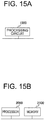
- FIG. 15A and FIG. 15B are schematic illustrations of hardware configurations in a case where those functions are constructed by hardware and a case where those functions are constructed by software, respectively.
- a processing circuit 1000 corresponds to, for example, a single circuit, a complex circuit, a programmed processor, a processor for a parallel program, an ASIC, an FPGA, or a combination thereof.
- the functions of the above-mentioned respective components may be implemented by a processing circuit, or the functions of the components may altogether be implemented by a processing circuit.
- the functions of the respective components are constructed by a CPU illustrated in FIG. 15B
- the functions of the respective components are implemented by software, firmware, or a combination of software and firmware.
- the software and the firmware are described as programs, and are stored in a memory 2100.
- a processor 2000 which is a processing circuit, reads out and executes the programs stored in the memory 2100, to thereby implement the functions of the respective components.
- Those programs may be considered as programs for causing a computer to execute the procedures and the methods of the respective components.
- the memory 2100 corresponds to, for example, a nonvolatile or volatile semiconductor memory such as a RAM, a ROM, a flash memory, an EPROM, or an EEPROM, or to a magnetic disk, a flexible disk, an optical disc, a compact disc, a mini disc, or a DVD.
- a nonvolatile or volatile semiconductor memory such as a RAM, a ROM, a flash memory, an EPROM, or an EEPROM, or to a magnetic disk, a flexible disk, an optical disc, a compact disc, a mini disc, or a DVD.
- the processing circuit can implement each of the above-mentioned functions by hardware, software, firmware, or a combination thereof.
- various types of information required for the processing are set to the circuit in advance in the case of the hardware configuration, and are stored in the memory in advance in the case of the software configuration.
- the power conversion device includes:
- the voltage adjustment control unit (6a) is configured to, when fh represents an upper limit frequency defined by noise regulation to which the power conversion device is required to conform, control the first average voltage adjustment unit (5a) and the second average voltage adjustment unit (5b) so that an absolute value of the differential voltage (Vave_dif_abs) is equal to or more than a value derived from Expression (2): k 2 ⁇ fc / fh ⁇ Vdc V
- the voltage adjustment control unit (6a) is configured to control the first average voltage adjustment unit (5a) and the second average voltage adjustment unit (5b) so that the absolute value of the differential voltage (Vave_dif_abs) is changed in a range equal to or less than the value derived from Expression (1), and equal to or more than the value derived from Expression (2) at a regular interval that is a positive integral multiple of a half cycle of the PWM signal.
- the power conversion device includes:
- the voltage adjustment control unit (6a) is configured to, when an upper limit frequency defined by the noise regulation to which the power conversion device is required to conform is represented by fh, set the value of n derived from Expression (3) to an integer equal to or less than (fh/fc) obtained by dividing fh by fc.
- the voltage adjustment control unit (6a) is configured to control the first average voltage adjustment unit (5a) and the second average voltage adjustment unit (5b) so as to change the (Vave_dif_abs) of the differential voltage by changing the value n at a regular interval that is a positive integral multiple of a half cycle of the PWM signal, as the differential voltage.
- the power conversion device includes:
- the voltage adjustment control unit (6a) is configured to set the differential voltage (Vave_diff) in a range including a value derived from Expression (5): ⁇ Vdc / 8 V
- the voltage adjustment control unit (6a) is configured to set the differential voltage (Vave_diff) in a range including a value derived from at least one of Expression (6) or (7): Vdc / 12 V ⁇ Vdc / 12 V
- the electric power steering apparatus includes:
- the power conversion device and the electric power steering apparatus according to one embodiment of the present invention are applicable to various types of power conversion devices and electric power steering apparatus.
Landscapes
- Engineering & Computer Science (AREA)
- Power Engineering (AREA)
- Chemical & Material Sciences (AREA)
- Combustion & Propulsion (AREA)
- Transportation (AREA)
- Mechanical Engineering (AREA)
- Inverter Devices (AREA)
- Control Of Ac Motors In General (AREA)
- Control Of Multiple Motors (AREA)
Description
- The present invention relates to a power conversion device and an electric power steering apparatus.
- Hitherto, there has been known a motor control apparatus configured as follows. That is, the motor control apparatus includes: a plurality of power converters; a plurality of motor command calculation units; and a plurality of carrier generation units, which are provided in association with a plurality of motors, respectively, in which the plurality of carrier generation units are each configured to generate a plurality of carrier signals, and a carrier frequency control unit is configured to control frequencies of the plurality of carrier signals so that the frequencies of the plurality of carrier signals fluctuate within a plurality of preset frequency ranges which are defined for each of the plurality of carrier signals. Further, the plurality of preset frequency ranges are determined in advance not to overlap one another, to thereby reduce noise generated by switching operations of the power converters (see Patent Literature 1).
- Further, there has been known a power conversion device configured as follows. That is, the power conversion device includes two inverters, in which a "flatbed two-phase modulation" is executed in one inverter unit, to subtract from all voltage command signals of three phases a value obtained by subtracting a preset lower limit value from the smallest voltage command signal among the voltage command signals of the three phases so that the smallest voltage command signal equals the preset lower limit value, and a "flattop two-phase modulation process" is executed in another inverter unit, to subtract from all voltage command signals of three phases a value obtained by subtracting a preset upper limit value from the largest voltage command signal among the voltage command signals of the three phases so that the largest voltage command signal equals the preset upper limit value. With this configuration, effective voltage vector generation periods in the two inverters are not overlapped, and hence a ripple current of a capacitor can be reduced (see Patent Literature 2).
-
- [PTL 1]
JP 5644854 B2 - [PTL 2]
JP 5045799 B2 - With the method described in
Patent Literature 1, in which a plurality of frequencies are set as a frequency of a pulse width modulation (PWM) carrier wave for respective inverters, and one of the frequencies is changed to be selected, it is required to store a plurality of PWM carrier waves and thus prepare a large memory capacity. Consequently, a control apparatus cannot be easily mounted to an inexpensive microcontroller (CPU). - Further, when a PWM carrier wave for each inverter is to be changed after the control apparatus is mounted to a CPU such as a microcontroller, this operation requires a large amount of time. Therefore, for example, when it is detected that a noise level of a certain frequency component exceeds a reference value by measuring noise in an end product and an additional operation of reducing noise is required, the noise level is required to be adjusted by further setting one or two more PWM carrier waves of different frequencies. In this case, a large amount of time is required to design and install an additional program to the microcontroller, possibly leading to shortage of the memory of the microcontroller.
- Further, with the method described in
Patent Literature 2, in which the "flatbed two-phase modulation process" is executed in one inverter, and the "flattop two-phase modulation process" is executed in another inverter, the voltage command signal in the one inverter is shifted to be as high as possible, and the voltage command signal in the another inverter is shifted to be as low as possible so as to avoid overlap of effective vectors. This method is effective to reduce a capacitor current within a wide range of modulation ratios, but is not directed to reducing noise generated by the two inverters and thus is not suitable for noise reduction. - The present invention has been made to solve the above-mentioned problems, and an object of the present invention is generally to provide an electric power steering apparatus and a power conversion device including two multi-phase inverters, which can suppress noise within a frequency band defined by noise regulation without changing a frequency of a PWM carrier wave of each inverter.
- According to one embodiment of the present invention, there are provided a power conversion device and the like including: a first multi-phase inverter and a second multi-phase inverter, which are configured to receive a DC voltage output from a DC power supply, and execute power conversion to convert the DC voltage into AC voltages and then output the resultant AC voltages; a drive voltage command calculation unit configured to calculate first multi-phase drive voltage commands and second multi-phase drive voltage commands, which cause the first multi-phase inverter and the second multi-phase inverter to drive a load based on an external control command; a first average voltage adjustment unit configured to output, as first multi-phase voltage commands, values obtained by adjusting the first multi-phase drive voltage commands with use of a first offset voltage, to thereby control the first multi-phase inverter; a second average voltage adjustment unit configured to output, as second multi-phase voltage commands, values obtained by adjusting the second multi-phase drive voltage commands with use of a second offset voltage, to thereby control the second multi-phase inverter; and a voltage adjustment control unit configured to, when the DC voltage of the DC power supply is represented by Vdc, a frequency of a PWM signal of each of the first multi-phase inverter and the second multi-phase inverter is represented by fc, and a lower limit frequency defined by noise regulation to which the power conversion device is required to conform is represented by fr, control the first average voltage adjustment unit and the second average voltage adjustment unit so that an absolute value of a differential voltage being a difference between: a first average voltage, which is an average value of the first multi-phase voltage commands of respective phases as command values for the AC voltages to be output from the first multi-phase inverter; and a second average voltage, which is an average value of the second multi-phase voltage commands of respective phases as command values for the AC voltages to be output from the second multi-phase inverter, is equal to or less than a value derived from Expression (1):

- According to the present invention, it is possible to provide the electric power steering apparatus and the power conversion device including two multi-phase inverters, which can suppress noise within a frequency band defined by noise regulation without changing a frequency of a PWM carrier wave of each inverter.
-
-
FIG. 1 is a diagram for illustrating an overall configuration of a power conversion device according to a first embodiment of the present invention. -
FIG. 2A and FIG. 2B are views for illustrating a configuration example of windings of an AC rotating machine in the power conversion device according to the present invention. -
FIG. 3 is a chart for showing an operation of a first three-phase inverter of the power conversion device according to the first embodiment of the present invention. -
FIG. 4 is a chart for showing an operation of a second three-phase inverter of the power conversion device according to the first embodiment of the present invention. -
FIG. 5 is a waveform chart for showing actually measured waveforms of conduction noise that propagates from the first and second three-phase inverters to a DC power supply side, in the first embodiment of the present invention. -
FIG. 6 is a waveform chart for showing actually measured waveforms of conduction noise that propagates from the first and second three-phase inverters to the DC power supply side, in the first embodiment of the present invention. -
FIG. 7 is a chart for showing an approximate waveform of noise ofFIG. 6 . -
FIG. 8 is a chart for showing a differential voltage being a difference between a first average voltage and a second average voltage, which is used to reduce noise in the first embodiment of the present invention. -
FIG. 9A, FIG. 9B and FIG. 9C are graphs, in whichFIG. 9B and FIG. 9C are graphs for showing an average point and a peak of actual measurement of noise, respectively, which are obtained when a first offset voltage and a second offset voltage have a difference as shown inFIG. 9A . -
FIG. 10A, FIG. 10B and FIG. 10C are graphs, in whichFIG. 10B and FIG. 10C are graphs for showing an average point and a peak of actual measurement of noise, respectively, which are obtained when the first offset voltage and the second offset voltage have a difference as shown inFIG. 10A . -
FIG. 11A, FIG. 11B and FIG. 11C are graphs, in whichFIG. 11B and FIG. 11C are graphs for showing an average point and a peak of actual measurement of noise, respectively, which are obtained when the first offset voltage and the second offset voltage have a difference as shown inFIG. 11A . -
FIG. 12A, FIG. 12B and FIG. 12C are graphs, in whichFIG. 12B and FIG. 12C are graphs for showing an average point and a peak of actual measurement of noise, respectively, which are obtained when the first offset voltage and the second offset voltage have a difference as shown inFIG. 12A , in the first embodiment of the present invention. -
FIG. 13 is a graph for showing a relationship between an absolute value |Voffset1 -Voffset2| of a difference between a first offset voltage Voffset1 and a second offset voltage Voffset2 and a frequency of noise to be reduced, in the first embodiment of the present invention. -
FIG. 14 is a diagram for illustrating an overall configuration of an electric power steering apparatus according to a second embodiment of the present invention. -
FIG. 15A and FIG. 15B are diagrams for illustrating an example of a hardware configuration of a control unit in the power conversion device and an electric power steering apparatus according to one embodiment of the present invention. - According to one embodiment of the present invention, an absolute value (Vave_dif_abs) of a differential voltage (Vave_dif) being a difference between a first average voltage (Vave1) and a second average voltage (Vave2) is set equal to or less than a value derived from Expression (1), the first average voltage (Vave1) being an average value of first voltage commands (Vu1_ref, Vv1_ref', and Vw1_ref') of respective phases and the second average voltage (Vave2) being an average value of second voltage commands (Vu2_ref', Vv2_ref', and Vw2_ref') of respective phases, the first and second voltage commands being command values for AC voltages to be output from a first multi-phase inverter and a second multi-phase inverter of a power conversion device, respectively:

- Vdc represents a DC voltage for the power conversion device, which is supplied from a DC power supply,
- fc represents a frequency of each PWM signal (Vu1, Vv1, and Vw1) output from the first multi-phase inverter and the second multi-phase inverter,
- fr represents a lower frequency limit defined by noise regulation to which the power conversion device is required to conform,
- k2 represents an odd number equal to or more than one.
- Specifically, with the configuration in which the absolute value of the differential voltage being a difference between the first average voltage and the second average voltage is set equal to or less than a value derived from Expression (1) above, noise of a frequency component equal to or more than the lower frequency limit fr defined by the noise regulation, can be reduced without changing the frequency fc of the PWM signal. With this configuration, a capacity of a memory of a CPU such as a microcontroller can be considerably saved, the device can be mounted to an inexpensive microcontroller (CPU) having a small memory capacity, and consequently, cost reduction is achieved.
- Now, a power conversion device and an electric power steering apparatus according to the present invention is described with reference to the drawings by way of embodiments. In the embodiments, the same or corresponding parts are denoted by the same symbols, and redundant description is omitted.
-
FIG. 1 is a diagram for illustrating an overall configuration of a power conversion device according to a first embodiment of the present invention. - An
AC rotating machine 1 includes two sets of three-phase windings, that is, first three-phase windings U1, V1, and W1, and second three-phase windings U2, V2, and W2. As illustrated inFIG. 2A and FIG. 2B , in theAC rotating machine 1, the first three-phase windings U1-V1-W1 ofFIG. 2A and the second three-phase windings U2-V2-W2 ofFIG. 2B are arranged in phase in terms of an electric angle, and neutral points N1 and N2 thereof are not electrically connected. - A
DC power supply 2 is configured to output a DC voltage Vdc to a first three-phase inverter 3a and a second three-phase inverter 3b. TheDC power supply 2 includes all devices that can output a DC voltage, such as a battery, a DC-DC converter, a diode rectifier, or a PWM rectifier. TheDC power supply 2 has a positive-side potential Vp and a negative-side potential Vn. - The first three-
phase inverter 3a is configured to execute PWM modulation through comparison with a PWM carrier wave having a frequency fc based on first three-phase voltage commands Vu1_ref', Vv1_ref', and Vw1_ref' as described later, so as to perform inverse conversion, that is, DC-AC conversion of the DC voltage Vdc received from theDC power supply 2, to thereby apply resultant AC voltages Vu1, Vv1, and Vw1 to the first three-phase windings U1, V1, and W1 of theAC rotating machine 1. Switches Sup1 to Swp1, and switches Sun1 to Swn1 are prepared by connecting, in inverse parallel, diodes and semiconductor switches that are any ones of IGBTs, bipolar transistors, MOS power transistors, and the like. - The second three-
phase inverter 3b is configured to execute PWM modulation through comparison with a PWM carrier wave having a frequency fc based on second three-phase voltage commands Vu2_ref', Vv2_ref', and Vw2_ref' as described later, so as to perform inverse conversion, that is, DC-AC conversion of the DC voltage Vdc received from theDC power supply 2, to thereby apply resultant AC voltages Vu2, Vv2, and Vw2 to the second three-phase windings U2, V2, and W2 of theAC rotating machine 1. Switches Sup2 to Swp2, and switches Sun2 to Swn2 are prepared by connecting, in inverse parallel, diodes and semiconductor switches that are any ones of IGBTs, bipolar transistors, MOS power transistors, and the like. - A drive voltage
command calculation unit 4a is configured to calculate first three-phase drive voltage commands Vu1_ref, Vv1_ref, and Vw1_ref and second three-phase drive voltage commands Vu2_ref, Vv2_ref, and Vw2_ref used to drive theAC rotating machine 1 in accordance with a control command CCO. - The first three-phase drive voltage commands Vu1_ref, Vv1_ref, and Vw1_ref and the second three-phase drive voltage commands Vu2_ref, Vv2_ref, and Vw2_ref are calculated based on publicly-known technologies as described below.
- One example is V/F control executed to determine amplitudes of the first three-phase drive voltage commands and the second three-phase drive voltage commands under a state in which a speed command or a frequency command f for the
AC rotating machine 1 is set as the control command CCO ofFIG. 1 . - Another example is current feedback control, in which a current command for the
AC rotating machine 1 is set as the control command CCO, and the first three-phase drive voltage commands Vu1_ref, Vv1_ref, and Vw1_ref are calculated through proportional-integral control so as to reduce to zero a deviation between the current command and values of currents flowing through the first three-phase windings U1, V1, and W1, and the second three-phase drive voltage commands Vu2_ref, Vv2_ref, and Vw2_ref are calculated through proportional-integral control so as to reduce to zero a deviation between the current command and values of currents flowing through the second three-phase windings U2, V2, and W2. - A first average
voltage adjustment unit 5a is configured to uniformly add a first offset voltage Voffset1 to the first three-phase drive voltage commands Vu1_ref, Vv1_ref, and Vw1_ref output from the drive voltagecommand calculation unit 4a, and then output the resultant commands as the first three-phase voltage commands Vu1_ref', Vv1_ref', and Vw1_ref'. - A first average voltage Vave1 as an average voltage of the first three-phase voltage commands Vu1_ref', Vv1_ref', and Vw1_ref' can be adjusted through adjustment of the first offset voltage Voffset1. This adjustment is described below.
- The first three-phase drive voltage commands Vu1_ref, Vv1_ref, and Vw1_ref can be derived from Expressions (1-1) to (1-3) as three-phase AC voltages. In Expressions (1-1) to (1-3), Vamp1 represents an amplitude of the respective first three-phase drive voltage commands, and θv1 represents a phase of the respective first three-phase drive voltage commands.


- Next, the first three-phase voltage commands Vu1_ref', Vv1_ref', and Vw1_ref' are obtained by adding the first offset voltage Voffset1 to the first three-phase drive voltage commands Vu1_ref, Vv1_ref, and Vw1_ref, and thus those commands are represented by Expressions (1-4) to (1-6).


- The first average voltage Vave1 is represented by Expression (1-7).

- As described above, the first average voltage Vave1 equals the first offset voltage Voffset1, and thus the first average voltage Vave1 can be adjusted through the adjustment of the first offset voltage Voffset1.
- A second average
voltage adjustment unit 5b is configured to uniformly add a second offset voltage Voffset2 to the second three-phase drive voltage commands Vu2_ref, Vv2_ref, and Vw2_ref output from the drive voltagecommand calculation unit 4a, and then output the resultant commands as the second three-phase voltage commands Vu2_ref', Vv2_ref', and Vw2_ref'. - A second average voltage Vave2 as an average voltage of the second three-phase voltage commands Vu2_ref', Vv2_ref', and Vw2_ref' can be adjusted through adjustment of the second offset voltage Voffset2. This adjustment is described below.
- The second three-phase drive voltage commands Vu2_ref, Vv2_ref, and Vw2_ref can be derived from Expressions (1-8) to (1-10) as three-phase AC voltages. In Expressions (1-8) to (1-10), Vamp2 represents an amplitude of the respective second three-phase drive voltage commands, and θv2 represents a phase of the respective second three-phase drive voltage commands.



- Next, the second three-phase voltage commands Vu2_ref', Vv2_ref', and Vw2_ref' are obtained by adding the second offset voltage Voffset2 to the second three-phase drive voltage commands Vu2_ref, Vv2_ref, and Vw2_ref, and thus those commands are represented by Expressions (1-11) to (1-13).


- The second average voltage Vave2 is represented by Expression (1-14).

- As described above, the second average voltage Vave2 equals the second offset voltage Voffset2, and thus the second average voltage Vave2 can be adjusted through the adjustment of the second offset voltage Voffset2.
- Next, a description is given of how to generate the AC voltages Vu1, Vv1, and Vw1 by the first three-
phase inverter 3a based on the first three-phase voltage commands Vu1_ref', Vv1_ref', and Vw1_ref' as command values for the AC voltages Vu1, Vv1, and Vw1 to be output from the first three-phase inverter 3a.FIG. 3 is a chart for showing how to generate the AC voltages Vu1, Vv1, and Vw1 in the first embodiment of the present invention. - In
FIG. 3 , operations of the switches Sup1, Svp1, and Swp1 on the positive side of the first three-phase inverter 3a are illustrated, and operations of the switches Sun1, Svn1, and Swn1, which operate inversely to the operations of the switches on the positive side, are not illustrated. - The first three-phase voltage command Vu1_ref' is compared to a PWM carrier wave PWMC with a cycle Tc (=1/fc), and when Vu1_ref' is larger than PWMC, the switch Sup1 is set to "1" (ON), and the switch Sun1, which is not illustrated in
FIG. 3 , is set to "0" (OFF). With this setting, the positive-side potential Vp of theDC power supply 2 is output as the AC voltage Vu1. - In contrast, when Vu1_ref' is smaller than PWMC, the switch Sup1 is set to "0" (OFF), and the switch Sun1 is set to "1" (ON). With this setting, the negative-side potential Vn of the
DC power supply 2 is output as the AC voltage Vu1. - In the above-mentioned comparison between the respective phase voltage commands and the PWMC, the case in which the respective phase voltage commands are "larger" or "smaller" than the PWMC is described, but the case in which the respective phase voltage commands are equal to the PWMC is not described. This is because in actuality, opening/closing operations of the switches of the respective three-phase inverters are controlled with use of a buffer so that series-connected switches are not turned on or off at the same time. A detailed description thereof is omitted here.
- The first three-phase voltage command Vv1_ref' is compared to a PWM carrier wave PWMC with a cycle Tc (=1/fc), and when Vv1_ref' is larger than PWMC, the switch Svp1 is set to "1" (ON), and the switch Svn1, which is not illustrated in
FIG. 3 , is set to "0" (OFF). With this setting, the positive-side potential Vp of theDC power supply 2 is output as the AC voltage Vv1. - In contrast, when Vv1_ref' is smaller than PWMC, the switch Svp1 is set to "0" (OFF), and the switch Svn1 is set to "1" (ON). With this setting, the negative-side potential Vn of the
DC power supply 2 is output as the AC voltage Vv1. - The first three-phase voltage command Vw1_ref' is compared to a PWM carrier wave PWMC with a cycle Tc (=1/fc), and when Vw1_ref' is larger than PWMC, the switch Swp1 is set to "1" (ON), and the switch Swn1, which is not illustrated in
FIG. 3 , is set to "0" (OFF). With this setting, the positive-side potential Vp of theDC power supply 2 is output as the AC voltage Vw1. - In contrast, when Vw1_ref' is smaller than PWMC, the switch Swp1 is set to "0" (OFF), and the switch Swn1 is set to "1" (ON). With this setting, the negative-side potential Vn of the
DC power supply 2 is output as the AC voltage Vw1. - Through the operation above, the AC voltages Vu1, Vv1, and Vw1 output from the first three-
phase inverter 3a are PWM voltages with the cycle Tc, that is, the frequency fc. The PWM voltage of the frequency fc is also referred to as "PWM signal", and the cycle thereof matches the cycle Tc (=1/fc) of the PWM carrier wave PWMC. Thus, the frequency thereof also matches the frequency fc of the PWM carrier wave PWMC. - Next, a description is given of how to generate the AC voltages Vu2, Vv2, and Vw2 by the second three-
phase inverter 3b based on the second three-phase voltage commands Vu2_ref', Vv2_ref', and Vw2_ref' as command values for the AC voltages Vu2, Vv2, and Vw2 to be output from the second three-phase inverter 3b.FIG. 4 is a chart for showing how to generate the AC voltages Vu2, Vv2, and Vw2 in the first embodiment of the present invention. - In
FIG. 4 , operations of the switches Sup2, Svp2, and Swp2 on the positive side of the second three-phase inverter 3b are illustrated, and operations of the switches Sun2, Svn2, and Swn2, which operate inversely to the operations of the switches on the positive side, are not illustrated. - The second three-phase voltage command Vu2_ref' is compared to a PWM carrier wave PWMC with a cycle Tc (=1/fc), and when Vu2_ref' is larger than PWMC, the switch Sup2 is set to "1" (ON), and the switch Sun2, which is not illustrated in
FIG. 4 , is set to "0" (OFF). With this setting, the positive-side potential Vp of theDC power supply 2 is output as the AC voltage Vu2. - In contrast, when Vu2_ref' is smaller than PWMC, the switch Sup2 is set to "0" (OFF), and the switch Sun2 is set to "1" (ON). With this setting, the negative-side potential Vn of the
DC power supply 2 is output as the AC voltage Vu2. - The second three-phase voltage command Vv2_ref' is compared to a PWM carrier wave PWMC with a cycle Tc (=1/fc), and when Vv2_ref' is larger than PWMC, the switch Svp2 is set to "1" (ON), and the switch Svn2, which is not illustrated in
FIG. 4 , is set to "0" (OFF). With this setting, the positive-side potential Vp of theDC power supply 2 is output as the AC voltage Vv2. - In contrast, when Vv2_ref' is smaller than PWMC, the switch Svp2 is set to "0" (OFF), and the switch Svn2 is set to "1" (ON). With this setting, the negative-side potential Vn of the
DC power supply 2 is output as the AC voltage Vv2. - The second three-phase voltage command Vw2_ref' is compared to a PWM carrier wave PWMC with a cycle Tc (=1/fc), and when Vw2_ref' is larger than PWMC, the switch Swp2 is set to "1" (ON), and the switch Swn2, which is not illustrated in
FIG. 4 , is set to "0" (OFF). With this setting, the positive-side potential Vp of theDC power supply 2 is output as the AC voltage Vw2. - In contrast, when Vw2_ref' is smaller than PWMC, the switch Swp2 is set to "0" (OFF), and the switch Swn2 is set to "1" (ON). With this setting, the negative-side potential Vn of the
DC power supply 2 is output as the AC voltage Vw2. - Through the operation above, the AC voltages Vu2, Vv2, and Vw2 output from the second three-
phase inverter 3b are PWM voltages with the frequency fc. - The AC voltages Vu1, Vv1, and Vw1 output from the first three-
phase inverter 3a and the AC voltages Vu2, Vv2, and Vw2 output from the second three-phase inverter 3b are voltages of a PWM waveform with the frequency fc and hence, conduction noise propagates from the first three-phase inverter 3a and the second three-phase inverter 3b to theDC power supply 2 side. -
FIG. 5 is a waveform chart for showing actually measured waveforms of the AC voltages Vu1 and Vu2 and conduction noise NIZ superimposed on the positive-side potential Vp of theDC power supply 2 under a state in which Vu1_ref and Vu2_ref are almost equal to each other, and Voffset1 and Voffset2 are set equal to each other. Here, the PWM carrier wave PWMC has the frequency of 20 kHz, and in-phase PWM carrier waves PWMC are applied to the first three-phase inverter 3a and the second three-phase inverter 3b. In this case, the AC voltages Vu1 and Vu2 are substantially equal and hence, the AC voltages Vu1 and Vu2 are substantially equal in terms of on time, that is, a time at which the potential changes from Vn to Vp, and are also substantially equal in terms of off time, that is, a time at which the potential changes from Vp to Vn. Regarding the waveform of the noise NIZ, pulsation appears at around time ton as the on time and at around time toff as the off time. -
FIG. 6 is a waveform chart for showing actually measured waveforms of the AC voltages Vu1 and Vu2 and conduction noise NIZ superimposed on the positive-side potential Vp of theDC power supply 2 under a state in which Vu1_ref and Vu2_ref are almost equal to each other, and Voffset2 is set larger than Voffset1. Here, the PWM carrier wave PWMC has the frequency of 20 kHz, and in-phase PWM carrier waves PWMC are applied to the first three-phase inverter 3a and the second three-phase inverter 3b. In this case, the on time of the AC voltage Vu2, that is, a time period in which the AC voltage Vu2 is at the potential Vp, is longer than the AC voltage Vu1, and thus the AC voltage Vu1 and the AC voltage Vu2 are different in terms of the on time and the off time. Regarding the waveform of the noise NIZ, pulsation appears at time ton_1 and time ton_2 as the on time of the AC voltage Vu1 and that of the AC voltage Vu2, respectively, with an amplitude smaller than that of the noise at the time ton ofFIG. 5 . Further, pulsation appears at time toff_1 and time toff_2 as the off time of the AC voltage Vu1 and that of the AC voltage Vu2, respectively, with an amplitude smaller than that of the noise at the time toff ofFIG. 5 . - A description is given of how to reduce noise through adjustment of a difference between Voffset1 and Voffset2, that is, a difference between the first average voltage Vave1 and the second average voltage Vave2.
- Now, two noise components enclosed by the dotted line P of
FIG. 6 are expressed by an approximate waveform ofFIG. 7 . - In
FIG. 7 , V represents the height of the respective noise components, Y represents the width of the respective noise components, and X represents an interval between the two noise components. - The PWM carrier wave PWMC has the cycle Tc, and thus this approximate waveform repeatedly appears at the cycle Tc. Thus, Fourier series expansion of the waveform of
FIG. 7 yields an n-th order component "an" with respect to the frequency fc of the PWM carrier wave PWMC, which is represented by Expression (1-15). In Expression (1-15), f(x) represents the approximate waveform, and 2π represents the cycle Tc of the PWM carrier wave PWMC.
- Of the elements of Expression (1-15) above, only the interval X between the two noise components can be adjusted by the difference between Voffset1 and Voffset2. Thus, it suffices that Expression (1-16) is satisfied to adjust the solution of Expression (1-15) to zero by using X.

- In Expression (1-16) above, k1 is an odd integer. Specifically, k1=...-9, -7, -5, -3, -1, 1, 3, 5, 7, 9..., for example. Solving Expression (1-16) for X gives Expression (1-17).

- Here, on the basis of the example of
FIG. 8 , Voffset_dif is represented by Expression (1-18) when X is set to an off interval between the two voltages V1 and V2 to be compared with the PWM carrier wave PWMC.
- Then, substituting Expression (1-17) to Expression (1-18) and solving Expression (1-18) for Voffset_dif gives Expression (1-19).

- As understood from the description above, a differential voltage being a difference between the first average voltage Vave1 and the second average voltage Vave2 used to reduce the n-th order noise component with respect to the frequency fc of the PWM carrier wave PWMC, may be set similar to Voffset_dif represented by Expression (1-19). Further, the n-th order noise component with respect to the frequency fc of the PWM carrier wave PWMC can be reduced when an absolute value Vave_dif_abs of the differential voltage Vave_dif being the difference between the first average voltage Vave1 and the second average voltage Vave2 satisfies Expression (1-20), regardless of which one of the first average voltage Vave1 and the second average voltage Vave2 is larger than the other. Here, Expression (1-20) is derived by replacing k1 of Expression (1-19) with k2. In Expression (1-20), k2 is an odd number equal to or more than one. Specifically, k2=1, 3, 5, 7, 9, ..., for example.

- A description is given of how to set n of Expression (1-20).
- The power conversion device as illustrated in
FIG. 1 is required to conform to noise regulation defined by, for example, comité international special des perturbations radioélectriques (CISPR). Of noise components subject to the regulation, conduction noise is generally regulated into a range of from 150 kHz to 30 MHz. To conform to the regulation, provided that fr represents a lower limit frequency of the noise regulation that the power conversion device is required to conform to, n is set to an "integer equal to or more than a value obtained by dividing fr by fc". With this operation, noise in a frequency band equal to or higher than fr can be reduced. - For example, when fr is set to 150 kHz, and fc is set to 20 kHz, the minimum value of "integers obtained by dividing fr by fc" is eight and hence, k2 of Expression (1-20) is set to one, and Voffset1 and Voffset2 are set so that the differential voltage Vave_dif being a difference between the first average voltage and the second average voltage satisfies Vdc/8. With this operation, a 160 kHz noise component can be reduced.
- For example, in a case where the DC voltage Vdc is set to 12 V, when the difference between Voffset1 and Voffset2 is fixed to zero as illustrated in
FIG. 9A , a 160 kHz noise component has an average value Xave1, which is larger than x5 as illustrated inFIG. 9B , and has a peak value Xpeak1, which is larger than x5. - In charts B and charts C of
FIG. 9A to FIG. 12C , there are shown an average value and a peak value, respectively, of actually measured noise under a state in which the first offset voltage Voffset1 and the second offset voltage Voffset2 have a difference that satisfies a relationship ofFIG. 9A . - In
FIG. 9A to FIG. 12C , the vertical axis of the respective charts B and C represents an increasing noise level; specifically, a larger value on the vertical axis corresponds to a higher noise level. It follows that the noise level increases in the order of x0, x1, x2, x3, x4, x5, and x6. Specifically, the noise level at x5 is lower than that at x6, the noise level at x4 is lower than that at x5, the noise level at x3 is lower than that at x4, the noise level at x2 is lower than that at x3, the noise level at x2 is lower than that at x3, the noise level at x1 is lower than that at x2, and the noise level at x0 is lower than that at x1. - Meanwhile, when the difference between Voffset1 and Voffset2 is fixed to 1.5 V (=Vdc/8=12/8) as shown in
FIG. 10A , the average value of the 160 kHz noise components is reduced down to Xave2 that is smaller than x2 as shown inFIG. 10B , and the peak value thereof is suitably reduced to Xpeak2 that is smaller than x3 as shown inFIG. 10C . - Further, as shown in
FIG. 11A , when an absolute value of the difference between Voffset1 and Voffset2 is set to be 1.5 V (=Vdc/8=12/8) in such a way that a value obtained by subtracting Voffset2 from Voffset1 is repeatedly switched between Vdc/8 and -Vdc/8 every 100 µs, the average value of the 160 kHz noise components can be reduced to Xave3a that is smaller than x1 as shown inFIG. 11B , and the peak value thereof can be reduced down to Xpeak3a that is smaller than Xpeak2 ofFIG. 10C , as shown inFIG. 11C . Further, when fh represents an upper limit frequency defined by noise regulation that the power conversion device is required to conform to, n is set to an "integer equal to or less than a value obtained by dividing fh by fc". With this operation, noise can be reduced within a range equal to or more than the lower limit frequency fr defined by the noise regulation, and equal to or less than the upper limit frequency fh thereof. - Further, when n of Expression (1-20) is output while being caused to fluctuate at a regular interval that is a positive integral multiple (1, 2, 3, ...) of a half cycle (Tc/2) of the PWM carrier wave PWMC, within a range of from the "integer equal to or more than a value obtained by dividing fr by fc" to the "integer equal to or less than a value obtained by dividing fh by fc", noise can be reduced in a wider range equal to or more than the lower limit frequency fr defined by the noise regulation, and equal to or less than the upper limit frequency fh thereof. For example, as compared with the case of
FIG. 11A , in which an absolute value of the difference between Voffset1 and Voffset2 is set to 1.5 V (=Vdc/8), when a value obtained by subtracting Voffset2 from Voffset1 is set to fluctuate at a regular interval of 100 µs in the order of -1.5 V (-Vdc/8), 1.5 V (Vdc/8), -1 V (-Vdc/12), 1 V (Vdc/12), and -1.5 V (-Vdc/8) as shown inFIG. 12A so as to reduce noise in a frequency band of from 200 kHz to 300 kHz, the noise in a frequency band of from 150 kHz to 300 kHz can be reduced in a well-balanced manner in terms of an average value, as shown inFIG. 12B . Thus, the worst value in the range above can be reduced from Xave3b between X4 and X5 as shown inFIG. 11B down to Xave4b between X3 and X4 as shown inFIG. 12B . Further, as shown inFIG. 12C , the peak noise can also be reduced from Xpeak3b substantially equal to X5 as shown inFIG. 11C down to Xpeak4b between X4 and X5 as shown inFIG. 12C . - In the description above, n is an integer, but n may not be an integer. Thus, a description is given below of how to reduce noise on the assumption that n is not necessarily an integer. In Expression (1-20), in order to reduce a noise component having a frequency equal to or more than the lower limit frequency fr defined by the noise regulation that the power conversion device is required to conform to, n is required to satisfy Expression (1-21).

- Substituting Expression (1-21) into Expression (1-20) gives Expression (1-22).

- Thus, when the first average voltage Vave1 and the second average voltage Vave2 are set so that an absolute value Vave_dif_abs of the differential voltage being a difference between the first average voltage and the second average voltage satisfies Expression (1-22), it is possible to reduce the noise component having a frequency equal to or more than the lower limit frequency fr defined by the noise regulation to which the power conversion device is required to conform to. Further, in Expression (1-20), in order to reduce a noise component having a frequency equal to or less than the upper limit frequency fh defined by the noise regulation to which the power conversion device is required to conform to, n is required to satisfy Expression (1-23).
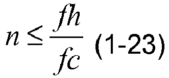
- Substituting Expression (1-23) into Expression (1-20) gives Expression (1-24).

- Thus, when the first average voltage Vave1 and the second average voltage Vave2 are set so that an absolute value Vave_dif_abs of the differential voltage being a difference between the first average voltage and the second average voltage satisfies Expression (1-24), it is possible to reduce the noise component having a frequency equal to or less than the upper limit frequency fh defined by the noise regulation to which the power conversion device is required to conform to. Further, the absolute value Vave_dif_abs of the differential voltage being a difference between the first average voltage and the second average voltage is output while being caused to fluctuate at a regular interval that is a positive integral multiple (1, 2, 3, ...) of half the cycle (Tc/2) of the PWM carrier wave PWMC, within a range that satisfies both of Expression (1-22) and Expression (1-24). With this operation, noise can be reduced in a wider frequency range as in the example of
FIG. 12B which gives the above-mentioned effects in comparison with the example ofFIG. 11B . More specifically, the absolute value Vave_dif_abs of the differential voltage being a difference between the first average voltage Vave1 and the second average voltage Vave2, may be set as indicated by a curve ofFIG. 13 at respective frequencies of noise to be reduced so that the absolute value of the differential voltage fluctuates within the frequency range of the noise to be reduced. -
FIG. 13 is a graph for showing a relationship between the absolute value Vave_dif_abs of the differential voltage Vave_dif being a difference between the first average voltage Vave1 and the second average voltage Vave2, which set placed on the vertical axis, and a frequency of noise to be reduced, which is set on the horizontal axis, under a state in which Vdc=12 V and fc=20 kHz. - As understood from the description above, in the first embodiment, noise can be reduced only by adjusting the differential voltage being a difference between the first average voltage and the second average voltage. The present invention is applicable to a case in which in-phase PWM carrier waves PWMC are applied to the first inverter and the second inverter and hence, it is not required to displace phases of the PWM carrier waves PWMC to be applied to the first inverter and the second inverter, so that the mounting operation is facilitated. Further, as can be seen from the fact that an operation of causing the frequencies of the plurality of PWM carrier waves PWMC to fluctuate is not required unlike the apparatus of
Patent Literature 1, the mounting operation is easy to execute. - Further, regarding an end product, when it is required to reduce noise in a different frequency band, the apparatus of
Patent Literature 1 is required to change the PWM carrier wave PWMC, leading to a problem that long adjustment time is required, whereas according to the present invention, noise can be reduced only by adjusting the differential voltage being a difference between the first average voltage and the second average voltage with reference toFIG. 13 , for example, leading to an advantageous effect that a desired change can be made easily and the adjustment time therefor can be reduced. For example, when a 200 kHz noise component is to be reduced, the absolute value of the differential voltage being a difference between the first average voltage and the second average voltage may be set to 1.2 V with reference toFIG. 13 . Likewise, when a 120 kHz noise component is to be reduced, for example, the absolute value of the differential voltage being a difference between the first average voltage and the second average voltage may be set to 2 V. - Further, in the first embodiment, the first three-phase inverter and the second three-phase inverter are used by way of example, but the present invention is not limited to the three-phase configuration, and it is to be understood that the same effects can be produced by a first multi-phase inverter and a second multi-phase inverter, which have two or more phases. In this case, multi-phase drive voltage commands, multi-phase voltage commands, and other such commands are used as the three-phase drive voltage commands, the three-phase voltage commands, and other such commands.
- Further, in the first embodiment, the absolute value Vave_dif_abs of the differential voltage Vave_dif being a difference between the first average voltage Vave1 and the second average voltage Vave2 is adjusted by adjusting the first offset voltage Voffset1 and the second offset voltage Voffset2 by way of example.
- However, when spatial vector modulation is employed to generate a PWM signal, the first average voltage Vave1 and the second average voltage Vave2 may be adjusted by adjusting a proportion of two zero-voltage vectors to be generated for the first multi-phase inverter (3a), that is, (V0 (corresponding to a switching pattern in which the switches Sun1, Svn1, and Swn1 on the negative side of the DC power supply are turned on in all phases; in the three-phase configuration example of
FIG. 3 , switch Sup1=0 (OFF), switch Svp1=0 (OFF), and switch Swp1=0 (OFF)), and V7 (corresponding to a switching pattern in which the switches Sup1, Svp1, and Swp1 on the positive side of the DC power supply are turned on in all phases; in the three-phase configuration example ofFIG. 3 , switch Sup1=1 (ON), switch Svp1=1 (ON), and switch Swp1=1 (ON)), and a proportion of two zero-voltage vectors to be generated for the second multi-phase inverter (3b), that is, (V0 (corresponding to a switching pattern in which the switches Sun2, Svn2, and Swn2 on the negative side of the DC power supply are turned on in all phases; in the three-phase configuration example ofFIG. 4 , switch Sup2=0 (OFF), switch Svp2=0 (OFF), and switch Swp2=0 (OFF)) and V7 (corresponding to a switching pattern in which the switches Sup2, Svp2, and Swp2 on the positive side of the DC power supply are turned on in all phases; in the three-phase configuration example ofFIG. 4 , switch Sup2=1 (ON), switch Svp2=1 (ON), and switch Swp2=1 (ON)). - Further, in the first embodiment, as a load connected to the first three-phase inverter and the second three-phase inverter, the AC rotating machine having the two sets of three-phase windings is described by way of example, but the present invention is not limited thereto. For example, it is to be understood that the first three-phase inverter and the second three-phase inverter can be connected to different AC rotating machines.
- Here, a voltage
adjustment control unit 6a is configured to carry out the above-mentioned control such as adjustment of the absolute value Vave_dif_abs of the differential voltage Vave_dif being a difference between the first average voltage Vave1 and the second average voltage Vave2, which is executed by adjusting the first offset voltage Voffset1 and the second offset voltage Voffset2. Further, the voltageadjustment control unit 6a can adjust the first offset voltage Voffset1 and the second offset voltage Voffset2 in accordance with a frequency f of noise to be reduced, which is applied from the outside, with reference toFIG. 13 , for example. -
FIG. 14 is a diagram for illustrating an overall configuration of an electric power steering apparatus according to a second embodiment of the present invention. - A driver turns a
steering wheel 901 to the right or left to steerfront wheels 902. Atorque detecting device 903 is configured to detect a steering torque Ts of a steering system, and output the detected torque Ts to a controlcommand generating unit 905 as described below. TheAC rotating machine 1 is configured to generate an assist torque for assisting the driver in steering via agear 904, and a rotor thereof is mechanically connected to thegear 904. The other configuration thereof is the same as that of theAC rotating machine 1 ofFIG. 1 . - The control
command generating unit 905 is configured to calculate the control command CCO used to control theAC rotating machine 1 into a desired condition based on the driver's steering torque Ts output from atorque sensor 903. As the control command CCO to be output, a torque current command I_target is calculated as represented by Expression (2-1).
- In Expression (2-1), ka is a constant, which can be set to vary depending on the steering torque Ts or a travel speed of a vehicle. In this example, the torque current command I_target is determined based on Expression (2-1), but can be set through well-known compensation control executed in accordance with a steering condition.
- Subsequently, a current detecting
device 201a is used to detect currents lu1, Iv1, and Iw1 that flow on an output side of the first three-phase inverter 3a, as current signals Iu1_c, Iv1_c, and Iw1_c, respectively, in the vicinity of the peak of the PWM carrier wave PWMC. The term "peak" used herein refers to the minimum value (-Vdc/2) or the maximum value (Vdc/2) of the PWM carrier wave PWMC. In this embodiment, the PWM carrier wave PWMC is assumed to have a constant cycle Tc (=1/Fc). - A current detecting
device 201b is configured to detect currents Iu2, Iv2, and Iw2 that flow on the output side of the second three-phase inverter 3b as current signals Iu2_c, Iv2_c, and Iw2_c, respectively, in the vicinity of the peak of the PWM carrier wave PWMC. - The drive voltage
command calculation unit 4a is configured to calculate the first three-phase drive voltage commands Vu1_ref, Vv1_ref, and Vw1_ref and the second three-phase drive voltage commands Vu2_ref, Vv2_ref, and Vw2_ref, which are used to drive theAC rotating machine 1, based on the control command COO (I_target), the current signals Iu1_c, Iv1_c, and Iw1_c detected by the current detectingdevice 201a, and the current signals Iu2_c, Iv2_c, and Iw2_c detected by the current detectingdevice 201b. - The first three-phase drive voltage commands Vu1_ref, Vv1_ref, and Vw1_ref are obtained by coordinate transformation, into voltage commands on stationary three-phase axes, of two-rotation-axes voltages obtained through proportional integration control of a difference between: two-rotation-axes currents obtained by coordinate transformation of the current signals Iu1_c, Iv1_c, and Iw1_c based on the rotational position of the
AC rotating machine 1, or based on a publicly-known rotational position estimation method; and the torque current command I_target and an exciting current command. - Further, the second three-phase drive voltage commands Vu2_ref, Vv2_ref, and Vw2_ref are obtained by coordinate transformation, into voltage commands on stationary three-phase axes, of two-rotation-axes voltages obtained through proportional integration control of a difference between: two-rotation-axes currents obtained by coordinate transformation of the current signals Iu2_c, Iv2_c, and Iw2_c based on the rotational position of the
AC rotating machine 1, or based on a publicly-known rotational position estimation method; and the control command I_target and an exciting current command. - Advantageous effects in the second embodiment are described below. The primary importance of the electric power steering apparatus is a stability of each of the current detecting
devices devices - Next, it is required to detect a current flowing through the
AC rotating machine 1 with high accuracy for the control of the electric power steering. This is because when the detected current includes an error with respect to a fundamental wave thereof, the proportional integral control is executed so that the current with the error matches a current command value, with the result that torque ripple occurs in theAC rotating machine 1, and is transmitted to thesteering wheel 1 via thegear 904, to thereby impair a steering feeling of a driver. - To address this issue, in the second embodiment, the current is detected at a timing in the vicinity of the peak of the PWM carrier wave PWMC and hence, the fundamental wave thereof can be detected from the current containing a ripple component resulting from the PWM signal. Therefore, the current can be detected with high accuracy, and the torque ripple caused in the
AC rotating machine 1 is not increased, so that a driver can have a favorable feeling in steering the steering wheel. - On the other hand, with the method described in
Patent Literature 1, in which the cycle of the PWM carrier wave PWMC is changed, when a current is detected at regular intervals so as to ensure a stability of a drive voltage command calculation unit, the current cannot be necessarily detected in the vicinity of the peak of the PWM carrier wave PWMC, and the detected current includes an error resulting from a ripple component caused by the PWM signal. This impairs the feeling in steering the steering wheel. Further, when the motor current is detected at a timing in the vicinity of the peak of the PWM carrier wave PWMC in order to detect the motor current with high accuracy, the cycle of the PWM carrier wave PWMC is changed and hence, the current cannot be detected at regular intervals, which hinders stable control. In particular, when the PWM carrier wave PWMC has a long cycle, the motor current is detected at large intervals, leading to unstable current control. In view of the above, the method described inPatent Literature 1 cannot ensure both of noise reduction and high-accuracy, stable current control. - As described above, in the second embodiment, the triangular wave with the same cycle is used as the PWM carrier wave PWMC, the current detecting device is caused to detect the motor current at a timing in the vicinity of the peak of the PWM carrier wave PWMC, and the drive command voltage calculation unit is configured to calculate a voltage command based on the current detected at the timing. This configuration produces a remarkable effect that cannot be produced by the related-art technology. Specifically, the effect of noise reduction described in the first embodiment can be achieved while maintaining the stability of current control and the favorable feeling in steering the steering wheel.
- In the respective embodiments above, a
control unit 100 having the respective functions as illustrated inFIG. 1 andFIG. 14 may be configured by different control circuits, or configured by a single integrated control circuit. - Regarding this point, each of the processing circuits for implementing those functions may be constructed by dedicated hardware or a central processing unit (CPU, which is also referred to as "processing unit", "arithmetic unit", "microprocessor", "microcomputer", "processor", or "DSP") for executing a program stored in a memory.
-
FIG. 15A and FIG. 15B are schematic illustrations of hardware configurations in a case where those functions are constructed by hardware and a case where those functions are constructed by software, respectively. - When the functions of the above-mentioned respective components are constructed by hardware illustrated in
FIG. 15A , aprocessing circuit 1000 corresponds to, for example, a single circuit, a complex circuit, a programmed processor, a processor for a parallel program, an ASIC, an FPGA, or a combination thereof. The functions of the above-mentioned respective components may be implemented by a processing circuit, or the functions of the components may altogether be implemented by a processing circuit. - When the functions of the above-mentioned respective components are constructed by a CPU illustrated in
FIG. 15B , the functions of the respective components are implemented by software, firmware, or a combination of software and firmware. The software and the firmware are described as programs, and are stored in amemory 2100. Aprocessor 2000, which is a processing circuit, reads out and executes the programs stored in thememory 2100, to thereby implement the functions of the respective components. Those programs may be considered as programs for causing a computer to execute the procedures and the methods of the respective components. In this case, thememory 2100 corresponds to, for example, a nonvolatile or volatile semiconductor memory such as a RAM, a ROM, a flash memory, an EPROM, or an EEPROM, or to a magnetic disk, a flexible disk, an optical disc, a compact disc, a mini disc, or a DVD. - The functions of the respective components may be implemented partially by dedicated hardware, and partially by software or firmware.
- In this way, the processing circuit can implement each of the above-mentioned functions by hardware, software, firmware, or a combination thereof.
- Moreover, various types of information required for the processing are set to the circuit in advance in the case of the hardware configuration, and are stored in the memory in advance in the case of the software configuration.
- As described above, the power conversion device according to one embodiment of the present invention includes:
- a first multi-phase inverter (3a) and a second multi-phase inverter (3b), which are configured to receive a DC voltage output from a DC power supply (2), and execute power conversion to convert the DC voltage into AC voltages and then output the resultant AC voltages;
- a drive voltage command calculation unit (4a) configured to calculate first multi-phase drive voltage commands (Vu1_ref, Vv1_ref, Vw1_ref) and second multi-phase drive voltage commands (Vu2_ref, Vv2_ref, Vw2_ref), which cause the first multi-phase inverter (3a) and the second multi-phase inverter (3b) to drive a load based on an external control command (CCO);
- a first average voltage adjustment unit (5a) configured to output, as first multi-phase voltage commands (Vu1_ref', Vv1_ref', Vw1_ref'), values obtained by adjusting the first multi-phase drive voltage commands (Vu1_ref, Vv1_ref, Vw1_ref) with use of a first offset voltage (Voffset1), to thereby control the first multi-phase inverter (3a);
- a second average voltage adjustment unit (5b) configured to output, as second multi-phase voltage commands (Vu2_ref, Vv2_ref', Vw2_ref), values obtained by adjusting the second multi-phase drive voltage commands (Vu2_ref, Vv2_ref, Vw2_ref) with use of a second offset voltage (Voffset2), to thereby control the second multi-phase inverter (3b); and
- a voltage adjustment control unit (6a) configured to,
- when the DC voltage of the DC power supply (2) is represented by Vdc, a frequency of a PWM signal (Vu1, Vv1, Vw1, Vu2, Vv2, Vw2) of each of the first multi-phase inverter (3a) and the second multi-phase inverter (3b) is represented by fc, and a lower limit frequency defined by noise regulation to which the power conversion device is required to conform is represented by fr, control the first average voltage adjustment unit (5a) and the second average voltage adjustment unit (5b) so that an absolute value (Vave_dif_abs) of a differential voltage (Vave_dif) being a difference between: a first average voltage (Vave1), which is an average value of the first multi-phase voltage commands (Vu1_ref', Vv1_ref', Vw1_ref') of respective phases as command values for the AC voltages to be output from the first multi-phase inverter (3a); and a second average voltage (Vave2), which is an average value of the second multi-phase voltage commands (Vu2_ref', Vv2_ref', Vw2_ref') of respective phases as command values for the AC voltages to be output from the second multi-phase inverter (3b), is equal to or less than a value derived from Expression (1):

- Further, the voltage adjustment control unit (6a) is configured to,
when fh represents an upper limit frequency defined by noise regulation to which the power conversion device is required to conform,
control the first average voltage adjustment unit (5a) and the second average voltage adjustment unit (5b) so that an absolute value of the differential voltage (Vave_dif_abs) is equal to or more than a value derived from Expression (2):
- Further, the voltage adjustment control unit (6a) is configured to control the first average voltage adjustment unit (5a) and the second average voltage adjustment unit (5b) so that the absolute value of the differential voltage (Vave_dif_abs) is changed in a range equal to or less than the value derived from Expression (1), and equal to or more than the value derived from Expression (2) at a regular interval that is a positive integral multiple of a half cycle of the PWM signal.
- Further, the power conversion device according to one embodiment of the present invention includes:
- a first multi-phase inverter (3a) and a second multi-phase inverter (3b), which are configured to receive a DC voltage output from a DC power supply (2), and execute power conversion to convert the DC voltage into AC voltages and then output the resultant AC voltages;
- a drive voltage command calculation unit (4a) configured to calculate first multi-phase drive voltage commands (Vu1_ref, Vv1_ref, Vw1_ref) and second multi-phase drive voltage commands (Vu2_ref, Vv2_ref, Vw2_ref), which cause the first multi-phase inverter (3a) and the second multi-phase inverter (3b) to drive a load based on an external control command (CCO);
- a first average voltage adjustment unit (5a) configured to output, as first multi-phase voltage commands (vu1_ref', Vv1_ref', Vw1_ref'), values obtained by adjusting the first multi-phase drive voltage commands (Vu1_ref, Vv1_ref, Vw1_ref) with use of a first offset voltage (Voffset1), to thereby control the first multi-phase inverter (3a);
- a second average voltage adjustment unit (5b) configured to output, as second multi-phase voltage commands (vu2_ref', Vv2_ref', Vw2_ref'), values obtained by adjusting the second multi-phase drive voltage commands (Vu2_ref, Vv2_ref, Vw2_ref) with use of a second offset voltage (Voffset2) to thereby control the second multi-phase inverter (3b); and
- a voltage adjustment control unit (6a) configured to,
- when the DC voltage of the DC power supply (2) is represented by Vdc, a frequency of a PWM signal (Vu1, Vv1, Vw1, Vu2, Vv2, Vw2) of each of the first multi-phase inverter (3a) and the second multi-phase inverter (3b) is represented by fc, and a lower limit frequency defined by noise regulation to which the power conversion device is required to conform is represented by fr,
- control the first average voltage adjustment unit (5a) and the second average voltage adjustment unit (5b) so that an absolute value (Vave_dif_abs) of a differential voltage (Vave_dif) being a difference between: a first average voltage (Vave1), which is an average value of the first multi-phase voltage commands (vu1_ref', Vv1_ref', Vw1_ref') of respective phases as command values for the AC voltages to be output from the first multi-phase inverter (3a); and a second average voltage (Vave2), which is an average value of the second multi-phase voltage commands (vu2_ref', Vv2_ref', Vw2_ref') of respective phases as command values for the AC voltages to be output from the second multi-phase inverter (3b), is a value derived from Expression (3):

- where the value of n is an integer equal to or more than (fr/fc) obtained by dividing fr by fc, and
- k2 represents an odd number equal to or more than one.
- Further, the voltage adjustment control unit (6a) is configured to, when an upper limit frequency defined by the noise regulation to which the power conversion device is required to conform is represented by fh, set the value of n derived from Expression (3) to an integer equal to or less than (fh/fc) obtained by dividing fh by fc.
- Further, the voltage adjustment control unit (6a) is configured to control the first average voltage adjustment unit (5a) and the second average voltage adjustment unit (5b) so as to change the (Vave_dif_abs) of the differential voltage by changing the value n at a regular interval that is a positive integral multiple of a half cycle of the PWM signal, as the differential voltage.
- Further, the power conversion device according to one embodiment of the present invention includes:
- a first multi-phase inverter (3a) and a second multi-phase inverter (3b), which are configured to receive a DC voltage output from a DC power supply (2), and execute power conversion to convert the DC voltage into AC voltages and then output the resultant AC voltages;
- a drive voltage command calculation unit (4a) configured to calculate first multi-phase drive voltage commands (Vu1_ref, Vv1_ref, Vw1_ref) and second multi-phase drive voltage commands (Vu2_ref, Vv2_ref, Vw2_ref), which cause the first multi-phase inverter (3a) and the second multi-phase inverter (3b) to drive a load based on an external control command (CCO);
- a first average voltage adjustment unit (5a) configured to output, as first multi-phase drive voltage commands (Vu1_ref', Vv1_ref', Vw1_ref'), values obtained by adjusting the first multi-phase drive voltage commands (Vu1_ref, Vv1_ref, Vw1_ref) with use of a first offset voltage (Voffset1), to thereby control the first multi-phase inverter (3a);
- a second average voltage adjustment unit (5b) configured to output, as second multi-phase voltage commands (vu2_ref', Vv2_ref', Vw2_ref'), values obtained by adjusting the second multi-phase drive voltage commands (Vu2_ref, Vv2_ref, Vw2_ref) with use of a second offset voltage (Voffset2), to thereby control the second multi-phase inverter (3b); and
- a voltage adjustment control unit (6a) configured to,
- when the DC voltage of the DC power supply (2) is represented by Vdc, a PWM signal of each of the first multi-phase inverter (3a) and the second multi-phase inverter (3b) has a frequency of 20 kHz, and an upper limit frequency defined by noise regulation to which the power conversion device is required to conform, is 150 kHz,
- control the first average voltage adjustment unit (5a) and the second average voltage adjustment unit (5b) so that a differential voltage (Vave_diff) being a difference between: a first average voltage (Vave1), which is an average value of the first multi-phase drive voltage commands (Vu1_ref', Vv1_ref', Vw1_ref') of respective phases as command values for the AC voltages to be output from the first multi-phase inverter (3a); and a second average voltage (Vave2), which is an average value of the second multi-phase voltage commands (vu2_ref', Vv2_ref', Vw2_ref') of respective phases as command values for the AC voltages to be output from the second multi-phase inverter (3b), is changed in a range including a value derived from Expression (4):

- Further, the voltage adjustment control unit (6a) is configured to set the differential voltage (Vave_diff) in a range including a value derived from Expression (5):

- Further, the voltage adjustment control unit (6a) is configured to set the differential voltage (Vave_diff) in a range including a value derived from at least one of Expression (6) or (7):


- Further, the electric power steering apparatus according to one embodiment of the present invention includes:
- any one of the power conversion devices described above; and
- an AC rotating machine (1) configured to generate an assist torque for assisting a driver in steering, by the first multi-phase inverter (3a) and the second multi-phase inverter (3b) applying the AC voltages.
- The power conversion device and the electric power steering apparatus according to one embodiment of the present invention are applicable to various types of power conversion devices and electric power steering apparatus.
- 1 AC rotating machine, 2 DC power supply, 3a, 3b three-phase inverter, 4a drive voltage command calculation unit, 5a first average voltage adjustment unit, 5b second average voltage adjustment unit, 6a voltage adjustment control unit, 100 control unit, 201a, 201b current detecting device, 901 handle, 902 front wheel, 903 torque sensor, 903 torque detecting device, 904 gear, 905 control command generating unit, 1000 processing circuit, 2000 processor, 2100 memory, Sup2, Svp2, Swp2 switch on positive side of DC power supply, Sun2, Svn2, Swn2 switch on negative side of DC power supply, U1, V1, W1, U2, V2, W2 phase winding
Claims (10)
- A power conversion device, comprising:a first multi-phase inverter and a second multi-phase inverter, which are configured to receive a DC voltage output from a DC power supply, and execute power conversion to convert the DC voltage into AC voltages and then output the resultant AC voltages;a drive voltage command calculation unit configured to calculate first multi-phase drive voltage commands and second multi-phase drive voltage commands, which cause the first multi-phase inverter and the second multi-phase inverter to drive a load based on an external control command;a first average voltage adjustment unit configured to output, as first multi-phase voltage commands, values obtained by adjusting the first multi-phase drive voltage commands with use of a first offset voltage, to thereby control the first multi-phase inverter;a second average voltage adjustment unit configured to output, as second multi-phase voltage commands, values obtained by adjusting the second multi-phase drive voltage commands with use of a second offset voltage, to thereby control the second multi-phase inverter; anda voltage adjustment control unit configured to,when the DC voltage of the DC power supply is represented by Vdc, a frequency of a PWM signal of each of the first multi-phase inverter and the second multi-phase inverter is represented by fc, and a lower limit frequency defined by noise regulation to which the power conversion device is required to conform is represented by fr,control the first average voltage adjustment unit and the second average voltage adjustment unit so that an absolute value of a differential voltage being a difference between: a first average voltage, which is an average value of the first multi-phase voltage commands of respective phases as command values for the AC voltages to be output from the first multi-phase inverter; and a second average voltage, which is an average value of the second multi-phase voltage commands of respective phases as command values for the AC voltages to be output from the second multi-phase inverter, is equal to or less than a value derived from Expression (1):

- The power conversion device according to claim 1, wherein the voltage adjustment control unit is configured to,
when an upper limit frequency defined by noise regulation to which the power conversion device is required to conform is represented by fh,
control the first average voltage adjustment unit and the second average voltage adjustment unit so that the absolute value of the differential voltage is equal to or more than a value derived from Expression (2):
- The power conversion device according to claim 2, wherein the voltage adjustment control unit is configured to control the first average voltage adjustment unit and the second average voltage adjustment unit so that the absolute value of the differential voltage is changed in a range equal to or less than the value derived from Expression (1), and equal to or more than the value derived from Expression (2) at a regular interval that is a positive integral multiple of a half cycle of the PWM signal.
- A power conversion device, comprising:a first multi-phase inverter and a second multi-phase inverter, which are configured to receive a DC voltage output from a DC power supply, and execute power conversion to convert the DC voltage into AC voltages and then output the resultant AC voltages;a drive voltage command calculation unit configured to calculate first multi-phase drive voltage commands and second multi-phase drive voltage commands, which cause the first multi-phase inverter and the second multi-phase inverter to drive a load based on an external control command;a first average voltage adjustment unit configured to output, as first multi-phase voltage commands, values obtained by adjusting the first multi-phase drive voltage commands with use of a first offset voltage, to thereby control the first multi-phase inverter;a second average voltage adjustment unit configured to output, as second multi-phase voltage commands, values obtained by adjusting the second multi-phase drive voltage commands with use of a second offset voltage, to thereby control the second multi-phase inverter; anda voltage adjustment control unit configured to,when the DC voltage of the DC power supply is represented by Vdc, a frequency of a PWM signal of each of the first multi-phase inverter and the second multi-phase inverter is represented by fc, and a lower limit frequency defined by noise regulation to which the power conversion device is required to conform is represented by fr,control the first average voltage adjustment unit and the second average voltage adjustment unit so that an absolute value of a differential voltage being a difference between: a first average voltage, which is an average value of the first multi-phase voltage commands of respective phases as command values for the AC voltages to be output from the first multi-phase inverter; and a second average voltage, which is an average value of the second multi-phase voltage commands of respective phases as command values for the AC voltages to be output from the second multi-phase inverter, is a value derived from Expression (3):

- The power conversion device according to claim 4, wherein the voltage adjustment control unit is configured to, when an upper limit frequency defined by the noise regulation to which the power conversion device is required to conform is represented by fh, set the value of n derived from Expression (3) to an integer equal to or less than fh/fc obtained by dividing fh by fc.
- The power conversion device according to claim 5, wherein the voltage adjustment control unit is configured to control the first average voltage adjustment unit and the second average voltage adjustment unit so as to change the absolute value of the differential voltage by changing the value n at a regular interval that is a positive integral multiple of a half cycle of the PWM signal, as the differential voltage.
- A power conversion device, comprising:a first multi-phase inverter and a second multi-phase inverter, which are configured to receive a DC voltage output from a DC power supply, and execute power conversion to convert the DC voltage into AC voltages and then output the resultant AC voltages;a drive voltage command calculation unit configured to calculate first multi-phase drive voltage commands and second multi-phase drive voltage commands, which cause the first multi-phase inverter and the second multi-phase inverter to drive a load based on an external control command;a first average voltage adjustment unit configured to output, as first multi-phase voltage commands, values obtained by adjusting the first multi-phase drive voltage commands with use of a first offset voltage, to thereby control the first multi-phase inverter;a second average voltage adjustment unit configured to output, as second multi-phase voltage commands, values obtained by adjusting the second multi-phase drive voltage commands with use of a second offset voltage, to thereby control the second multi-phase inverter; anda voltage adjustment control unit configured to,when the DC voltage of the DC power supply is represented by Vdc, a PWM signal of each of the first multi-phase inverter and the second multi-phase inverter has a frequency of 20 kHz, and an upper limit frequency defined by noise regulation to which the power conversion device is required to conform, is 150 kHz,control the first average voltage adjustment unit and the second average voltage adjustment unit so that a differential voltage being a difference between: a first average voltage, which is an average value of the first multi-phase voltage commands of respective phases as command values for the AC voltages to be output from the first multi-phase inverter; and a second average voltage, which is an average value of the second multi-phase voltage commands of respective phases as command values for the AC voltages to be output from the second multi-phase inverter, is changed in a range including a value derived from Expression (4):

- The power conversion device according to claim 7, wherein the voltage adjustment control unit is configured to set the differential voltage in a range including a value derived from Expression (5):

- The power conversion device according to claim 8, wherein the voltage adjustment control unit is configured to set the differential voltage in a range including a value derived from at least one of Expression (6) or (7):


- An electric power steering apparatus, comprising:the power conversion device of any one of claims 1 to 9; andan AC rotating machine configured to generate an assist torque for assisting a driver in steering, by the first multi-phase inverter and the second multi-phase inverter applying the AC voltages.
Applications Claiming Priority (1)
| Application Number | Priority Date | Filing Date | Title |
|---|---|---|---|
| PCT/JP2017/024353 WO2019008637A1 (en) | 2017-07-03 | 2017-07-03 | Power conversion device and electric power steering device |
Publications (3)
| Publication Number | Publication Date |
|---|---|
| EP3651351A1 true EP3651351A1 (en) | 2020-05-13 |
| EP3651351A4 EP3651351A4 (en) | 2020-06-24 |
| EP3651351B1 EP3651351B1 (en) | 2022-04-20 |
Family
ID=64949767
Family Applications (1)
| Application Number | Title | Priority Date | Filing Date |
|---|---|---|---|
| EP17916934.7A Active EP3651351B1 (en) | 2017-07-03 | 2017-07-03 | Power conversion device and electric power steering device |
Country Status (5)
| Country | Link |
|---|---|
| US (1) | US10965239B2 (en) |
| EP (1) | EP3651351B1 (en) |
| JP (1) | JP6768157B2 (en) |
| CN (1) | CN110832769B (en) |
| WO (1) | WO2019008637A1 (en) |
Cited By (2)
| Publication number | Priority date | Publication date | Assignee | Title |
|---|---|---|---|---|
| EP4135191A1 (en) * | 2021-08-10 | 2023-02-15 | Hyundai Motor Company | Motor driving apparatus |
| EP4187777A1 (en) * | 2021-11-26 | 2023-05-31 | Hyundai Motor Company | Motor drive device |
Families Citing this family (7)
| Publication number | Priority date | Publication date | Assignee | Title |
|---|---|---|---|---|
| JP7078051B2 (en) * | 2017-09-29 | 2022-05-31 | 日本電産株式会社 | Power converter, motor drive unit and electric power steering device |
| US11063547B2 (en) * | 2017-12-22 | 2021-07-13 | Mitsubishi Electric Corporation | Control device and control method for rotating electric machine |
| JP7372871B2 (en) * | 2020-04-16 | 2023-11-01 | 日立Astemo株式会社 | Motor control device, mechanical and electrical integrated unit, electric vehicle system, motor control method |
| CN112865664B (en) * | 2021-01-05 | 2022-08-30 | 奇瑞新能源汽车股份有限公司 | SVPWM control method and device for inverter of electric automobile and electric automobile |
| US12184213B2 (en) * | 2021-08-10 | 2024-12-31 | Hyundai Motor Company | Motor driving apparatus |
| JP7623922B2 (en) * | 2021-09-30 | 2025-01-29 | 日立Astemo株式会社 | Inverter control device, hybrid system, mechanical and electrical integrated unit, electric vehicle system, and inverter control method |
| WO2023073816A1 (en) * | 2021-10-26 | 2023-05-04 | 日立Astemo株式会社 | Motor control device, motor control method, hybrid system, pressure boosting convertor system, and electric power steering system |
Family Cites Families (11)
| Publication number | Priority date | Publication date | Assignee | Title |
|---|---|---|---|---|
| JPS54140379A (en) | 1978-04-20 | 1979-10-31 | Agency Of Ind Science & Technol | Method and device for sending constant volume of slurry by pressure |
| JP2001197779A (en) * | 2000-01-12 | 2001-07-19 | Nissan Motor Co Ltd | Motor drive |
| JP4645560B2 (en) * | 2006-08-31 | 2011-03-09 | パナソニック株式会社 | Motor drive device for washing and drying machine |
| EP2566040A1 (en) | 2010-04-28 | 2013-03-06 | Toyota Jidosha Kabushiki Kaisha | Device for controlling electric motor |
| JP5045799B2 (en) | 2010-08-27 | 2012-10-10 | 株式会社デンソー | Power conversion device, drive device, and electric power steering device using the same |
| JP6156282B2 (en) * | 2014-08-07 | 2017-07-05 | 株式会社デンソー | Rotating machine control device |
| CN107210702B (en) * | 2015-02-16 | 2019-08-13 | 三菱电机株式会社 | power conversion device |
| US10128739B2 (en) | 2015-02-16 | 2018-11-13 | Mitsubishi Electric Corporation | Power conversion device |
| JP6380156B2 (en) * | 2015-02-19 | 2018-08-29 | 株式会社デンソー | Power converter |
| JP6503277B2 (en) * | 2015-10-13 | 2019-04-17 | 東洋電機製造株式会社 | Controller and AC motor drive |
| JP6165216B2 (en) * | 2015-11-13 | 2017-07-19 | 三菱電機株式会社 | Method for manufacturing motor drive device |
-
2017
- 2017-07-03 US US16/614,513 patent/US10965239B2/en active Active
- 2017-07-03 WO PCT/JP2017/024353 patent/WO2019008637A1/en not_active Ceased
- 2017-07-03 EP EP17916934.7A patent/EP3651351B1/en active Active
- 2017-07-03 JP JP2019528204A patent/JP6768157B2/en active Active
- 2017-07-03 CN CN201780092595.XA patent/CN110832769B/en active Active
Cited By (4)
| Publication number | Priority date | Publication date | Assignee | Title |
|---|---|---|---|---|
| EP4135191A1 (en) * | 2021-08-10 | 2023-02-15 | Hyundai Motor Company | Motor driving apparatus |
| US11784604B2 (en) | 2021-08-10 | 2023-10-10 | Hyundai Motor Company | Motor driving apparatus |
| EP4187777A1 (en) * | 2021-11-26 | 2023-05-31 | Hyundai Motor Company | Motor drive device |
| US11936314B2 (en) | 2021-11-26 | 2024-03-19 | Hyundai Motor Company | Motor drive device |
Also Published As
| Publication number | Publication date |
|---|---|
| JP6768157B2 (en) | 2020-10-14 |
| CN110832769B (en) | 2022-10-04 |
| EP3651351B1 (en) | 2022-04-20 |
| WO2019008637A1 (en) | 2019-01-10 |
| EP3651351A4 (en) | 2020-06-24 |
| JPWO2019008637A1 (en) | 2019-11-07 |
| US10965239B2 (en) | 2021-03-30 |
| CN110832769A (en) | 2020-02-21 |
| US20200220488A1 (en) | 2020-07-09 |
Similar Documents
| Publication | Publication Date | Title |
|---|---|---|
| EP3651351B1 (en) | Power conversion device and electric power steering device | |
| US10291174B2 (en) | Control apparatus for power conversion apparatus | |
| US10199979B2 (en) | Power conversion device | |
| EP3477842B1 (en) | Power conversion device | |
| EP3364538B1 (en) | Ac rotating machine control device and electric power steering device equipped with same | |
| EP3651339B1 (en) | Inverter device and electric power steering device | |
| EP3261247B1 (en) | Power conversion device | |
| EP3570432B1 (en) | Motor control device | |
| EP3261246A1 (en) | Power conversion device | |
| US10666169B2 (en) | Control device for AC rotary machine and control device for electric power steering | |
| EP2372894B1 (en) | Direct-current to three-phase alternating-current inverter system | |
| EP2913915A1 (en) | Power conversion device | |
| EP3439163A1 (en) | Power converter | |
| EP3675352B1 (en) | Power conversion device and electric power steering device | |
| EP3675344B1 (en) | Power conversion device and electric power steering device | |
| EP4167459A1 (en) | Power conversion device and electric power steering device | |
| EP3206298A1 (en) | Power conversion device, method of controlling same, and electric power steering control device | |
| EP4376287A2 (en) | Servo system |
Legal Events
| Date | Code | Title | Description |
|---|---|---|---|
| STAA | Information on the status of an ep patent application or granted ep patent |
Free format text: STATUS: THE INTERNATIONAL PUBLICATION HAS BEEN MADE |
|
| PUAI | Public reference made under article 153(3) epc to a published international application that has entered the european phase |
Free format text: ORIGINAL CODE: 0009012 |
|
| STAA | Information on the status of an ep patent application or granted ep patent |
Free format text: STATUS: REQUEST FOR EXAMINATION WAS MADE |
|
| 17P | Request for examination filed |
Effective date: 20191114 |
|
| AK | Designated contracting states |
Kind code of ref document: A1 Designated state(s): AL AT BE BG CH CY CZ DE DK EE ES FI FR GB GR HR HU IE IS IT LI LT LU LV MC MK MT NL NO PL PT RO RS SE SI SK SM TR |
|
| AX | Request for extension of the european patent |
Extension state: BA ME |
|
| A4 | Supplementary search report drawn up and despatched |
Effective date: 20200525 |
|
| RIC1 | Information provided on ipc code assigned before grant |
Ipc: H02P 25/22 20060101AFI20200516BHEP Ipc: H02M 7/5387 20070101ALI20200516BHEP Ipc: H02M 7/493 20070101ALI20200516BHEP Ipc: H02P 27/08 20060101ALI20200516BHEP |
|
| DAV | Request for validation of the european patent (deleted) | ||
| DAX | Request for extension of the european patent (deleted) | ||
| REG | Reference to a national code |
Ref country code: DE Ref legal event code: R079 Ref document number: 602017056403 Country of ref document: DE Free format text: PREVIOUS MAIN CLASS: H02P0027060000 Ipc: H02P0025220000 |
|
| GRAP | Despatch of communication of intention to grant a patent |
Free format text: ORIGINAL CODE: EPIDOSNIGR1 |
|
| STAA | Information on the status of an ep patent application or granted ep patent |
Free format text: STATUS: GRANT OF PATENT IS INTENDED |
|
| RIC1 | Information provided on ipc code assigned before grant |
Ipc: H02M 7/493 20070101ALI20220105BHEP Ipc: H02M 7/5387 20070101ALI20220105BHEP Ipc: H02P 27/08 20060101ALI20220105BHEP Ipc: H02P 25/22 20060101AFI20220105BHEP |
|
| INTG | Intention to grant announced |
Effective date: 20220124 |
|
| GRAS | Grant fee paid |
Free format text: ORIGINAL CODE: EPIDOSNIGR3 |
|
| GRAA | (expected) grant |
Free format text: ORIGINAL CODE: 0009210 |
|
| STAA | Information on the status of an ep patent application or granted ep patent |
Free format text: STATUS: THE PATENT HAS BEEN GRANTED |
|
| AK | Designated contracting states |
Kind code of ref document: B1 Designated state(s): AL AT BE BG CH CY CZ DE DK EE ES FI FR GB GR HR HU IE IS IT LI LT LU LV MC MK MT NL NO PL PT RO RS SE SI SK SM TR |
|
| REG | Reference to a national code |
Ref country code: GB Ref legal event code: FG4D |
|
| REG | Reference to a national code |
Ref country code: CH Ref legal event code: EP |
|
| REG | Reference to a national code |
Ref country code: IE Ref legal event code: FG4D |
|
| REG | Reference to a national code |
Ref country code: DE Ref legal event code: R096 Ref document number: 602017056403 Country of ref document: DE |
|
| REG | Reference to a national code |
Ref country code: AT Ref legal event code: REF Ref document number: 1485989 Country of ref document: AT Kind code of ref document: T Effective date: 20220515 |
|
| REG | Reference to a national code |
Ref country code: LT Ref legal event code: MG9D |
|
| REG | Reference to a national code |
Ref country code: NL Ref legal event code: MP Effective date: 20220420 |
|
| REG | Reference to a national code |
Ref country code: AT Ref legal event code: MK05 Ref document number: 1485989 Country of ref document: AT Kind code of ref document: T Effective date: 20220420 |
|
| PG25 | Lapsed in a contracting state [announced via postgrant information from national office to epo] |
Ref country code: NL Free format text: LAPSE BECAUSE OF FAILURE TO SUBMIT A TRANSLATION OF THE DESCRIPTION OR TO PAY THE FEE WITHIN THE PRESCRIBED TIME-LIMIT Effective date: 20220420 |
|
| PG25 | Lapsed in a contracting state [announced via postgrant information from national office to epo] |
Ref country code: SE Free format text: LAPSE BECAUSE OF FAILURE TO SUBMIT A TRANSLATION OF THE DESCRIPTION OR TO PAY THE FEE WITHIN THE PRESCRIBED TIME-LIMIT Effective date: 20220420 Ref country code: PT Free format text: LAPSE BECAUSE OF FAILURE TO SUBMIT A TRANSLATION OF THE DESCRIPTION OR TO PAY THE FEE WITHIN THE PRESCRIBED TIME-LIMIT Effective date: 20220822 Ref country code: NO Free format text: LAPSE BECAUSE OF FAILURE TO SUBMIT A TRANSLATION OF THE DESCRIPTION OR TO PAY THE FEE WITHIN THE PRESCRIBED TIME-LIMIT Effective date: 20220720 Ref country code: LT Free format text: LAPSE BECAUSE OF FAILURE TO SUBMIT A TRANSLATION OF THE DESCRIPTION OR TO PAY THE FEE WITHIN THE PRESCRIBED TIME-LIMIT Effective date: 20220420 Ref country code: HR Free format text: LAPSE BECAUSE OF FAILURE TO SUBMIT A TRANSLATION OF THE DESCRIPTION OR TO PAY THE FEE WITHIN THE PRESCRIBED TIME-LIMIT Effective date: 20220420 Ref country code: GR Free format text: LAPSE BECAUSE OF FAILURE TO SUBMIT A TRANSLATION OF THE DESCRIPTION OR TO PAY THE FEE WITHIN THE PRESCRIBED TIME-LIMIT Effective date: 20220721 Ref country code: FI Free format text: LAPSE BECAUSE OF FAILURE TO SUBMIT A TRANSLATION OF THE DESCRIPTION OR TO PAY THE FEE WITHIN THE PRESCRIBED TIME-LIMIT Effective date: 20220420 Ref country code: ES Free format text: LAPSE BECAUSE OF FAILURE TO SUBMIT A TRANSLATION OF THE DESCRIPTION OR TO PAY THE FEE WITHIN THE PRESCRIBED TIME-LIMIT Effective date: 20220420 Ref country code: BG Free format text: LAPSE BECAUSE OF FAILURE TO SUBMIT A TRANSLATION OF THE DESCRIPTION OR TO PAY THE FEE WITHIN THE PRESCRIBED TIME-LIMIT Effective date: 20220720 Ref country code: AT Free format text: LAPSE BECAUSE OF FAILURE TO SUBMIT A TRANSLATION OF THE DESCRIPTION OR TO PAY THE FEE WITHIN THE PRESCRIBED TIME-LIMIT Effective date: 20220420 |
|
| PG25 | Lapsed in a contracting state [announced via postgrant information from national office to epo] |
Ref country code: RS Free format text: LAPSE BECAUSE OF FAILURE TO SUBMIT A TRANSLATION OF THE DESCRIPTION OR TO PAY THE FEE WITHIN THE PRESCRIBED TIME-LIMIT Effective date: 20220420 Ref country code: PL Free format text: LAPSE BECAUSE OF FAILURE TO SUBMIT A TRANSLATION OF THE DESCRIPTION OR TO PAY THE FEE WITHIN THE PRESCRIBED TIME-LIMIT Effective date: 20220420 Ref country code: LV Free format text: LAPSE BECAUSE OF FAILURE TO SUBMIT A TRANSLATION OF THE DESCRIPTION OR TO PAY THE FEE WITHIN THE PRESCRIBED TIME-LIMIT Effective date: 20220420 Ref country code: IS Free format text: LAPSE BECAUSE OF FAILURE TO SUBMIT A TRANSLATION OF THE DESCRIPTION OR TO PAY THE FEE WITHIN THE PRESCRIBED TIME-LIMIT Effective date: 20220820 |
|
| REG | Reference to a national code |
Ref country code: DE Ref legal event code: R097 Ref document number: 602017056403 Country of ref document: DE |
|
| PG25 | Lapsed in a contracting state [announced via postgrant information from national office to epo] |
Ref country code: SM Free format text: LAPSE BECAUSE OF FAILURE TO SUBMIT A TRANSLATION OF THE DESCRIPTION OR TO PAY THE FEE WITHIN THE PRESCRIBED TIME-LIMIT Effective date: 20220420 Ref country code: SK Free format text: LAPSE BECAUSE OF FAILURE TO SUBMIT A TRANSLATION OF THE DESCRIPTION OR TO PAY THE FEE WITHIN THE PRESCRIBED TIME-LIMIT Effective date: 20220420 Ref country code: RO Free format text: LAPSE BECAUSE OF FAILURE TO SUBMIT A TRANSLATION OF THE DESCRIPTION OR TO PAY THE FEE WITHIN THE PRESCRIBED TIME-LIMIT Effective date: 20220420 Ref country code: EE Free format text: LAPSE BECAUSE OF FAILURE TO SUBMIT A TRANSLATION OF THE DESCRIPTION OR TO PAY THE FEE WITHIN THE PRESCRIBED TIME-LIMIT Effective date: 20220420 Ref country code: DK Free format text: LAPSE BECAUSE OF FAILURE TO SUBMIT A TRANSLATION OF THE DESCRIPTION OR TO PAY THE FEE WITHIN THE PRESCRIBED TIME-LIMIT Effective date: 20220420 Ref country code: CZ Free format text: LAPSE BECAUSE OF FAILURE TO SUBMIT A TRANSLATION OF THE DESCRIPTION OR TO PAY THE FEE WITHIN THE PRESCRIBED TIME-LIMIT Effective date: 20220420 |
|
| PLBE | No opposition filed within time limit |
Free format text: ORIGINAL CODE: 0009261 |
|
| STAA | Information on the status of an ep patent application or granted ep patent |
Free format text: STATUS: NO OPPOSITION FILED WITHIN TIME LIMIT |
|
| PG25 | Lapsed in a contracting state [announced via postgrant information from national office to epo] |
Ref country code: MC Free format text: LAPSE BECAUSE OF FAILURE TO SUBMIT A TRANSLATION OF THE DESCRIPTION OR TO PAY THE FEE WITHIN THE PRESCRIBED TIME-LIMIT Effective date: 20220420 |
|
| REG | Reference to a national code |
Ref country code: CH Ref legal event code: PL |
|
| 26N | No opposition filed |
Effective date: 20230123 |
|
| GBPC | Gb: european patent ceased through non-payment of renewal fee |
Effective date: 20220720 |
|
| REG | Reference to a national code |
Ref country code: BE Ref legal event code: MM Effective date: 20220731 |
|
| PG25 | Lapsed in a contracting state [announced via postgrant information from national office to epo] |
Ref country code: AL Free format text: LAPSE BECAUSE OF FAILURE TO SUBMIT A TRANSLATION OF THE DESCRIPTION OR TO PAY THE FEE WITHIN THE PRESCRIBED TIME-LIMIT Effective date: 20220420 |
|
| PG25 | Lapsed in a contracting state [announced via postgrant information from national office to epo] |
Ref country code: LU Free format text: LAPSE BECAUSE OF NON-PAYMENT OF DUE FEES Effective date: 20220703 Ref country code: LI Free format text: LAPSE BECAUSE OF NON-PAYMENT OF DUE FEES Effective date: 20220731 Ref country code: CH Free format text: LAPSE BECAUSE OF NON-PAYMENT OF DUE FEES Effective date: 20220731 |
|
| PG25 | Lapsed in a contracting state [announced via postgrant information from national office to epo] |
Ref country code: SI Free format text: LAPSE BECAUSE OF FAILURE TO SUBMIT A TRANSLATION OF THE DESCRIPTION OR TO PAY THE FEE WITHIN THE PRESCRIBED TIME-LIMIT Effective date: 20220420 Ref country code: GB Free format text: LAPSE BECAUSE OF NON-PAYMENT OF DUE FEES Effective date: 20220720 Ref country code: BE Free format text: LAPSE BECAUSE OF NON-PAYMENT OF DUE FEES Effective date: 20220731 |
|
| P01 | Opt-out of the competence of the unified patent court (upc) registered |
Effective date: 20230512 |
|
| PG25 | Lapsed in a contracting state [announced via postgrant information from national office to epo] |
Ref country code: IE Free format text: LAPSE BECAUSE OF NON-PAYMENT OF DUE FEES Effective date: 20220703 |
|
| PG25 | Lapsed in a contracting state [announced via postgrant information from national office to epo] |
Ref country code: IT Free format text: LAPSE BECAUSE OF FAILURE TO SUBMIT A TRANSLATION OF THE DESCRIPTION OR TO PAY THE FEE WITHIN THE PRESCRIBED TIME-LIMIT Effective date: 20220420 |
|
| REG | Reference to a national code |
Ref country code: DE Ref legal event code: R084 Ref document number: 602017056403 Country of ref document: DE |
|
| PG25 | Lapsed in a contracting state [announced via postgrant information from national office to epo] |
Ref country code: MK Free format text: LAPSE BECAUSE OF FAILURE TO SUBMIT A TRANSLATION OF THE DESCRIPTION OR TO PAY THE FEE WITHIN THE PRESCRIBED TIME-LIMIT Effective date: 20220420 Ref country code: CY Free format text: LAPSE BECAUSE OF FAILURE TO SUBMIT A TRANSLATION OF THE DESCRIPTION OR TO PAY THE FEE WITHIN THE PRESCRIBED TIME-LIMIT Effective date: 20220420 |
|
| PG25 | Lapsed in a contracting state [announced via postgrant information from national office to epo] |
Ref country code: HU Free format text: LAPSE BECAUSE OF FAILURE TO SUBMIT A TRANSLATION OF THE DESCRIPTION OR TO PAY THE FEE WITHIN THE PRESCRIBED TIME-LIMIT; INVALID AB INITIO Effective date: 20170703 |
|
| PG25 | Lapsed in a contracting state [announced via postgrant information from national office to epo] |
Ref country code: TR Free format text: LAPSE BECAUSE OF FAILURE TO SUBMIT A TRANSLATION OF THE DESCRIPTION OR TO PAY THE FEE WITHIN THE PRESCRIBED TIME-LIMIT Effective date: 20220420 |
|
| PG25 | Lapsed in a contracting state [announced via postgrant information from national office to epo] |
Ref country code: MT Free format text: LAPSE BECAUSE OF FAILURE TO SUBMIT A TRANSLATION OF THE DESCRIPTION OR TO PAY THE FEE WITHIN THE PRESCRIBED TIME-LIMIT Effective date: 20220420 |
|
| PG25 | Lapsed in a contracting state [announced via postgrant information from national office to epo] |
Ref country code: BG Free format text: LAPSE BECAUSE OF FAILURE TO SUBMIT A TRANSLATION OF THE DESCRIPTION OR TO PAY THE FEE WITHIN THE PRESCRIBED TIME-LIMIT Effective date: 20220420 |
|
| PG25 | Lapsed in a contracting state [announced via postgrant information from national office to epo] |
Ref country code: BG Free format text: LAPSE BECAUSE OF FAILURE TO SUBMIT A TRANSLATION OF THE DESCRIPTION OR TO PAY THE FEE WITHIN THE PRESCRIBED TIME-LIMIT Effective date: 20220420 |
|
| REG | Reference to a national code |
Ref country code: DE Ref legal event code: R081 Ref document number: 602017056403 Country of ref document: DE Owner name: MITSUBISHI ELECTRIC MOBILITY CORPORATION, JP Free format text: FORMER OWNER: MITSUBISHI ELECTRIC CORPORATION, TOKYO, JP |
|
| PGFP | Annual fee paid to national office [announced via postgrant information from national office to epo] |
Ref country code: FR Payment date: 20250610 Year of fee payment: 9 |
|
| PGFP | Annual fee paid to national office [announced via postgrant information from national office to epo] |
Ref country code: DE Payment date: 20250528 Year of fee payment: 9 |