EP3651188A1 - A method for contacting a buried interconnect rail from the back side of an ic - Google Patents
A method for contacting a buried interconnect rail from the back side of an ic Download PDFInfo
- Publication number
- EP3651188A1 EP3651188A1 EP18205606.9A EP18205606A EP3651188A1 EP 3651188 A1 EP3651188 A1 EP 3651188A1 EP 18205606 A EP18205606 A EP 18205606A EP 3651188 A1 EP3651188 A1 EP 3651188A1
- Authority
- EP
- European Patent Office
- Prior art keywords
- tsvs
- layer
- substrate
- liner
- trench
- Prior art date
- Legal status (The legal status is an assumption and is not a legal conclusion. Google has not performed a legal analysis and makes no representation as to the accuracy of the status listed.)
- Granted
Links
Images






Classifications
-
- H—ELECTRICITY
- H10—SEMICONDUCTOR DEVICES; ELECTRIC SOLID-STATE DEVICES NOT OTHERWISE PROVIDED FOR
- H10W—GENERIC PACKAGES, INTERCONNECTIONS, CONNECTORS OR OTHER CONSTRUCTIONAL DETAILS OF DEVICES COVERED BY CLASS H10
- H10W20/00—Interconnections in chips, wafers or substrates
- H10W20/01—Manufacture or treatment
- H10W20/021—Manufacture or treatment of interconnections within wafers or substrates
- H10W20/023—Manufacture or treatment of interconnections within wafers or substrates the interconnections being through-semiconductor vias
-
- H—ELECTRICITY
- H10—SEMICONDUCTOR DEVICES; ELECTRIC SOLID-STATE DEVICES NOT OTHERWISE PROVIDED FOR
- H10W—GENERIC PACKAGES, INTERCONNECTIONS, CONNECTORS OR OTHER CONSTRUCTIONAL DETAILS OF DEVICES COVERED BY CLASS H10
- H10W20/00—Interconnections in chips, wafers or substrates
- H10W20/01—Manufacture or treatment
- H10W20/071—Manufacture or treatment of dielectric parts thereof
- H10W20/074—Manufacture or treatment of dielectric parts thereof of dielectric parts comprising thin functional dielectric layers, e.g. dielectric etch-stop, barrier, capping or liner layers
- H10W20/076—Manufacture or treatment of dielectric parts thereof of dielectric parts comprising thin functional dielectric layers, e.g. dielectric etch-stop, barrier, capping or liner layers in via holes or trenches
-
- H—ELECTRICITY
- H10—SEMICONDUCTOR DEVICES; ELECTRIC SOLID-STATE DEVICES NOT OTHERWISE PROVIDED FOR
- H10P—GENERIC PROCESSES OR APPARATUS FOR THE MANUFACTURE OR TREATMENT OF DEVICES COVERED BY CLASS H10
- H10P50/00—Etching of wafers, substrates or parts of devices
- H10P50/69—Etching of wafers, substrates or parts of devices using masks for semiconductor materials
- H10P50/691—Etching of wafers, substrates or parts of devices using masks for semiconductor materials for Group V materials or Group III-V materials
-
- H—ELECTRICITY
- H10—SEMICONDUCTOR DEVICES; ELECTRIC SOLID-STATE DEVICES NOT OTHERWISE PROVIDED FOR
- H10P—GENERIC PROCESSES OR APPARATUS FOR THE MANUFACTURE OR TREATMENT OF DEVICES COVERED BY CLASS H10
- H10P52/00—Grinding, lapping or polishing of wafers, substrates or parts of devices
-
- H—ELECTRICITY
- H10—SEMICONDUCTOR DEVICES; ELECTRIC SOLID-STATE DEVICES NOT OTHERWISE PROVIDED FOR
- H10P—GENERIC PROCESSES OR APPARATUS FOR THE MANUFACTURE OR TREATMENT OF DEVICES COVERED BY CLASS H10
- H10P52/00—Grinding, lapping or polishing of wafers, substrates or parts of devices
- H10P52/40—Chemomechanical polishing [CMP]
- H10P52/403—Chemomechanical polishing [CMP] of conductive or resistive materials
-
- H—ELECTRICITY
- H10—SEMICONDUCTOR DEVICES; ELECTRIC SOLID-STATE DEVICES NOT OTHERWISE PROVIDED FOR
- H10P—GENERIC PROCESSES OR APPARATUS FOR THE MANUFACTURE OR TREATMENT OF DEVICES COVERED BY CLASS H10
- H10P54/00—Cutting or separating of wafers, substrates or parts of devices
-
- H—ELECTRICITY
- H10—SEMICONDUCTOR DEVICES; ELECTRIC SOLID-STATE DEVICES NOT OTHERWISE PROVIDED FOR
- H10P—GENERIC PROCESSES OR APPARATUS FOR THE MANUFACTURE OR TREATMENT OF DEVICES COVERED BY CLASS H10
- H10P90/00—Preparation of wafers not covered by a single main group of this subclass, e.g. wafer reinforcement
- H10P90/19—Preparing inhomogeneous wafers
- H10P90/1904—Preparing vertically inhomogeneous wafers
- H10P90/1906—Preparing SOI wafers
- H10P90/1922—Preparing SOI wafers using silicon etch back techniques, e.g. BESOI or ELTRAN
-
- H—ELECTRICITY
- H10—SEMICONDUCTOR DEVICES; ELECTRIC SOLID-STATE DEVICES NOT OTHERWISE PROVIDED FOR
- H10P—GENERIC PROCESSES OR APPARATUS FOR THE MANUFACTURE OR TREATMENT OF DEVICES COVERED BY CLASS H10
- H10P95/00—Generic processes or apparatus for manufacture or treatments not covered by the other groups of this subclass
- H10P95/60—Mechanical treatments, e.g. by ultrasounds
-
- H—ELECTRICITY
- H10—SEMICONDUCTOR DEVICES; ELECTRIC SOLID-STATE DEVICES NOT OTHERWISE PROVIDED FOR
- H10W—GENERIC PACKAGES, INTERCONNECTIONS, CONNECTORS OR OTHER CONSTRUCTIONAL DETAILS OF DEVICES COVERED BY CLASS H10
- H10W10/00—Isolation regions in semiconductor bodies between components of integrated devices
- H10W10/10—Isolation regions comprising dielectric materials
- H10W10/181—Semiconductor-on-insulator [SOI] isolation regions, e.g. buried oxide regions of SOI wafers
-
- H—ELECTRICITY
- H10—SEMICONDUCTOR DEVICES; ELECTRIC SOLID-STATE DEVICES NOT OTHERWISE PROVIDED FOR
- H10W—GENERIC PACKAGES, INTERCONNECTIONS, CONNECTORS OR OTHER CONSTRUCTIONAL DETAILS OF DEVICES COVERED BY CLASS H10
- H10W20/00—Interconnections in chips, wafers or substrates
- H10W20/01—Manufacture or treatment
- H10W20/021—Manufacture or treatment of interconnections within wafers or substrates
-
- H—ELECTRICITY
- H10—SEMICONDUCTOR DEVICES; ELECTRIC SOLID-STATE DEVICES NOT OTHERWISE PROVIDED FOR
- H10W—GENERIC PACKAGES, INTERCONNECTIONS, CONNECTORS OR OTHER CONSTRUCTIONAL DETAILS OF DEVICES COVERED BY CLASS H10
- H10W20/00—Interconnections in chips, wafers or substrates
- H10W20/01—Manufacture or treatment
- H10W20/021—Manufacture or treatment of interconnections within wafers or substrates
- H10W20/023—Manufacture or treatment of interconnections within wafers or substrates the interconnections being through-semiconductor vias
- H10W20/0245—Manufacture or treatment of interconnections within wafers or substrates the interconnections being through-semiconductor vias comprising use of blind vias during the manufacture
-
- H—ELECTRICITY
- H10—SEMICONDUCTOR DEVICES; ELECTRIC SOLID-STATE DEVICES NOT OTHERWISE PROVIDED FOR
- H10W—GENERIC PACKAGES, INTERCONNECTIONS, CONNECTORS OR OTHER CONSTRUCTIONAL DETAILS OF DEVICES COVERED BY CLASS H10
- H10W20/00—Interconnections in chips, wafers or substrates
- H10W20/01—Manufacture or treatment
- H10W20/021—Manufacture or treatment of interconnections within wafers or substrates
- H10W20/023—Manufacture or treatment of interconnections within wafers or substrates the interconnections being through-semiconductor vias
- H10W20/0249—Manufacture or treatment of interconnections within wafers or substrates the interconnections being through-semiconductor vias wherein the through-semiconductor via protrudes from backsides of the chips, wafers or substrates during the manufacture
-
- H—ELECTRICITY
- H10—SEMICONDUCTOR DEVICES; ELECTRIC SOLID-STATE DEVICES NOT OTHERWISE PROVIDED FOR
- H10W—GENERIC PACKAGES, INTERCONNECTIONS, CONNECTORS OR OTHER CONSTRUCTIONAL DETAILS OF DEVICES COVERED BY CLASS H10
- H10W20/00—Interconnections in chips, wafers or substrates
- H10W20/20—Interconnections within wafers or substrates, e.g. through-silicon vias [TSV]
-
- H—ELECTRICITY
- H10—SEMICONDUCTOR DEVICES; ELECTRIC SOLID-STATE DEVICES NOT OTHERWISE PROVIDED FOR
- H10W—GENERIC PACKAGES, INTERCONNECTIONS, CONNECTORS OR OTHER CONSTRUCTIONAL DETAILS OF DEVICES COVERED BY CLASS H10
- H10W20/00—Interconnections in chips, wafers or substrates
- H10W20/20—Interconnections within wafers or substrates, e.g. through-silicon vias [TSV]
- H10W20/211—Through-semiconductor vias, e.g. TSVs
- H10W20/218—Through-semiconductor vias, e.g. TSVs in silicon-on-insulator [SOI] wafers
-
- H—ELECTRICITY
- H10—SEMICONDUCTOR DEVICES; ELECTRIC SOLID-STATE DEVICES NOT OTHERWISE PROVIDED FOR
- H10W—GENERIC PACKAGES, INTERCONNECTIONS, CONNECTORS OR OTHER CONSTRUCTIONAL DETAILS OF DEVICES COVERED BY CLASS H10
- H10W20/00—Interconnections in chips, wafers or substrates
- H10W20/40—Interconnections external to wafers or substrates, e.g. back-end-of-line [BEOL] metallisations or vias connecting to gate electrodes
- H10W20/41—Interconnections external to wafers or substrates, e.g. back-end-of-line [BEOL] metallisations or vias connecting to gate electrodes characterised by their conductive parts
- H10W20/427—Power or ground buses
-
- H—ELECTRICITY
- H10—SEMICONDUCTOR DEVICES; ELECTRIC SOLID-STATE DEVICES NOT OTHERWISE PROVIDED FOR
- H10W—GENERIC PACKAGES, INTERCONNECTIONS, CONNECTORS OR OTHER CONSTRUCTIONAL DETAILS OF DEVICES COVERED BY CLASS H10
- H10W70/00—Package substrates; Interposers; Redistribution layers [RDL]
- H10W70/01—Manufacture or treatment
- H10W70/04—Manufacture or treatment of leadframes
- H10W70/042—Etching
-
- H—ELECTRICITY
- H10—SEMICONDUCTOR DEVICES; ELECTRIC SOLID-STATE DEVICES NOT OTHERWISE PROVIDED FOR
- H10W—GENERIC PACKAGES, INTERCONNECTIONS, CONNECTORS OR OTHER CONSTRUCTIONAL DETAILS OF DEVICES COVERED BY CLASS H10
- H10W70/00—Package substrates; Interposers; Redistribution layers [RDL]
- H10W70/01—Manufacture or treatment
- H10W70/05—Manufacture or treatment of insulating or insulated package substrates, or of interposers, or of redistribution layers
- H10W70/095—Manufacture or treatment of insulating or insulated package substrates, or of interposers, or of redistribution layers of vias therein
-
- H—ELECTRICITY
- H10—SEMICONDUCTOR DEVICES; ELECTRIC SOLID-STATE DEVICES NOT OTHERWISE PROVIDED FOR
- H10W—GENERIC PACKAGES, INTERCONNECTIONS, CONNECTORS OR OTHER CONSTRUCTIONAL DETAILS OF DEVICES COVERED BY CLASS H10
- H10W70/00—Package substrates; Interposers; Redistribution layers [RDL]
- H10W70/60—Insulating or insulated package substrates; Interposers; Redistribution layers
- H10W70/611—Insulating or insulated package substrates; Interposers; Redistribution layers for connecting multiple chips together
-
- H—ELECTRICITY
- H10—SEMICONDUCTOR DEVICES; ELECTRIC SOLID-STATE DEVICES NOT OTHERWISE PROVIDED FOR
- H10W—GENERIC PACKAGES, INTERCONNECTIONS, CONNECTORS OR OTHER CONSTRUCTIONAL DETAILS OF DEVICES COVERED BY CLASS H10
- H10W70/00—Package substrates; Interposers; Redistribution layers [RDL]
- H10W70/60—Insulating or insulated package substrates; Interposers; Redistribution layers
- H10W70/62—Insulating or insulated package substrates; Interposers; Redistribution layers characterised by their interconnections
- H10W70/63—Vias, e.g. via plugs
- H10W70/635—Through-vias
Definitions
- the present invention is related to integrated circuit chips, hereafter abbreviated to ICs or IC chips, in particular to the aspect of the delivery of power to the active devices on the chip.
- the power delivery network or PDN is specifically formed by conductors and vias connected to VDD/VSS terminals of the chip, for delivering power to the individual devices in the front end of line.
- the integration of this power delivery network in the back end of line has become particularly challenging because of the abovenamed increase in the device density.
- One known solution to this problem consists in the production of the majority of layers of the power delivery network on the back side of the IC instead of on the front side. These layers are thus not formed on top of the front end of line, but on the opposite side of the IC, i.e. on the backside of the semiconductor substrate onto which the active devices have been built.
- Document EP3324436 describes an IC having the PDN that is integrally formed on the backside of the chip. This is achieved through the fabrication of buried interconnect rails embedded in the shallow trench isolation (STI) oxide, during front end of line processing of the IC, performed on a device wafer. After bonding of the device wafer to a landing wafer, the device wafer is thinned and Through Semiconductor Vias (TSV) are etched from the back side, through the thinned substrate. This process is however not scalable to the very small dimensions to which the semiconductor industry is evolving. Because of the wafer distortion induced during bonding, the buried rail pattern deformation within the wafer or within an IC is not linear and cannot be fully compensated during TSV patterning.
- STI shallow trench isolation
- This partial compensation does not allow a perfect alignment of backside TSVs to frontside buried interconnect rails all across the wafer.
- the residual overlay will also vary across the wafer, depending on the wafer bonder and bonding mechanism being used. Therefore, this backside approach is limited to relaxed pitches and critical dimensions (CD) of a few hundreds of nanometers.
- the invention aims to provide a method of contacting buried interconnect rails that is scalable beyond the above-described limitations. This is achieved by the methods disclosed in the appended claims and summarized hereafter.
- the method of the invention is applicable in the production of an integrated circuit chip on a semiconductor device wafer, the IC comprising buried interconnect rails in the front end of line and a power delivery network (PDN) on the back side of the chip.
- the PDN is connected to the front side by micro-sized Through Semiconductor Via (TSV) connections through the thinned semiconductor wafer.
- TSV Through Semiconductor Via
- the production of the TSVs is integrated in the FEOL process flow for fabricating the interconnect rails, with the TSVs being produced in a self-aligned manner relative to the interconnect rails.
- the semiconductor layer onto which the active devices of the chip have been produced is thinned from the back side, and the TSVs are exposed, so that they may be contacted by the PDN produced on the back side.
- the self-aligned manner of producing the TSVs enables scaling down the process towards smaller dimensions without losing accurate positioning of the TSVs.
- the invention is in particular related to a method for producing an integrated circuit chip comprising the steps of :
- the production of the interconnect rails and the TSVs includes the steps of:
- the device substrate comprises a base substrate, an etch stop layer on top of the base substrate, and said semiconductor layer on top of the etch stop layer, and wherein the thinning step comprises grinding and etching the base substrate from the back side, ending with an etch process that is stopped by the etch stop layer.
- the base substrate may be a silicon substrate
- the etch stop layer may be a SiGe layer
- the semiconductor layer may be a monocrystalline silicon layer.
- the device substrate may be a silicon-on-insulator substrate, comprising a silicon base substrate, an insulator layer acting as the etch stop layer, and a monocrystalline silicon layer on the insulator layer.
- the device substrate is a monocrystalline substrate wherein the etch stop layer is formed by dopant elements implanted into the substrate and forming a layer at a given implant depth.
- the etch stop layer furthermore stops the self-aligned etch process, so that the bottom of the blind cavity is formed by the etch stop layer.
- the etch stop layer does not stop the self-aligned etch process, and said self-aligned etch process is continued until the bottom of the blind cavity protrudes through the etch stop layer.
- the method of the invention may further comprise the following steps, after the thinning step :
- the liner may be removed from the bottom of the TSVs by a chemical mechanical polishing (CMP) step.
- CMP chemical mechanical polishing
- the TSVs including the liner may protrude from the thinned back side of the device substrate after the thinning step, and a passivation layer may be deposited on the thinned back side and on the protruding TSVs, followed by said CMP step, wherein the CMP step planarizes the surface of the passivation layer, thereby removing the liner from the bottom of the TSVs.
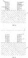
- Figure 1a shows a small portion of a device wafer, comprising a monocrystalline Si layer 1, into which a number of fins 2 have been produced by a known lithography and etch technique.
- the patterned mask 3 used for etching the fins is still present on top of the fins.
- the width of the fins may be in the order of 10 nm or less. Two groups of fins 2 are visible with a gap in between.
- the Si layer 1 may be the surface area of a bulk monocrystalline Si device wafer.
- the fins are produced on a monocrystalline upper layer of a multi-layer device wafer such as a silicon-on-insulator (SOI) wafer.
- SOI silicon-on-insulator
- the fabrication of a buried interconnect rail between the two groups of fins enables the processing of a power delivery network that is entirely located on the back side of an IC produced on the device wafer.
- the method of the present invention comprises the same initial steps for producing such buried interconnect rails.
- a shallow trench isolation (STI) oxide 4 is deposited on the wafer, as illustrated in Figure 1b .
- the STI is planarized by grinding and/or Chemical Mechanical polishing (CMP), stopping on the mask 3 on top of the fins 2 ( Fig. 1c ).
- CMP Chemical Mechanical polishing
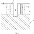
- a trench 5 is then produced between the two groups of fins, see Figure 1d , and a dielectric liner 6 is deposited on the sidewalls and the bottom of the trench 5, as well as on the upper surface of the wafer ( Fig. 1e ).
- the width of the trench 5 may be in the order of 20 to 100nm.
- the dielectric liner 6 may for example be applied by Atomic Layer Deposition (ALD) at a thickness in the order of 5 to a few tens of nanometers.
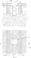
- a lithographic mask 10 is first produced on the wafer, as shown in Figure 1f .
- This may be a photoresist layer or any other suitable mask layer.
- the mask 10 covers the majority of the wafer surface except one or more areas 11 located above the trench 5. Only one such area is shown, but normally several areas of the trench as well as areas of other trenches across the device wafer are exposed in this way. The area is fully overlapping the trench in the direction transversal to the longitudinal direction of the trench, i.e. within this area 11 the trench 5 itself is fully exposed as well as portions of the wafer on either side of the trench.
- etch step is then performed in the exposed area, as illustrated in Figure 1g , whereby the liner 6 is removed on the bottom of the trench while maintaining the liner on the sidewalls.
- This may be done by a plasma-etch, as described for example in document EP3035369A1 .
- a self-aligned anisotropic etch step is then performed, removing the monocrystalline silicon down to a given depth, thereby forming a blind cavity 12.
- the depth of the cavity 12 is in the order of 400 to 600nm, starting from the bottom of the trench 5.
- the etch step for forming the cavity 12 is self-aligned with respect to the trench 5, as seen in the direction perpendicular to the trench, i.e.
- the cavity 12 has essentially the same width as the width of the trench 5 .
- the etch steps for removing the liner and for removing the silicon may be performed in the same reactor, but with different etch chemistries, suitable respectively for the removal of the liner 6 and of the silicon. Such chemistries and further details of the etch processes are known to the skilled person and therefore not described here in detail.
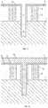
- a second dielectric liner 13 is now deposited on the bottom and sidewalls of the cavity 12. This is followed by the deposition of a seed layer and a barrier layer (not shown) on the liner 13 in the trench 5 and in the cavity 12. These steps are known as such in the art as process steps which precede the deposition of an electrically conductive material.
- This deposition step of conductive material 14 is then applied, as shown in Figure 1j .
- the conductive material may be highly doped silicon, or a metal such as tungsten or copper, applied by electrodeposition for example or by Chemical Vapor Deposition.
- the filled trench forms an elongated rail 15, having one or more micro-TSVs 16 extending downward from the rail, and having essentially the same width as the rail 15.
- microTSV is used herein, to indicate that the dimensions of these TSVs are smaller than what is usually termed a TSV in the terminology used in semiconductor processing.
- the dielectric liners 6 and 13 are present but have not been represented in Figure 2a in order not to complicate the drawing and in order not to reduce the visibility of the essential features. Also, gate strips and source/drain contacts have been produced on the fins, but these elements are equally not represented or not visible in the particular section shown in the drawings.
- the local interconnects 19 and local signal contacts 20 are embedded in a pre-metal dielectric layer 21. Via connections 22 connect the local signal contacts 20 to contact pads 23 in the first metallization layer of the back end of line stack 24.
- the liner 13 at the bottom of the microTSVs 16 is removed by chemical mechanical polishing, after the slow wet etch process.
- the CMP further removes any non-uniformities or possible protruding portions of the TSVs, resulting in a planarized semiconductor surface with exposed TSVs distributed across the surface.
- the CMP may be performed prior to depositing and patterning the passivation layer 30. Alternatively, CMP may be done after applying the passivation layer 30.
- the method of the invention may be applied on a multi-layer device wafer.
- the device wafer is a bulk silicon substrate 35, comprising a SiGe layer 36 and a monocrystalline Si layer 37 on its surface.
- the fins 2 have been produced by lithography and etching in the layer 37, using a mask 3, as in the above-described embodiment.
- the SiGe layer 36 may have a thickness of about 50 nm.
- the monocrystalline Si layer 37 (prior to formation of the fins) may be in the order of 500 nm to one micrometer thick.
- the blind cavities 12 for producing the microTSVs 16 may either be etched down to the SiGe layer 36, i.e.
- the thinning process ends with a wet etch process that is highly selective to the SiGe 36 and to the material of the microTSVs 16 , i.e. the Si of the bulk substrate 35 is removed but the SiGe layer 36 remains, as well as the microTSVs 16 (including the liner 13, not shown), as illustrated in Figure 5b .
- the presence of the SiGe layer 36 facilitates the thinning of the wafer to a precisely known thickness.
- the SiGe layer 36 is removed by a dry or wet etch process that is highly selective to Si, thereby ensuring that the remaining surface is Si with the exposed microTSVs 16 slightly protruding from the Si, as shown in Figure 5b .
Landscapes
- Internal Circuitry In Semiconductor Integrated Circuit Devices (AREA)
- Element Separation (AREA)
Abstract
Description
- The present invention is related to integrated circuit chips, hereafter abbreviated to ICs or IC chips, in particular to the aspect of the delivery of power to the active devices on the chip.
- Semiconductor processing for the fabrication of integrated circuit chips continues to evolve towards increasing device-density : higher numbers of active devices (mainly transistors) of ever decreasing device dimensions are placed on a given surface of semiconductor material. This has put a strain on the design and fabrication of the interconnects between the front end of line of the IC, consisting mainly of the active devices, and the contact terminals of the IC. Traditionally, all of these interconnects are incorporated in the back end of line of the IC : a stack of metallization layers on top of the front end of line and comprising layers of circuitry interconnected by vertical via connections. The power delivery network or PDN is specifically formed by conductors and vias connected to VDD/VSS terminals of the chip, for delivering power to the individual devices in the front end of line. The integration of this power delivery network in the back end of line has become particularly challenging because of the abovenamed increase in the device density.
- One known solution to this problem consists in the production of the majority of layers of the power delivery network on the back side of the IC instead of on the front side. These layers are thus not formed on top of the front end of line, but on the opposite side of the IC, i.e. on the backside of the semiconductor substrate onto which the active devices have been built.
- Document
EP3324436 describes an IC having the PDN that is integrally formed on the backside of the chip. This is achieved through the fabrication of buried interconnect rails embedded in the shallow trench isolation (STI) oxide, during front end of line processing of the IC, performed on a device wafer. After bonding of the device wafer to a landing wafer, the device wafer is thinned and Through Semiconductor Vias (TSV) are etched from the back side, through the thinned substrate. This process is however not scalable to the very small dimensions to which the semiconductor industry is evolving. Because of the wafer distortion induced during bonding, the buried rail pattern deformation within the wafer or within an IC is not linear and cannot be fully compensated during TSV patterning. This partial compensation does not allow a perfect alignment of backside TSVs to frontside buried interconnect rails all across the wafer. The residual overlay will also vary across the wafer, depending on the wafer bonder and bonding mechanism being used. Therefore, this backside approach is limited to relaxed pitches and critical dimensions (CD) of a few hundreds of nanometers. - The invention aims to provide a method of contacting buried interconnect rails that is scalable beyond the above-described limitations. This is achieved by the methods disclosed in the appended claims and summarized hereafter. The method of the invention is applicable in the production of an integrated circuit chip on a semiconductor device wafer, the IC comprising buried interconnect rails in the front end of line and a power delivery network (PDN) on the back side of the chip. The PDN is connected to the front side by micro-sized Through Semiconductor Via (TSV) connections through the thinned semiconductor wafer. Contrary to existing methods, the production of the TSVs is integrated in the FEOL process flow for fabricating the interconnect rails, with the TSVs being produced in a self-aligned manner relative to the interconnect rails. After flipping and bonding the device wafer to a landing wafer, the semiconductor layer onto which the active devices of the chip have been produced is thinned from the back side, and the TSVs are exposed, so that they may be contacted by the PDN produced on the back side. The self-aligned manner of producing the TSVs enables scaling down the process towards smaller dimensions without losing accurate positioning of the TSVs.
- The invention is in particular related to a method for producing an integrated circuit chip comprising the steps of :
- Providing a device substrate comprising a semiconductor material at least on its upper surface, and producing a front end of line (FEOL) portion of the chip on the semiconductor material of the device substrate, wherein the FEOL portion comprises active devices and interconnect rails, the interconnect rails being at least partially embedded in a shallow trench isolation (STI) dielectric layer,
- Producing a back end of line (BEOL) portion on the FEOL portion,
- Bonding the device substrate to a landing substrate (26), with the surface of the BEOL portion being bonded to a surface of the landing substrate, and thereafter :
- Thinning the device substrate from the back side,
- Producing a power delivery network (PDN) on the thinned backside of the device substrate, wherein the PDN is connected to the interconnect rails by a plurality of through semiconductor vias (TSV) which are isolated from the semiconductor material of the device substrate by a dielectric liner,
- the TSVs are formed during the production of the FEOL portion on the device substrate, the TSVs extending into the semiconductor material of the device substrate and being formed in a self-aligned manner with respect to the interconnect rails, the TSVs being self-aligned to the rails in the direction perpendicular to the rails, with the liner isolating the TSVs laterally and on the bottom of the TSVs,
- the thinning step includes thinning the semiconductor material of the device substrate until the liner at the bottom of the TSVs is exposed,
- the liner is subsequently removed from the bottom of the TSVs so as to allow the PDN to contact the TSVs.
- According to an embodiment, the production of the interconnect rails and the TSVs includes the steps of:
- Producing a trench through the STI dielectric and extending into the semiconductor material of the device substrate,
- Providing a first dielectric liner on the bottom and the sidewalls of the trench, and thereafter :
- Providing a mask that defines at least one local open area extending across the longitudinal direction of the trench and on both sides of the trench, ,
- Removing the liner from the bottom of the trench in said open area, and thereafter :
- Etching a blind cavity extending underneath the trench, by a self-aligned etch process in said open area, the etch process being self-aligned to the trench in the direction perpendicular to the longitudinal direction of the trench,
- Providing a second dielectric liner on the bottom and the sidewalls of the blind cavity, and thereafter:
- Filling the blind cavity and the trench with an electrically conducting material, so as to create a rail having one of said TSVs extending locally and in a self-aligned manner from the bottom of the rail.
- According to an embodiment, the device substrate comprises a base substrate, an etch stop layer on top of the base substrate, and said semiconductor layer on top of the etch stop layer, and wherein the thinning step comprises grinding and etching the base substrate from the back side, ending with an etch process that is stopped by the etch stop layer.
- The base substrate may be a silicon substrate, the etch stop layer may be a SiGe layer and the semiconductor layer may be a monocrystalline silicon layer.
- The device substrate may be a silicon-on-insulator substrate, comprising a silicon base substrate, an insulator layer acting as the etch stop layer, and a monocrystalline silicon layer on the insulator layer.
- According to an embodiment, the device substrate is a monocrystalline substrate wherein the etch stop layer is formed by dopant elements implanted into the substrate and forming a layer at a given implant depth.
- According to an embodiment, the etch stop layer furthermore stops the self-aligned etch process, so that the bottom of the blind cavity is formed by the etch stop layer.
- According to another embodiment, the etch stop layer does not stop the self-aligned etch process, and said self-aligned etch process is continued until the bottom of the blind cavity protrudes through the etch stop layer.
- The method of the invention may further comprise the following steps, after the thinning step :
- If applicable, removing the etch stop layer,
- depositing a passivation layer,
- opening the passivation layer at the location of the TSVs by lithography and by an etch process,
- Alternatively, the liner may be removed from the bottom of the TSVs by a chemical mechanical polishing (CMP) step. In the latter case, the TSVs including the liner may protrude from the thinned back side of the device substrate after the thinning step, and a passivation layer may be deposited on the thinned back side and on the protruding TSVs, followed by said CMP step, wherein the CMP step planarizes the surface of the passivation layer, thereby removing the liner from the bottom of the TSVs.
- The enclosed figures are illustrating the main features of the invention. They are not drawn to scale and should not be regarded as technical drawings of real structures.
-
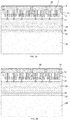
Figures 1a to 1k illustrate the fabrication of a microTSV extending from a buried interconnect rail by a self-aligned etch process, in accordance with the method of the invention applied on a silicon device wafer. The term microTSV is used herein, to indicate that the dimensions of these TSVs are smaller than what is usually termed a TSV in the terminology used in semiconductor processing. -
Figures 2a to 2f illustrate the steps of the method according to the invention, executed after bonding the device wafer to a landing wafer. -
Figure 3 illustrates a device wafer applicable in the method of the invention, comprising a silicon layer on top of a SiGe etch stop layer. -
Figure 4a illustrates that the SiGe layer may stop the self-aligned etching of the blind cavity needed to produce a microTSV.Figure 4b illustrates an alternative embodiment wherein the SiGe layer does not stop this etching process and wherein the blind cavity protrudes slightly through the SiGe layer. -
Figures 5a to 5c illustrate the etch stop function of the SiGe layer in the step of thinning the device wafer in accordance with the method of the invention. - In the following detailed description, an embodiment of the method of the invention is described for the case of a CMOS layout of finFET transistors produced on a semiconductor device wafer. However, the invention is not limited to this particular application field.
Figure 1a shows a small portion of a device wafer, comprising amonocrystalline Si layer 1, into which a number offins 2 have been produced by a known lithography and etch technique. The patternedmask 3 used for etching the fins is still present on top of the fins. The width of the fins may be in the order of 10 nm or less. Two groups offins 2 are visible with a gap in between. This layout is typically used for producing pMOS and nMOS transistors on the two groups of fins respectively, as described for example inEP3324436 . TheSi layer 1 may be the surface area of a bulk monocrystalline Si device wafer. Alternatively and as will be described in more detail further in this text, the fins are produced on a monocrystalline upper layer of a multi-layer device wafer such as a silicon-on-insulator (SOI) wafer. - As equally disclosed in
EP3324436 , the fabrication of a buried interconnect rail between the two groups of fins enables the processing of a power delivery network that is entirely located on the back side of an IC produced on the device wafer. The method of the present invention comprises the same initial steps for producing such buried interconnect rails. First, a shallow trench isolation (STI)oxide 4 is deposited on the wafer, as illustrated inFigure 1b . The STI is planarized by grinding and/or Chemical Mechanical polishing (CMP), stopping on themask 3 on top of the fins 2 (Fig. 1c ). These process steps are well-known and may be executed according to well-established techniques and process parameters. By lithography and etching, atrench 5 is then produced between the two groups of fins, seeFigure 1d , and adielectric liner 6 is deposited on the sidewalls and the bottom of thetrench 5, as well as on the upper surface of the wafer (Fig. 1e ). The width of thetrench 5 may be in the order of 20 to 100nm. Thedielectric liner 6 may for example be applied by Atomic Layer Deposition (ALD) at a thickness in the order of 5 to a few tens of nanometers. These steps are also included in the method ofEP3324436 . - Contrary to the method of
EP3324436 however, thetrench 5 is not yet filled with an electrically conductive material at this point. Alithographic mask 10 is first produced on the wafer, as shown inFigure 1f . This may be a photoresist layer or any other suitable mask layer. As seen in the plane view inFigure 1f , themask 10 covers the majority of the wafer surface except one ormore areas 11 located above thetrench 5. Only one such area is shown, but normally several areas of the trench as well as areas of other trenches across the device wafer are exposed in this way. The area is fully overlapping the trench in the direction transversal to the longitudinal direction of the trench, i.e. within thisarea 11 thetrench 5 itself is fully exposed as well as portions of the wafer on either side of the trench. - An etch step is then performed in the exposed area, as illustrated in
Figure 1g , whereby theliner 6 is removed on the bottom of the trench while maintaining the liner on the sidewalls. This may be done by a plasma-etch, as described for example in documentEP3035369A1 . As shown inFigure 1h , a self-aligned anisotropic etch step is then performed, removing the monocrystalline silicon down to a given depth, thereby forming ablind cavity 12. Preferably the depth of thecavity 12 is in the order of 400 to 600nm, starting from the bottom of thetrench 5. The etch step for forming thecavity 12 is self-aligned with respect to thetrench 5, as seen in the direction perpendicular to the trench, i.e. thecavity 12 has essentially the same width as the width of thetrench 5 . The etch steps for removing the liner and for removing the silicon may be performed in the same reactor, but with different etch chemistries, suitable respectively for the removal of theliner 6 and of the silicon. Such chemistries and further details of the etch processes are known to the skilled person and therefore not described here in detail. - The result is an
elongated trench 5 with the localblind cavity 12 at the location of theopen area 11 defined by themask 10. As seen inFigure 1i , asecond dielectric liner 13 is now deposited on the bottom and sidewalls of thecavity 12. This is followed by the deposition of a seed layer and a barrier layer (not shown) on theliner 13 in thetrench 5 and in thecavity 12. These steps are known as such in the art as process steps which precede the deposition of an electrically conductive material. This deposition step ofconductive material 14 is then applied, as shown inFigure 1j . The conductive material may be highly doped silicon, or a metal such as tungsten or copper, applied by electrodeposition for example or by Chemical Vapor Deposition. - After planarization of the
conductive material 14 and theliners mask portions 3 on top of thefins 2, the structure illustrated inFigure 1k is obtained. The filled trench forms anelongated rail 15, having one or more micro-TSVs 16 extending downward from the rail, and having essentially the same width as therail 15. The term microTSV is used herein, to indicate that the dimensions of these TSVs are smaller than what is usually termed a TSV in the terminology used in semiconductor processing. - The method for further processing the buried
rail 15 and connecting it to thefins 2 involves etching back the conductive material of the rail and producing local interconnects between the rail on the one hand and active devices produced on the fins on the other hand. Back end of line processing is then performed on top of the fins to produce interconnects between the multiple active devices in the front end of line. This is fully described inEP3324436 and may be executed in the same manner in the method of the invention. - The result is a device wafer as shown in the upper portion of
Figure 2a , illustrating an area of the wafer comprising multiple groups offins 2 embedded in theSTI oxide 4, with buriedrails 15 in between the groups, and themicroTSVs 16 extending downward from the bottom of therails 15. MicroTSVs are shown to extend from every rail in the cross-section shown inFigure 2a . This is not a requirement and in reality the TSVs will be distributed across the surface of the wafer in accordance with a predefined pattern, that may depend on the design of the PDN, as described also inEP3324436 . - It is seen furthermore that the height of the
rails 15 has been reduced, after whichlocal interconnects 19 andlocal signal contacts 20 have been produced in accordance with the method described inEP3324436 . Thedielectric liners Figure 2a in order not to complicate the drawing and in order not to reduce the visibility of the essential features. Also, gate strips and source/drain contacts have been produced on the fins, but these elements are equally not represented or not visible in the particular section shown in the drawings. Thelocal interconnects 19 andlocal signal contacts 20 are embedded in a pre-metaldielectric layer 21. Viaconnections 22 connect thelocal signal contacts 20 to contactpads 23 in the first metallization layer of the back end ofline stack 24. Thelocal interconnects 19 connect source and drain areas of a number of active devices to the buried rails 15. Adielectric bonding layer 25 is furthermore applied on top of theBEOL stack 24. The lower portion ofFigure 2a shows alanding wafer 26, equally comprising adielectric bonding layer 27. These bonding layers 25 and 27 may be silicon oxide layers or SiCN layers, or any other layers applicable in direct bonding, i.e. bonding by directly contacting dielectric bonding layers, usually oxide layers which undergo chemical bonding, under the influence of increased contact pressure and/or increased temperature. Bonding of the device wafer to the landing wafer takes place by such known direct bonding techniques, thus obtaining a wafer assembly as shown inFigure 2b . The landingwafer 26 may be a temporary carrier wafer, or another device wafer, or any other suitable substrate to which the device wafer may be attached. - Thinning of the
device wafer 1 is then performed by a series of thinning steps, including grinding and wet or dry etching, for example beginning with a grinding step, reducing the wafer to a thickness of 50 micrometers, CMP down to 49 micrometers, fast dry etching down to about 10 micrometers, and slow wet etching down to 1 micrometer or less. According to one embodiment, the slow wet etching continues until theliner 13 at the bottom of themicroTSVs 16 is exposed, as illustrated inFigure 2c . A slight overetch may be allowed, resulting in the TSVs 16 (including the liner 13) protruding from the thinned surface.Figure 2c however shows the case wherein the thinned surface obtained by the slow etch process is essentially planar. Apassivation layer 30 is then deposited, seeFigure 2d . Thepassivation layer 30 may be formed of SiON, SiCN or SICO for example. The thickness of thepassivation layer 30 may for example be about 50 nm. Thepassivation layer 30 is opened by lithography and by etching. This same etching process or a subsequent etching process removes theliner 13 at the bottom of the microTSVs, thereby exposing themicroTSVs 16 as such (Fig. 2e ). This is followed by standard damascene type processing, for producing afirst metallization layer 31 of the power delivery network (Fig. 2f ). Additional metallization layers may be produced in accordance with the method described inEP3324436 to arrive at a backside PDN having the same connectivity as described in said document. - According to another embodiment, the
liner 13 at the bottom of themicroTSVs 16 is removed by chemical mechanical polishing, after the slow wet etch process. Preferably the CMP further removes any non-uniformities or possible protruding portions of the TSVs, resulting in a planarized semiconductor surface with exposed TSVs distributed across the surface. The CMP may be performed prior to depositing and patterning thepassivation layer 30. Alternatively, CMP may be done after applying thepassivation layer 30. In the latter case, the slow wet etch process is applied so as to overetch thesemiconductor material 1 of the device wafer, resulting in the microTSVs 16 (including the liner 13) protruding outward from the thinneddevice wafer 1 at the end of the slow wet etch process. Thepassivation layer 30 is then applied on the topography defined by the protruding microTSVs, and the passivation layer is planarized by CMP, until theliner 13 is removed from the TSVs, as well as non-uniformities of the TSVs themselves, so as to obtain the planarized surface of thepassivation layer 30, with exposed TSVs distributed across said surface. Standard process steps for producing the PDN are then performed. - The advantage of the method according to the invention in comparison with
EP3324436 is that the method includes self-aligned formation of themicroTSVs 16 prior to the step of bonding the device wafer to a landing wafer and thinning the device wafer. The self-aligned manner, relative to therails 15, in which themicroTSVs 16 are formed allows perfect alignment of these microTSVs to the buried rails 15, regardless of the dimensions of said rails and TSVs. - As stated above, the method of the invention may be applied on a multi-layer device wafer. According to a preferred embodiment illustrated in
Figure 3 , the device wafer is abulk silicon substrate 35, comprising aSiGe layer 36 and amonocrystalline Si layer 37 on its surface. Thefins 2 have been produced by lithography and etching in thelayer 37, using amask 3, as in the above-described embodiment. TheSiGe layer 36 may have a thickness of about 50 nm. The monocrystalline Si layer 37 (prior to formation of the fins) may be in the order of 500 nm to one micrometer thick. Theblind cavities 12 for producing themicroTSVs 16 may either be etched down to theSiGe layer 36, i.e. the etch process may be selective to SiGe and thus stop on the SiGe layer, as illustrated inFigure 4a . Alternatively, the etch process may be non-selective to SiGe and continue over a limited distance through theSiGe layer 36, as illustrated inFigure 4b . - The main function of the
SiGe layer 36 is to serve as an etch stop layer during the wet etch process applied for thinning the device wafer after bonding the wafer to the landing wafer. This is illustrated inFigures 5a to 5c for the case ofFigure 4b , i.e. themicroTSVs 16 protrude slightly through theSiGe layer 36.Figure 5a is the situation after bonding of the device wafer to thelanding wafer 26, by direct bonding between the dielectric bonding layers 25 and 27 as described above. Thinning of the device wafer is performed by the series of thinning steps as equally described above, i.e. grinding and dry etch. Now the thinning process ends with a wet etch process that is highly selective to theSiGe 36 and to the material of themicroTSVs 16 , i.e. the Si of thebulk substrate 35 is removed but theSiGe layer 36 remains, as well as the microTSVs 16 (including theliner 13, not shown), as illustrated inFigure 5b . The presence of theSiGe layer 36 facilitates the thinning of the wafer to a precisely known thickness. After the wet etch process, theSiGe layer 36 is removed by a dry or wet etch process that is highly selective to Si, thereby ensuring that the remaining surface is Si with the exposedmicroTSVs 16 slightly protruding from the Si, as shown inFigure 5b . After this, the method is continued in the same way as described in relation toFigures 2d to 2f (removal ofliner 13, deposition ofpassivation 30, etc). Theliner 13 may be removed by etching or by CMP, as equally described above. When the microTSVs are protruding from the Si, the above-described steps may be applied of depositing thepassivation layer 30 on the topography defined by the protruding microTSVs, followed by a CMP step, to planarize the surface of the passivation layer, thereby removing the liner from the microTSVs. - According to a preferred embodiment, the
SiGe layer 36 comprises between 20% and 30% Ge. Within this range, the selectivity of the wet etch process to the SiGe is sufficiently high, while the properties of themonocrystalline Si layer 37 are acceptable in terms of the strain and the smoothness of this layer. - An alternative multilayer structure that is suitable for the invention is a silicon-on-insulator (SOI) substrate, known in the art. The insulator layer (normally a silicon oxide layer) in the SOI may play the same part as the SiGe layer in the previous embodiment. According to yet another embodiment, the method is applied on a bulk monocrystalline semiconductor substrate that has been provided with dopant elements by dopant implantation, in such a manner that the dopants form a layer at a depth comparable to the depth of the SiGe layer described above. The dopant layer performs the same function as the SiGe layer described above, i.e. forming an etch stop layer at least for the wet etching of the semiconductor material above the etch stop layer at the end of the thinning process.
- As stated, the method is not limited to the application on fin-shaped devices, but it is applicable to the production of buried interconnect rails amid any design and type of active devices on an IC.
- While the invention has been illustrated and described in detail in the drawings and foregoing description, such illustration and description are to be considered illustrative or exemplary and not restrictive. Other variations to the disclosed embodiments can be understood and effected by those skilled in the art in practicing the claimed invention, from a study of the drawings, the disclosure and the appended claims. In the claims, the word "comprising" does not exclude other elements or steps, and the indefinite article "a" or "an" does not exclude a plurality. The mere fact that certain measures are recited in mutually different dependent claims does not indicate that a combination of these measures cannot be used to advantage. Any reference signs in the claims should not be construed as limiting the scope.
Claims (11)
- A method for producing an integrated circuit chip comprising the steps of :- Providing a device substrate (1;35,36,37) comprising a semiconductor material (1,37) at least on its upper surface, and producing a front end of line (FEOL) portion of the chip on the semiconductor material of the device substrate, wherein the FEOL portion comprises active devices and interconnect rails (15), the interconnect rails being at least partially embedded in a shallow trench isolation (STI) dielectric layer (4),- Producing a back end of line (BEOL) portion (24) on the FEOL portion,- Bonding the device substrate to a landing substrate (26), with the surface of the BEOL portion (24) being bonded to a surface of the landing substrate (26), and thereafter:- Thinning the device substrate from the back side,- Producing a power delivery network (PDN) on the thinned backside of the device substrate, wherein the PDN is connected to the interconnect rails (15) by a plurality of through semiconductor vias (TSV) (16) which are isolated from the semiconductor material of the device substrate by a dielectric liner (13),wherein :- the TSVs (16) are formed during the production of the FEOL portion on the device substrate, the TSVs extending into the semiconductor material of the device substrate and being formed in a self-aligned manner with respect to the interconnect rails (15), the TSVs being self-aligned to the rails in the direction perpendicular to the rails, with the liner (13) isolating the TSVs laterally and on the bottom of the TSVs,- the thinning step includes thinning the semiconductor material of the device substrate until the liner (13) at the bottom of the TSVs is exposed,- the liner (13) is subsequently removed from the bottom of the TSVs so as to allow the PDN to contact the TSVs.
- The method according to claim 1, wherein the production of the interconnect rails (15) and the TSVs (16) includes the steps of:- Producing a trench (5) through the STI dielectric (4) and extending into the semiconductor material of the device substrate,- Providing a first dielectric liner (6) on the bottom and the sidewalls of the trench (5), and thereafter:- Providing a mask (10) that defines at least one local open area (11) extending across the longitudinal direction of the trench (5) and on both sides of the trench, ,- Removing the liner (6) from the bottom of the trench in said open area (11), and thereafter:- Etching a blind cavity (12) extending underneath the trench, by a self-aligned etch process in said open area (11), the etch process being self-aligned to the trench (5) in the direction perpendicular to the longitudinal direction of the trench,- Providing a second dielectric liner (13) on the bottom and the sidewalls of the blind cavity (12), and thereafter :- Filling the blind cavity (12) and the trench (5) with an electrically conducting material (14), so as to create a rail (15) having one of said TSVs (16) extending locally and in a self-aligned manner from the bottom of the rail (15).
- The method according to claim 1 or 2, wherein the device substrate comprises a base substrate (35), an etch stop layer (36) on top of the base substrate, and said semiconductor layer (37) on top of the etch stop layer, and wherein the thinning step comprises grinding and etching the base substrate from the back side, ending with an etch process that is stopped by the etch stop layer (36).
- The method according to claim 3, wherein the base substrate (35) is a silicon substrate, the etch stop layer (36) is a SiGe layer and the semiconductor layer (37) is a monocrystalline silicon layer.
- The method according to claim 3, wherein the device substrate is a silicon-on-insulator substrate, comprising a silicon base substrate, an insulator layer acting as the etch stop layer, and a monocrystalline silicon layer on the insulator layer.
- The method according to claim 3, wherein the device substrate is a monocrystalline substrate and wherein the etch stop layer is formed by dopant elements implanted into the substrate and forming a layer at a given implant depth.
- The method according to any one of claims 3 to 6, wherein the etch stop layer (36) furthermore stops the self-aligned etch process, so that the bottom of the blind cavity (12) is formed by the etch stop layer (36).
- The method according to any one of claims 3 to 6, wherein the etch stop layer (36) does not stop the self-aligned etch process, and wherein said self-aligned etch process is continued until the bottom of the blind cavity (12) protrudes through the etch stop layer.
- The method according to any one of the preceding claims, further comprising the following steps, after the thinning step :• If applicable, removing the etch stop layer (36),• depositing a passivation layer (30),• opening the passivation layer at the location of the TSVs (16) by lithography and by an etch process,and wherein the step of removing the liner (13) from the bottom of the TSVs so as to allow the PDN to contact the TSVs is performed by said etch process for opening the passivation layer (30), or by a subsequent etch process.
- The method according to any one of claims 1 to 8, wherein the liner (13) is removed from the bottom of the TSVs (16) by a chemical mechanical polishing (CMP) step.
- The method according to claim 10, wherein the TSVs (16) including the liner (13), protrude from the thinned back side of the device substrate after the thinning step, and wherein a passivation layer (30) is deposited on the thinned back side and on the protruding TSVs, followed by said CMP step, wherein the CMP step planarizes the surface of the passivation layer (30), thereby removing the liner (13) from the bottom of the TSVs.
Priority Applications (2)
| Application Number | Priority Date | Filing Date | Title |
|---|---|---|---|
| EP18205606.9A EP3651188B1 (en) | 2018-11-12 | 2018-11-12 | A method for contacting a buried interconnect rail from the back side of an ic |
| US16/675,080 US10985057B2 (en) | 2018-11-12 | 2019-11-05 | Method for contacting a buried interconnect rail of an integrated circuit chip from the back side of the IC |
Applications Claiming Priority (1)
| Application Number | Priority Date | Filing Date | Title |
|---|---|---|---|
| EP18205606.9A EP3651188B1 (en) | 2018-11-12 | 2018-11-12 | A method for contacting a buried interconnect rail from the back side of an ic |
Publications (2)
| Publication Number | Publication Date |
|---|---|
| EP3651188A1 true EP3651188A1 (en) | 2020-05-13 |
| EP3651188B1 EP3651188B1 (en) | 2021-05-19 |
Family
ID=64277540
Family Applications (1)
| Application Number | Title | Priority Date | Filing Date |
|---|---|---|---|
| EP18205606.9A Active EP3651188B1 (en) | 2018-11-12 | 2018-11-12 | A method for contacting a buried interconnect rail from the back side of an ic |
Country Status (2)
| Country | Link |
|---|---|
| US (1) | US10985057B2 (en) |
| EP (1) | EP3651188B1 (en) |
Cited By (5)
| Publication number | Priority date | Publication date | Assignee | Title |
|---|---|---|---|---|
| EP3944298A1 (en) * | 2020-07-22 | 2022-01-26 | Taiwan Semiconductor Manufacturing Company, Ltd. | Semiconductor device with backside spacer and methods of forming the same |
| KR20220056668A (en) * | 2020-10-28 | 2022-05-06 | 삼성전자주식회사 | integrated circuit semiconductor device |
| EP4152381A1 (en) | 2021-09-16 | 2023-03-22 | Imec VZW | An integrated circuit chip comprising back-side power delivery tracks |
| WO2023066797A1 (en) * | 2021-10-22 | 2023-04-27 | International Business Machines Corporation | Early backside first power delivery network |
| TWI899257B (en) * | 2020-11-03 | 2025-10-01 | 南韓商三星電子股份有限公司 | Integrated circuit chip having bs-pdn structure |
Families Citing this family (22)
| Publication number | Priority date | Publication date | Assignee | Title |
|---|---|---|---|---|
| US10550405B2 (en) | 2017-03-15 | 2020-02-04 | The University Of North Carolina At Chapel Hill | Rational polyploid adeno-associated virus vectors and methods of making and using the same |
| CN113517274B (en) * | 2020-07-24 | 2025-03-25 | 台湾积体电路制造股份有限公司 | Semiconductor device and method for forming the same |
| KR102821727B1 (en) * | 2020-08-03 | 2025-06-19 | 삼성전자주식회사 | Semiconductor device and semiconductor package |
| KR102864985B1 (en) * | 2020-12-31 | 2025-09-25 | 삼성전자주식회사 | Semiconductor device |
| EP4044218B1 (en) | 2021-02-11 | 2024-01-17 | Imec VZW | Methods for producing a through semiconductor via connection |
| US12106969B2 (en) | 2021-03-18 | 2024-10-01 | International Business Machines Corporation | Substrate thinning for a backside power distribution network |
| US11881455B2 (en) | 2021-05-20 | 2024-01-23 | Samsung Electronics Co., Ltd. | Through silicon buried power rail implemented backside power distribution network semiconductor architecture and method of manufacturing the same |
| US11817394B2 (en) | 2021-10-11 | 2023-11-14 | International Business Machines Corporation | Semiconductor circuit power delivery |
| EP4170706A1 (en) | 2021-10-20 | 2023-04-26 | Imec VZW | A method for producing an integrated circuit chip comprising a back-side power delivery network |
| US12230571B2 (en) | 2021-11-23 | 2025-02-18 | Samsung Electronics Co., Ltd. | Integrated circuit devices including a power rail and methods of forming the same |
| EP4187581A1 (en) | 2021-11-26 | 2023-05-31 | Imec VZW | An interconnect structure of a semiconductor component and methods for producing said structure |
| US12444653B2 (en) | 2021-12-08 | 2025-10-14 | International Business Machines Corporation | Buried power rail at tight cell-to-cell space |
| US12279452B2 (en) | 2021-12-15 | 2025-04-15 | International Business Machines Corporation | Stacked complementary transistor structure for three-dimensional integration |
| US12604719B2 (en) | 2022-02-04 | 2026-04-14 | Samsung Electronics Co., Ltd. | Semiconductor device having a through-via structure electrically connected to a contact structure |
| US12131996B2 (en) * | 2022-03-28 | 2024-10-29 | Samsung Electronics Co., Ltd. | Stacked device with backside power distribution network and method of manufacturing the same |
| KR20230141220A (en) | 2022-03-31 | 2023-10-10 | 삼성전자주식회사 | Semiconductor device |
| US12451431B2 (en) | 2022-05-02 | 2025-10-21 | International Business Machines Corporation | Stacked semiconductor devices with topside and backside interconnect wiring |
| US12550712B2 (en) | 2022-05-24 | 2026-02-10 | International Business Machines Corporation | Bulk substrate backside power rail |
| KR102945104B1 (en) * | 2022-08-04 | 2026-03-26 | 삼성전자주식회사 | Semiconductor device |
| US12550785B2 (en) | 2022-08-24 | 2026-02-10 | International Business Machines Corporation | Separated input/output (I/O) and shared power terminals for a carrier wafer with a built-in device for bonding with another device wafer |
| US20240297167A1 (en) * | 2023-03-01 | 2024-09-05 | International Business Machines Corporation | Self-aligned backside interconnect structures |
| US12550390B2 (en) | 2023-07-13 | 2026-02-10 | International Business Machines Corporation | Trench isolation for backside contact formation |
Citations (5)
| Publication number | Priority date | Publication date | Assignee | Title |
|---|---|---|---|---|
| JP2005032839A (en) * | 2003-07-08 | 2005-02-03 | Toshiba Microelectronics Corp | Semiconductor integrated circuit and master chip |
| US20120199916A1 (en) * | 2011-02-03 | 2012-08-09 | Elpida Memory, Inc | Semiconductor device |
| US20150162295A1 (en) * | 2013-12-11 | 2015-06-11 | Taiwan Semiconductor Manufacturing Co., Ltd. | Connecting techniques for stacked cmos devices |
| EP3035369A1 (en) | 2014-12-18 | 2016-06-22 | IMEC vzw | Plasma treatment method |
| EP3324436A1 (en) | 2016-11-21 | 2018-05-23 | IMEC vzw | An integrated circuit chip with power delivery network on the backside of the chip |
Family Cites Families (5)
| Publication number | Priority date | Publication date | Assignee | Title |
|---|---|---|---|---|
| US20110260248A1 (en) * | 2010-04-27 | 2011-10-27 | Peter Smeys | SOI Wafer and Method of Forming the SOI Wafer with Through the Wafer Contacts and Trench Based Interconnect Structures that Electrically Connect the Through the Wafer Contacts |
| KR101840846B1 (en) * | 2012-02-15 | 2018-03-21 | 삼성전자주식회사 | Semicoductor devices having through vias and methods for fabricating the same |
| KR101934045B1 (en) * | 2012-03-22 | 2019-01-02 | 삼성전자주식회사 | Semiconductor devices and methods of manufacturing a semiconductor device |
| KR102079283B1 (en) * | 2013-10-15 | 2020-02-19 | 삼성전자 주식회사 | Integrated circuit device having through-silicon via structure and method of manufacturing the same |
| US9887123B2 (en) * | 2014-10-24 | 2018-02-06 | Newport Fab, Llc | Structure having isolated deep substrate vias with decreased pitch and increased aspect ratio and related method |
-
2018
- 2018-11-12 EP EP18205606.9A patent/EP3651188B1/en active Active
-
2019
- 2019-11-05 US US16/675,080 patent/US10985057B2/en active Active
Patent Citations (5)
| Publication number | Priority date | Publication date | Assignee | Title |
|---|---|---|---|---|
| JP2005032839A (en) * | 2003-07-08 | 2005-02-03 | Toshiba Microelectronics Corp | Semiconductor integrated circuit and master chip |
| US20120199916A1 (en) * | 2011-02-03 | 2012-08-09 | Elpida Memory, Inc | Semiconductor device |
| US20150162295A1 (en) * | 2013-12-11 | 2015-06-11 | Taiwan Semiconductor Manufacturing Co., Ltd. | Connecting techniques for stacked cmos devices |
| EP3035369A1 (en) | 2014-12-18 | 2016-06-22 | IMEC vzw | Plasma treatment method |
| EP3324436A1 (en) | 2016-11-21 | 2018-05-23 | IMEC vzw | An integrated circuit chip with power delivery network on the backside of the chip |
Cited By (7)
| Publication number | Priority date | Publication date | Assignee | Title |
|---|---|---|---|---|
| EP3944298A1 (en) * | 2020-07-22 | 2022-01-26 | Taiwan Semiconductor Manufacturing Company, Ltd. | Semiconductor device with backside spacer and methods of forming the same |
| KR20220056668A (en) * | 2020-10-28 | 2022-05-06 | 삼성전자주식회사 | integrated circuit semiconductor device |
| TWI899257B (en) * | 2020-11-03 | 2025-10-01 | 南韓商三星電子股份有限公司 | Integrated circuit chip having bs-pdn structure |
| EP4152381A1 (en) | 2021-09-16 | 2023-03-22 | Imec VZW | An integrated circuit chip comprising back-side power delivery tracks |
| US12557634B2 (en) | 2021-09-16 | 2026-02-17 | Imec Vzw | Integrated circuit chip including back side power delivery tracks |
| WO2023066797A1 (en) * | 2021-10-22 | 2023-04-27 | International Business Machines Corporation | Early backside first power delivery network |
| JP2023063252A (en) * | 2021-10-22 | 2023-05-09 | インターナショナル・ビジネス・マシーンズ・コーポレーション | Semiconductor structure, method (early backside primary power supply network) |
Also Published As
| Publication number | Publication date |
|---|---|
| EP3651188B1 (en) | 2021-05-19 |
| US10985057B2 (en) | 2021-04-20 |
| US20200152508A1 (en) | 2020-05-14 |
Similar Documents
| Publication | Publication Date | Title |
|---|---|---|
| US10985057B2 (en) | Method for contacting a buried interconnect rail of an integrated circuit chip from the back side of the IC | |
| EP3324436B1 (en) | An integrated circuit chip with power delivery network on the backside of the chip | |
| US6495454B2 (en) | Substrate interconnect for power distribution on integrated circuits | |
| US8563396B2 (en) | 3D integration method using SOI substrates and structures produced thereby | |
| US7741205B2 (en) | Integrated circuit having a top side wafer contact and a method of manufacture therefor | |
| US20110304057A1 (en) | Semiconductor device and manufacturing method of the device | |
| KR20120002499A (en) | Semiconductor device including through hole vias with stress relief mechanism | |
| US12494424B2 (en) | Interconnect structure of a semiconductor component and methods for producing the structure | |
| US20150061085A1 (en) | Package interconnects | |
| JP2014107304A (en) | Semiconductor device and manufacturing method of the same | |
| US20230253322A1 (en) | Nano-tsv landing over buried power rail | |
| TW201841311A (en) | Segmented guard ring and wafer edge seal | |
| US20250300021A1 (en) | Dual-side power rail design and method of making same | |
| US20260113986A1 (en) | Semiconductor structure having stacked gates and method of manufacture thereof | |
| US12538779B2 (en) | Method for producing a buried interconnect rail of an integrated circuit chip | |
| EP3929971A1 (en) | A method for inducing stress in semiconductor devices | |
| US20220270924A1 (en) | Method for producing a through semiconductor via connection | |
| TWI680533B (en) | Devices and methods of forming thereof by post single layer transfer fabrication of device isolation structures | |
| US12362236B2 (en) | Method of producing an integrated circuit chip including a back-side power delivery network | |
| KR100418332B1 (en) | Semiconductor device and method of manufacturing the same | |
| EP4152381B1 (en) | An integrated circuit chip comprising back-side power delivery tracks | |
| US11387167B2 (en) | Semiconductor structure and manufacturing method for the same | |
| US20250118564A1 (en) | Method for Thinning a Semiconductor Substrate | |
| EP4287246A1 (en) | A method for producing an interconnect rail for contacting a semiconductor device from the back side |
Legal Events
| Date | Code | Title | Description |
|---|---|---|---|
| PUAI | Public reference made under article 153(3) epc to a published international application that has entered the european phase |
Free format text: ORIGINAL CODE: 0009012 |
|
| STAA | Information on the status of an ep patent application or granted ep patent |
Free format text: STATUS: THE APPLICATION HAS BEEN PUBLISHED |
|
| AK | Designated contracting states |
Kind code of ref document: A1 Designated state(s): AL AT BE BG CH CY CZ DE DK EE ES FI FR GB GR HR HU IE IS IT LI LT LU LV MC MK MT NL NO PL PT RO RS SE SI SK SM TR |
|
| AX | Request for extension of the european patent |
Extension state: BA ME |
|
| STAA | Information on the status of an ep patent application or granted ep patent |
Free format text: STATUS: REQUEST FOR EXAMINATION WAS MADE |
|
| GRAP | Despatch of communication of intention to grant a patent |
Free format text: ORIGINAL CODE: EPIDOSNIGR1 |
|
| STAA | Information on the status of an ep patent application or granted ep patent |
Free format text: STATUS: GRANT OF PATENT IS INTENDED |
|
| 17P | Request for examination filed |
Effective date: 20201109 |
|
| RBV | Designated contracting states (corrected) |
Designated state(s): AL AT BE BG CH CY CZ DE DK EE ES FI FR GB GR HR HU IE IS IT LI LT LU LV MC MK MT NL NO PL PT RO RS SE SI SK SM TR |
|
| RIC1 | Information provided on ipc code assigned before grant |
Ipc: H01L 23/528 20060101ALI20201125BHEP Ipc: H01L 21/768 20060101AFI20201125BHEP Ipc: H01L 21/74 20060101ALI20201125BHEP Ipc: H01L 23/48 20060101ALI20201125BHEP |
|
| INTG | Intention to grant announced |
Effective date: 20201216 |
|
| GRAS | Grant fee paid |
Free format text: ORIGINAL CODE: EPIDOSNIGR3 |
|
| GRAA | (expected) grant |
Free format text: ORIGINAL CODE: 0009210 |
|
| STAA | Information on the status of an ep patent application or granted ep patent |
Free format text: STATUS: THE PATENT HAS BEEN GRANTED |
|
| AK | Designated contracting states |
Kind code of ref document: B1 Designated state(s): AL AT BE BG CH CY CZ DE DK EE ES FI FR GB GR HR HU IE IS IT LI LT LU LV MC MK MT NL NO PL PT RO RS SE SI SK SM TR |
|
| REG | Reference to a national code |
Ref country code: GB Ref legal event code: FG4D |
|
| REG | Reference to a national code |
Ref country code: CH Ref legal event code: EP |
|
| REG | Reference to a national code |
Ref country code: DE Ref legal event code: R096 Ref document number: 602018017224 Country of ref document: DE |
|
| REG | Reference to a national code |
Ref country code: AT Ref legal event code: REF Ref document number: 1394821 Country of ref document: AT Kind code of ref document: T Effective date: 20210615 |
|
| REG | Reference to a national code |
Ref country code: IE Ref legal event code: FG4D |
|
| REG | Reference to a national code |
Ref country code: LT Ref legal event code: MG9D |
|
| REG | Reference to a national code |
Ref country code: AT Ref legal event code: MK05 Ref document number: 1394821 Country of ref document: AT Kind code of ref document: T Effective date: 20210519 |
|
| REG | Reference to a national code |
Ref country code: NL Ref legal event code: MP Effective date: 20210519 |
|
| PG25 | Lapsed in a contracting state [announced via postgrant information from national office to epo] |
Ref country code: AT Free format text: LAPSE BECAUSE OF FAILURE TO SUBMIT A TRANSLATION OF THE DESCRIPTION OR TO PAY THE FEE WITHIN THE PRESCRIBED TIME-LIMIT Effective date: 20210519 Ref country code: BG Free format text: LAPSE BECAUSE OF FAILURE TO SUBMIT A TRANSLATION OF THE DESCRIPTION OR TO PAY THE FEE WITHIN THE PRESCRIBED TIME-LIMIT Effective date: 20210819 Ref country code: FI Free format text: LAPSE BECAUSE OF FAILURE TO SUBMIT A TRANSLATION OF THE DESCRIPTION OR TO PAY THE FEE WITHIN THE PRESCRIBED TIME-LIMIT Effective date: 20210519 Ref country code: LT Free format text: LAPSE BECAUSE OF FAILURE TO SUBMIT A TRANSLATION OF THE DESCRIPTION OR TO PAY THE FEE WITHIN THE PRESCRIBED TIME-LIMIT Effective date: 20210519 Ref country code: HR Free format text: LAPSE BECAUSE OF FAILURE TO SUBMIT A TRANSLATION OF THE DESCRIPTION OR TO PAY THE FEE WITHIN THE PRESCRIBED TIME-LIMIT Effective date: 20210519 |
|
| PG25 | Lapsed in a contracting state [announced via postgrant information from national office to epo] |
Ref country code: GR Free format text: LAPSE BECAUSE OF FAILURE TO SUBMIT A TRANSLATION OF THE DESCRIPTION OR TO PAY THE FEE WITHIN THE PRESCRIBED TIME-LIMIT Effective date: 20210820 Ref country code: IS Free format text: LAPSE BECAUSE OF FAILURE TO SUBMIT A TRANSLATION OF THE DESCRIPTION OR TO PAY THE FEE WITHIN THE PRESCRIBED TIME-LIMIT Effective date: 20210919 Ref country code: NO Free format text: LAPSE BECAUSE OF FAILURE TO SUBMIT A TRANSLATION OF THE DESCRIPTION OR TO PAY THE FEE WITHIN THE PRESCRIBED TIME-LIMIT Effective date: 20210819 Ref country code: PT Free format text: LAPSE BECAUSE OF FAILURE TO SUBMIT A TRANSLATION OF THE DESCRIPTION OR TO PAY THE FEE WITHIN THE PRESCRIBED TIME-LIMIT Effective date: 20210920 Ref country code: LV Free format text: LAPSE BECAUSE OF FAILURE TO SUBMIT A TRANSLATION OF THE DESCRIPTION OR TO PAY THE FEE WITHIN THE PRESCRIBED TIME-LIMIT Effective date: 20210519 Ref country code: PL Free format text: LAPSE BECAUSE OF FAILURE TO SUBMIT A TRANSLATION OF THE DESCRIPTION OR TO PAY THE FEE WITHIN THE PRESCRIBED TIME-LIMIT Effective date: 20210519 Ref country code: SE Free format text: LAPSE BECAUSE OF FAILURE TO SUBMIT A TRANSLATION OF THE DESCRIPTION OR TO PAY THE FEE WITHIN THE PRESCRIBED TIME-LIMIT Effective date: 20210519 Ref country code: RS Free format text: LAPSE BECAUSE OF FAILURE TO SUBMIT A TRANSLATION OF THE DESCRIPTION OR TO PAY THE FEE WITHIN THE PRESCRIBED TIME-LIMIT Effective date: 20210519 |
|
| PG25 | Lapsed in a contracting state [announced via postgrant information from national office to epo] |
Ref country code: NL Free format text: LAPSE BECAUSE OF FAILURE TO SUBMIT A TRANSLATION OF THE DESCRIPTION OR TO PAY THE FEE WITHIN THE PRESCRIBED TIME-LIMIT Effective date: 20210519 |
|
| PG25 | Lapsed in a contracting state [announced via postgrant information from national office to epo] |
Ref country code: SM Free format text: LAPSE BECAUSE OF FAILURE TO SUBMIT A TRANSLATION OF THE DESCRIPTION OR TO PAY THE FEE WITHIN THE PRESCRIBED TIME-LIMIT Effective date: 20210519 Ref country code: SK Free format text: LAPSE BECAUSE OF FAILURE TO SUBMIT A TRANSLATION OF THE DESCRIPTION OR TO PAY THE FEE WITHIN THE PRESCRIBED TIME-LIMIT Effective date: 20210519 Ref country code: EE Free format text: LAPSE BECAUSE OF FAILURE TO SUBMIT A TRANSLATION OF THE DESCRIPTION OR TO PAY THE FEE WITHIN THE PRESCRIBED TIME-LIMIT Effective date: 20210519 Ref country code: ES Free format text: LAPSE BECAUSE OF FAILURE TO SUBMIT A TRANSLATION OF THE DESCRIPTION OR TO PAY THE FEE WITHIN THE PRESCRIBED TIME-LIMIT Effective date: 20210519 Ref country code: DK Free format text: LAPSE BECAUSE OF FAILURE TO SUBMIT A TRANSLATION OF THE DESCRIPTION OR TO PAY THE FEE WITHIN THE PRESCRIBED TIME-LIMIT Effective date: 20210519 Ref country code: CZ Free format text: LAPSE BECAUSE OF FAILURE TO SUBMIT A TRANSLATION OF THE DESCRIPTION OR TO PAY THE FEE WITHIN THE PRESCRIBED TIME-LIMIT Effective date: 20210519 Ref country code: RO Free format text: LAPSE BECAUSE OF FAILURE TO SUBMIT A TRANSLATION OF THE DESCRIPTION OR TO PAY THE FEE WITHIN THE PRESCRIBED TIME-LIMIT Effective date: 20210519 |
|
| REG | Reference to a national code |
Ref country code: DE Ref legal event code: R097 Ref document number: 602018017224 Country of ref document: DE |
|
| PLBE | No opposition filed within time limit |
Free format text: ORIGINAL CODE: 0009261 |
|
| STAA | Information on the status of an ep patent application or granted ep patent |
Free format text: STATUS: NO OPPOSITION FILED WITHIN TIME LIMIT |
|
| 26N | No opposition filed |
Effective date: 20220222 |
|
| PG25 | Lapsed in a contracting state [announced via postgrant information from national office to epo] |
Ref country code: IS Free format text: LAPSE BECAUSE OF FAILURE TO SUBMIT A TRANSLATION OF THE DESCRIPTION OR TO PAY THE FEE WITHIN THE PRESCRIBED TIME-LIMIT Effective date: 20210919 Ref country code: AL Free format text: LAPSE BECAUSE OF FAILURE TO SUBMIT A TRANSLATION OF THE DESCRIPTION OR TO PAY THE FEE WITHIN THE PRESCRIBED TIME-LIMIT Effective date: 20210519 |
|
| PG25 | Lapsed in a contracting state [announced via postgrant information from national office to epo] |
Ref country code: MC Free format text: LAPSE BECAUSE OF FAILURE TO SUBMIT A TRANSLATION OF THE DESCRIPTION OR TO PAY THE FEE WITHIN THE PRESCRIBED TIME-LIMIT Effective date: 20210519 |
|
| REG | Reference to a national code |
Ref country code: CH Ref legal event code: PL |
|
| PG25 | Lapsed in a contracting state [announced via postgrant information from national office to epo] |
Ref country code: LU Free format text: LAPSE BECAUSE OF NON-PAYMENT OF DUE FEES Effective date: 20211112 Ref country code: IT Free format text: LAPSE BECAUSE OF FAILURE TO SUBMIT A TRANSLATION OF THE DESCRIPTION OR TO PAY THE FEE WITHIN THE PRESCRIBED TIME-LIMIT Effective date: 20210519 Ref country code: BE Free format text: LAPSE BECAUSE OF NON-PAYMENT OF DUE FEES Effective date: 20211130 |
|
| REG | Reference to a national code |
Ref country code: BE Ref legal event code: MM Effective date: 20211130 |
|
| PG25 | Lapsed in a contracting state [announced via postgrant information from national office to epo] |
Ref country code: LI Free format text: LAPSE BECAUSE OF NON-PAYMENT OF DUE FEES Effective date: 20211130 Ref country code: CH Free format text: LAPSE BECAUSE OF NON-PAYMENT OF DUE FEES Effective date: 20211130 |
|
| PG25 | Lapsed in a contracting state [announced via postgrant information from national office to epo] |
Ref country code: IE Free format text: LAPSE BECAUSE OF NON-PAYMENT OF DUE FEES Effective date: 20211112 |
|
| PG25 | Lapsed in a contracting state [announced via postgrant information from national office to epo] |
Ref country code: FR Free format text: LAPSE BECAUSE OF NON-PAYMENT OF DUE FEES Effective date: 20211130 |
|
| P01 | Opt-out of the competence of the unified patent court (upc) registered |
Effective date: 20230513 |
|
| PG25 | Lapsed in a contracting state [announced via postgrant information from national office to epo] |
Ref country code: CY Free format text: LAPSE BECAUSE OF FAILURE TO SUBMIT A TRANSLATION OF THE DESCRIPTION OR TO PAY THE FEE WITHIN THE PRESCRIBED TIME-LIMIT Effective date: 20210519 |
|
| GBPC | Gb: european patent ceased through non-payment of renewal fee |
Effective date: 20221112 |
|
| PG25 | Lapsed in a contracting state [announced via postgrant information from national office to epo] |
Ref country code: HU Free format text: LAPSE BECAUSE OF FAILURE TO SUBMIT A TRANSLATION OF THE DESCRIPTION OR TO PAY THE FEE WITHIN THE PRESCRIBED TIME-LIMIT; INVALID AB INITIO Effective date: 20181112 |
|
| PG25 | Lapsed in a contracting state [announced via postgrant information from national office to epo] |
Ref country code: GB Free format text: LAPSE BECAUSE OF NON-PAYMENT OF DUE FEES Effective date: 20221112 |
|
| PG25 | Lapsed in a contracting state [announced via postgrant information from national office to epo] |
Ref country code: MK Free format text: LAPSE BECAUSE OF FAILURE TO SUBMIT A TRANSLATION OF THE DESCRIPTION OR TO PAY THE FEE WITHIN THE PRESCRIBED TIME-LIMIT Effective date: 20210519 |
|
| PG25 | Lapsed in a contracting state [announced via postgrant information from national office to epo] |
Ref country code: MT Free format text: LAPSE BECAUSE OF FAILURE TO SUBMIT A TRANSLATION OF THE DESCRIPTION OR TO PAY THE FEE WITHIN THE PRESCRIBED TIME-LIMIT Effective date: 20210519 |
|
| REG | Reference to a national code |
Ref country code: DE Ref legal event code: R079 Ref document number: 602018017224 Country of ref document: DE Free format text: PREVIOUS MAIN CLASS: H01L0021768000 Ipc: H10W0020000000 |
|
| PG25 | Lapsed in a contracting state [announced via postgrant information from national office to epo] |
Ref country code: TR Free format text: LAPSE BECAUSE OF FAILURE TO SUBMIT A TRANSLATION OF THE DESCRIPTION OR TO PAY THE FEE WITHIN THE PRESCRIBED TIME-LIMIT Effective date: 20210519 |
|
| PGFP | Annual fee paid to national office [announced via postgrant information from national office to epo] |
Ref country code: DE Payment date: 20251022 Year of fee payment: 8 |