EP3651186A1 - Temporary adhesive agent containing phenyl-group-containing polysiloxane - Google Patents
Temporary adhesive agent containing phenyl-group-containing polysiloxane Download PDFInfo
- Publication number
- EP3651186A1 EP3651186A1 EP18828060.6A EP18828060A EP3651186A1 EP 3651186 A1 EP3651186 A1 EP 3651186A1 EP 18828060 A EP18828060 A EP 18828060A EP 3651186 A1 EP3651186 A1 EP 3651186A1
- Authority
- EP
- European Patent Office
- Prior art keywords
- wafer
- adhesion layer
- component
- adhesive
- group
- Prior art date
- Legal status (The legal status is an assumption and is not a legal conclusion. Google has not performed a legal analysis and makes no representation as to the accuracy of the status listed.)
- Granted
Links
- QIRJLWAXYJKNBT-FICMROCWSA-N CC[C@](C)(C(C)(CC)[Si+](C)(C)OC(C)(C)[Si+](C)(C)C)O[Si+](C)(C(C)(C)O[Si+](C)(C)C)c1ccccc1 Chemical compound CC[C@](C)(C(C)(CC)[Si+](C)(C)OC(C)(C)[Si+](C)(C)C)O[Si+](C)(C(C)(C)O[Si+](C)(C)C)c1ccccc1 QIRJLWAXYJKNBT-FICMROCWSA-N 0.000 description 1
Classifications
-
- C—CHEMISTRY; METALLURGY
- C09—DYES; PAINTS; POLISHES; NATURAL RESINS; ADHESIVES; COMPOSITIONS NOT OTHERWISE PROVIDED FOR; APPLICATIONS OF MATERIALS NOT OTHERWISE PROVIDED FOR
- C09J—ADHESIVES; NON-MECHANICAL ASPECTS OF ADHESIVE PROCESSES IN GENERAL; ADHESIVE PROCESSES NOT PROVIDED FOR ELSEWHERE; USE OF MATERIALS AS ADHESIVES
- C09J5/00—Adhesive processes in general; Adhesive processes not provided for elsewhere, e.g. relating to primers
- C09J5/06—Adhesive processes in general; Adhesive processes not provided for elsewhere, e.g. relating to primers involving heating of the applied adhesive
-
- B—PERFORMING OPERATIONS; TRANSPORTING
- B01—PHYSICAL OR CHEMICAL PROCESSES OR APPARATUS IN GENERAL
- B01J—CHEMICAL OR PHYSICAL PROCESSES, e.g. CATALYSIS OR COLLOID CHEMISTRY; THEIR RELEVANT APPARATUS
- B01J23/00—Catalysts comprising metals or metal oxides or hydroxides, not provided for in group B01J21/00
- B01J23/38—Catalysts comprising metals or metal oxides or hydroxides, not provided for in group B01J21/00 of noble metals
- B01J23/40—Catalysts comprising metals or metal oxides or hydroxides, not provided for in group B01J21/00 of noble metals of the platinum group metals
-
- B—PERFORMING OPERATIONS; TRANSPORTING
- B32—LAYERED PRODUCTS
- B32B—LAYERED PRODUCTS, i.e. PRODUCTS BUILT-UP OF STRATA OF FLAT OR NON-FLAT, e.g. CELLULAR OR HONEYCOMB, FORM
- B32B37/00—Methods or apparatus for laminating, e.g. by curing or by ultrasonic bonding
- B32B37/12—Methods or apparatus for laminating, e.g. by curing or by ultrasonic bonding characterised by using adhesives
-
- C—CHEMISTRY; METALLURGY
- C08—ORGANIC MACROMOLECULAR COMPOUNDS; THEIR PREPARATION OR CHEMICAL WORKING-UP; COMPOSITIONS BASED THEREON
- C08G—MACROMOLECULAR COMPOUNDS OBTAINED OTHERWISE THAN BY REACTIONS ONLY INVOLVING UNSATURATED CARBON-TO-CARBON BONDS
- C08G77/00—Macromolecular compounds obtained by reactions forming a linkage containing silicon with or without sulfur, nitrogen, oxygen or carbon in the main chain of the macromolecule
- C08G77/70—Siloxanes defined by use of the MDTQ nomenclature
-
- C—CHEMISTRY; METALLURGY
- C08—ORGANIC MACROMOLECULAR COMPOUNDS; THEIR PREPARATION OR CHEMICAL WORKING-UP; COMPOSITIONS BASED THEREON
- C08J—WORKING-UP; GENERAL PROCESSES OF COMPOUNDING; AFTER-TREATMENT NOT COVERED BY SUBCLASSES C08B, C08C, C08F, C08G or C08H
- C08J7/00—Chemical treatment or coating of shaped articles made of macromolecular substances
- C08J7/08—Heat treatment
-
- C—CHEMISTRY; METALLURGY
- C09—DYES; PAINTS; POLISHES; NATURAL RESINS; ADHESIVES; COMPOSITIONS NOT OTHERWISE PROVIDED FOR; APPLICATIONS OF MATERIALS NOT OTHERWISE PROVIDED FOR
- C09J—ADHESIVES; NON-MECHANICAL ASPECTS OF ADHESIVE PROCESSES IN GENERAL; ADHESIVE PROCESSES NOT PROVIDED FOR ELSEWHERE; USE OF MATERIALS AS ADHESIVES
- C09J11/00—Features of adhesives not provided for in group C09J9/00, e.g. additives
- C09J11/02—Non-macromolecular additives
- C09J11/04—Non-macromolecular additives inorganic
-
- C—CHEMISTRY; METALLURGY
- C09—DYES; PAINTS; POLISHES; NATURAL RESINS; ADHESIVES; COMPOSITIONS NOT OTHERWISE PROVIDED FOR; APPLICATIONS OF MATERIALS NOT OTHERWISE PROVIDED FOR
- C09J—ADHESIVES; NON-MECHANICAL ASPECTS OF ADHESIVE PROCESSES IN GENERAL; ADHESIVE PROCESSES NOT PROVIDED FOR ELSEWHERE; USE OF MATERIALS AS ADHESIVES
- C09J183/00—Adhesives based on macromolecular compounds obtained by reactions forming in the main chain of the macromolecule a linkage containing silicon, with or without sulfur, nitrogen, oxygen, or carbon only; Adhesives based on derivatives of such polymers
- C09J183/04—Polysiloxanes
-
- C—CHEMISTRY; METALLURGY
- C09—DYES; PAINTS; POLISHES; NATURAL RESINS; ADHESIVES; COMPOSITIONS NOT OTHERWISE PROVIDED FOR; APPLICATIONS OF MATERIALS NOT OTHERWISE PROVIDED FOR
- C09J—ADHESIVES; NON-MECHANICAL ASPECTS OF ADHESIVE PROCESSES IN GENERAL; ADHESIVE PROCESSES NOT PROVIDED FOR ELSEWHERE; USE OF MATERIALS AS ADHESIVES
- C09J201/00—Adhesives based on unspecified macromolecular compounds
- C09J201/02—Adhesives based on unspecified macromolecular compounds characterised by the presence of specified groups, e.g. terminal or pendant functional groups
-
- C—CHEMISTRY; METALLURGY
- C09—DYES; PAINTS; POLISHES; NATURAL RESINS; ADHESIVES; COMPOSITIONS NOT OTHERWISE PROVIDED FOR; APPLICATIONS OF MATERIALS NOT OTHERWISE PROVIDED FOR
- C09J—ADHESIVES; NON-MECHANICAL ASPECTS OF ADHESIVE PROCESSES IN GENERAL; ADHESIVE PROCESSES NOT PROVIDED FOR ELSEWHERE; USE OF MATERIALS AS ADHESIVES
- C09J4/00—Adhesives based on organic non-macromolecular compounds having at least one polymerisable carbon-to-carbon unsaturated bond ; adhesives, based on monomers of macromolecular compounds of groups C09J183/00 - C09J183/16
-
- H—ELECTRICITY
- H10—SEMICONDUCTOR DEVICES; ELECTRIC SOLID-STATE DEVICES NOT OTHERWISE PROVIDED FOR
- H10P—GENERIC PROCESSES OR APPARATUS FOR THE MANUFACTURE OR TREATMENT OF DEVICES COVERED BY CLASS H10
- H10P52/00—Grinding, lapping or polishing of wafers, substrates or parts of devices
-
- H—ELECTRICITY
- H10—SEMICONDUCTOR DEVICES; ELECTRIC SOLID-STATE DEVICES NOT OTHERWISE PROVIDED FOR
- H10P—GENERIC PROCESSES OR APPARATUS FOR THE MANUFACTURE OR TREATMENT OF DEVICES COVERED BY CLASS H10
- H10P52/00—Grinding, lapping or polishing of wafers, substrates or parts of devices
- H10P52/40—Chemomechanical polishing [CMP]
- H10P52/402—Chemomechanical polishing [CMP] of semiconductor materials
-
- H—ELECTRICITY
- H10—SEMICONDUCTOR DEVICES; ELECTRIC SOLID-STATE DEVICES NOT OTHERWISE PROVIDED FOR
- H10P—GENERIC PROCESSES OR APPARATUS FOR THE MANUFACTURE OR TREATMENT OF DEVICES COVERED BY CLASS H10
- H10P72/00—Handling or holding of wafers, substrates or devices during manufacture or treatment thereof
- H10P72/70—Handling or holding of wafers, substrates or devices during manufacture or treatment thereof for supporting or gripping
- H10P72/74—Handling or holding of wafers, substrates or devices during manufacture or treatment thereof for supporting or gripping using temporarily an auxiliary support
-
- H—ELECTRICITY
- H10—SEMICONDUCTOR DEVICES; ELECTRIC SOLID-STATE DEVICES NOT OTHERWISE PROVIDED FOR
- H10P—GENERIC PROCESSES OR APPARATUS FOR THE MANUFACTURE OR TREATMENT OF DEVICES COVERED BY CLASS H10
- H10P72/00—Handling or holding of wafers, substrates or devices during manufacture or treatment thereof
- H10P72/70—Handling or holding of wafers, substrates or devices during manufacture or treatment thereof for supporting or gripping
- H10P72/74—Handling or holding of wafers, substrates or devices during manufacture or treatment thereof for supporting or gripping using temporarily an auxiliary support
- H10P72/7402—Wafer tapes, e.g. grinding or dicing support tapes
-
- C—CHEMISTRY; METALLURGY
- C08—ORGANIC MACROMOLECULAR COMPOUNDS; THEIR PREPARATION OR CHEMICAL WORKING-UP; COMPOSITIONS BASED THEREON
- C08G—MACROMOLECULAR COMPOUNDS OBTAINED OTHERWISE THAN BY REACTIONS ONLY INVOLVING UNSATURATED CARBON-TO-CARBON BONDS
- C08G77/00—Macromolecular compounds obtained by reactions forming a linkage containing silicon with or without sulfur, nitrogen, oxygen or carbon in the main chain of the macromolecule
- C08G77/04—Polysiloxanes
- C08G77/06—Preparatory processes
- C08G77/08—Preparatory processes characterised by the catalysts used
-
- C—CHEMISTRY; METALLURGY
- C08—ORGANIC MACROMOLECULAR COMPOUNDS; THEIR PREPARATION OR CHEMICAL WORKING-UP; COMPOSITIONS BASED THEREON
- C08G—MACROMOLECULAR COMPOUNDS OBTAINED OTHERWISE THAN BY REACTIONS ONLY INVOLVING UNSATURATED CARBON-TO-CARBON BONDS
- C08G77/00—Macromolecular compounds obtained by reactions forming a linkage containing silicon with or without sulfur, nitrogen, oxygen or carbon in the main chain of the macromolecule
- C08G77/04—Polysiloxanes
- C08G77/12—Polysiloxanes containing silicon bound to hydrogen
-
- C—CHEMISTRY; METALLURGY
- C08—ORGANIC MACROMOLECULAR COMPOUNDS; THEIR PREPARATION OR CHEMICAL WORKING-UP; COMPOSITIONS BASED THEREON
- C08G—MACROMOLECULAR COMPOUNDS OBTAINED OTHERWISE THAN BY REACTIONS ONLY INVOLVING UNSATURATED CARBON-TO-CARBON BONDS
- C08G77/00—Macromolecular compounds obtained by reactions forming a linkage containing silicon with or without sulfur, nitrogen, oxygen or carbon in the main chain of the macromolecule
- C08G77/04—Polysiloxanes
- C08G77/20—Polysiloxanes containing silicon bound to unsaturated aliphatic groups
-
- C—CHEMISTRY; METALLURGY
- C08—ORGANIC MACROMOLECULAR COMPOUNDS; THEIR PREPARATION OR CHEMICAL WORKING-UP; COMPOSITIONS BASED THEREON
- C08G—MACROMOLECULAR COMPOUNDS OBTAINED OTHERWISE THAN BY REACTIONS ONLY INVOLVING UNSATURATED CARBON-TO-CARBON BONDS
- C08G77/00—Macromolecular compounds obtained by reactions forming a linkage containing silicon with or without sulfur, nitrogen, oxygen or carbon in the main chain of the macromolecule
- C08G77/80—Siloxanes having aromatic substituents, e.g. phenyl side groups
-
- C—CHEMISTRY; METALLURGY
- C09—DYES; PAINTS; POLISHES; NATURAL RESINS; ADHESIVES; COMPOSITIONS NOT OTHERWISE PROVIDED FOR; APPLICATIONS OF MATERIALS NOT OTHERWISE PROVIDED FOR
- C09J—ADHESIVES; NON-MECHANICAL ASPECTS OF ADHESIVE PROCESSES IN GENERAL; ADHESIVE PROCESSES NOT PROVIDED FOR ELSEWHERE; USE OF MATERIALS AS ADHESIVES
- C09J2203/00—Applications of adhesives in processes or use of adhesives in the form of films or foils
- C09J2203/326—Applications of adhesives in processes or use of adhesives in the form of films or foils for bonding electronic components such as wafers, chips or semiconductors
-
- C—CHEMISTRY; METALLURGY
- C09—DYES; PAINTS; POLISHES; NATURAL RESINS; ADHESIVES; COMPOSITIONS NOT OTHERWISE PROVIDED FOR; APPLICATIONS OF MATERIALS NOT OTHERWISE PROVIDED FOR
- C09J—ADHESIVES; NON-MECHANICAL ASPECTS OF ADHESIVE PROCESSES IN GENERAL; ADHESIVE PROCESSES NOT PROVIDED FOR ELSEWHERE; USE OF MATERIALS AS ADHESIVES
- C09J2301/00—Additional features of adhesives in the form of films or foils
- C09J2301/50—Additional features of adhesives in the form of films or foils characterized by process specific features
- C09J2301/502—Additional features of adhesives in the form of films or foils characterized by process specific features process for debonding adherents
-
- C—CHEMISTRY; METALLURGY
- C09—DYES; PAINTS; POLISHES; NATURAL RESINS; ADHESIVES; COMPOSITIONS NOT OTHERWISE PROVIDED FOR; APPLICATIONS OF MATERIALS NOT OTHERWISE PROVIDED FOR
- C09J—ADHESIVES; NON-MECHANICAL ASPECTS OF ADHESIVE PROCESSES IN GENERAL; ADHESIVE PROCESSES NOT PROVIDED FOR ELSEWHERE; USE OF MATERIALS AS ADHESIVES
- C09J2483/00—Presence of polysiloxane
-
- H—ELECTRICITY
- H10—SEMICONDUCTOR DEVICES; ELECTRIC SOLID-STATE DEVICES NOT OTHERWISE PROVIDED FOR
- H10P—GENERIC PROCESSES OR APPARATUS FOR THE MANUFACTURE OR TREATMENT OF DEVICES COVERED BY CLASS H10
- H10P72/00—Handling or holding of wafers, substrates or devices during manufacture or treatment thereof
- H10P72/70—Handling or holding of wafers, substrates or devices during manufacture or treatment thereof for supporting or gripping
- H10P72/74—Handling or holding of wafers, substrates or devices during manufacture or treatment thereof for supporting or gripping using temporarily an auxiliary support
- H10P72/7416—Handling or holding of wafers, substrates or devices during manufacture or treatment thereof for supporting or gripping using temporarily an auxiliary support used during dicing or grinding
-
- H—ELECTRICITY
- H10—SEMICONDUCTOR DEVICES; ELECTRIC SOLID-STATE DEVICES NOT OTHERWISE PROVIDED FOR
- H10P—GENERIC PROCESSES OR APPARATUS FOR THE MANUFACTURE OR TREATMENT OF DEVICES COVERED BY CLASS H10
- H10P72/00—Handling or holding of wafers, substrates or devices during manufacture or treatment thereof
- H10P72/70—Handling or holding of wafers, substrates or devices during manufacture or treatment thereof for supporting or gripping
- H10P72/74—Handling or holding of wafers, substrates or devices during manufacture or treatment thereof for supporting or gripping using temporarily an auxiliary support
- H10P72/7422—Handling or holding of wafers, substrates or devices during manufacture or treatment thereof for supporting or gripping using temporarily an auxiliary support used to protect an active side of a device or wafer
-
- H—ELECTRICITY
- H10—SEMICONDUCTOR DEVICES; ELECTRIC SOLID-STATE DEVICES NOT OTHERWISE PROVIDED FOR
- H10P—GENERIC PROCESSES OR APPARATUS FOR THE MANUFACTURE OR TREATMENT OF DEVICES COVERED BY CLASS H10
- H10P72/00—Handling or holding of wafers, substrates or devices during manufacture or treatment thereof
- H10P72/70—Handling or holding of wafers, substrates or devices during manufacture or treatment thereof for supporting or gripping
- H10P72/74—Handling or holding of wafers, substrates or devices during manufacture or treatment thereof for supporting or gripping using temporarily an auxiliary support
- H10P72/744—Details of chemical or physical process used for separating the auxiliary support from a device or a wafer
Definitions
- a semiconductor integration technology of further integrating (layering) planes of wafers in a three-dimensional direction for further integration has been required.
- the layering in the three-dimensional direction is a technology in which wafers are integrated into a multilayer so as to be connected with a through silicon via (TSV).
- TSV through silicon via
- a semiconductor wafer (herein, also simply referred to as a wafer) before thinning is attached to a support to be polished with a polisher.
- the attachment is referred to as temporary adhesion, since the semiconductor wafer needs to be easily separated after polishing.
- the temporary adhesion requires easy detachment from the support.
- a thinned semiconductor wafer may be broken or deformed, and in order to avoid this, the thinned semiconductor wafer is easily detached.
- Patent Documents 1 and 2 As a process of such adhesion, a method in which an adhesion layer and a separation layer are provided, and the separation layer is formed by plasma polymerization of dimethylsiloxane and mechanically separated after polishing (see Patent Documents 1 and 2), a method in which a semiconductor wafer is attached to a supporting substrate with an adhesive composition, the rear surface of the semiconductor wafer is polished, and the adhesive is then removed by an etching solution (see Patent Document 3), and a wafer processed body including, as an adhesion layer for the attachment of a semiconductor wafer to a support, a combination of a polymerized layer obtained by polymerizing an alkenyl group-containing organopolysiloxane and a hydrosilyl group-containing organopolysiloxane using a platinum catalyst, and a polymerized layer composed of a thermosetting polysiloxane (see Patent Documents 4 to 7), are disclosed.
- the present invention provides a temporary adhesive that has excellent spin coating properties of a circuit side of a wafer and a support, and excellent heat resistance when the circuit side of the wafer or the support is attached to an adhesion layer or when a rear surface of the wafer is processed, and is capable of easily separating the circuit side of the wafer from the support after polishing the rear surface of the wafer, and simply removing the adhesive attached to the wafer or the support after the separation, a layered body using the temporary adhesive; and a processing method using the layered body.
- a first aspect of the present invention is an adhesive for separatably attaching a support to a circuit side of a wafer to process a rear surface of the water, the adhesive comprising a component (A) that is cured by a hydrosilylation reaction and a component (B) containing a phenyl group-containing polyorganosiloxane, wherein a ratio in % by mass of the component (A) to the component (B) is 95:5 to 30:70.
- a third aspect of the present invention is the adhesive according to the first or second aspect, wherein the component (B) is a combination of (b1) a phenylmethylsiloxane unit structure or a diphenylsiloxane unit structure and (b2) a dimethylsiloxane unit structure.
- a fourth aspect of the present invention is the adhesive according to any one of the first to third aspects, wherein the processing is polishing the rear surface of the wafer.
- a fifth aspect of the present invention is a method for attaching a layered body comprising applying the adhesive according to any one of the first to fourth aspects onto a first body to form an adhesion layer, attaching a second body to the adhesion layer, and heating the adhesion layer from a side of the first body.
- a sixth aspect of the present invention is the method for attaching a layered body according to the fifth aspect, wherein the first body is a support, the second body is a wafer, and a circuit side of the wafer faces the first body.
- a seventh aspect of the present invention is the method for attaching a layered body according to the fifth aspect, wherein the first body is a wafer, the second body is a support, and a circuit side of the wafer faces the second body.
- An eighth aspect of the present invention is a separation method comprising applying the adhesive according to any one of the first to third aspects onto a first body to form an adhesion layer, attaching a second body to the adhesion layer, heating the adhesion layer from a side of the first body to cure the adhesive to form a layered body, processing the layered body, and carrying out separation between the adhesion layer, and the first body and the second body.
- a ninth aspect of the present invention is a separation method comprising applying the adhesive according to the fourth aspect onto a first body to form an adhesion layer, attaching a second body to the adhesion layer, heating the adhesion layer from a side of the first body to cure the adhesive to form a layered body, processing the layered body, and carrying out separation between the adhesion layer, and the first body and the second body.
- a tenth aspect of the present invention is the separation method according to the eighth aspect, wherein the first body is a support, the second body is a wafer, and a circuit side of the wafer faces the first body.
- An eleventh aspect of the present invention is the separation method according to the ninth aspect, wherein the first body is a support, the second body is a wafer, and a circuit side of the wafer faces the first body.
- a twelfth aspect of the present invention is the separation method according to the eighth aspect, wherein the first body is a wafer, the second body is a support, and a circuit side of the wafer faces the second body.
- a thirteenth aspect of the present invention is the separation method according to the ninth aspect, wherein the first body is a wafer, the second body is a support, and a circuit side of the wafer faces the second body.
- a fourteenth aspect of the present invention is the separation method according to any one of the eighth, tenth, and twelfth aspects, wherein the processing is polishing the rear surface of the wafer.
- the present invention provides an adhesive (temporary adhesive) for separatably attaching a support to a circuit side of a wafer to process a rear surface of the wafer, the adhesive comprising a component (A) that is cured by a hydrosilylation reaction and a phenyl group-containing polyorganosiloxane component (B).
- a layered body that contains, as a temporary adhesive to be placed between a support and a circuit side of a wafer, the component (A) that is crosslinked and cured by a hydrosilylation reaction and the component (B) having phenyl group, and is for processing a rear surface of the wafer opposite to the circuit side of the wafer, includes a combination of specific polysiloxanes as components, and thereby achieves the following effects: It has excellent spin coating properties of the circuit side of the wafer, and excellent heat resistance when the circuit side of the wafer or the support is attached to the adhesion layer or the rear surface of the wafer is processed. Separation can be easily carried out after processing the rear surface of the wafer, that is, after polishing. After the separation, the adhesive attached to the wafer or the support can be simply removed with a solvent or tape.
- the wafer In the processing of a side opposite to the circuit side of the wafer, the wafer is thinned by polishing. Subsequently, a through silicon via (TSV) or the like is formed on the wafer. Subsequently, the thinned wafer is separated from the support and a layered body of the wafer is formed. Thus, three-dimensional mounting is carried out. Before or after this time, an electrode or the like on the rear surface of the wafer is also formed. In the thinning of the wafer and the TSV process, the wafer is heated at 250 to 350°C with the wafer attached to the support. However, the layered body as the adhesive used in the present invention has heat resistance thereto.
- TSV through silicon via
- the present invention is an adhesive for separatably attaching a support to a circuit side of a wafer to process a rear surface of the wafer, the adhesive comprising a component (A) that is cured by a hydrosilylation reaction and a component (B) containing a phenyl group-containing polyorganosiloxane, wherein a ratio in % by mass of the component (A) to the component (B) is 95:5 to 30:70.
- the support is temporarily attached to the wafer with the adhesive, and the rear surface opposite to the circuit side of the wafer is processed by polishing, for example.
- polishing for example.
- the temporary attachment means that when the rear surface of the wafer is polished, the support is attached to the wafer, and the support can be separated from the thinned wafer after polishing the rear surface of the wafer.
- separatable means that the separation strength is lower than that at another part to be separated, and separation is easy.
- the adhesion layer is formed by the adhesive.
- the adhesive contains the components (A) and (B), and can further contain other additives.
- the component (A) comprises a polysiloxane (A1) comprising a polysiloxane selected from the group consisting of a siloxane unit (Q unit) of SiO 2 , a siloxane unit (M unit) of R 1 R 2 R 3 SiO 1/2 , a siloxane unit (D unit) of R 4 R 5 SiO 2/2 , and a siloxane unit (T unit) of R 6 SiO 3/2 (with the proviso that R 1 to R 6 are each bonded to a silicon atom through a Si-C bond or a Si-H bond), and comprising a polyorganosiloxane (a1) wherein monovalent chemical groups of R 1 to R 6 each contain a C 1-10 alkyl group and a C 2-10 alkenyl group and a polyorganosiloxane (a2) wherein monovalent chemical groups of R 1 to R 6 each contain a C 1-10 alkyl group and a hydrogen atom; and a platinum group metal-based
- the polysiloxane (A1) contains the polyorganosiloxane (a1) and the polyorganosiloxane (a2).
- the polyorganosiloxane (a1) contains a C 1-10 alkyl group and a C 2-10 alkenyl group
- the polyorganosiloxane (a2) contains a C 1-10 alkyl group and a hydrogen atom.
- the alkenyl group and the Si-H group are subjected to a hydrosilylation reaction using the platinum group metal-based catalyst (A2) to form a crosslinking structure, resulting in curing.
- the polyorganosiloxane (a1) is selected from the Q unit, the M unit, the D unit, and the T unit.
- the polyorganosiloxane (a1) can be formed by a combination of (the Q unit and the M unit) and (the D unit and the M unit), a combination of (the T unit and the M unit) and (the D unit and the M unit), a combination of (the Q unit, the T unit, and the M unit) and (the T unit and the M unit), a combination of (the T unit and the M unit), or a combination of (the Q unit and the M unit).
- the polyorganosiloxane (a2) is selected from the Q unit, the M unit, the D unit, and the T unit.
- the polyorganosiloxane (a2) can be formed by a combination of (the M unit and the D unit), a combination of (the Q unit and the M unit), or a combination of (the Q unit, the T unit, and the M unit).
- Examples of the C 2-10 alkenyl group include ethenyl group, 1-propenyl group, 2-propenyl group, 1-methyl-1-ethenyl group, 1-butenyl group, 2-butenyl group, 3-butenyl group, 2-methyl-1-propenyl group, 2-methyl-2-propenyl group, 1-ethylethenyl group, 1-methyl-1-propenyl group, 1-methyl-2-propenyl group, 1-pentenyl group, 2-pentenyl group, 3-pentenyl group, 4-pentenyl group, 1-n-propylethenyl group, 1-methyl-1-butenyl group, 1-methyl-2-butenyl group, 1-methyl-3-butenyl group, 2-ethyl-2-propenyl group, 2-methyl-1-butenyl group, 2-methyl-2-butenyl group, 2-methyl-3-butenyl group, 3-methyl-1-butenyl group, 3-methyl-2-butenyl group, 3-methyl-3-buten
- Examples of the C 1-10 alkyl group include methyl group, ethyl group, n-propyl group, i-propyl group, n-butyl group, i-butyl group, s-butyl group, t-butyl group, n-pentyl group, 1-methyl-n-butyl group, 2-methyl-n-butyl group, 3-methyl-n-butyl group, 1,1-dimethyl-n-propyl group, 1,2-dimethyl-n-propyl group, 2,2-dimethyl-n-propyl group, 1-ethyl-n-propyl group, n-hexyl group, 1-methyl-n-pentyl group, 2-methyl-n-pentyl group, 3-methyl-n-pentyl group, 4-methyl-n-pentyl group, 1,1-dimethyl-n-butyl group, 1,2-dimethyl-n-butyl group, 1,3-dimethyl-n-butyl
- the polyorganosiloxane (a1) contains the C 1-10 alkyl group and the C 2-10 alkenyl group, wherein the C 1-10 alkyl group is methyl group, and the C 2-10 alkenyl group is ethenyl group, that is, vinyl group.
- the ratio of the alkenyl group may be 0.1 to 50.0% by mole, preferably 0.5 to 30.0% by mole, and the rest of R 1 to R 6 may be alkyl groups.
- the polyorganosiloxane (a2) contains the C 1-10 alkyl group and a hydrogen atom, wherein the C 1-10 alkyl group is methyl group, and the hydrogen atom forms a Si-H structure.
- the ratio of the hydrogen atom, that is, a Si-H group may be 0.1 to 50.0% by mole, preferably 10.0 to 40.0% by mole, and the rest of R 1 to R 6 may be alkyl groups.
- the polyorganosiloxane (a1) and the polyorganosiloxane (a2) may contain the alkenyl group and the hydrogen atom represented by the Si-H group at a molar ratio in the range from 2.0:1.0, preferably 1.5:1.0.
- the weight average molecular weight of each of the polyorganosiloxanes (a1) and (a2) to be used may fall within the range of 500 to 1,000,000 or 5,000 to 50,000.
- the component (A) contains the platinum group metal-based catalyst (A2).
- a platinum-based metal catalyst is a catalyst for promoting a hydrosilylation addition reaction of the alkenyl group with the Si-H group.
- a platinum-based metal catalyst such as platinum black, platinum chloride, chloroplatinic acid, a reaction product of chloroplatinic acid with a monovalent alcohol, a complex of chloroplatinic acid with an olefin, or platinum bisacetoacetate, is used.
- Examples of the complex of platinum with an olefin include a complex of divinyltetramethyldisiloxane with platinum.
- the amount of the platinum catalyst to be added may fall within the range of 1.0 to 50.0 ppm relative to the total amount of the polyorganosiloxanes (a1) and (a2).
- the component (A) may further contain an alkynyl alcohol as an inhibitor (A3) for inhibiting the advance of the hydrosilylation reaction.
- an inhibitor include 1-ethynyl-1-cyclohexanol.
- the inhibitor may be added in an amount in the range from 1000.0 to 10,000.0 ppm relative to the total amount of the polyorganosiloxanes (a1) and (a2).
- a combination of (b1) a phenylmethylsiloxane unit structure or a diphenylsiloxane unit structure and (b2) a dimethylsiloxane unit structure can be used.
- the phenylmethylsiloxane unit structure or diphenylsiloxane unit structure (b1) contains a siloxane unit (D unit) of R 1 R 2 SiO 2/2 (with the proviso that R 1 and R 2 are each bonded to a silicon atom through a Si-C bond), wherein R 1 is phenyl group or a C 1-10 alkyl group (particularly preferably methyl group), and R 2 is phenyl group.
- the dimethylsiloxane unit structure (b2) contains a siloxane unit (D unit) of R 1 R 2 SiO 2/2 (with the proviso that R 1 and R 2 are each bonded to a silicon atom through a Si-C bond), wherein R 1 and R 2 are each a C 1-10 alkyl group (particularly preferably methyl group).
- the alkyl group is preferably methyl group, and the phenyl group is bonded to a silicon atom via a linking group or directly.
- the polyorganosiloxane used in the component (B) contains a siloxane unit (D unit), and may also contain the Q unit, the M unit, and the T unit.
- the polyorganosiloxane may contain only the D unit, a combination of the D unit and the Q unit, a combination of the D unit and the M unit, a combination of the D unit and the T unit, a combination of the D unit, the Q unit, and the M unit, a combination of the D unit, the M unit, and the T unit, or a combination of the D unit, the Q unit, the M unit, and the T unit.
- the weight average molecular weight of the component (B) falls within the range of 1,500 to 500,000, and preferably 1,500 to 100,000.
- the ratio of the component (A) to the component (B) in the adhesive may be any ratio.
- the ratio in % by mass of the component (A) to the component (B) may be 95:5 to 30:70.
- the present invention includes a method for attaching a layered body comprising applying the aforementioned adhesive onto a first body to form an adhesion layer, attaching a second body to the adhesion layer, and heating the adhesion layer from a side of the first body.
- the adhesive is cured by heating.
- the present invention includes the method for attaching a layered body, wherein the first body is a support, the second body is a wafer, and a circuit side of the wafer faces the first body.
- the present invention also includes the method for attaching a layered body, wherein the first body is a wafer, the second body is a support, and a circuit side of the wafer faces the second body.
- Examples of the wafer include a silicon wafer having a diameter of 300 mm and a thickness of about 770 ⁇ m.
- Examples of the support (carrier) include a glass wafer and a silicon wafer that have a diameter of 300 mm and a thickness of about 700 mm.
- the adhesion layer is formed by, for example, applying the adhesive onto the support with a spin coater.
- the layered body may be formed by attaching the support to the circuit side of the wafer so that the adhesive is disposed between the support and the wafer, and curing the adhesive by heating at a temperature of 120 to 260°C.
- the adhesion layer may be formed by applying the adhesive to the circuit side of the wafer with a spin coater, with the rear surface of the wafer facing downward, and the layered body may be formed by attaching the support to the wafer so that the adhesive is disposed between the support and the wafer, and curing the adhesive by heating at a temperature of 120 to 260°C.
- the curing of the adhesive starts at a heating temperature of about 120°C.
- the heating temperature may be 260°C or higher.
- the heating temperature is preferably 260°C or lower.
- the heating temperature may be about 150 to 220°C or about 190 to 200°C.
- the heating time is preferably 1 minute or more. From the viewpoint of the stability of physical properties of the adhesive, the heating time is more preferably 5 minutes or more. For example, the heating time may be 1 to 180 minutes or 5 to 120 minutes.
- a heating device such as a hot plate or an oven may be used.
- a solvent may be added.
- An aliphatic hydrocarbon, an aromatic hydrocarbon, a ketone, or the like may be used.
- solvents usable as the solvent include hexane, heptane, octane nonane, decane, undecane, dodecane, isododecane, menthane, limonene, toluene, xylene, metysilene, cumene, methyl isobutyl ketone (MIBK), butyl acetate, diisobutyl ketone, 2-octanone, 2-nonanone, and 5-nonanone.
- MIBK methyl isobutyl ketone
- the layered body can be formed.
- heating e.g., at 30 to 100°C may also be carried out under reduced pressure.
- the present invention includes a separation method comprising applying the aforementioned adhesive onto a first body to form an adhesion layer, attaching a second body to the adhesion layer, heating the adhesion layer to cure the adhesive to form a layered body, processing the layered body and carrying out separation between the adhesion layer, and the first body and the second body (interface between the adhesion layer, and the first body and the second body).
- the present invention includes the separation method, wherein the first body is a support, the second body is a wafer, and a circuit side of the wafer faces the first body.
- the present invention also includes the separation method, wherein the first body is a wafer, the second body is a support, and a circuit side of the wafer faces the second body.
- the thickness of the adhesion layer obtained by applying the adhesive may be 5 to 500 ⁇ m, 10 to 200 ⁇ m, 20 to 150 ⁇ m, 30 to 120 ⁇ m, or 30 to 70 ⁇ m.
- the wafer is thinned by polishing, for example. Subsequently, a through silicon via (TSV) or the like is formed on the wafer. Subsequently, the thinned wafer is separated from the support and a layered body of the wafer is formed. Thus, three-dimensional mounting is carried out. Before or after this time, an electrode or the like on the rear surface of the wafer is also formed. In the thinning of the wafer and the TSV process, the wafer is heated at 250 to 350°C with the wafer attached to the support. However, the layered body as the temporary adhesive used in the present invention has heat resistance thereto.
- TSV through silicon via
- a wafer having a diameter of 300 mm and a thickness of about 770 ⁇ m can be thinned to a thickness of about 80 to 4 ⁇ m, by polishing the rear surface opposite to the circuit side.
- the wafer is attached to the support, the rear surface is processed (polished), and then the wafer is separated from the support.
- the separation method include separation using a solvent, separation using a laser, mechanical separation using a machine having a sharp part, and separation by pulling the support and the wafer.
- the resin When a resin remains on the surface of the wafer, the resin can be removed by washing with a solvent (dissolution, lift-oft), tape peeling, or the like.
- the present invention is a method for processing the layered body including achieving attachment by the aforementioned method, polishing the rear surface of the wafer, and then achieving separation by the aforementioned method.
- a planetary centrifugal mixer trade name ARE-500 manufactured by THINKY CORPORATION
- a planetary centrifugal mixer trade name ARE-500 manufactured by THINKY CORPORATION
- a planetary centrifugal mixer trade name ARE-500 manufactured by THINKY CORPORATION
- a planetary centrifugal mixer trade name ARE-500 manufactured by THINKY CORPORATION
- a planetary centrifugal mixer trade name ARE-500 manufactured by THINKY CORPORATION
- a planetary centrifugal mixer trade name ARE-500 manufactured by THINKY CORPORATION
- a planetary centrifugal mixer trade name ARE-500 manufactured by THINKY CORPORATION
- a planetary centrifugal mixer trade name ARE-500 manufactured by THINKY CORPORATION
- a planetary centrifugal mixer trade name ARE-500 manufactured by THINKY CORPORATION
- a planetary centrifugal mixer trade name ARE-500 manufactured by THINKY CORPORATION
- a planetary centrifugal mixer trade name ARE-500 manufactured by THINKY CORPORATION
- a planetary centrifugal mixer trade name ARE-500 manufactured by THINKY CORPORATION
- a planetary centrifugal mixer trade name ARE-500 manufactured by THINKY CORPORATION
- a film having a thickness of about 50 ⁇ m was formed using each of the adhesives (1) to (8) on the circuit side of the wafer by spin coating to form each of adhesion layers (1) to (8), respectively.
- This wafer having the adhesion layer was attached to a 300-mm glass wafer (thickness: 700 ⁇ m) as a wafer (support) on the carrier side with a vacuum attachment device (manual bonder manufactured by SUSS MicroTec AG) so that the adhesion layer was disposed between the wafer and the glass wafer.
- a vacuum attachment device manufactured by SUSS MicroTec AG
- the layered body was then heat-treated at 200°C for 10 minutes on a hot plate.
- the presence or absence of a void was then checked from the side of the glass wafer (support).
- ⁇ a case where no void was observed after the heat treatment
- ⁇ a case where a void was observed after the heat treatment
- ⁇ a case where a void was observed after the heat treatment
- the attached wafer was subsequently heat-treated at 220°C for 10 minutes in an oven under a reduced pressure of 13 Pa.
- Adhesion Heat Resistance Separation Property Separated Interface Adhesion Layer (1) ⁇ ⁇ ⁇ - Adhesion Layer (2) ⁇ ⁇ ⁇ - Adhesion Layer (3) ⁇ ⁇ 26 N Carrier Adhesion Layer (4) ⁇ ⁇ 23 N Carrier Adhesion Layer (5) ⁇ ⁇ 20 N Carrier Adhesion Layer (6) ⁇ ⁇ 19 N Carrier Adhesion Layer (7) ⁇ ⁇ 20 N Carrier Adhesion Layer (8) ⁇ ⁇ 20 N Carrier
- a film having a thickness of about 50 ⁇ m was formed using the adhesive (5) on the circuit side of each of three wafers by spin coating to form each of adhesion layers (5-1) to (5-3).
- This wafer having the adhesion layer was attached to a 300-mm glass wafer (thickness: 700 ⁇ m) as a wafer (support) on the carrier side with a vacuum attachment device (manual bonder manufactured by SUSS MicroTec AG) so that the adhesion layer was disposed between the wafer and the glass wafer.
- a vacuum attachment device manufactured by SUSS MicroTec AG
- the layered body was then heat-treated at 200°C for 10 minutes on a hot plate.
- a case where the heat treatment was carried out with the wafer on the device side facing downward is denoted as "Device”
- Carrier a case where the heat treatment was carried out with the wafer (support) on the carrier side facing downward
- a case where the heat treatment was carried out at 200°C for 10 minutes with an inert gas oven (manufactured by Espec Corporation) is denoted as "Oven”.
- the force required for separation was measured with a separation device (manual debonder manufactured by SUSS MicroTec AG). For a case where separation was achieved, the force required for the separation is shown in numerical values as a good result. A case where separation was not achieved is denoted as " ⁇ ", that is, poor. Moreover, at the time of checking the separation property, the separated interface was checked. A case where the separation occurred at the interface between the wafer on the device side and the adhesion layer, and good control was achieved, is denoted as "Device”. A case where the separation occurred at the interface between the wafer (support) on the carrier side and the adhesion layer, and good control was achieved, is denoted as "Carrier".
- a film having a thickness of about 100 ⁇ m was formed using the adhesive (5) on the circuit side of the wafer by spin coating to form an adhesion layer (5-7).
- This wafer having the adhesion layer was attached to a 300-mm glass wafer (thickness: 700 ⁇ m) as a wafer (support) on the carrier side with a vacuum attachment device (manual bonder manufactured by SUSS MicroTec AG) so that the adhesion layer was disposed between the wafer and the glass wafer.
- a layered body was produced. The layered body was then heat-treated at 200°C for 10 minutes on a hot plate with the wafer on the device side facing downward.
- the force required for separation was measured with a separation device (manual debonder manufactured by SUSS MicroTec AG). For a case where separation was achieved, the force required for the separation is shown in numerical values as a good result. A case where separation was not achieved is denoted as " ⁇ ", that is, poor. Moreover, at the time of checking the separation property, the separated interface was checked. A case where the separation occurred at the interface between the wafer on the device side and the adhesion layer, and good control was achieved, is denoted as "Device”. A case where the separation occurred at the interface between the wafer (support) on the carrier side and the adhesion layer, and good control was achieved, is denoted as "Carrier".
- a film having a thickness of about 50 ⁇ m was formed using the adhesive (5) on the circuit side of each of four wafers by spin coating to form each of adhesion layers (5-8) to (5-11).
- This wafer having the adhesion layer was attached to a 300-mm glass wafer (thickness: 700 ⁇ m) as a wafer (support) on the carrier side with a vacuum attachment device (manual bonder manufactured by SUSS MicroTec AG) so that the adhesion layer was disposed between the wafer and the glass wafer.
- a layered body was produced.
- Each of the layered bodies was then heat-treated at 120, 150, 220, or 260°C for 10 minutes on a hot plate with the wafer on the device side facing downward.
- the force required for separation was measured with a separation device (manual debonder manufactured by SUSS MicroTec AG). For a case where separation was achieved, the force required for the separation is shown in numerical values as a good result. A case where separation was not achieved is denoted as " ⁇ ", that is, poor. Moreover, at the time of checking the separation property, the separated interface was checked. A case where the separation occurred at the interface between the wafer on the device side and the adhesion layer, and good control was achieved, is denoted as "Device”. A case where the separation occurred at the interface between the wafer (support) on the carrier side and the adhesion layer, and good control was achieved, is denoted as "Carrier".
- a film having a thickness of about 50 ⁇ m was formed using each of the adhesives (5) and (9) to (14) on the circuit side of the wafer by spin coating to form each of adhesion layers (5-12) and (9) to (14), respectively.
- This wafer having the adhesion layer was attached to a 300-mm glass wafer (thickness: 700 ⁇ m) as a wafer (support) on the carrier side with a vacuum attachment device (manual bonder manufactured by SUSS MicroTec AG) so that the adhesion layer was disposed between the wafer and the glass wafer Thus, a layered body was produced.
- a case where separation was not achieved is denoted as " ⁇ ", that is, poor.
- the separated interface was checked.
- a case where the separation occurred at the interface between the wafer on the device side and the adhesion layer, and good control was achieved is denoted as "Device”.
- a case where the separation occurred at the interface between the wafer (support) on the carrier side and the adhesion layer, and good control was achieved, is denoted as "Carrier”.
- a case where it could not be determined whether the separated interface was on the "Device" side or the "Carrier” side is denoted as " ⁇ ”.
- a case where cohesive failure occurred in the adhesion layer is denoted as " ⁇ ”.
- a case where separation was not achieved is denoted as "-”.
- the layered body was then heat-treated at 200°C for 10 minutes on a hot plate with the wafer on the device side facing downward.
- the wafer on the device side was then thinned with a rear surface-grinding device (back grinder manufactured by TOKYO SEIMITSU CO., LTD.). After the thinning, the edge of the wafer on the device side was observed with an optical microscope.
- ⁇ A case where chipping did not occur is denoted as " ⁇ ", that is, good, and a case where chipping occurred is denoted as " ⁇ ”.
- Table 6 (Result of Example 6) Chipping Adhesion Layer (5-13) ⁇
Landscapes
- Chemical & Material Sciences (AREA)
- Organic Chemistry (AREA)
- Chemical Kinetics & Catalysis (AREA)
- Medicinal Chemistry (AREA)
- Polymers & Plastics (AREA)
- Health & Medical Sciences (AREA)
- Engineering & Computer Science (AREA)
- Inorganic Chemistry (AREA)
- Materials Engineering (AREA)
- Thermal Sciences (AREA)
- Physics & Mathematics (AREA)
- Adhesives Or Adhesive Processes (AREA)
- Mechanical Treatment Of Semiconductor (AREA)
- Container, Conveyance, Adherence, Positioning, Of Wafer (AREA)
Abstract
Description
- The present invention relates to a temporary adhesive for fixing a wafer on a support when a rear surface of the wafer is polished, and a layered body using the same.
- For conventional semiconductor wafers that are two-dimensionally integrated in a plane direction, a semiconductor integration technology of further integrating (layering) planes of wafers in a three-dimensional direction for further integration has been required. The layering in the three-dimensional direction is a technology in which wafers are integrated into a multilayer so as to be connected with a through silicon via (TSV). When semiconductor wafers are integrated into a multilayer, each of the semiconductor wafers to be integrated is thinned by polishing a surface (i.e., a rear surface) opposite to a surface on which a circuit is formed, and the thinned semiconductor wafers are layered.
- A semiconductor wafer (herein, also simply referred to as a wafer) before thinning is attached to a support to be polished with a polisher. In this case, the attachment is referred to as temporary adhesion, since the semiconductor wafer needs to be easily separated after polishing. The temporary adhesion requires easy detachment from the support. When a large force is applied for the detachment, a thinned semiconductor wafer may be broken or deformed, and in order to avoid this, the thinned semiconductor wafer is easily detached. However, it is also undesirable that the semiconductor wafer be detached or shifted by a polishing stress while the rear surface of the semiconductor wafer is being polished. Therefore, the performance required for the temporary adhesion is the resistance to stress during polishing and easy detachment after polishing
- For example, performances such as high stress in a plane direction during polishing (high adhesion force) and low stress in a longitudinal direction during detachment (low adhesion force) are required.
- As a process of such adhesion, a method in which an adhesion layer and a separation layer are provided, and the separation layer is formed by plasma polymerization of dimethylsiloxane and mechanically separated after polishing (see Patent Documents 1 and 2), a method in which a semiconductor wafer is attached to a supporting substrate with an adhesive composition, the rear surface of the semiconductor wafer is polished, and the adhesive is then removed by an etching solution (see Patent Document 3), and a wafer processed body including, as an adhesion layer for the attachment of a semiconductor wafer to a support, a combination of a polymerized layer obtained by polymerizing an alkenyl group-containing organopolysiloxane and a hydrosilyl group-containing organopolysiloxane using a platinum catalyst, and a polymerized layer composed of a thermosetting polysiloxane (see Patent Documents 4 to 7), are disclosed.
-
- Patent Document 1: Japanese Patent Application Publication (Translation of
PCT Application) No. 2012-510715 JP 2012-510715 A - Patent Document 2: Japanese Patent Application Publication (Translation of
PCT Application) No. 2012-513684 JP 2012-513684 A - Patent Document 3: Japanese Patent Application Publication (Translation of
PCT Application) No. 2008-532313 JP 2008-532313 A - Patent Document 4: Japanese Unexamined Patent Application Publication No.
2013-179135 JP 2013-179135 A - Patent Document 5: Japanese Unexamined Patent Application Publication No.
2013-232459 JP 2013-232459 A - Patent Document 6: Japanese Unexamined Patent Application Publication No
2006-508540 JP 2006-508540 A - Patent Document 7: Japanese Unexamined Patent Application Publication No.
2009-528688 JP 2009-528688 A - The present invention provides a temporary adhesive that has excellent spin coating properties of a circuit side of a wafer and a support, and excellent heat resistance when the circuit side of the wafer or the support is attached to an adhesion layer or when a rear surface of the wafer is processed, and is capable of easily separating the circuit side of the wafer from the support after polishing the rear surface of the wafer, and simply removing the adhesive attached to the wafer or the support after the separation, a layered body using the temporary adhesive; and a processing method using the layered body.
- A first aspect of the present invention is an adhesive for separatably attaching a support to a circuit side of a wafer to process a rear surface of the water, the adhesive comprising a component (A) that is cured by a hydrosilylation reaction and a component (B) containing a phenyl group-containing polyorganosiloxane, wherein a ratio in % by mass of the component (A) to the component (B) is 95:5 to 30:70.
- A second aspect of the present invention is the adhesive according to the first aspect, wherein the component (A) comprises: a polysiloxane (A1) comprising a polysiloxane selected from the group consisting of a siloxane unit (Q unit) of SiO2, a siloxane unit (M unit) of R1R2R3SiO1/2, a siloxane unit (D unit) of R4R5SiO2/2, and a siloxane unit (T unit) of R6SiO3/2 (with the proviso that R1 to R6 are each bonded to a silicon atom through a Si-C bond or a Si-H bond), and comprising a polyorganosiloxane (a1) wherein monovalent chemical groups of R1 to R6 each contain a C1-10 alkyl group and a C2-10 alkenyl group and a polyorganosiloxane (a2) wherein monovalent chemical groups of R1 to R6 each contain a C1-10 alkyl group and a hydrogen atom; and a platinum group metal-based catalyst (A2).
- A third aspect of the present invention is the adhesive according to the first or second aspect, wherein the component (B) is a combination of (b1) a phenylmethylsiloxane unit structure or a diphenylsiloxane unit structure and (b2) a dimethylsiloxane unit structure.
- A fourth aspect of the present invention is the adhesive according to any one of the first to third aspects, wherein the processing is polishing the rear surface of the wafer.
- A fifth aspect of the present invention is a method for attaching a layered body comprising applying the adhesive according to any one of the first to fourth aspects onto a first body to form an adhesion layer, attaching a second body to the adhesion layer, and heating the adhesion layer from a side of the first body.
- A sixth aspect of the present invention is the method for attaching a layered body according to the fifth aspect, wherein the first body is a support, the second body is a wafer, and a circuit side of the wafer faces the first body.
- A seventh aspect of the present invention is the method for attaching a layered body according to the fifth aspect, wherein the first body is a wafer, the second body is a support, and a circuit side of the wafer faces the second body.
- An eighth aspect of the present invention is a separation method comprising applying the adhesive according to any one of the first to third aspects onto a first body to form an adhesion layer, attaching a second body to the adhesion layer, heating the adhesion layer from a side of the first body to cure the adhesive to form a layered body, processing the layered body, and carrying out separation between the adhesion layer, and the first body and the second body.
- A ninth aspect of the present invention is a separation method comprising applying the adhesive according to the fourth aspect onto a first body to form an adhesion layer, attaching a second body to the adhesion layer, heating the adhesion layer from a side of the first body to cure the adhesive to form a layered body, processing the layered body, and carrying out separation between the adhesion layer, and the first body and the second body.
- A tenth aspect of the present invention is the separation method according to the eighth aspect, wherein the first body is a support, the second body is a wafer, and a circuit side of the wafer faces the first body.
- An eleventh aspect of the present invention is the separation method according to the ninth aspect, wherein the first body is a support, the second body is a wafer, and a circuit side of the wafer faces the first body.
- A twelfth aspect of the present invention is the separation method according to the eighth aspect, wherein the first body is a wafer, the second body is a support, and a circuit side of the wafer faces the second body.
- A thirteenth aspect of the present invention is the separation method according to the ninth aspect, wherein the first body is a wafer, the second body is a support, and a circuit side of the wafer faces the second body.
- A fourteenth aspect of the present invention is the separation method according to any one of the eighth, tenth, and twelfth aspects, wherein the processing is polishing the rear surface of the wafer.
- The present invention provides an adhesive (temporary adhesive) for separatably attaching a support to a circuit side of a wafer to process a rear surface of the wafer, the adhesive comprising a component (A) that is cured by a hydrosilylation reaction and a phenyl group-containing polyorganosiloxane component (B).
- A layered body that contains, as a temporary adhesive to be placed between a support and a circuit side of a wafer, the component (A) that is crosslinked and cured by a hydrosilylation reaction and the component (B) having phenyl group, and is for processing a rear surface of the wafer opposite to the circuit side of the wafer, includes a combination of specific polysiloxanes as components, and thereby achieves the following effects: It has excellent spin coating properties of the circuit side of the wafer, and excellent heat resistance when the circuit side of the wafer or the support is attached to the adhesion layer or the rear surface of the wafer is processed. Separation can be easily carried out after processing the rear surface of the wafer, that is, after polishing. After the separation, the adhesive attached to the wafer or the support can be simply removed with a solvent or tape.
- In the processing of a side opposite to the circuit side of the wafer, the wafer is thinned by polishing. Subsequently, a through silicon via (TSV) or the like is formed on the wafer. Subsequently, the thinned wafer is separated from the support and a layered body of the wafer is formed. Thus, three-dimensional mounting is carried out. Before or after this time, an electrode or the like on the rear surface of the wafer is also formed. In the thinning of the wafer and the TSV process, the wafer is heated at 250 to 350°C with the wafer attached to the support. However, the layered body as the adhesive used in the present invention has heat resistance thereto.
- The present invention is an adhesive for separatably attaching a support to a circuit side of a wafer to process a rear surface of the wafer, the adhesive comprising a component (A) that is cured by a hydrosilylation reaction and a component (B) containing a phenyl group-containing polyorganosiloxane, wherein a ratio in % by mass of the component (A) to the component (B) is 95:5 to 30:70.
- In the present invention, the support is temporarily attached to the wafer with the adhesive, and the rear surface opposite to the circuit side of the wafer is processed by polishing, for example. Thus, the thickness of the wafer can be decreased.
- The temporary attachment means that when the rear surface of the wafer is polished, the support is attached to the wafer, and the support can be separated from the thinned wafer after polishing the rear surface of the wafer.
- Herein, separatable means that the separation strength is lower than that at another part to be separated, and separation is easy.
- In the present invention, the adhesion layer is formed by the adhesive. The adhesive contains the components (A) and (B), and can further contain other additives.
- The component (A) comprises a polysiloxane (A1) comprising a polysiloxane selected from the group consisting of a siloxane unit (Q unit) of SiO2, a siloxane unit (M unit) of R1R2R3SiO1/2, a siloxane unit (D unit) of R4R5SiO2/2, and a siloxane unit (T unit) of R6SiO3/2 (with the proviso that R1 to R6 are each bonded to a silicon atom through a Si-C bond or a Si-H bond), and comprising a polyorganosiloxane (a1) wherein monovalent chemical groups of R1 to R6 each contain a C1-10 alkyl group and a C2-10 alkenyl group and a polyorganosiloxane (a2) wherein monovalent chemical groups of R1 to R6 each contain a C1-10 alkyl group and a hydrogen atom; and a platinum group metal-based catalyst (A2).
- The polysiloxane (A1) contains the polyorganosiloxane (a1) and the polyorganosiloxane (a2). The polyorganosiloxane (a1) contains a C1-10 alkyl group and a C2-10 alkenyl group, and the polyorganosiloxane (a2) contains a C1-10 alkyl group and a hydrogen atom. The alkenyl group and the Si-H group are subjected to a hydrosilylation reaction using the platinum group metal-based catalyst (A2) to form a crosslinking structure, resulting in curing.
- The polyorganosiloxane (a1) is selected from the Q unit, the M unit, the D unit, and the T unit. For example, the polyorganosiloxane (a1) can be formed by a combination of (the Q unit and the M unit) and (the D unit and the M unit), a combination of (the T unit and the M unit) and (the D unit and the M unit), a combination of (the Q unit, the T unit, and the M unit) and (the T unit and the M unit), a combination of (the T unit and the M unit), or a combination of (the Q unit and the M unit).
- The polyorganosiloxane (a2) is selected from the Q unit, the M unit, the D unit, and the T unit. For example, the polyorganosiloxane (a2) can be formed by a combination of (the M unit and the D unit), a combination of (the Q unit and the M unit), or a combination of (the Q unit, the T unit, and the M unit).
- Examples of the C2-10 alkenyl group include ethenyl group, 1-propenyl group, 2-propenyl group, 1-methyl-1-ethenyl group, 1-butenyl group, 2-butenyl group, 3-butenyl group, 2-methyl-1-propenyl group, 2-methyl-2-propenyl group, 1-ethylethenyl group, 1-methyl-1-propenyl group, 1-methyl-2-propenyl group, 1-pentenyl group, 2-pentenyl group, 3-pentenyl group, 4-pentenyl group, 1-n-propylethenyl group, 1-methyl-1-butenyl group, 1-methyl-2-butenyl group, 1-methyl-3-butenyl group, 2-ethyl-2-propenyl group, 2-methyl-1-butenyl group, 2-methyl-2-butenyl group, 2-methyl-3-butenyl group, 3-methyl-1-butenyl group, 3-methyl-2-butenyl group, 3-methyl-3-butenyl group, 1,1-dimethyl-2-propenyl group, 1-i-propylethenyl group, 1,2-dimethyl-1-propenyl group, 1,2-dimethyl-2-propenyl group, 1-hexenyl group, 2-hexenyl group, 3-hexenyl group, 4-hexenyl group, 5-hexenyl group, 1-methyl-1-pentenyl group, 1-methyl-2-pentenyl group, 1-methyl-3-pentenyl group, 1-methyl-4-pentenyl group, 1-n-butylethenyl group, 2-methyl-1-pentenyl group, 2-methyl-2-pentenyl group, 2-methyl-3-pentenyl group, 2-methyl-4-pentenyl group, 2-n-propyl-2-propenyl group, 3-methyl-1-pentenyl group, 3-methyl-2-pentenyl group, 3-methyl-3-pentenyl group, 3-methyl-4-pentenyl group, 3-ethyl-3-butenyl group, 4-methyl-1-pentenyl group, 4-methyl-2-pentenyl group, 4-methyl-3-pentenyl group, 4-methyl-4-pentenyl group, 1,1-dipentenylmethyl-2-butenyl group, 1,1-dimethyl-3-butenyl group, 1,2-dimethyl-1-butenyl group, 1,2-dimethyl-2-butenyl group, 1,2-dimethyl-3-butenyl group, 1-methyl-2-ethyl-2-propenyl group, 1-s-butylethenyl group, 1,3-dimethyl-1-butenyl group, 1,3-dimethyl-2-butenyl group, 1,3-dimethyl-3-butenyl group, 1-i-butylethenyl group, 2,2-dimethyl-3-butenyl group, 2,3-dimethyl-1-butenyl group, 2,3-dimethyl-2-butenyl group, 2,3-dimethyl-3-butenyl group, 2-i-propyl-2-propenyl group, 3,3-dimethyl-1-butenyl group, 1-ethyl-1-butenyl group, 1-ethyl-2-butenyl group, l-ethyl-3-butenyl group, 1-n-propyl-1-propenyl group, 1-n-propyl-2-propenyl group, 2-ethyl-1-butenyl group, 2-ethyl-2-butenyl group, 2-ethyl-3-butenyl group, 1, 1,2-trimethyl-2-propenyl group, 1-t-butylethenyl group, 1-methyl-1-ethyl-2-propenyl group, 1-ethyl-2-methyl-1-propenyl group, l-ethyl-2-methyl-2-propenyl group, 1-i-propyl-1-propenyl group, and 1-i-propyl-2-propenyl group. In particular, ethenyl group, that is, vinyl group, or 2-propenyl group, that is, allyl group, can be preferably used.
- Examples of the C1-10 alkyl group include methyl group, ethyl group, n-propyl group, i-propyl group, n-butyl group, i-butyl group, s-butyl group, t-butyl group, n-pentyl group, 1-methyl-n-butyl group, 2-methyl-n-butyl group, 3-methyl-n-butyl group, 1,1-dimethyl-n-propyl group, 1,2-dimethyl-n-propyl group, 2,2-dimethyl-n-propyl group, 1-ethyl-n-propyl group, n-hexyl group, 1-methyl-n-pentyl group, 2-methyl-n-pentyl group, 3-methyl-n-pentyl group, 4-methyl-n-pentyl group, 1,1-dimethyl-n-butyl group, 1,2-dimethyl-n-butyl group, 1,3-dimethyl-n-butyl group, 2,2-dimethyl-n-butyl group, 2.3-dimethyl-n-butyl group, 3,3-dimethyl-n-butyl group, 1-ethyl-n-butyl group, 2-ethyl-n-butyl group, 1,1,2-trimethyl-n-propyl group, 1,2,2-trimethyl-n-propyl group, 1-ethyl-1-methyl-n-propyl group, and 1-ethyl-2-methyl-n-propyl group. In particular, methyl group can be preferably used.
- The polyorganosiloxane (a1) contains the C1-10 alkyl group and the C2-10 alkenyl group, wherein the C1-10 alkyl group is methyl group, and the C2-10 alkenyl group is ethenyl group, that is, vinyl group. In all substituents of R1 to R6, the ratio of the alkenyl group may be 0.1 to 50.0% by mole, preferably 0.5 to 30.0% by mole, and the rest of R1 to R6 may be alkyl groups.
- The polyorganosiloxane (a2) contains the C1-10 alkyl group and a hydrogen atom, wherein the C1-10 alkyl group is methyl group, and the hydrogen atom forms a Si-H structure. In all the substituents of R1 to R6, the ratio of the hydrogen atom, that is, a Si-H group, may be 0.1 to 50.0% by mole, preferably 10.0 to 40.0% by mole, and the rest of R1 to R6 may be alkyl groups.
- The polyorganosiloxane (a1) and the polyorganosiloxane (a2) may contain the alkenyl group and the hydrogen atom represented by the Si-H group at a molar ratio in the range from 2.0:1.0, preferably 1.5:1.0.
- The weight average molecular weight of each of the polyorganosiloxanes (a1) and (a2) to be used may fall within the range of 500 to 1,000,000 or 5,000 to 50,000.
- The component (A) contains the platinum group metal-based catalyst (A2). A platinum-based metal catalyst is a catalyst for promoting a hydrosilylation addition reaction of the alkenyl group with the Si-H group. A platinum-based metal catalyst, such as platinum black, platinum chloride, chloroplatinic acid, a reaction product of chloroplatinic acid with a monovalent alcohol, a complex of chloroplatinic acid with an olefin, or platinum bisacetoacetate, is used. Examples of the complex of platinum with an olefin include a complex of divinyltetramethyldisiloxane with platinum. The amount of the platinum catalyst to be added may fall within the range of 1.0 to 50.0 ppm relative to the total amount of the polyorganosiloxanes (a1) and (a2).
- The component (A) may further contain an alkynyl alcohol as an inhibitor (A3) for inhibiting the advance of the hydrosilylation reaction. Examples of the inhibitor include 1-ethynyl-1-cyclohexanol. The inhibitor may be added in an amount in the range from 1000.0 to 10,000.0 ppm relative to the total amount of the polyorganosiloxanes (a1) and (a2).
- As the polyorganosiloxane used in the component (B) of the present invention, a combination of (b1) a phenylmethylsiloxane unit structure or a diphenylsiloxane unit structure and (b2) a dimethylsiloxane unit structure can be used.
- The phenylmethylsiloxane unit structure or diphenylsiloxane unit structure (b1) contains a siloxane unit (D unit) of R1R2SiO2/2 (with the proviso that R1 and R2 are each bonded to a silicon atom through a Si-C bond), wherein R1 is phenyl group or a C1-10 alkyl group (particularly preferably methyl group), and R2 is phenyl group.
- The dimethylsiloxane unit structure (b2) contains a siloxane unit (D unit) of R1R2SiO2/2 (with the proviso that R1 and R2 are each bonded to a silicon atom through a Si-C bond), wherein R1 and R2 are each a C1-10 alkyl group (particularly preferably methyl group).
- The alkyl group is preferably methyl group, and the phenyl group is bonded to a silicon atom via a linking group or directly.
- The polyorganosiloxane used in the component (B) contains a siloxane unit (D unit), and may also contain the Q unit, the M unit, and the T unit. For example, the polyorganosiloxane may contain only the D unit, a combination of the D unit and the Q unit, a combination of the D unit and the M unit, a combination of the D unit and the T unit, a combination of the D unit, the Q unit, and the M unit, a combination of the D unit, the M unit, and the T unit, or a combination of the D unit, the Q unit, the M unit, and the T unit.
- The weight average molecular weight of the component (B) falls within the range of 1,500 to 500,000, and preferably 1,500 to 100,000.
- In terms of adhesion, the ratio of the component (A) to the component (B) in the adhesive may be any ratio. In order to further achieve a favorable separation property, it is desirable that the component (B) be contained in an amount of 5% by mass or more, and in order to maintain mechanical physical properties of the adhesive, it is desirable that the component (B) be contained in an amount of 70% by mass or less. In the adhesive, the ratio in % by mass of the component (A) to the component (B) may be 95:5 to 30:70.
- The present invention includes a method for attaching a layered body comprising applying the aforementioned adhesive onto a first body to form an adhesion layer, attaching a second body to the adhesion layer, and heating the adhesion layer from a side of the first body. The adhesive is cured by heating.
- The present invention includes the method for attaching a layered body, wherein the first body is a support, the second body is a wafer, and a circuit side of the wafer faces the first body.
- The present invention also includes the method for attaching a layered body, wherein the first body is a wafer, the second body is a support, and a circuit side of the wafer faces the second body.
- Examples of the wafer include a silicon wafer having a diameter of 300 mm and a thickness of about 770 µm.
- Examples of the support (carrier) include a glass wafer and a silicon wafer that have a diameter of 300 mm and a thickness of about 700 mm.
- The adhesion layer is formed by, for example, applying the adhesive onto the support with a spin coater. The layered body may be formed by attaching the support to the circuit side of the wafer so that the adhesive is disposed between the support and the wafer, and curing the adhesive by heating at a temperature of 120 to 260°C.
- Alternatively, the adhesion layer may be formed by applying the adhesive to the circuit side of the wafer with a spin coater, with the rear surface of the wafer facing downward, and the layered body may be formed by attaching the support to the wafer so that the adhesive is disposed between the support and the wafer, and curing the adhesive by heating at a temperature of 120 to 260°C. The curing of the adhesive starts at a heating temperature of about 120°C. The heating temperature may be 260°C or higher. From the viewpoint of the heat resistance of the circuit side (device side) of the wafer, the heating temperature is preferably 260°C or lower. For example, the heating temperature may be about 150 to 220°C or about 190 to 200°C. From the viewpoint of attachment of the wafer by curing, the heating time is preferably 1 minute or more. From the viewpoint of the stability of physical properties of the adhesive, the heating time is more preferably 5 minutes or more. For example, the heating time may be 1 to 180 minutes or 5 to 120 minutes. A heating device such as a hot plate or an oven may be used.
- In order to adjust the viscosity of the adhesive, a solvent may be added. An aliphatic hydrocarbon, an aromatic hydrocarbon, a ketone, or the like may be used. Examples of solvents usable as the solvent include hexane, heptane, octane nonane, decane, undecane, dodecane, isododecane, menthane, limonene, toluene, xylene, metysilene, cumene, methyl isobutyl ketone (MIBK), butyl acetate, diisobutyl ketone, 2-octanone, 2-nonanone, and 5-nonanone.
- When the support and the wafer are joined under reduced pressure (e.g., a reduced pressure of 10 to 10,000 Pa) so that the adhesion layer is disposed therebetween, the layered body can be formed. When the support and the wafer are joined, heating (e.g., at 30 to 100°C) may also be carried out under reduced pressure.
- The present invention includes a separation method comprising applying the aforementioned adhesive onto a first body to form an adhesion layer, attaching a second body to the adhesion layer, heating the adhesion layer to cure the adhesive to form a layered body, processing the layered body and carrying out separation between the adhesion layer, and the first body and the second body (interface between the adhesion layer, and the first body and the second body).
- The present invention includes the separation method, wherein the first body is a support, the second body is a wafer, and a circuit side of the wafer faces the first body.
- The present invention also includes the separation method, wherein the first body is a wafer, the second body is a support, and a circuit side of the wafer faces the second body.
- The thickness of the adhesion layer obtained by applying the adhesive may be 5 to 500 µm, 10 to 200 µm, 20 to 150 µm, 30 to 120 µm, or 30 to 70 µm.
- In the processing of a side opposite to the circuit side of the wafer, the wafer is thinned by polishing, for example. Subsequently, a through silicon via (TSV) or the like is formed on the wafer. Subsequently, the thinned wafer is separated from the support and a layered body of the wafer is formed. Thus, three-dimensional mounting is carried out. Before or after this time, an electrode or the like on the rear surface of the wafer is also formed. In the thinning of the wafer and the TSV process, the wafer is heated at 250 to 350°C with the wafer attached to the support. However, the layered body as the temporary adhesive used in the present invention has heat resistance thereto.
- For example, a wafer having a diameter of 300 mm and a thickness of about 770 µm can be thinned to a thickness of about 80 to 4 µm, by polishing the rear surface opposite to the circuit side.
- The wafer is attached to the support, the rear surface is processed (polished), and then the wafer is separated from the support. Examples of the separation method include separation using a solvent, separation using a laser, mechanical separation using a machine having a sharp part, and separation by pulling the support and the wafer.
- When a resin remains on the surface of the wafer, the resin can be removed by washing with a solvent (dissolution, lift-oft), tape peeling, or the like.
- The present invention is a method for processing the layered body including achieving attachment by the aforementioned method, polishing the rear surface of the wafer, and then achieving separation by the aforementioned method.
- 22.49 kg of a base polymer (manufactured by Wacker Chemie AG) including a vinyl group-containing linear polydimethylsiloxane having a viscosity of 200 mPa-s and a vinyl group-containing MQ resin as a polysiloxane (a1), 1.46 kg of a SiH group-containing linear polydimethylsiloxane (manufactured by Wacker Chemie AG) having a viscosity of 70 mPa-s as a polysiloxane (a2), 0.63 kg of a SiH group-containing linear polydimethylsiloxane (manufactured by Wacker Chemie AG) having a viscosity of 100 mPa-s as a polysiloxane (a2), and 63.5 g of 1-ethynylcyclohexanol (manufactured by Wacker Chemie AG) as an inhibitor (A3) were stirred for 40 minutes with a stirrer (planetary mixer manufactured by INOUE MFG., INC.). Separately, 30.4 g of a platinum catalyst (manufactured by Wacker Chemie AG) as a platinum group metal-based catalyst (A2) and 1.05 kg of a vinyl group-containing linear polydimethylsiloxane (manufactured by Wacker Chemie AG) having a viscosity of 1,000 mPa-s as a polysiloxane (a1) were stirred for 30 minutes with Three-one motor (manufactured by Shinto Scientific Co., Ltd.) to obtain a mixture. 0.98 kg of the mixture was added to the aforementioned mixture, and the mixture was further stirred for 40 minutes, and lastly, the mixture was filtered through a 5-µm polypropylene (PP) filter to obtain a component (A) for an adhesive.
- A mixture composed of 99% by mass of the polyorganosiloxane as the component (A) (the ratio of the component (A) in the component (A) and a component (B-1)) and 1% by mass of a phenyl group-modified silicone as the component (B-1) (trade name PMM-1043 manufactured by Gelest, Inc., weight average molecular weight: 67,000, viscosity: 30,000 mm2/s) (the ratio of the component (B-1) in the component (A) and the component (B-1)) was mixed with a planetary centrifugal mixer (trade name ARE-500 manufactured by THINKY CORPORATION) for 5 minutes to prepare the (Adhesive 1).

- A mixture composed of 97.5% by mass of the polyorganosiloxane as the component (A) (the ratio of the component (A) in the component (A) and the component (B-1)) and 2.5% by mass of a phenyl group-modified silicone as the component (B-1) (trade name PMM-1043 manufactured by Gelest, Inc., weight average molecular weight: 67,000, viscosity: 30,000 mm2/s) (the ratio of the component (B-1) in the component (A) and the component (B-1)) was mixed with a planetary centrifugal mixer (trade name ARE-500 manufactured by THINKY CORPORATION) for 5 minutes to prepare the (Adhesive 2).
- A mixture composed of 95% by mass of the polyorganosiloxane as the component (A) (the ratio of the component (A) in the component (A) and the component (B-1)) and 5% by mass of a phenyl group-modified silicone as the component (B-1) (trade name PMM-1043 manufactured by Gelest, Inc., weight average molecular weight: 67,000, viscosity: 30,000 mm2/s) (the ratio of the component (B-1) in the component (A) and the component (B-1)) was mixed with a planetary centrifugal mixer (trade name ARE-500 manufactured by THINKY CORPORATION) for 5 minutes to prepare the (Adhesive 3).
- A mixture composed of 90% by mass of the polyorganosiloxane as the component (A) (the ratio of the component (A) in the component (A) and the component (B-1)) and 10% by mass of a phenyl group-modified silicone as the component (B-1) (trade name PMM-1043 manufactured by Gelest, Inc., weight average molecular weight: 67,000, viscosity: 30,000 mm2/s) (the ratio of the component (B-1) in the component (A) and the component (B-1)) was mixed with a planetary centrifugal mixer (trade name ARE-500 manufactured by THINKY CORPORATION) for 5 minutes to prepare the (Adhesive 4).
- A mixture composed of 85% by mass of the polyorganosiloxane as the component (A) (the ratio of the component (A) in the component (A) and the component (B-1)) and 15% by mass of a phenyl group-modified silicone as the component (B-1) (trade name PMM-1043 manufactured by Gelest, Inc., weight average molecular weight: 67,000, viscosity: 30,000 mm2/s) (the ratio of the component (B-1) in the component (A) and the component (B-1)) was mixed with a planetary centrifugal mixer (trade name ARE-500 manufactured by THINKY CORPORATION) for 5 minutes to prepare the (Adhesive 5).
- A mixture composed of 70% by mass of the polyorganosiloxane as the component (A) (the ratio of the component (A) in the component (A) and the component (B-1)) and 30% by mass of a phenyl group-modified silicone as the component (B-1) (trade name PMM-1043 manufactured by Gelest, Inc., weight average molecular weight: 67,000, viscosity: 30,000 mm2/s) (the ratio of the component (B-1) in the component (A) and the component (B-1)) was mixed with a planetary centrifugal mixer (trade name ARE-500 manufactured by THINKY CORPORATION) for 5 minutes to prepare the (Adhesive 6).
- A mixture composed of 50% by mass of the polyorganosiloxane as the component (A) (the ratio of the component (A) in the component (A) and the component (B-1)) and 50% by mass of a phenyl group-modified silicone as the component (B-1) (trade name PMM-1043 manufactured by Gelest, Inc., weight average molecular weight: 67,000, viscosity: 30,000 mm2/s) (the ratio of the component (B-1) in the component (A) and the component (B-1)) was mixed with a planetary centrifugal mixer (trade name ARE-500 manufactured by THINKY CORPORATION) for 5 minutes to prepare the (Adhesive 7).
- A mixture composed of 30% by mass of the polyorganosiloxane as the component (A) (the ratio of the component (A) in the component (A) and the component (B-1)) and 70% by mass of a phenyl group-modified silicone as the component (B-1) (trade name PMM-1043 manufactured by Gelest, Inc., weight average molecular weight: 67,000, viscosity: 30,000 mm2/s) (the ratio of the component (B-1) in the component (A) and the component (B-1)) was mixed with a planetary centrifugal mixer (trade name ARE-500 manufactured by THINKY CORPORATION) for 5 minutes to prepare the (Adhesive 8).
- A mixture composed of 85% by mass of the polyorganosiloxane as the component (A) (the ratio of the component (A) in the component (A) and a component (B-2)) and 15% by mass of a phenyl group-modified silicone as the component (B-2) (trade name PMM-1025 manufactured by Gelest, Inc., weight average molecular weight: 25,200, viscosity: 500 mm2/s) (the ratio of the component (B-2) in the component (A) and the component (B-2)) was mixed with a planetary centrifugal mixer (trade name ARE-500 manufactured by THINKY CORPORATION) for 5 minutes to prepare the (Adhesive 9).

- A mixture composed of 85% by mass of the polyorganosiloxane as the component (A) (the ratio of the component (A) in the component (A) and a component (B-3)) and 15% by mass of a phenyl group-modified silicone as the component (B-3) (trade name KF50-3000CS manufactured by Shin-Etsu Chemical Co., Ltd., weight average molecular weight: 39,400, viscosity: 3,000 mm2/s) (the ratio of the component (B-3) in the component (A) and the component (B-3)) was mixed with a planetary centrifugal mixer (trade name ARE-500 manufactured by THINKY CORPORATION) for 5 minutes to prepare the (Adhesive 10).

- A mixture composed of 85% by mass of the polyorganosiloxane as the component (A) (the ratio of the component (A) in the component (A) and a component (B-4)) and 15% by mass of a phenyl group-modified silicone as the component (B-4) (trade name TSF431 manufactured by MOMENTIVE INC., weight average molecular weight: 1,800, viscosity: 100 mm2/s) (the ratio of the component (B-4) in the component (A) and the component (B-4)) was mixed with a planetary centrifugal mixer (trade name ARE-500 manufactured by THINKY CORPORATION) for 5 minutes to prepare the (Adhesive 11).
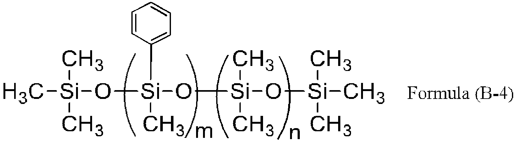
- A mixture composed of 85% by mass of the polyorganosiloxane as the component (A) (the ratio of the component (A) in the component (A) and a component (B-5)) and 15% by mass of a phenyl group-modified silicone as the component (B-5) (trade name TSF433 manufactured by MOMENTIVE INC., weight average molecular weight: 3,000, viscosity: 450 mm2/s) (the ratio of the component (B-5) in the component (A) and the component (B-5)) was mixed with a planetary centrifugal mixer (trade name ARE-500 manufactured by THINKY CORPORATION) for 5 minutes to prepare the (Adhesive 12).

- A mixture composed of 85% by mass of the polyorganosiloxane as the component (A) (the ratio of the component (A) in the component (A) and a component (B-6)) and 15% by mass of a phenyl group-modified silicone as the component (B-6) (trade name PDM-0421 manufactured by Gelest, Inc., weight average molecular weight: 6,200, viscosity: 100 mm2/s) (the ratio of the component (B-6) in the component (A) and the component (B-6)) was mixed with a planetary centrifugal mixer (trade name ARE-500 manufactured by THINKY CORPORATION) for 5 minutes to prepare the (Adhesive 13).

- A mixture composed of 85% by mass of the polyorganosiloxane as the component (A) (the ratio of the component (A) in the component (A) and a component (B-7)) and 15% by mass of a phenyl group-modified silicone as the component (B-7) (trade name PDM-0821 manufactured by Gelest, Inc., weight average molecular weight: 8,600, viscosity: 125 mm2/s) (the ratio of the component (B-7) in the component (A) and the component (B-7)) was mixed with a planetary centrifugal mixer (trade name ARE-500 manufactured by THINKY CORPORATION) for 5 minutes to prepare the (Adhesive 14).

- In order to form a temporary adhesion layer on a 300-mm silicon wafer (thickness: 770 µm) as a wafer on the device side, a film having a thickness of about 50 µm was formed using each of the adhesives (1) to (8) on the circuit side of the wafer by spin coating to form each of adhesion layers (1) to (8), respectively. This wafer having the adhesion layer was attached to a 300-mm glass wafer (thickness: 700 µm) as a wafer (support) on the carrier side with a vacuum attachment device (manual bonder manufactured by SUSS MicroTec AG) so that the adhesion layer was disposed between the wafer and the glass wafer. Thus, a layered body was produced.
- The layered body was then heat-treated at 200°C for 10 minutes on a hot plate. The presence or absence of a void was then checked from the side of the glass wafer (support). Regarding adhesion, a case where no void was observed after the heat treatment is denoted as "○", that is, good, and a case where a void was observed after the heat treatment is denoted as "×", that is, poor. The attached wafer was subsequently heat-treated at 220°C for 10 minutes in an oven under a reduced pressure of 13 Pa. The presence or absence of a void was then checked from the side of the glass wafer (support)-Regarding heat resistance, a case where no void was observed after the heat treatment is denoted as "○", that is, good, and a case where a void was observed after the heat treatment is denoted as "×", that is, poor. Furthermore, in order to check the separation property, the force required for separation was measured with a separation device (manual debonder manufactured by SUSS MicroTec AG). For a case where separation was achieved, the force required for the separation is shown in numerical values as a good result. A case where separation was not achieved is denoted as "×", that is, poor. Moreover, at the time of checking the separation property, the separated interface was checked. A case where the separation occurred at the interface between the wafer on the device side and the adhesion layer, and good control was achieved, is denoted as "Device". A case where the separation occurred at the interface between the wafer (support) on the carrier side and the adhesion layer, and good control was achieved, is denoted as "Carrier". A case where it could not be determined whether the separated interface was on the "Device" side or the "Carrier" side is denoted as "Δ". A case where cohesive failure occurred in the adhesion layer is denoted as "×" A case where separation was not achieved is denoted as "-". The results are shown in Table 1.
Table 1 (Results of Example 1) Adhesion Heat Resistance Separation Property Separated Interface Adhesion Layer (1) ○ ○ × - Adhesion Layer (2) ○ ○ × - Adhesion Layer (3) ○ ○ 26 N Carrier Adhesion Layer (4) ○ ○ 23 N Carrier Adhesion Layer (5) ○ ○ 20 N Carrier Adhesion Layer (6) ○ ○ 19 N Carrier Adhesion Layer (7) ○ ○ 20 N Carrier Adhesion Layer (8) ○ ○ 20 N Carrier - The results shown in Table 1 reveal that the adhesion layers (1) and (2) had good results in terms of adhesion and heat resistance, but did not have a good result in terms of separation property. On the other hand, the adhesion layers (3) to (8) had good results in terms of adhesion, heat resistance, separation property, and control of the separated interface.
- In order to form a temporary adhesion layer on a 300-mm silicon wafer (thickness: 770 µm) as a wafer on the device side, a film having a thickness of about 50 µm was formed using the adhesive (5) on the circuit side of each of three wafers by spin coating to form each of adhesion layers (5-1) to (5-3). This wafer having the adhesion layer was attached to a 300-mm glass wafer (thickness: 700 µm) as a wafer (support) on the carrier side with a vacuum attachment device (manual bonder manufactured by SUSS MicroTec AG) so that the adhesion layer was disposed between the wafer and the glass wafer. Thus, a layered body was produced. The layered body was then heat-treated at 200°C for 10 minutes on a hot plate. At this time, a case where the heat treatment was carried out with the wafer on the device side facing downward is denoted as "Device", and a case where the heat treatment was carried out with the wafer (support) on the carrier side facing downward is denoted as "Carrier". A case where the heat treatment was carried out at 200°C for 10 minutes with an inert gas oven (manufactured by Espec Corporation) is denoted as "Oven".
- Furthermore, in order to check the separation property, the force required for separation was measured with a separation device (manual debonder manufactured by SUSS MicroTec AG). For a case where separation was achieved, the force required for the separation is shown in numerical values as a good result. A case where separation was not achieved is denoted as "×", that is, poor. Moreover, at the time of checking the separation property, the separated interface was checked. A case where the separation occurred at the interface between the wafer on the device side and the adhesion layer, and good control was achieved, is denoted as "Device". A case where the separation occurred at the interface between the wafer (support) on the carrier side and the adhesion layer, and good control was achieved, is denoted as "Carrier". A case where separation was not achieved is denoted as "×", that is, poor. The results are shown in Table 2.
Table 2 (Results of Example 2) Heat-Treated Side Separation Property Separated Interface Adhesion Layer (5-1) Device 20 N Carrier Adhesion Layer (5-2) Carrier 17 N Carrier Adhesion Layer (5-3) Oven 18 N Carrier - The results shown in Table 2 reveal that the adhesion layers (5-1) to (5-3) formed from the adhesive (5) had good results in terms of separation property. The results also confirmed that the separated interface does not change depending on the heat-treatment method carried out in curing the adhesive, and separation can be achieved at the interface between the carrier and the adhesive.
- In order to form a temporary adhesion layer on a 300-mm silicon wafer (thickness: 770 µm) as a wafer on the device side, a film having a thickness of about 100 µm was formed using the adhesive (5) on the circuit side of the wafer by spin coating to form an adhesion layer (5-7). This wafer having the adhesion layer was attached to a 300-mm glass wafer (thickness: 700 µm) as a wafer (support) on the carrier side with a vacuum attachment device (manual bonder manufactured by SUSS MicroTec AG) so that the adhesion layer was disposed between the wafer and the glass wafer. Thus, a layered body was produced. The layered body was then heat-treated at 200°C for 10 minutes on a hot plate with the wafer on the device side facing downward.
- Then, in order to check the separation property, the force required for separation was measured with a separation device (manual debonder manufactured by SUSS MicroTec AG). For a case where separation was achieved, the force required for the separation is shown in numerical values as a good result. A case where separation was not achieved is denoted as "×", that is, poor. Moreover, at the time of checking the separation property, the separated interface was checked. A case where the separation occurred at the interface between the wafer on the device side and the adhesion layer, and good control was achieved, is denoted as "Device". A case where the separation occurred at the interface between the wafer (support) on the carrier side and the adhesion layer, and good control was achieved, is denoted as "Carrier". A case where separation was not achieved is denoted as "×", that is, poor. The results are shown in Table 3.
Table 3 (Results of Example 3) Thickness of Temporary Adhesion Layer Separation Property Separated Interface Adhesion Layer (5-1) 50 µm 20 N Carrier Adhesion Layer (5-7) 100 µm 23 N Carrier - The results shown in Table 3 reveal that the adhesion layer (5-7) formed from the adhesive (5) had a good separation property regardless of the thickness of the adhesion layer.
- In order to form a temporary adhesion layer on a 300-mm silicon wafer (thickness: 770 µm) as a wafer on the device side, a film having a thickness of about 50 µm was formed using the adhesive (5) on the circuit side of each of four wafers by spin coating to form each of adhesion layers (5-8) to (5-11). This wafer having the adhesion layer was attached to a 300-mm glass wafer (thickness: 700 µm) as a wafer (support) on the carrier side with a vacuum attachment device (manual bonder manufactured by SUSS MicroTec AG) so that the adhesion layer was disposed between the wafer and the glass wafer. Thus, a layered body was produced. Each of the layered bodies was then heat-treated at 120, 150, 220, or 260°C for 10 minutes on a hot plate with the wafer on the device side facing downward.
- Then, in order to check the separation property, the force required for separation was measured with a separation device (manual debonder manufactured by SUSS MicroTec AG). For a case where separation was achieved, the force required for the separation is shown in numerical values as a good result. A case where separation was not achieved is denoted as "×", that is, poor. Moreover, at the time of checking the separation property, the separated interface was checked. A case where the separation occurred at the interface between the wafer on the device side and the adhesion layer, and good control was achieved, is denoted as "Device". A case where the separation occurred at the interface between the wafer (support) on the carrier side and the adhesion layer, and good control was achieved, is denoted as "Carrier". A case where separation was not achieved is denoted as "×", that is, poor. The results are shown in Table 4.
Table 4 (Results of Example 4) Heat- Treatment Temperature Separation Property Separated Interface Adhesion Layer (5-8) 120°C 17 N Carrier Adhesion Layer (5-9) 150°C 17 N Carrier Adhesion Layer (5-10) 220°C 18 N Carrier er Adhesion Layer (5-11) 260°C 21 N Carrier er - The results shown in Table 4 reveal that the adhesion layers (5-8) to (5-11) formed from the adhesive (5) had good separation properties regardless of the heat-treatment temperature.
- In order to form a temporary adhesion layer on a 300-mm silicon wafer (thickness: 770 µm) as a wafer on the device side, a film having a thickness of about 50 µm was formed using each of the adhesives (5) and (9) to (14) on the circuit side of the wafer by spin coating to form each of adhesion layers (5-12) and (9) to (14), respectively. This wafer having the adhesion layer was attached to a 300-mm glass wafer (thickness: 700 µm) as a wafer (support) on the carrier side with a vacuum attachment device (manual bonder manufactured by SUSS MicroTec AG) so that the adhesion layer was disposed between the wafer and the glass wafer Thus, a layered body was produced.
- The layered body was then heat-treated at 200°C for 10 minutes on a hot plate with the wafer on the device side facing downward. The presence or absence of a void was then checked from the side of the glass wafer. Regarding adhesion, a case where no void was observed after the heat treatment is denoted as "○", that is, good, and a case where a void was observed after the heat treatment is denoted as "×", that is, poor. Furthermore, in order to check the separation property, the force required for separation was measured with a separation device (manual debonder manufactured by SUSS MicroTec AG). For a case where separation was achieved, the force required for the separation is shown in numerical values as a good result. A case where separation was not achieved is denoted as "×", that is, poor. Moreover, at the time of checking the separation property, the separated interface was checked. A case where the separation occurred at the interface between the wafer on the device side and the adhesion layer, and good control was achieved, is denoted as "Device". A case where the separation occurred at the interface between the wafer (support) on the carrier side and the adhesion layer, and good control was achieved, is denoted as "Carrier". A case where it could not be determined whether the separated interface was on the "Device" side or the "Carrier" side is denoted as "Δ". A case where cohesive failure occurred in the adhesion layer is denoted as "×". A case where separation was not achieved is denoted as "-". The results are shown in Table 5.
Table 5 (Results of Example 5) Adhesion Heat Resistance Separation Property Separated Interface Adhesion Layer (5-12) ○ ○ 20 N Carrier Adhesion Layer (9) ○ ○ 32 N Carrier Adhesion Layer (10) ○ ○ 30 N Carrier Adhesion Layer (11) ○ ○ × - Adhesion Layer (12) ○ ○ × - Adhesion Layer (13) ○ ○ × - Adhesion Layer (14) ○ ○ × - - The results shown in Table 5 reveal that the adhesion layers (5-12), (9), and (10) formed from the adhesive (5) had good adhesion and good separation properties.
- In order to form a temporary adhesion layer on a 300-mm trimmed silicon wafer (thickness: 770 µm) as a wafer on the device side, a film having a thickness of about 50 µm was formed using the adhesive (5) on the circuit side of the wafer by spin coating to form an adhesion layer (5-13). This wafer having the adhesion layer was attached to a 300-mm silicon wafer (thickness: 770 µm) as a wafer (support) on the carrier side with a vacuum attachment device (manual bonder manufactured by SUSS MicroTec AG) so that the adhesion layer was disposed between the wafers. Thus, a layered body was produced.
- The layered body was then heat-treated at 200°C for 10 minutes on a hot plate with the wafer on the device side facing downward. The wafer on the device side was then thinned with a rear surface-grinding device (back grinder manufactured by TOKYO SEIMITSU CO., LTD.). After the thinning, the edge of the wafer on the device side was observed with an optical microscope. A case where chipping did not occur is denoted as "○", that is, good, and a case where chipping occurred is denoted as "×". The result is shown in Table 6.
Table 6 (Result of Example 6) Chipping Adhesion Layer (5-13) ○ - The result shown in Table 6 reveals that in the adhesion layer (5-13) formed from the adhesive (5), chipping was not observed in the thinning process of the wafer on the device side, and a good result was obtained.
- In order to form a temporary adhesion layer on a 300-mm PI wafer (thickness: 770 µm, base: SiN + PI, scribe line: width 100 mm, 15-mm pitch) manufactured by Global Net Corporation as a wafer on the device side, a film having a thickness of about 50 µm was formed using the adhesive (5) on the circuit side of the wafer by spin coating to form an adhesion layer (5-14). This wafer having the adhesion layer was attached to a 300-mm glass wafer (thickness: 770 µm) as a wafer (support) on the carrier side with a vacuum attachment device (manual bonder manufactured by SUSS MicroTec AG) so that the adhesion layer was disposed between the wafer and the glass wafer. Thus, a layered body was produced.
- The layered body was then heat-treated at 200°C for 10 minutes on a hot plate with the wafer on the device side facing downward. Furthermore, in order to check the separation property, separation was carried out between the wafer on the device side and the adhesion layer (5-14) with a separation device (manual debonder manufactured by SUSS MicroTec AG). At this time, although most of the adhesion layer remained on the carrier side, in order to remove a very small amount of the adhesive remaining on the wafer on the device side, paddle cleaning was carried out for 10 minutes with a cleaner composed of tetrabutylammonium fluoride, diazabicycloundecene (DBU), and 2-heptanone. The surface was then observed with an optical microscope. A case where the adhesive was completely removed was evaluated as good, and is denoted as "○", and a case where the adhesive was not completely removed is denoted as "×". The result is shown in Table 7.
Table 7 (Result of Example 7) Cleaning Test Adhesion Layer (5-14) ○ - The result shown in Table 7 reveals that in the adhesion layer (5-14) formed from the adhesive (5), the surface of the wafer on the device side was completely cleaned by paddle cleaning with the aforementioned cleaner, and a good result was obtained.
- In order to form a temporary adhesion layer on a 300-mm PI wafer (thickness: 770 µm, base: SiN + PI, scribe line: width 100 mm, 15-mm pitch) manufactured by Global Net Corporation as a wafer on the device side, a film having a thickness of about 50 µm was formed using the adhesive (5) on the circuit side of the wafer by spin coating to form an adhesion layer (5-15). This wafer having the adhesion layer was attached to a 300-mm glass water (thickness: 770 µm) as a wafer (support) on the carrier side with a vacuum attachment device (manual bonder manufactured by SUSS MicroTec AG) so that the adhesion layer was disposed between the wafer and the glass wafer. Thus, a layered body was produced.
- The layered body was then heat-treated at 200°C for 10 minutes on a hot plate with the wafer on the device side facing downward Furthermore, in order to check the separation property, separation was carried out at the interface between the wafer on the device side and the adhesion layer (5-15) with a separation device (manual debonder manufactured by SUSS MicroTec AG).
- As a comparison, an adhesive composed of the component (A) only was applied at a thickness of about 50 µm to a 300-mm glass wafer (thickness: 770 µm) as a wafer (support) on the carrier side to form an adhesion layer (A-1). The adhesion layer (A-1) was then heat-treated at 200°C for 10 minutes.
- Then, an adhesive separation test was carried out on each of the adhesion layers (5-15) and (A-1) remaining on the wafer (support) on the carrier side, by a tape peeling method using a terminal area-masking tape for printed circuit board plating (trade name N-300 manufactured by Nitto Denko Corporation). The test was carried out by applying the tape to the adhesive surface of the wafer (support) on the carrier side, and peeling off the tape at an angle in the range from 60 to 180° with respect to the wafer (support) on the carrier side, thereby separating each of the adhesion layers (5-15) and (A-1) from the wafer (support) on the carrier side.
- A case where separation was achieved was evaluated as good, and is denoted as "○", and a case where separation was not achieved is denoted as "×".
Table 8 (Results of Example 8) Tape Peeling Test Adhesion Layer (5-15) ○ Adhesion Layer (A-1) × - The results shown in Table 8 reveal that the adhesion layer (5-15) formed from the adhesive (5) was removed by the lift-off process using the aforementioned tape, and a good result was obtained. On the other hand, the results did not confirm the removal by the lift-off process of the adhesion layer (A-1) formed from the component (A) mentioned as a comparative example.
- In order to form a temporary adhesion layer on a 300-mm PI wafer (thickness: 770 µm, base: SiN + PI, scribe line: width 100 mm, 15-mm pitch) manufactured by Global Net Corporation as a wafer on the device side, a film having a thickness of about 50 µm was formed using the adhesive (5) on the circuit side of the wafer by spin coating to form an adhesion layer (5-16). This wafer having the adhesion layer was attached to a 300-mm glass water (thickness: 770 µm) as a wafer (support) on the carrier side with a vacuum attachment device (manual bonder manufactured by SUSS MicroTec AG) so that the adhesion layer was disposed between the wafer and the glass wafer. Thus, a layered body was produced.
- The layered body was then heat-treated at 200°C for 10 minutes on a hot plate with the wafer on the device side facing downward. Furthermore, in order to check the separation property, separation was carried out at the interface between the wafer on the device side and the adhesion layer (5-16) with a separation device (manual debonder manufactured by SUSS MicroTec AG).
- As a comparison, an adhesive composed of the component (A) only was applied at a thickness of about 50 µm to a 300-mm glass wafer (thickness: 770 µm) as a wafer (support) on the carrier side to form an adhesion layer (A-2). The adhesion layer (A-2) was then heat-treated at 200°C for 10 minutes.
- Then, the adhesion layers (5-16) and (A-2) remaining on the wafer (support) on the carrier side were immersed in Isoper-E (hydrocarbon-based solvent manufactured by Andoh Parachemie Co., Ltd.) and Shellsol MC421 (hydrocarbon-based solvent manufactured by Shell Chemicals Japan Ltd.) to remove the adhesion layers using the solvent. A case where the adhesion layer could be removed by lift-off after immersion in the solvent was evaluated as good, and is denoted as "○", and a case where the adhesion layer could not be removed by lift-off after immersion in the solvent is denoted as "×".
Table 9 Results of Example 9) Isoper-E Shellsol MC421 Adhesion Layer (5-16) ○ ○ Adhesion Layer (A-2) × × - A layered body according to the present invention has a temporary adhesion layer as an additive between a support (supporting substrate) and a wafer. An adhesive that forms the temporary adhesion layer contains an adhesive containing a polyorganosiloxane component that is cured by a hydrosilylation reaction and a phenyl group-containing polyorganosiloxane component as an additive. This eliminates the need for forming a separation layer, and makes it possible to achieve easy separation after polishing the rear surface of the wafer.
Claims (14)
- An adhesive for separatably attaching a support to a circuit side of a wafer to process a rear surface of the wafer, the adhesive comprising a component (A) that is cured by a hydrosilylation reaction and a component (B) containing a phenyl group-containing polyorganosiloxane, wherein a ratio in % by mass of the component (A) to the component (B) is 95:5 to 30:70.
- The adhesive according to claim 1, wherein the component (A) comprises:a polysiloxane (Al) comprising a polysiloxane selected from the group consisting of a siloxane unit (Q unit) of SiO2, a siloxane unit (M unit) of R1R2R3SiO1/2, a siloxane unit (D unit) of R4R5SiO2/2, and a siloxane unit (T unit) of R6SiO3/2 (with the proviso that R1 to R6 are each bonded to a silicon atom through a Si-C bond or a Si-H bond), and comprising a polyorganosiloxane (al) wherein monovalent chemical groups of R1 to R6 each contain a C1-10 alkyl group and a C2-10 alkenyl group and a polyorganosiloxane (a2) wherein monovalent chemical groups of R1 to R6 each contain a C1-10 alkyl group and a hydrogen atom; anda platinum group metal-based catalyst (A2).
- The adhesive according to claim 1 or 2, wherein the component (B) is a combination of (b1) a phenylmethylsiloxane unit structure or a diphenylsiloxane unit structure and (b2) a dimethylsiloxane unit structure.
- The adhesive according to any one of claims 1 to 3, wherein the processing is polishing the rear surface of the wafer.
- A method for attaching a layered body comprising applying the adhesive according to any one of claims 1 to 4 onto a first body to form an adhesion layer, attaching a second body to the adhesion layer, and heating the adhesion layer from a side of the first body.
- The method for attaching a layered body according to claim 5, wherein the first body is a support, the second body is a wafer, and a circuit side of the wafer faces the first body.
- The method for attaching a layered body according to claim 5, wherein the first body is a wafer, the second body is a support, and a circuit side of the wafer faces the second body.
- A separation method comprising applying the adhesive according to any one of claims 1 to 3 onto a first body to form an adhesion layer, attaching a second body to the adhesion layer, heating the adhesion layer from a side of the first body to cure the adhesive to form a layered body, processing the layered body, and carrying out separation between the adhesion layer, and the first body and the second body.
- A separation method comprising applying the adhesive according to claim 4 onto a first body to form an adhesion layer, attaching a second body to the adhesion layer, heating the adhesion layer from a side of the first body to cure the adhesive to form a layered body, processing the layered body, and carrying out separation between the adhesion layer, and the first body and the second body.
- The separation method according to claim 8, wherein the first body is a support, the second body is a wafer, and a circuit side of the wafer faces the first body.
- The separation method according to claim 9, wherein the first body is a support, the second body is a wafer, and a circuit side of the wafer faces the first body.
- The separation method according to claim 8, wherein the first body is a wafer, the second body is a support, and a circuit side of the wafer faces the second body.
- The separation method according to claim 9, wherein the first body is a wafer, the second body is a support, and a circuit side of the wafer faces the second body.
- The separation method according to any one of claims 8, 10 and 12, wherein the processing is polishing the rear surface of the wafer.
Applications Claiming Priority (2)
| Application Number | Priority Date | Filing Date | Title |
|---|---|---|---|
| JP2017133094 | 2017-07-06 | ||
| PCT/JP2018/025542 WO2019009365A1 (en) | 2017-07-06 | 2018-07-05 | Temporary adhesive agent containing phenyl-group-containing polysiloxane |
Publications (3)
| Publication Number | Publication Date |
|---|---|
| EP3651186A1 true EP3651186A1 (en) | 2020-05-13 |
| EP3651186A4 EP3651186A4 (en) | 2021-03-17 |
| EP3651186B1 EP3651186B1 (en) | 2025-11-05 |
Family
ID=64950129
Family Applications (1)
| Application Number | Title | Priority Date | Filing Date |
|---|---|---|---|
| EP18828060.6A Active EP3651186B1 (en) | 2017-07-06 | 2018-07-05 | Temporary adhesive agent containing phenyl-group-containing polysiloxane |
Country Status (8)
| Country | Link |
|---|---|
| US (1) | US11345837B2 (en) |
| EP (1) | EP3651186B1 (en) |
| JP (1) | JP7168916B2 (en) |
| KR (1) | KR102520889B1 (en) |
| CN (1) | CN110870049B (en) |
| SG (1) | SG11202000059QA (en) |
| TW (1) | TWI778093B (en) |
| WO (1) | WO2019009365A1 (en) |
Cited By (2)
| Publication number | Priority date | Publication date | Assignee | Title |
|---|---|---|---|---|
| EP3882326A4 (en) * | 2018-11-16 | 2022-08-10 | Nissan Chemical Corporation | ADHESIVE COMPOSITION FOR INFRARED DETACHMENT, LAMINATE, LAMINATE PRODUCTION METHOD AND DETACHMENT METHOD |
| WO2024064735A1 (en) * | 2022-09-20 | 2024-03-28 | Dow Silicones Corporation | Silicone coating composition |
Families Citing this family (3)
| Publication number | Priority date | Publication date | Assignee | Title |
|---|---|---|---|---|
| JP7682807B2 (en) * | 2019-12-02 | 2025-05-26 | 信越化学工業株式会社 | Temporary adhesive for wafer processing, wafer laminate, and method for manufacturing thin wafer |
| EP4083159A4 (en) * | 2019-12-23 | 2024-01-10 | Nissan Chemical Corporation | ADHESIVE COMPOSITION, LAMINATE AND METHOD FOR PRODUCING THE SAME, METHOD FOR PEELING LAMINATE AND METHOD FOR PROCESSING A SEMICONDUCTOR SHAPING SUBSTRATE |
| CN122207393A (en) * | 2023-11-02 | 2026-06-12 | 日产化学株式会社 | Adhesive composition, laminate, and method for producing processed semiconductor substrate |
Family Cites Families (20)
| Publication number | Priority date | Publication date | Assignee | Title |
|---|---|---|---|---|
| JP3998438B2 (en) | 2001-06-22 | 2007-10-24 | 信越化学工業株式会社 | Adhesive for polymer electrolyte fuel cells |
| US7482249B2 (en) | 2002-11-29 | 2009-01-27 | Fraunhofer-Gesellschaft Zur Forderung Der Angewandten Forschung E.V. | Method and device for machining a wafer, in addition to a wafer comprising a separation layer and a support layer |
| EP1854136A1 (en) | 2005-03-01 | 2007-11-14 | Dow Corning Corporation | Temporary wafer bonding method for semiconductor processing |
| WO2007099146A1 (en) | 2006-03-01 | 2007-09-07 | Jakob + Richter Ip-Verwertungsgesellschaft Mbh | Method for processing, in particular, thin rear sides of a wafer, wafer-carrier arrangement and method for producing said type of wafer-carrier arrangement |
| JP2010070599A (en) * | 2008-09-17 | 2010-04-02 | Dow Corning Toray Co Ltd | Liquid die bonding agent |
| DE102008044200B4 (en) | 2008-11-28 | 2012-08-23 | Thin Materials Ag | Bonding method |
| DE102008055155B4 (en) | 2008-12-23 | 2026-07-30 | Nissan Chemical Industries, Ltd. | Separation method for a layer system comprising a wafer, use of a polymethacrylate disc in the method and apparatus for carrying out the method |
| US8647964B2 (en) | 2010-02-12 | 2014-02-11 | Dow Corning Corporation | Temporary wafer bonding method for semiconductor processing |
| JP5348147B2 (en) * | 2011-01-11 | 2013-11-20 | 信越化学工業株式会社 | Temporary adhesive composition and method for producing thin wafer |
| JP5409695B2 (en) * | 2011-04-26 | 2014-02-05 | 信越化学工業株式会社 | Organopolysiloxane, temporary adhesive composition containing organopolysiloxane, and thin wafer manufacturing method using the same |
| DE102011079687A1 (en) * | 2011-07-22 | 2013-01-24 | Wacker Chemie Ag | Temporary bonding of chemically similar substrates |
| JP5687230B2 (en) | 2012-02-28 | 2015-03-18 | 信越化学工業株式会社 | Wafer processing body, wafer processing member, wafer processing temporary adhesive, and thin wafer manufacturing method |
| JP5767159B2 (en) | 2012-04-27 | 2015-08-19 | 信越化学工業株式会社 | Wafer processing body, wafer processing member, wafer processing temporary adhesive, and thin wafer manufacturing method |
| CN105452386B (en) * | 2013-08-09 | 2018-12-11 | 横滨橡胶株式会社 | Curable resin composition |
| CN105814142A (en) | 2013-12-16 | 2016-07-27 | 迈图高新材料日本合同公司 | Addition-curable silicone composition |
| CN106715591A (en) * | 2014-06-03 | 2017-05-24 | 道康宁东丽株式会社 | Curable silicone composition and optical semiconductor device |
| JP6583639B2 (en) * | 2014-06-10 | 2019-10-02 | 日産化学株式会社 | Laminated body using temporary adhesive |
| JP6325432B2 (en) * | 2014-12-25 | 2018-05-16 | 信越化学工業株式会社 | Wafer processed body, temporary adhesive for wafer processing, and method for manufacturing thin wafer |
| US20180037013A1 (en) * | 2015-03-05 | 2018-02-08 | Dow Corning Toray Co., Ltd. | Curable organopolysiloxane composition, a use thereof, and a laminate prepared from the composition |
| TWI837219B (en) * | 2018-11-16 | 2024-04-01 | 日商日產化學股份有限公司 | Adhesive composition for infrared peeling, laminate, manufacturing method of laminate, and peeling method |
-
2018
- 2018-07-05 KR KR1020207001260A patent/KR102520889B1/en active Active
- 2018-07-05 SG SG11202000059QA patent/SG11202000059QA/en unknown
- 2018-07-05 CN CN201880045131.8A patent/CN110870049B/en active Active
- 2018-07-05 US US16/627,993 patent/US11345837B2/en active Active
- 2018-07-05 EP EP18828060.6A patent/EP3651186B1/en active Active
- 2018-07-05 JP JP2019527965A patent/JP7168916B2/en active Active
- 2018-07-05 WO PCT/JP2018/025542 patent/WO2019009365A1/en not_active Ceased
- 2018-07-06 TW TW107123429A patent/TWI778093B/en active
Cited By (2)
| Publication number | Priority date | Publication date | Assignee | Title |
|---|---|---|---|---|
| EP3882326A4 (en) * | 2018-11-16 | 2022-08-10 | Nissan Chemical Corporation | ADHESIVE COMPOSITION FOR INFRARED DETACHMENT, LAMINATE, LAMINATE PRODUCTION METHOD AND DETACHMENT METHOD |
| WO2024064735A1 (en) * | 2022-09-20 | 2024-03-28 | Dow Silicones Corporation | Silicone coating composition |
Also Published As
| Publication number | Publication date |
|---|---|
| EP3651186A4 (en) | 2021-03-17 |
| KR102520889B1 (en) | 2023-04-12 |
| US11345837B2 (en) | 2022-05-31 |
| TW201920582A (en) | 2019-06-01 |
| JP7168916B2 (en) | 2022-11-10 |
| US20200216731A1 (en) | 2020-07-09 |
| KR20200026895A (en) | 2020-03-11 |
| TWI778093B (en) | 2022-09-21 |
| WO2019009365A1 (en) | 2019-01-10 |
| JPWO2019009365A1 (en) | 2020-04-30 |
| CN110870049A (en) | 2020-03-06 |
| EP3651186B1 (en) | 2025-11-05 |
| SG11202000059QA (en) | 2020-02-27 |
| CN110870049B (en) | 2023-10-03 |
Similar Documents
| Publication | Publication Date | Title |
|---|---|---|
| US12617988B2 (en) | Temporary adhesive containing epoxy-modified polysiloxane | |
| JP6916470B2 (en) | Adhesive containing polydimethylsiloxane | |
| JP6583639B2 (en) | Laminated body using temporary adhesive | |
| EP3651186B1 (en) | Temporary adhesive agent containing phenyl-group-containing polysiloxane | |
| US12559655B2 (en) | Polysiloxane-containing temporary adhesive comprising heat-resistant polymerization inhibitor | |
| US20250215294A1 (en) | Adhesive containing polyether-modified siloxane |
Legal Events
| Date | Code | Title | Description |
|---|---|---|---|
| STAA | Information on the status of an ep patent application or granted ep patent |
Free format text: STATUS: THE INTERNATIONAL PUBLICATION HAS BEEN MADE |
|
| PUAI | Public reference made under article 153(3) epc to a published international application that has entered the european phase |
Free format text: ORIGINAL CODE: 0009012 |
|
| STAA | Information on the status of an ep patent application or granted ep patent |
Free format text: STATUS: REQUEST FOR EXAMINATION WAS MADE |
|
| 17P | Request for examination filed |
Effective date: 20200113 |
|
| AK | Designated contracting states |
Kind code of ref document: A1 Designated state(s): AL AT BE BG CH CY CZ DE DK EE ES FI FR GB GR HR HU IE IS IT LI LT LU LV MC MK MT NL NO PL PT RO RS SE SI SK SM TR |
|
| AX | Request for extension of the european patent |
Extension state: BA ME |
|
| DAV | Request for validation of the european patent (deleted) | ||
| DAX | Request for extension of the european patent (deleted) | ||
| REG | Reference to a national code |
Ref country code: DE Ref legal event code: R079 Ipc: C09J0005060000 Ref country code: DE Ref legal event code: R079 Ref document number: 602018086965 Country of ref document: DE Free format text: PREVIOUS MAIN CLASS: H01L0021304000 Ipc: C09J0005060000 |
|
| A4 | Supplementary search report drawn up and despatched |
Effective date: 20210211 |
|
| RIC1 | Information provided on ipc code assigned before grant |
Ipc: H01L 21/304 20060101ALI20210205BHEP Ipc: C09J 183/04 20060101ALI20210205BHEP Ipc: H01L 21/683 20060101ALI20210205BHEP Ipc: H01L 21/02 20060101ALI20210205BHEP Ipc: C09J 201/02 20060101ALI20210205BHEP Ipc: C09J 183/07 20060101ALI20210205BHEP Ipc: C09J 5/06 20060101AFI20210205BHEP |
|
| STAA | Information on the status of an ep patent application or granted ep patent |
Free format text: STATUS: EXAMINATION IS IN PROGRESS |
|
| 17Q | First examination report despatched |
Effective date: 20240402 |
|
| GRAP | Despatch of communication of intention to grant a patent |
Free format text: ORIGINAL CODE: EPIDOSNIGR1 |
|
| STAA | Information on the status of an ep patent application or granted ep patent |
Free format text: STATUS: GRANT OF PATENT IS INTENDED |
|
| RIC1 | Information provided on ipc code assigned before grant |
Ipc: C09J 5/06 20060101AFI20250610BHEP Ipc: C09J 183/04 20060101ALI20250610BHEP Ipc: H01L 21/683 20060101ALI20250610BHEP |
|
| INTG | Intention to grant announced |
Effective date: 20250703 |
|
| GRAS | Grant fee paid |
Free format text: ORIGINAL CODE: EPIDOSNIGR3 |
|
| GRAA | (expected) grant |
Free format text: ORIGINAL CODE: 0009210 |
|
| STAA | Information on the status of an ep patent application or granted ep patent |
Free format text: STATUS: THE PATENT HAS BEEN GRANTED |
|
| P01 | Opt-out of the competence of the unified patent court (upc) registered |
Free format text: CASE NUMBER: UPC_APP_7029_3651186/2025 Effective date: 20250912 |
|
| AK | Designated contracting states |
Kind code of ref document: B1 Designated state(s): AL AT BE BG CH CY CZ DE DK EE ES FI FR GB GR HR HU IE IS IT LI LT LU LV MC MK MT NL NO PL PT RO RS SE SI SK SM TR |
|
| REG | Reference to a national code |
Ref country code: CH Ref legal event code: F10 Free format text: ST27 STATUS EVENT CODE: U-0-0-F10-F00 (AS PROVIDED BY THE NATIONAL OFFICE) Effective date: 20251105 Ref country code: GB Ref legal event code: FG4D |
|
| REG | Reference to a national code |
Ref country code: DE Ref legal event code: R096 Ref document number: 602018086965 Country of ref document: DE |
|
| REG | Reference to a national code |
Ref country code: IE Ref legal event code: FG4D |
|
| REG | Reference to a national code |
Ref country code: NL Ref legal event code: MP Effective date: 20251105 |
|
| PG25 | Lapsed in a contracting state [announced via postgrant information from national office to epo] |
Ref country code: ES Free format text: LAPSE BECAUSE OF FAILURE TO SUBMIT A TRANSLATION OF THE DESCRIPTION OR TO PAY THE FEE WITHIN THE PRESCRIBED TIME-LIMIT Effective date: 20251105 |
|
| REG | Reference to a national code |
Ref country code: LT Ref legal event code: MG9D |
|
| PG25 | Lapsed in a contracting state [announced via postgrant information from national office to epo] |
Ref country code: NO Free format text: LAPSE BECAUSE OF FAILURE TO SUBMIT A TRANSLATION OF THE DESCRIPTION OR TO PAY THE FEE WITHIN THE PRESCRIBED TIME-LIMIT Effective date: 20260205 |
|
| PG25 | Lapsed in a contracting state [announced via postgrant information from national office to epo] |
Ref country code: HR Free format text: LAPSE BECAUSE OF FAILURE TO SUBMIT A TRANSLATION OF THE DESCRIPTION OR TO PAY THE FEE WITHIN THE PRESCRIBED TIME-LIMIT Effective date: 20251105 Ref country code: FI Free format text: LAPSE BECAUSE OF FAILURE TO SUBMIT A TRANSLATION OF THE DESCRIPTION OR TO PAY THE FEE WITHIN THE PRESCRIBED TIME-LIMIT Effective date: 20251105 Ref country code: AT Free format text: LAPSE BECAUSE OF FAILURE TO SUBMIT A TRANSLATION OF THE DESCRIPTION OR TO PAY THE FEE WITHIN THE PRESCRIBED TIME-LIMIT Effective date: 20251105 |
|
| REG | Reference to a national code |
Ref country code: AT Ref legal event code: MK05 Ref document number: 1854346 Country of ref document: AT Kind code of ref document: T Effective date: 20251105 |
|
| PG25 | Lapsed in a contracting state [announced via postgrant information from national office to epo] |
Ref country code: NL Free format text: LAPSE BECAUSE OF FAILURE TO SUBMIT A TRANSLATION OF THE DESCRIPTION OR TO PAY THE FEE WITHIN THE PRESCRIBED TIME-LIMIT Effective date: 20251105 |
|
| PG25 | Lapsed in a contracting state [announced via postgrant information from national office to epo] |
Ref country code: RS Free format text: LAPSE BECAUSE OF FAILURE TO SUBMIT A TRANSLATION OF THE DESCRIPTION OR TO PAY THE FEE WITHIN THE PRESCRIBED TIME-LIMIT Effective date: 20260205 |
|
| PG25 | Lapsed in a contracting state [announced via postgrant information from national office to epo] |
Ref country code: IS Free format text: LAPSE BECAUSE OF FAILURE TO SUBMIT A TRANSLATION OF THE DESCRIPTION OR TO PAY THE FEE WITHIN THE PRESCRIBED TIME-LIMIT Effective date: 20260305 |
|
| PG25 | Lapsed in a contracting state [announced via postgrant information from national office to epo] |
Ref country code: PT Free format text: LAPSE BECAUSE OF FAILURE TO SUBMIT A TRANSLATION OF THE DESCRIPTION OR TO PAY THE FEE WITHIN THE PRESCRIBED TIME-LIMIT Effective date: 20260305 |
|
| PG25 | Lapsed in a contracting state [announced via postgrant information from national office to epo] |
Ref country code: PL Free format text: LAPSE BECAUSE OF FAILURE TO SUBMIT A TRANSLATION OF THE DESCRIPTION OR TO PAY THE FEE WITHIN THE PRESCRIBED TIME-LIMIT Effective date: 20251105 |
|
| PG25 | Lapsed in a contracting state [announced via postgrant information from national office to epo] |
Ref country code: LV Free format text: LAPSE BECAUSE OF FAILURE TO SUBMIT A TRANSLATION OF THE DESCRIPTION OR TO PAY THE FEE WITHIN THE PRESCRIBED TIME-LIMIT Effective date: 20251105 |
|
| PG25 | Lapsed in a contracting state [announced via postgrant information from national office to epo] |
Ref country code: BG Free format text: LAPSE BECAUSE OF FAILURE TO SUBMIT A TRANSLATION OF THE DESCRIPTION OR TO PAY THE FEE WITHIN THE PRESCRIBED TIME-LIMIT Effective date: 20251105 |
|
| PG25 | Lapsed in a contracting state [announced via postgrant information from national office to epo] |
Ref country code: LT Free format text: LAPSE BECAUSE OF FAILURE TO SUBMIT A TRANSLATION OF THE DESCRIPTION OR TO PAY THE FEE WITHIN THE PRESCRIBED TIME-LIMIT Effective date: 20251105 |
|
| PG25 | Lapsed in a contracting state [announced via postgrant information from national office to epo] |
Ref country code: SM Free format text: LAPSE BECAUSE OF FAILURE TO SUBMIT A TRANSLATION OF THE DESCRIPTION OR TO PAY THE FEE WITHIN THE PRESCRIBED TIME-LIMIT Effective date: 20251105 |
|
| PG25 | Lapsed in a contracting state [announced via postgrant information from national office to epo] |
Ref country code: DK Free format text: LAPSE BECAUSE OF FAILURE TO SUBMIT A TRANSLATION OF THE DESCRIPTION OR TO PAY THE FEE WITHIN THE PRESCRIBED TIME-LIMIT Effective date: 20251105 |
|
| PG25 | Lapsed in a contracting state [announced via postgrant information from national office to epo] |
Ref country code: IT Free format text: LAPSE BECAUSE OF FAILURE TO SUBMIT A TRANSLATION OF THE DESCRIPTION OR TO PAY THE FEE WITHIN THE PRESCRIBED TIME-LIMIT Effective date: 20251105 |
|
| PG25 | Lapsed in a contracting state [announced via postgrant information from national office to epo] |
Ref country code: EE Free format text: LAPSE BECAUSE OF FAILURE TO SUBMIT A TRANSLATION OF THE DESCRIPTION OR TO PAY THE FEE WITHIN THE PRESCRIBED TIME-LIMIT Effective date: 20251105 |
|
| PG25 | Lapsed in a contracting state [announced via postgrant information from national office to epo] |
Ref country code: CZ Free format text: LAPSE BECAUSE OF FAILURE TO SUBMIT A TRANSLATION OF THE DESCRIPTION OR TO PAY THE FEE WITHIN THE PRESCRIBED TIME-LIMIT Effective date: 20251105 |
|
| PG25 | Lapsed in a contracting state [announced via postgrant information from national office to epo] |
Ref country code: SK Free format text: LAPSE BECAUSE OF FAILURE TO SUBMIT A TRANSLATION OF THE DESCRIPTION OR TO PAY THE FEE WITHIN THE PRESCRIBED TIME-LIMIT Effective date: 20251105 |
|
| PG25 | Lapsed in a contracting state [announced via postgrant information from national office to epo] |
Ref country code: SE Free format text: LAPSE BECAUSE OF FAILURE TO SUBMIT A TRANSLATION OF THE DESCRIPTION OR TO PAY THE FEE WITHIN THE PRESCRIBED TIME-LIMIT Effective date: 20251105 |