EP3648356A1 - Word alignment using deserializer pattern detection - Google Patents
Word alignment using deserializer pattern detection Download PDFInfo
- Publication number
- EP3648356A1 EP3648356A1 EP19199040.7A EP19199040A EP3648356A1 EP 3648356 A1 EP3648356 A1 EP 3648356A1 EP 19199040 A EP19199040 A EP 19199040A EP 3648356 A1 EP3648356 A1 EP 3648356A1
- Authority
- EP
- European Patent Office
- Prior art keywords
- alignment
- circuit
- stage
- flip
- deserializer
- Prior art date
- Legal status (The legal status is an assumption and is not a legal conclusion. Google has not performed a legal analysis and makes no representation as to the accuracy of the status listed.)
- Granted
Links
Images




Classifications
-
- H—ELECTRICITY
- H03—ELECTRONIC CIRCUITRY
- H03M—CODING; DECODING; CODE CONVERSION IN GENERAL
- H03M9/00—Parallel/series conversion or vice versa
-
- H—ELECTRICITY
- H04—ELECTRIC COMMUNICATION TECHNIQUE
- H04J—MULTIPLEX COMMUNICATION
- H04J3/00—Time-division multiplex systems
- H04J3/02—Details
- H04J3/06—Synchronising arrangements
-
- G—PHYSICS
- G06—COMPUTING OR CALCULATING; COUNTING
- G06F—ELECTRIC DIGITAL DATA PROCESSING
- G06F1/00—Details not covered by groups G06F3/00 - G06F13/00 and G06F21/00
- G06F1/04—Generating or distributing clock signals or signals derived directly therefrom
-
- G—PHYSICS
- G06—COMPUTING OR CALCULATING; COUNTING
- G06F—ELECTRIC DIGITAL DATA PROCESSING
- G06F1/00—Details not covered by groups G06F3/00 - G06F13/00 and G06F21/00
- G06F1/24—Resetting means
Definitions
- One or more aspects of embodiments according to the present disclosure relate to serial to parallel conversion, and more particularly to a system and method for word alignment using deserializer pattern detection.
- a deserializer circuit may be used in various applications, e.g., to convert a serial data stream to a parallel data stream.
- a reset signal for the entire system may not be available, and it may be advantageous to infer word boundaries in the received data stream from the data stream itself. Such a process may be referred to as word alignment.
- a system for word alignment including: a deserializer circuit; an alignment detection circuit; and a clock generator circuit, the clock generator circuit having: a plurality of enable outputs connected to a plurality of enable inputs of the deserializer circuit, and a plurality of clock outputs connected to a plurality of clock inputs of the deserializer circuit; the alignment detection circuit being configured: to detect a coarse word alignment; and in response to detecting the coarse word alignment, to cause a reset of the clock generator circuit.
- the deserializer circuit includes a plurality of stages, each stage including: one or more demultiplexers, and a plurality of flip-flops, each having a data input connected to a respective output of one of the one or more demultiplexers.
- a data output of a first flip-flop of a first stage of the plurality of stages is connected to an input of the alignment detection circuit; the alignment detection circuit is configured to detect the coarse word alignment from a change in value at the data output of the first flip-flop; and the first stage is not the last stage of the deserializer circuit.
- the alignment detection circuit is further configured, in response to detecting the coarse word alignment, to capture a fine alignment code.
- system further includes a fine alignment circuit configured to adjust word alignment in increments of one bit position.
- the fine alignment circuit includes: a plurality of shift blocks having delays differing by one bit position; and a demultiplexer configured to select a data stream from one of the shift blocks.
- the alignment detection circuit is further configured, in response to detecting the coarse word alignment, to capture a fine alignment code; and the demultiplexer of the fine alignment circuit is configured to select a data stream from one of the shift blocks based on the fine alignment code.
- the deserializer circuit includes a plurality of stages, each stage including: one or more demultiplexers, and a plurality of flip-flops, each having a data input connected to a respective output of one of the one or more demultiplexers; a data output of a first flip-flop of a first stage of the plurality of stages is connected to an input of the alignment detection circuit; the alignment detection circuit is configured to detect the coarse word alignment from a change in value at the data output of the first flip-flop; and the first stage is not the last stage of the deserializer circuit.
- the alignment detection circuit is further configured, in response to detecting the coarse word alignment, to capture a fine alignment code.
- the fine alignment code includes output signals from all of the flip-flops of the first stage except the first flip-flop.
- a method for word alignment in a system including: a deserializer circuit, and a clock generator circuit, the method including: deserializing a received data stream, by the deserializer circuit; detecting a coarse word alignment in the received data stream; and in response to detecting the coarse word alignment, resetting the clock generator circuit.
- the deserializer circuit includes a plurality of stages, each stage including: one or more demultiplexers, and a plurality of flip-flops, each having a data input connected to a respective output of one of the one or more demultiplexers.
- the detecting of the coarse word alignment includes detecting a change in value at a data output of a first flip-flop of a first stage of the plurality of stages; and the first stage is not the last stage of the deserializer circuit.
- the method further includes, in response to detecting the coarse word alignment, capturing a fine alignment code.
- the method further includes adjusting word alignment by one bit position.
- the system further includes a plurality of shift blocks having delays differing by one bit position.
- the method further includes: in response to detecting the coarse word alignment, capturing a fine alignment code; and selecting a data stream from one of the shift blocks based on the fine alignment code.
- the deserializer circuit includes a plurality of stages, each stage including: one or more demultiplexers, and a plurality of flip-flops, each having a data input connected to a respective output of one of the one or more demultiplexers;
- the detecting of the coarse word alignment includes detecting a change in value at a data output of a first flip-flop of a first stage of the plurality of stages; and the first stage is not the last stage of the deserializer circuit.
- the fine alignment code includes output signals from all of the flip-flops of the first stage except the first flip-flop.
- a system for word alignment including: a deserializer circuit; a clock generator circuit; and means for: detecting a coarse word alignment; and in response to detecting the coarse word alignment, resetting the clock generator circuit.
- a deserializer circuit may include several stages, e.g., a first stage 105, a second stage 110, and a third stage 115. Each of the stages may include one or more demultiplexers 120 and a plurality of flip-flops 125.
- each box labeled "FF" represents an array of flip-flops, the number of flip-flops in each array being equal to the width of the busses at the input and output of the array of flip-flops.
- the first stage 105 has a 1-to-2 demultiplexer connected by a 2-bit wide bus (as indicated by the label "/2") to an array of two flip flops.
- the deserializer circuit has between 2 and 8 stages.
- Each demultiplexer 120 directs the signal at its input to one of its outputs, depending on the value of a control signal (or "enable signal") it receives.
- the flip-flops of the deserializer circuit latch the received signal at an edge of a clock signal; the clock signals of successive stages have decreasing frequencies, corresponding to each stage's producing wider parallel data at a lower update rate than the previous stage.
- the enable signal and the clock signals may be generated by a clock generator circuit described in further detail below.
- the clock generator circuit may generate a combination of enable signals that result in the next serial bit received being directed to a first one of the outputs of the deserializer circuit (e.g., the top-most one of the 12 outputs of the deserializer circuit of FIG. 1 ); after the reset, each subsequent bit of the received serial data stream (or "bit stream") is directed to a different one of the outputs of the deserializer circuit, until each output has received one bit, at which point the next serial bit received is again directed to the first one of the outputs of the deserializer circuit.
- a first one of the outputs of the deserializer circuit e.g., the top-most one of the 12 outputs of the deserializer circuit of FIG. 1
- each subsequent bit of the received serial data stream or "bit stream" is directed to a different one of the outputs of the deserializer circuit, until each output has received one bit, at which point the next serial bit received is again directed to the first one of the outputs of the deserializer circuit.
- the output of the deserializer is a series of output data words (e.g., 12-bit wide data words, in the embodiment of FIG. 1 ), which may correspond to input data words fed into a serializer in a serial transmitter.
- Word alignment may be used to ensure that the output data words are the same as the input data words. If word alignment were not performed, or were performed incorrectly, a situation could arise in which instead each output data word corresponds to two fragments of successive input data words. In some embodiments the word length is between 6 bits and 128 bits.
- Word alignment may be performed by arranging for the transmitter to repeatedly transmit a data word consisting of a set bit pattern (e.g., "000111111000"); the receiver may then infer from the received bit stream where the word boundaries are.
- FIGs. 2A and 2B show how correct placement of the word boundaries in the receiver ( FIG. 2A ) may result in the output data words being the same as the input data words (i.e., the set bit pattern) and how incorrect placement of the word boundaries ( FIG. 2B ) may result in the output data words being different from the input data words.
- the set bit pattern may include a total of L zeros and M ones, with L about equal to M, and with the ones being substantially in the middle of the set bit pattern.
- L or M may be larger or equal to the number of bits in the decimated pattern (e.g., 4 bits, in the examples of FIG. 3 (discussed in further detail below)), and for zeros and ones to be consecutive, without necessarily being in the middle of the pattern. It will be understood that a complementary bit pattern may be used instead, to similar effect.
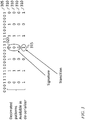
- FIG. 3 shows a received serial bit stream 305 and four decimated patterns 310 that may be produced, for example, by the four outputs of the second stage 110 of the deserializer circuit of FIG. 1 .
- Time progresses from left to right in FIG. 3 .
- an alignment detection circuit detects coarse word alignment by testing for a change in value (e.g., a transition from zero to one) of one of the decimated patterns 310 (e.g., the fourth, or lowest, one of the four rows in FIG. 3 ). Such a change is labeled as a transition 315 in FIG. 3 .
- the fourth decimated pattern has a value of one and its previous value (shown immediately to its left in FIG. 3 ) was zero.
- the system for word alignment performs a reset of the clock generator circuit when coarse word alignment is detected.
- the values of the other three decimated patterns 310 form a "fine alignment code" 320 (or "signature") (e.g., a 3-bit word, in the embodiment of FIG. 3 ) that may be used to perform fine alignment, as discussed in further detail below.
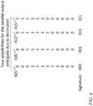
- Coarse word alignment may be detected for any of several possible word alignments of the received bit stream 305, as illustrated in FIG. 4.
- FIG. 4 shows, in a first column, the received serial bit stream 305 for the circumstances of FIG. 3 , and, in the remaining three columns, the received serial bit streams 405, 410, 415 for three other bit alignments of the received serial bit stream, each of which would result in coarse word alignment detection at the same time.
- the fine alignment code differs for the four columns and may therefore be used to determine which of the four possible bit streams 305, 405, 410, 415 was present when coarse word alignment was detected.
- the raw output of the deserializer circuit may correspond to word boundaries that are incorrect by some number of bit positions (e.g., 1, 2, or 3 bit positions in the embodiment of FIG. 3 ).
- a fine alignment circuit may then be used to correct these alignment errors, based on the fine alignment code, as mentioned above and as discussed in further detail below.
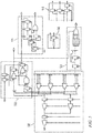
- a circuit for word alignment and deserialization includes a deserializer circuit 505, an alignment detection circuit 510; a clock generator circuit 515, and a fine alignment circuit 520.
- FIG. 5 also shows the internal circuits of the 1-to-2 demultiplexers 540 and of the 1-to-3 demultiplexers 545 (each being an example of a demultiplexer 120 ( FIG. 1 )) of the deserializer circuit 505.
- the deserializer circuit 505 includes three stages, like the deserializer circuit of FIG. 1 , the first stage deserializing the data by a factor of two, the second stage deserializing the data by a further factor of two, and the third stage deserializing the data by a further factor of three.
- the outputs of the second stage are the decimated outputs discussed in the context of FIG. 3 above, and are fed to the alignment detection circuit 510.
- the raw fully deserialized output is fed to the fine alignment circuit 520.
- the alignment detection circuit 510 includes a three-input AND gate 620 with a flip-flop 625 for delaying the signal at one of the inputs, for detecting a zero-to-one transition in one of the decimated outputs (the one fed to the fourth (i.e., lowest) 1-to-3 demultiplexer of the 1-to-3 demultiplexers 545 of the third stage of the deserializer circuit 505).
- Two of the inputs of the three-input AND gate 620 are fed by this decimated output (one of the inputs of the three-input AND gate 620, the inverting input, being fed through the flip-flop 625).
- the remaining input of the three-input AND gate 620 is fed by the output of an output enable flip-flop 630 which is set at startup (under the control of the output enable signal 635 received by the alignment detection circuit 510).
- the three-input AND gate 620 detects coarse word alignment, it resets the output enable flip-flop 630 (preventing further detections of coarse word alignment) and resets the clock generator circuit 515 by asserting the clock generator reset output 640.
- the three-input AND gate 620 detects coarse word alignment, it also causes the data from the three other decimated outputs to be fed, through the fine alignment code output 645, to the fine alignment circuit 520, as the fine alignment code.
- the clock generator circuit 515 includes a first divide-by-two counter 650 for generating a half-rate clock for the first stage of the deserializer circuit 505, a second divide-by-two counter 655 for generating a quarter-rate clock for the second stage of the deserializer circuit 505, and a three-bit ring counter 660 for generating a one-twelfth rate clock for the third stage of the deserializer circuit 505.
- the clock generator circuit 515 may be reset by a signal received (from the alignment detection circuit 510) at the reset input 665 of the clock generator circuit 515.
- the clock generator circuit 515 may include an OR gate configured to cause the duty cycle of the one-twelfth rate clock to be 50%. The use of a clock with a 50% duty cycle may improve timing margin; in some embodiments the duty cycle may be greater or less than 50%.
- the fine alignment circuit 520 includes a first bank of twelve flip-flops 685 and a second bank of twelve flip-flops 690, for storing the two most recently received raw data words from the deserializer circuit 505.
- the fine alignment circuit 520 further includes four shift blocks 675, and a multiplexer 680 for selecting from among the four shift blocks 675 based on the fine alignment code received from the alignment detection circuit 510.
- the first one of the four shift blocks 675 may correspond to a fine alignment code indicating that no fine alignment adjustment is necessary; it may contain wires connecting the outputs of the flip-flops of the first bank of flip-flops 685 to the (12-wide) output of the first one of the four shift blocks 675 (which is connected to a first 12-wide input (of the four such inputs) of the multiplexer 680).
- the second one of the four shift blocks 675 may correspond to a fine alignment error of one bit position; it may contain wires connecting (i) the outputs of eleven of the flip-flops of the first bank of flip-flops 685 and (ii) the output of one of the flip-flops of the second bank of flip-flops 690, to the (12-wide) output of the second one of the four shift blocks 675.
- the "Shift-2" and “Shift-3" shift blocks 675 may similarly each contain wires for feeding, to a respective 12-wide input (of the four such inputs) of the multiplexer 680, a different combination of outputs from the first bank of flip-flops 685 and outputs from the second bank of flip-flops 690.
- the decimation ratio (which is greater than the size of the fine alignment code by one) is four. It will be understood that this ratio may be selected to be greater or smaller, by extracting the decimated outputs after a different stage of the deserializer circuit 505 or by changing the deserialization ratio of one or more of the stages, or both. A smaller value of the decimation ratio may result in a smaller signature size, and, accordingly, a smaller fine alignment circuit 520. However, a smaller value of the decimation ratio may result in the transition detection circuits operating at higher speed, making timing requirements more difficult to meet.
- a circuit for word alignment and deserialization may be a processing circuit, different from that of FIGs. 5 and 6A-6D , configured to perform the methods described herein.
- processing circuit is used herein to mean any combination of hardware, firmware, and software, employed to process data or digital signals.
- Processing circuit hardware may include, for example, application specific integrated circuits (ASICs), general purpose or special purpose central processing units (CPUs), digital signal processors (DSPs), graphics processing units (GPUs), and programmable logic devices such as field programmable gate arrays (FPGAs).
- ASICs application specific integrated circuits
- CPUs general purpose or special purpose central processing units
- DSPs digital signal processors
- GPUs graphics processing units
- FPGAs programmable logic devices
- each function is performed either by hardware configured, i.e., hard-wired, to perform that function, or by more general purpose hardware, such as a CPU, configured to execute instructions stored in a non-transitory storage medium.
- a processing circuit may be fabricated on a single printed circuit board (PCB) or distributed over several interconnected PCBs.
- a processing circuit may contain other processing circuits; for example a processing circuit may include two processing circuits, an FPGA and a CPU, interconnected on a PCB.
- first, second, third, etc. may be used herein to describe various elements, components, regions, layers and/or sections, these elements, components, regions, layers and/or sections should not be limited by these terms. These terms are only used to distinguish one element, component, region, layer or section from another element, component, region, layer or section. Thus, a first element, component, region, layer or section discussed herein could be termed a second element, component, region, layer or section, without departing from the scope of the claims.
- any numerical range recited herein is intended to include all sub-ranges of the same numerical precision subsumed within the recited range.
- a range of "1.0 to 10.0" or “between 1.0 and 10.0” is intended to include all subranges between (and including) the recited minimum value of 1.0 and the recited maximum value of 10.0, that is, having a minimum value equal to or greater than 1.0 and a maximum value equal to or less than 10.0, such as, for example, 2.4 to 7.6.
- Any maximum numerical limitation recited herein is intended to include all lower numerical limitations subsumed therein and any minimum numerical limitation recited in this specification is intended to include all higher numerical limitations subsumed therein.
Landscapes
- Engineering & Computer Science (AREA)
- Theoretical Computer Science (AREA)
- General Engineering & Computer Science (AREA)
- General Physics & Mathematics (AREA)
- Physics & Mathematics (AREA)
- Signal Processing (AREA)
- Computer Networks & Wireless Communication (AREA)
- Design And Manufacture Of Integrated Circuits (AREA)
- Synchronisation In Digital Transmission Systems (AREA)
- Health & Medical Sciences (AREA)
- Artificial Intelligence (AREA)
- Audiology, Speech & Language Pathology (AREA)
- Computational Linguistics (AREA)
- General Health & Medical Sciences (AREA)
- Information Transfer Systems (AREA)
Abstract
Description
- One or more aspects of embodiments according to the present disclosure relate to serial to parallel conversion, and more particularly to a system and method for word alignment using deserializer pattern detection.
- A deserializer circuit may be used in various applications, e.g., to convert a serial data stream to a parallel data stream. When the serial data stream originates from a remote transmitter and the deserializer circuit is part of a receiver, a reset signal for the entire system may not be available, and it may be advantageous to infer word boundaries in the received data stream from the data stream itself. Such a process may be referred to as word alignment.
- Thus, there is a need for a system and method for word alignment.
- According to some embodiments of the present disclosure, there is provided a system for word alignment, the system including: a deserializer circuit; an alignment detection circuit; and a clock generator circuit, the clock generator circuit having: a plurality of enable outputs connected to a plurality of enable inputs of the deserializer circuit, and a plurality of clock outputs connected to a plurality of clock inputs of the deserializer circuit; the alignment detection circuit being configured: to detect a coarse word alignment; and in response to detecting the coarse word alignment, to cause a reset of the clock generator circuit.
- In some embodiments, the deserializer circuit includes a plurality of stages, each stage including: one or more demultiplexers, and a plurality of flip-flops, each having a data input connected to a respective output of one of the one or more demultiplexers.
- In some embodiments: a data output of a first flip-flop of a first stage of the plurality of stages is connected to an input of the alignment detection circuit; the alignment detection circuit is configured to detect the coarse word alignment from a change in value at the data output of the first flip-flop; and the first stage is not the last stage of the deserializer circuit.
- In some embodiments, the alignment detection circuit is further configured, in response to detecting the coarse word alignment, to capture a fine alignment code.
- In some embodiments, the system further includes a fine alignment circuit configured to adjust word alignment in increments of one bit position.
- In some embodiments, the fine alignment circuit includes: a plurality of shift blocks having delays differing by one bit position; and a demultiplexer configured to select a data stream from one of the shift blocks.
- In some embodiments: the alignment detection circuit is further configured, in response to detecting the coarse word alignment, to capture a fine alignment code; and the demultiplexer of the fine alignment circuit is configured to select a data stream from one of the shift blocks based on the fine alignment code.
- In some embodiments: the deserializer circuit includes a plurality of stages, each stage including: one or more demultiplexers, and a plurality of flip-flops, each having a data input connected to a respective output of one of the one or more demultiplexers; a data output of a first flip-flop of a first stage of the plurality of stages is connected to an input of the alignment detection circuit; the alignment detection circuit is configured to detect the coarse word alignment from a change in value at the data output of the first flip-flop; and the first stage is not the last stage of the deserializer circuit.
- In some embodiments, the alignment detection circuit is further configured, in response to detecting the coarse word alignment, to capture a fine alignment code.
- In some embodiments, the fine alignment code includes output signals from all of the flip-flops of the first stage except the first flip-flop.
- According to some embodiments of the present disclosure, there is provided a method for word alignment in a system including: a deserializer circuit, and a clock generator circuit, the method including: deserializing a received data stream, by the deserializer circuit; detecting a coarse word alignment in the received data stream; and in response to detecting the coarse word alignment, resetting the clock generator circuit.
- In some embodiments, the deserializer circuit includes a plurality of stages, each stage including: one or more demultiplexers, and a plurality of flip-flops, each having a data input connected to a respective output of one of the one or more demultiplexers.
- In some embodiments: the detecting of the coarse word alignment includes detecting a change in value at a data output of a first flip-flop of a first stage of the plurality of stages; and the first stage is not the last stage of the deserializer circuit.
- In some embodiments, the method further includes, in response to detecting the coarse word alignment, capturing a fine alignment code.
- In some embodiments, the method further includes adjusting word alignment by one bit position.
- In some embodiments, the system further includes a plurality of shift blocks having delays differing by one bit position.
- In some embodiments, the method further includes: in response to detecting the coarse word alignment, capturing a fine alignment code; and selecting a data stream from one of the shift blocks based on the fine alignment code.
- In some embodiments: the deserializer circuit includes a plurality of stages, each stage including: one or more demultiplexers, and a plurality of flip-flops, each having a data input connected to a respective output of one of the one or more demultiplexers; the detecting of the coarse word alignment includes detecting a change in value at a data output of a first flip-flop of a first stage of the plurality of stages; and the first stage is not the last stage of the deserializer circuit.
- In some embodiments, the fine alignment code includes output signals from all of the flip-flops of the first stage except the first flip-flop.
- According to some embodiments of the present disclosure, there is provided a system for word alignment, the system including: a deserializer circuit; a clock generator circuit; and means for: detecting a coarse word alignment; and in response to detecting the coarse word alignment, resetting the clock generator circuit.
- At least some of the above features and other features that accord with the invention are set out in the claims.
- These and other features and advantages of the present disclosure will be appreciated and understood with reference to the specification, claims, and appended drawings wherein:
-
FIG. 1 is a schematic diagram of a deserializer circuit. according to an embodiment of the present disclosure; -
FIG. 2A is a data reordering diagram, according to an embodiment of the present disclosure; -
FIG. 2B is a data reordering diagram, according to an embodiment of the present disclosure; -
FIG. 3 is a data reordering diagram, according to an embodiment of the present disclosure; -
FIG. 4 is a data reordering diagram, according to an embodiment of the present disclosure; -
FIG. 5 is a schematic diagram of a circuit for word alignment and deserialization, according to an embodiment of the present disclosure; -
FIG. 6A is an enlarged view of a portion of the schematic diagram ofFIG. 5 , according to an embodiment of the present disclosure; -
FIG. 6B is an enlarged view of a portion of the schematic diagram ofFIG. 5 , according to an embodiment of the present disclosure; -
FIG. 6C is an enlarged view of a portion of the schematic diagram ofFIG. 5 , according to an embodiment of the present disclosure; and -
FIG. 6D is an enlarged view of a portion of the schematic diagram ofFIG. 5 , according to an embodiment of the present disclosure. - The detailed description set forth below in connection with the appended drawings is intended as a description of certain embodiments of a system and method for word alignment using deserializer pattern detection provided in accordance with the present disclosure and is not intended to represent the only forms in which the present disclosure may be constructed or utilized. The description sets forth the features of the present disclosure in connection with the illustrated embodiments. It is to be understood, however, that the same or equivalent functions and structures may be accomplished by different embodiments that are also intended to be encompassed within the scope of the disclosure. As denoted elsewhere herein, like element numbers are intended to indicate like elements or features.
- Referring to
FIG. 1 , a deserializer circuit may include several stages, e.g., afirst stage 105, asecond stage 110, and athird stage 115. Each of the stages may include one ormore demultiplexers 120 and a plurality of flip-flops 125. InFIG. 1 , each box labeled "FF" represents an array of flip-flops, the number of flip-flops in each array being equal to the width of the busses at the input and output of the array of flip-flops. For example, inFIG. 1 , thefirst stage 105 has a 1-to-2 demultiplexer connected by a 2-bit wide bus (as indicated by the label "/2") to an array of two flip flops. In some embodiments the deserializer circuit has between 2 and 8 stages. - Each
demultiplexer 120 directs the signal at its input to one of its outputs, depending on the value of a control signal (or "enable signal") it receives. The flip-flops of the deserializer circuit latch the received signal at an edge of a clock signal; the clock signals of successive stages have decreasing frequencies, corresponding to each stage's producing wider parallel data at a lower update rate than the previous stage. The enable signal and the clock signals may be generated by a clock generator circuit described in further detail below. - At reset, the clock generator circuit may generate a combination of enable signals that result in the next serial bit received being directed to a first one of the outputs of the deserializer circuit (e.g., the top-most one of the 12 outputs of the deserializer circuit of
FIG. 1 ); after the reset, each subsequent bit of the received serial data stream (or "bit stream") is directed to a different one of the outputs of the deserializer circuit, until each output has received one bit, at which point the next serial bit received is again directed to the first one of the outputs of the deserializer circuit. - As such, the output of the deserializer is a series of output data words (e.g., 12-bit wide data words, in the embodiment of
FIG. 1 ), which may correspond to input data words fed into a serializer in a serial transmitter. Word alignment may be used to ensure that the output data words are the same as the input data words. If word alignment were not performed, or were performed incorrectly, a situation could arise in which instead each output data word corresponds to two fragments of successive input data words. In some embodiments the word length is between 6 bits and 128 bits. - Word alignment may be performed by arranging for the transmitter to repeatedly transmit a data word consisting of a set bit pattern (e.g., "000111111000"); the receiver may then infer from the received bit stream where the word boundaries are.
FIGs. 2A and2B show how correct placement of the word boundaries in the receiver (FIG. 2A ) may result in the output data words being the same as the input data words (i.e., the set bit pattern) and how incorrect placement of the word boundaries (FIG. 2B ) may result in the output data words being different from the input data words. The set bit pattern may include a total of L zeros and M ones, with L about equal to M, and with the ones being substantially in the middle of the set bit pattern. In some embodiments, it may be sufficient for either L or M to be larger or equal to the number of bits in the decimated pattern (e.g., 4 bits, in the examples ofFIG. 3 (discussed in further detail below)), and for zeros and ones to be consecutive, without necessarily being in the middle of the pattern. It will be understood that a complementary bit pattern may be used instead, to similar effect. -
FIG. 3 shows a receivedserial bit stream 305 and four decimatedpatterns 310 that may be produced, for example, by the four outputs of thesecond stage 110 of the deserializer circuit ofFIG. 1 . Time progresses from left to right inFIG. 3 . In some embodiments, an alignment detection circuit (discussed in further detail below) detects coarse word alignment by testing for a change in value (e.g., a transition from zero to one) of one of the decimated patterns 310 (e.g., the fourth, or lowest, one of the four rows inFIG. 3 ). Such a change is labeled as atransition 315 inFIG. 3 . At the time of thetransition 315, the fourth decimated pattern has a value of one and its previous value (shown immediately to its left inFIG. 3 ) was zero. In some embodiments, the system for word alignment performs a reset of the clock generator circuit when coarse word alignment is detected. The values of the other three decimatedpatterns 310 form a "fine alignment code" 320 (or "signature") (e.g., a 3-bit word, in the embodiment ofFIG. 3 ) that may be used to perform fine alignment, as discussed in further detail below. - Coarse word alignment may be detected for any of several possible word alignments of the received
bit stream 305, as illustrated inFIG. 4. FIG. 4 shows, in a first column, the receivedserial bit stream 305 for the circumstances ofFIG. 3 , and, in the remaining three columns, the received serial bit streams 405, 410, 415 for three other bit alignments of the received serial bit stream, each of which would result in coarse word alignment detection at the same time. The fine alignment code differs for the four columns and may therefore be used to determine which of the four possible bit streams 305, 405, 410, 415 was present when coarse word alignment was detected. - When the clock generator circuit is reset (in response to the detecting of coarse word alignment), the raw output of the deserializer circuit may correspond to word boundaries that are incorrect by some number of bit positions (e.g., 1, 2, or 3 bit positions in the embodiment of
FIG. 3 ). A fine alignment circuit may then be used to correct these alignment errors, based on the fine alignment code, as mentioned above and as discussed in further detail below. - Referring to
FIG. 5 , in some embodiments a circuit for word alignment and deserialization includes adeserializer circuit 505, analignment detection circuit 510; aclock generator circuit 515, and afine alignment circuit 520.FIG. 5 also shows the internal circuits of the 1-to-2demultiplexers 540 and of the 1-to-3 demultiplexers 545 (each being an example of a demultiplexer 120 (FIG. 1 )) of thedeserializer circuit 505. - Referring to
FIG. 6A , in some embodiments thedeserializer circuit 505 includes three stages, like the deserializer circuit ofFIG. 1 , the first stage deserializing the data by a factor of two, the second stage deserializing the data by a further factor of two, and the third stage deserializing the data by a further factor of three. The outputs of the second stage are the decimated outputs discussed in the context ofFIG. 3 above, and are fed to thealignment detection circuit 510. The raw fully deserialized output is fed to thefine alignment circuit 520. - Referring to
FIG. 6B , in some embodiments thealignment detection circuit 510 includes a three-input ANDgate 620 with a flip-flop 625 for delaying the signal at one of the inputs, for detecting a zero-to-one transition in one of the decimated outputs (the one fed to the fourth (i.e., lowest) 1-to-3 demultiplexer of the 1-to-3demultiplexers 545 of the third stage of the deserializer circuit 505). Two of the inputs of the three-input ANDgate 620 are fed by this decimated output (one of the inputs of the three-input ANDgate 620, the inverting input, being fed through the flip-flop 625). The remaining input of the three-input ANDgate 620 is fed by the output of an output enable flip-flop 630 which is set at startup (under the control of the output enablesignal 635 received by the alignment detection circuit 510). When the three-input ANDgate 620 detects coarse word alignment, it resets the output enable flip-flop 630 (preventing further detections of coarse word alignment) and resets theclock generator circuit 515 by asserting the clock generatorreset output 640. When the three-input ANDgate 620 detects coarse word alignment, it also causes the data from the three other decimated outputs to be fed, through the finealignment code output 645, to thefine alignment circuit 520, as the fine alignment code. - Referring to
FIG. 6C , in some embodiments theclock generator circuit 515 includes a first divide-by-twocounter 650 for generating a half-rate clock for the first stage of thedeserializer circuit 505, a second divide-by-twocounter 655 for generating a quarter-rate clock for the second stage of thedeserializer circuit 505, and a three-bit ring counter 660 for generating a one-twelfth rate clock for the third stage of thedeserializer circuit 505. Theclock generator circuit 515 may be reset by a signal received (from the alignment detection circuit 510) at thereset input 665 of theclock generator circuit 515. Theclock generator circuit 515 may include an OR gate configured to cause the duty cycle of the one-twelfth rate clock to be 50%. The use of a clock with a 50% duty cycle may improve timing margin; in some embodiments the duty cycle may be greater or less than 50%. - Referring to
FIG. 6D , in some embodiments, thefine alignment circuit 520 includes a first bank of twelve flip-flops 685 and a second bank of twelve flip-flops 690, for storing the two most recently received raw data words from thedeserializer circuit 505. Thefine alignment circuit 520 further includes fourshift blocks 675, and amultiplexer 680 for selecting from among the fourshift blocks 675 based on the fine alignment code received from thealignment detection circuit 510. The first one of the four shift blocks 675 (labeled "Shift-0") may correspond to a fine alignment code indicating that no fine alignment adjustment is necessary; it may contain wires connecting the outputs of the flip-flops of the first bank of flip-flops 685 to the (12-wide) output of the first one of the four shift blocks 675 (which is connected to a first 12-wide input (of the four such inputs) of the multiplexer 680). The second one of the four shift blocks 675 (labeled "Shift-1") may correspond to a fine alignment error of one bit position; it may contain wires connecting (i) the outputs of eleven of the flip-flops of the first bank of flip-flops 685 and (ii) the output of one of the flip-flops of the second bank of flip-flops 690, to the (12-wide) output of the second one of the four shift blocks 675. The "Shift-2" and "Shift-3" shift blocks 675 may similarly each contain wires for feeding, to a respective 12-wide input (of the four such inputs) of themultiplexer 680, a different combination of outputs from the first bank of flip-flops 685 and outputs from the second bank of flip-flops 690. - In the embodiment of
FIGs. 5 and6A-6D , the decimation ratio (which is greater than the size of the fine alignment code by one) is four. It will be understood that this ratio may be selected to be greater or smaller, by extracting the decimated outputs after a different stage of thedeserializer circuit 505 or by changing the deserialization ratio of one or more of the stages, or both. A smaller value of the decimation ratio may result in a smaller signature size, and, accordingly, a smallerfine alignment circuit 520. However, a smaller value of the decimation ratio may result in the transition detection circuits operating at higher speed, making timing requirements more difficult to meet. - In some embodiments, a circuit for word alignment and deserialization may be a processing circuit, different from that of
FIGs. 5 and6A-6D , configured to perform the methods described herein. The term "processing circuit" is used herein to mean any combination of hardware, firmware, and software, employed to process data or digital signals. Processing circuit hardware may include, for example, application specific integrated circuits (ASICs), general purpose or special purpose central processing units (CPUs), digital signal processors (DSPs), graphics processing units (GPUs), and programmable logic devices such as field programmable gate arrays (FPGAs). In a processing circuit, as used herein, each function is performed either by hardware configured, i.e., hard-wired, to perform that function, or by more general purpose hardware, such as a CPU, configured to execute instructions stored in a non-transitory storage medium. A processing circuit may be fabricated on a single printed circuit board (PCB) or distributed over several interconnected PCBs. A processing circuit may contain other processing circuits; for example a processing circuit may include two processing circuits, an FPGA and a CPU, interconnected on a PCB. - It will be understood that, although the terms "first", "second", "third", etc., may be used herein to describe various elements, components, regions, layers and/or sections, these elements, components, regions, layers and/or sections should not be limited by these terms. These terms are only used to distinguish one element, component, region, layer or section from another element, component, region, layer or section. Thus, a first element, component, region, layer or section discussed herein could be termed a second element, component, region, layer or section, without departing from the scope of the claims. The word "last", however has, as used herein, its customary meaning and refers to a thing that is at an end of a sequence of similar things.
- The terminology used herein is for the purpose of describing particular embodiments only and is not intended to be limiting of the inventive concept. As used herein, the terms "substantially," "about," and similar terms are used as terms of approximation and not as terms of degree, and are intended to account for the inherent deviations in measured or calculated values that would be recognized by those of ordinary skill in the art.
- As used herein, the singular forms "a" and "an" are intended to include the plural forms as well, unless the context clearly indicates otherwise. It will be further understood that the terms "comprises" and/or "comprising", when used in this specification, specify the presence of stated features, integers, steps, operations, elements, and/or components, but do not preclude the presence or addition of one or more other features, integers, steps, operations, elements, components, and/or groups thereof. As used herein, the term "and/or" includes any and all combinations of one or more of the associated listed items. Expressions such as "at least one of," when preceding a list of elements, modify the entire list of elements and do not modify the individual elements of the list. Further, the use of "may" when describing embodiments of the inventive concept refers to "one or more embodiments of the present disclosure". Also, the term "exemplary" is intended to refer to an example or illustration. As used herein, the terms "use," "using," and "used" may be considered synonymous with the terms "utilize," "utilizing," and "utilized," respectively.
- It will be understood that when an element or layer is referred to as being "on", "connected to", "coupled to", or "adjacent to" another element or layer, it may be directly on, connected to, coupled to, or adjacent to the other element or layer, or one or more intervening elements or layers may be present. In contrast, when an element or layer is referred to as being "directly on", "directly connected to", "directly coupled to", or "immediately adjacent to" another element or layer, there are no intervening elements or layers present.
- Any numerical range recited herein is intended to include all sub-ranges of the same numerical precision subsumed within the recited range. For example, a range of "1.0 to 10.0" or "between 1.0 and 10.0" is intended to include all subranges between (and including) the recited minimum value of 1.0 and the recited maximum value of 10.0, that is, having a minimum value equal to or greater than 1.0 and a maximum value equal to or less than 10.0, such as, for example, 2.4 to 7.6. Any maximum numerical limitation recited herein is intended to include all lower numerical limitations subsumed therein and any minimum numerical limitation recited in this specification is intended to include all higher numerical limitations subsumed therein.
- Although certain embodiments of a system and method for word alignment using deserializer pattern detection have been specifically described and illustrated herein, many modifications and variations will be apparent to those skilled in the art. Accordingly, it is to be understood that a system and method for word alignment using deserializer pattern detection constructed according to principles of this disclosure may be embodied other than as specifically described herein. The invention is defined in the following claims.
Claims (15)
- A system for word alignment, the system comprising:a deserializer circuit;a clock generator circuit; andalignment detection circuit configured to:detect a coarse word alignment; andin response to detecting the coarse word alignment, reset the clock generator circuit.
- The system of claim 1, wherein the clock generator circuit comprises:a plurality of enable outputs connected to a plurality of enable inputs of the deserializer circuit, anda plurality of clock outputs connected to a plurality of clock inputs of the deserializer circuit.
- The system of claim 1 or claim 2, wherein the deserializer circuit comprises a plurality of stages, each stage comprising:one or more demultiplexers, anda plurality of flip-flops, each having a data input connected to a respective output of one of the one or more demultiplexers.
- The system of claim 3, wherein:a data output of a first flip-flop of a first stage of the plurality of stages is connected to an input of the alignment detection circuit;the alignment detection circuit is configured to detect the coarse word alignment from a change in value at the data output of the first flip-flop; andthe first stage is not the last stage of the deserializer circuit.
- The system of any preceding claim, wherein the alignment detection circuit is further configured, in response to detecting the coarse word alignment, to capture a fine alignment code.
- The system of any preceding claim, further comprising a fine alignment circuit configured to adjust word alignment in increments of one bit position.
- The system of claim 6, wherein the fine alignment circuit comprises:a plurality of shift blocks configured to provide delays differing by one bit position; anda demultiplexer configured to select a data stream from one of the shift blocks.
- The system of claim 7, wherein:the alignment detection circuit is further configured, in response to detecting the coarse word alignment, to capture a fine alignment code; andthe demultiplexer of the fine alignment circuit is configured to select a data stream from one of the shift blocks based on the fine alignment code.
- The system of claim 8, further configured to form the fine alignment code from output signals from all of the flip-flops of the first stage except the first flip-flop.
- A method for word alignment in a system according to any of claims 1 to 9, the method comprising:deserializing a received data stream, by the deserializer circuit;detecting a coarse word alignment in the received data stream; andin response to detecting the coarse word alignment, resetting the clock generator circuit.
- The method of claim 10, wherein:the detecting of the coarse word alignment comprises detecting a change in value at a data output of a first flip-flop of a first stage of the plurality of stages; andthe first stage is a stage other than the last stage of the deserializer circuit.
- The method of claim 10 or claim 11, further comprising, in response to detecting the coarse word alignment, capturing a fine alignment code.
- The method of any of claims 10 to 12, further comprising adjusting word alignment by one bit position.
- The method of claim 12, further comprising
selecting a data stream from one of the shift blocks based on the fine alignment code. - The method of any of claims 12 to 14, wherein the fine alignment code comprises output signals from all of the flip-flops of the first stage except the first flip-flop.
Applications Claiming Priority (2)
| Application Number | Priority Date | Filing Date | Title |
|---|---|---|---|
| US201862753859P | 2018-10-31 | 2018-10-31 | |
| US16/275,193 US10778357B2 (en) | 2018-10-31 | 2019-02-13 | Word alignment using deserializer pattern detection |
Publications (2)
| Publication Number | Publication Date |
|---|---|
| EP3648356A1 true EP3648356A1 (en) | 2020-05-06 |
| EP3648356B1 EP3648356B1 (en) | 2026-03-11 |
Family
ID=68066558
Family Applications (1)
| Application Number | Title | Priority Date | Filing Date |
|---|---|---|---|
| EP19199040.7A Active EP3648356B1 (en) | 2018-10-31 | 2019-09-23 | Word alignment using deserializer pattern detection |
Country Status (4)
| Country | Link |
|---|---|
| US (1) | US10778357B2 (en) |
| EP (1) | EP3648356B1 (en) |
| KR (1) | KR102764005B1 (en) |
| CN (1) | CN111130559B (en) |
Families Citing this family (1)
| Publication number | Priority date | Publication date | Assignee | Title |
|---|---|---|---|---|
| CN113364468A (en) * | 2021-06-24 | 2021-09-07 | 成都纳能微电子有限公司 | Serial-to-parallel conversion alignment circuit and method |
Citations (3)
| Publication number | Priority date | Publication date | Assignee | Title |
|---|---|---|---|---|
| US6594275B1 (en) * | 1998-04-03 | 2003-07-15 | Texas Instruments Incorporated | Fibre channel host bus adapter having multi-frequency clock buffer for reduced power consumption |
| US20080169946A1 (en) * | 2007-01-11 | 2008-07-17 | Samsung Electronics Co., Ltd. | Deserializer, related method, and clock frequency divider |
| US20160323093A1 (en) * | 2014-09-22 | 2016-11-03 | Socionext Inc. | Receiving circuit, integrated circuit, and receiving method |
Family Cites Families (13)
| Publication number | Priority date | Publication date | Assignee | Title |
|---|---|---|---|---|
| US7092466B2 (en) | 2001-12-17 | 2006-08-15 | Broadcom Corporation | System and method for recovering and deserializing a high data rate bit stream |
| US20060209735A1 (en) * | 2003-08-11 | 2006-09-21 | Evoy David R | Auto realignment of multiple serial byte-lanes |
| US7668271B2 (en) | 2003-09-30 | 2010-02-23 | Rambus Inc. | Clock-data recovery (“CDR”) circuit, apparatus and method for variable frequency data |
| US7277031B1 (en) | 2003-12-15 | 2007-10-02 | Marvell International Ltd. | 100Base-FX serializer/deserializer using 10000Base-X serializer/deserializer |
| US7248122B2 (en) * | 2005-09-14 | 2007-07-24 | Fairchild Semiconductor Corporation | Method and apparatus for generating a serial clock without a PLL |
| KR101300659B1 (en) | 2007-01-19 | 2013-08-30 | 삼성전자주식회사 | Receiver having a equalizer and equalizing method thereof |
| US7913104B1 (en) * | 2007-10-12 | 2011-03-22 | Xilinx, Inc. | Method and apparatus for receive channel data alignment with minimized latency variation |
| US8837467B2 (en) | 2010-01-14 | 2014-09-16 | Ian Kyles | Multi-rate serializer/deserializer circuit with broad operating frequency range |
| US8832336B2 (en) * | 2010-01-30 | 2014-09-09 | Mosys, Inc. | Reducing latency in serializer-deserializer links |
| US8442173B2 (en) | 2010-02-09 | 2013-05-14 | Analog Devices, Inc. | Apparatus and method for clock and data recovery |
| US8687752B2 (en) | 2011-11-01 | 2014-04-01 | Qualcomm Incorporated | Method and apparatus for receiver adaptive phase clocked low power serial link |
| US9240804B2 (en) * | 2013-02-05 | 2016-01-19 | Altera Corporation | Techniques for alignment of parallel signals |
| US10230552B1 (en) * | 2018-07-26 | 2019-03-12 | Microsemi Storage Solutions, Inc. | System and method for decision feedback equalizer (DFE) adaptation |
-
2019
- 2019-02-13 US US16/275,193 patent/US10778357B2/en active Active
- 2019-07-15 KR KR1020190085298A patent/KR102764005B1/en active Active
- 2019-09-23 EP EP19199040.7A patent/EP3648356B1/en active Active
- 2019-10-30 CN CN201911042409.9A patent/CN111130559B/en active Active
Patent Citations (3)
| Publication number | Priority date | Publication date | Assignee | Title |
|---|---|---|---|---|
| US6594275B1 (en) * | 1998-04-03 | 2003-07-15 | Texas Instruments Incorporated | Fibre channel host bus adapter having multi-frequency clock buffer for reduced power consumption |
| US20080169946A1 (en) * | 2007-01-11 | 2008-07-17 | Samsung Electronics Co., Ltd. | Deserializer, related method, and clock frequency divider |
| US20160323093A1 (en) * | 2014-09-22 | 2016-11-03 | Socionext Inc. | Receiving circuit, integrated circuit, and receiving method |
Also Published As
| Publication number | Publication date |
|---|---|
| KR20200050338A (en) | 2020-05-11 |
| US20200136736A1 (en) | 2020-04-30 |
| EP3648356B1 (en) | 2026-03-11 |
| CN111130559B (en) | 2024-08-02 |
| CN111130559A (en) | 2020-05-08 |
| US10778357B2 (en) | 2020-09-15 |
| KR102764005B1 (en) | 2025-02-06 |
Similar Documents
| Publication | Publication Date | Title |
|---|---|---|
| KR100894811B1 (en) | Sudes deserializer and its data deserialization method | |
| CN107800438B (en) | Techniques for Alignment of Parallel Signals | |
| US5459855A (en) | Frequency ratio detector for determining fixed frequency ratios in a computer system | |
| KR100346837B1 (en) | Data recovery apparatus for minimizing error due to the clock skew and method thereof | |
| US6393082B1 (en) | Signal synchronism detecting circuit | |
| US9083365B1 (en) | Thermometer-code-to-binary encoders | |
| JP5965219B2 (en) | Receiver | |
| EP3648356B1 (en) | Word alignment using deserializer pattern detection | |
| US7035368B2 (en) | High speed parallel link receiver | |
| US7924185B2 (en) | Semiconductor integrated circuit device, pattern detection method and serial-parallel conversion method | |
| CN107251473B (en) | serializer | |
| JP2008204284A (en) | Serial interface circuit and serial receiver | |
| US20080111715A1 (en) | Serial data receiving circuit and serial data receiving method | |
| US7415091B2 (en) | Multiple frame rate synchronous detecting method and apparatus | |
| KR100890388B1 (en) | A clock data recovery method, a semiconductor memory device having a clock data recovery circuit and a system having the same | |
| US8193953B1 (en) | Data width scaler circuitry | |
| US8519765B2 (en) | Method and apparatus for signal phase calibration | |
| JP2007082147A (en) | Timing adjustment circuit for data transmission / reception circuit, LSI and data transmission / reception system | |
| US20030061527A1 (en) | Method and apparatus for realigning bits on a parallel bus | |
| JP2735673B2 (en) | PN pattern detector | |
| US7454647B1 (en) | Apparatus and method for skew measurement | |
| US7484148B2 (en) | Interface error monitor system and method | |
| US10516413B2 (en) | Digital-to-time converter and information processing apparatus | |
| JP3578690B2 (en) | Variable period counter and phase fluctuation tracking type separation circuit | |
| JPS60235548A (en) | Transmission system of signal frame |
Legal Events
| Date | Code | Title | Description |
|---|---|---|---|
| PUAI | Public reference made under article 153(3) epc to a published international application that has entered the european phase |
Free format text: ORIGINAL CODE: 0009012 |
|
| STAA | Information on the status of an ep patent application or granted ep patent |
Free format text: STATUS: THE APPLICATION HAS BEEN PUBLISHED |
|
| AK | Designated contracting states |
Kind code of ref document: A1 Designated state(s): AL AT BE BG CH CY CZ DE DK EE ES FI FR GB GR HR HU IE IS IT LI LT LU LV MC MK MT NL NO PL PT RO RS SE SI SK SM TR |
|
| AX | Request for extension of the european patent |
Extension state: BA ME |
|
| STAA | Information on the status of an ep patent application or granted ep patent |
Free format text: STATUS: REQUEST FOR EXAMINATION WAS MADE |
|
| 17P | Request for examination filed |
Effective date: 20200904 |
|
| RBV | Designated contracting states (corrected) |
Designated state(s): AL AT BE BG CH CY CZ DE DK EE ES FI FR GB GR HR HU IE IS IT LI LT LU LV MC MK MT NL NO PL PT RO RS SE SI SK SM TR |
|
| STAA | Information on the status of an ep patent application or granted ep patent |
Free format text: STATUS: EXAMINATION IS IN PROGRESS |
|
| 17Q | First examination report despatched |
Effective date: 20211104 |
|
| P01 | Opt-out of the competence of the unified patent court (upc) registered |
Effective date: 20230516 |
|
| GRAP | Despatch of communication of intention to grant a patent |
Free format text: ORIGINAL CODE: EPIDOSNIGR1 |
|
| STAA | Information on the status of an ep patent application or granted ep patent |
Free format text: STATUS: GRANT OF PATENT IS INTENDED |
|
| INTG | Intention to grant announced |
Effective date: 20251001 |
|
| GRAS | Grant fee paid |
Free format text: ORIGINAL CODE: EPIDOSNIGR3 |
|
| GRAA | (expected) grant |
Free format text: ORIGINAL CODE: 0009210 |
|
| STAA | Information on the status of an ep patent application or granted ep patent |
Free format text: STATUS: THE PATENT HAS BEEN GRANTED |
|
| AK | Designated contracting states |
Kind code of ref document: B1 Designated state(s): AL AT BE BG CH CY CZ DE DK EE ES FI FR GB GR HR HU IE IS IT LI LT LU LV MC MK MT NL NO PL PT RO RS SE SI SK SM TR |
|
| REG | Reference to a national code |
Ref country code: CH Ref legal event code: F10 Free format text: ST27 STATUS EVENT CODE: U-0-0-F10-F00 (AS PROVIDED BY THE NATIONAL OFFICE) Effective date: 20260311 Ref country code: GB Ref legal event code: FG4D |
|
| REG | Reference to a national code |
Ref country code: DE Ref legal event code: R096 Ref document number: 602019082290 Country of ref document: DE |
|
| REG | Reference to a national code |
Ref country code: IE Ref legal event code: FG4D |
|
| REG | Reference to a national code |
Ref country code: NL Ref legal event code: FP |