EP3648199B1 - Method for welding electrode tab and cable-type secondary battery comprising electrode manufactured thereby - Google Patents
Method for welding electrode tab and cable-type secondary battery comprising electrode manufactured thereby Download PDFInfo
- Publication number
- EP3648199B1 EP3648199B1 EP18825259.7A EP18825259A EP3648199B1 EP 3648199 B1 EP3648199 B1 EP 3648199B1 EP 18825259 A EP18825259 A EP 18825259A EP 3648199 B1 EP3648199 B1 EP 3648199B1
- Authority
- EP
- European Patent Office
- Prior art keywords
- electrode
- layer
- laser beam
- current collecting
- pulsed laser
- Prior art date
- Legal status (The legal status is an assumption and is not a legal conclusion. Google has not performed a legal analysis and makes no representation as to the accuracy of the status listed.)
- Active
Links
Images




Classifications
-
- B—PERFORMING OPERATIONS; TRANSPORTING
- B23—MACHINE TOOLS; METAL-WORKING NOT OTHERWISE PROVIDED FOR
- B23K—SOLDERING OR UNSOLDERING; WELDING; CLADDING OR PLATING BY SOLDERING OR WELDING; CUTTING BY APPLYING HEAT LOCALLY, e.g. FLAME CUTTING; WORKING BY LASER BEAM
- B23K26/00—Working by laser beam, e.g. welding, cutting or boring
- B23K26/20—Bonding
- B23K26/21—Bonding by welding
- B23K26/22—Spot welding
-
- B—PERFORMING OPERATIONS; TRANSPORTING
- B23—MACHINE TOOLS; METAL-WORKING NOT OTHERWISE PROVIDED FOR
- B23K—SOLDERING OR UNSOLDERING; WELDING; CLADDING OR PLATING BY SOLDERING OR WELDING; CUTTING BY APPLYING HEAT LOCALLY, e.g. FLAME CUTTING; WORKING BY LASER BEAM
- B23K26/00—Working by laser beam, e.g. welding, cutting or boring
- B23K26/02—Positioning or observing the workpiece, e.g. with respect to the point of impact; Aligning, aiming or focusing the laser beam
- B23K26/06—Shaping the laser beam, e.g. by masks or multi-focusing
- B23K26/062—Shaping the laser beam, e.g. by masks or multi-focusing by direct control of the laser beam
- B23K26/0622—Shaping the laser beam, e.g. by masks or multi-focusing by direct control of the laser beam by shaping pulses
-
- B—PERFORMING OPERATIONS; TRANSPORTING
- B23—MACHINE TOOLS; METAL-WORKING NOT OTHERWISE PROVIDED FOR
- B23K—SOLDERING OR UNSOLDERING; WELDING; CLADDING OR PLATING BY SOLDERING OR WELDING; CUTTING BY APPLYING HEAT LOCALLY, e.g. FLAME CUTTING; WORKING BY LASER BEAM
- B23K26/00—Working by laser beam, e.g. welding, cutting or boring
- B23K26/20—Bonding
- B23K26/21—Bonding by welding
- B23K26/24—Seam welding
- B23K26/244—Overlap seam welding
-
- B—PERFORMING OPERATIONS; TRANSPORTING
- B23—MACHINE TOOLS; METAL-WORKING NOT OTHERWISE PROVIDED FOR
- B23K—SOLDERING OR UNSOLDERING; WELDING; CLADDING OR PLATING BY SOLDERING OR WELDING; CUTTING BY APPLYING HEAT LOCALLY, e.g. FLAME CUTTING; WORKING BY LASER BEAM
- B23K26/00—Working by laser beam, e.g. welding, cutting or boring
- B23K26/20—Bonding
- B23K26/32—Bonding taking account of the properties of the material involved
-
- H—ELECTRICITY
- H01—ELECTRIC ELEMENTS
- H01M—PROCESSES OR MEANS, e.g. BATTERIES, FOR THE DIRECT CONVERSION OF CHEMICAL ENERGY INTO ELECTRICAL ENERGY
- H01M10/00—Secondary cells; Manufacture thereof
- H01M10/04—Construction or manufacture in general
- H01M10/0422—Cells or battery with cylindrical casing
-
- H—ELECTRICITY
- H01—ELECTRIC ELEMENTS
- H01M—PROCESSES OR MEANS, e.g. BATTERIES, FOR THE DIRECT CONVERSION OF CHEMICAL ENERGY INTO ELECTRICAL ENERGY
- H01M10/00—Secondary cells; Manufacture thereof
- H01M10/04—Construction or manufacture in general
- H01M10/0431—Cells with wound or folded electrodes
-
- H—ELECTRICITY
- H01—ELECTRIC ELEMENTS
- H01M—PROCESSES OR MEANS, e.g. BATTERIES, FOR THE DIRECT CONVERSION OF CHEMICAL ENERGY INTO ELECTRICAL ENERGY
- H01M10/00—Secondary cells; Manufacture thereof
- H01M10/05—Accumulators with non-aqueous electrolyte
- H01M10/052—Li-accumulators
- H01M10/0525—Rocking-chair batteries, i.e. batteries with lithium insertion or intercalation in both electrodes; Lithium-ion batteries
-
- H—ELECTRICITY
- H01—ELECTRIC ELEMENTS
- H01M—PROCESSES OR MEANS, e.g. BATTERIES, FOR THE DIRECT CONVERSION OF CHEMICAL ENERGY INTO ELECTRICAL ENERGY
- H01M10/00—Secondary cells; Manufacture thereof
- H01M10/05—Accumulators with non-aqueous electrolyte
- H01M10/058—Construction or manufacture
- H01M10/0587—Construction or manufacture of accumulators having only wound construction elements, i.e. wound positive electrodes, wound negative electrodes and wound separators
-
- H—ELECTRICITY
- H01—ELECTRIC ELEMENTS
- H01M—PROCESSES OR MEANS, e.g. BATTERIES, FOR THE DIRECT CONVERSION OF CHEMICAL ENERGY INTO ELECTRICAL ENERGY
- H01M4/00—Electrodes
- H01M4/02—Electrodes composed of, or comprising, active material
- H01M4/04—Processes of manufacture in general
-
- H—ELECTRICITY
- H01—ELECTRIC ELEMENTS
- H01M—PROCESSES OR MEANS, e.g. BATTERIES, FOR THE DIRECT CONVERSION OF CHEMICAL ENERGY INTO ELECTRICAL ENERGY
- H01M4/00—Electrodes
- H01M4/02—Electrodes composed of, or comprising, active material
- H01M4/64—Carriers or collectors
- H01M4/66—Selection of materials
- H01M4/665—Composites
- H01M4/667—Composites in the form of layers, e.g. coatings
-
- H—ELECTRICITY
- H01—ELECTRIC ELEMENTS
- H01M—PROCESSES OR MEANS, e.g. BATTERIES, FOR THE DIRECT CONVERSION OF CHEMICAL ENERGY INTO ELECTRICAL ENERGY
- H01M4/00—Electrodes
- H01M4/02—Electrodes composed of, or comprising, active material
- H01M4/64—Carriers or collectors
- H01M4/70—Carriers or collectors characterised by shape or form
- H01M4/78—Shapes other than plane or cylindrical, e.g. helical
-
- H—ELECTRICITY
- H01—ELECTRIC ELEMENTS
- H01M—PROCESSES OR MEANS, e.g. BATTERIES, FOR THE DIRECT CONVERSION OF CHEMICAL ENERGY INTO ELECTRICAL ENERGY
- H01M50/00—Constructional details or processes of manufacture of the non-active parts of electrochemical cells other than fuel cells, e.g. hybrid cells
- H01M50/50—Current conducting connections for cells or batteries
- H01M50/531—Electrode connections inside a battery casing
-
- H—ELECTRICITY
- H01—ELECTRIC ELEMENTS
- H01M—PROCESSES OR MEANS, e.g. BATTERIES, FOR THE DIRECT CONVERSION OF CHEMICAL ENERGY INTO ELECTRICAL ENERGY
- H01M50/00—Constructional details or processes of manufacture of the non-active parts of electrochemical cells other than fuel cells, e.g. hybrid cells
- H01M50/50—Current conducting connections for cells or batteries
- H01M50/531—Electrode connections inside a battery casing
- H01M50/534—Electrode connections inside a battery casing characterised by the material of the leads or tabs
-
- H—ELECTRICITY
- H01—ELECTRIC ELEMENTS
- H01M—PROCESSES OR MEANS, e.g. BATTERIES, FOR THE DIRECT CONVERSION OF CHEMICAL ENERGY INTO ELECTRICAL ENERGY
- H01M50/00—Constructional details or processes of manufacture of the non-active parts of electrochemical cells other than fuel cells, e.g. hybrid cells
- H01M50/50—Current conducting connections for cells or batteries
- H01M50/531—Electrode connections inside a battery casing
- H01M50/536—Electrode connections inside a battery casing characterised by the method of fixing the leads to the electrodes, e.g. by welding
-
- H—ELECTRICITY
- H01—ELECTRIC ELEMENTS
- H01M—PROCESSES OR MEANS, e.g. BATTERIES, FOR THE DIRECT CONVERSION OF CHEMICAL ENERGY INTO ELECTRICAL ENERGY
- H01M50/00—Constructional details or processes of manufacture of the non-active parts of electrochemical cells other than fuel cells, e.g. hybrid cells
- H01M50/50—Current conducting connections for cells or batteries
- H01M50/531—Electrode connections inside a battery casing
- H01M50/538—Connection of several leads or tabs of wound or folded electrode stacks
-
- B—PERFORMING OPERATIONS; TRANSPORTING
- B23—MACHINE TOOLS; METAL-WORKING NOT OTHERWISE PROVIDED FOR
- B23K—SOLDERING OR UNSOLDERING; WELDING; CLADDING OR PLATING BY SOLDERING OR WELDING; CUTTING BY APPLYING HEAT LOCALLY, e.g. FLAME CUTTING; WORKING BY LASER BEAM
- B23K2101/00—Articles made by soldering, welding or cutting
- B23K2101/36—Electric or electronic devices
- B23K2101/38—Conductors
-
- B—PERFORMING OPERATIONS; TRANSPORTING
- B23—MACHINE TOOLS; METAL-WORKING NOT OTHERWISE PROVIDED FOR
- B23K—SOLDERING OR UNSOLDERING; WELDING; CLADDING OR PLATING BY SOLDERING OR WELDING; CUTTING BY APPLYING HEAT LOCALLY, e.g. FLAME CUTTING; WORKING BY LASER BEAM
- B23K2103/00—Materials to be soldered, welded or cut
- B23K2103/08—Non-ferrous metals or alloys
- B23K2103/10—Aluminium or alloys thereof
-
- H—ELECTRICITY
- H01—ELECTRIC ELEMENTS
- H01M—PROCESSES OR MEANS, e.g. BATTERIES, FOR THE DIRECT CONVERSION OF CHEMICAL ENERGY INTO ELECTRICAL ENERGY
- H01M4/00—Electrodes
- H01M4/02—Electrodes composed of, or comprising, active material
- H01M2004/025—Electrodes composed of, or comprising, active material with shapes other than plane or cylindrical
-
- Y—GENERAL TAGGING OF NEW TECHNOLOGICAL DEVELOPMENTS; GENERAL TAGGING OF CROSS-SECTIONAL TECHNOLOGIES SPANNING OVER SEVERAL SECTIONS OF THE IPC; TECHNICAL SUBJECTS COVERED BY FORMER USPC CROSS-REFERENCE ART COLLECTIONS [XRACs] AND DIGESTS
- Y02—TECHNOLOGIES OR APPLICATIONS FOR MITIGATION OR ADAPTATION AGAINST CLIMATE CHANGE
- Y02E—REDUCTION OF GREENHOUSE GAS [GHG] EMISSIONS, RELATED TO ENERGY GENERATION, TRANSMISSION OR DISTRIBUTION
- Y02E60/00—Enabling technologies; Technologies with a potential or indirect contribution to GHG emissions mitigation
- Y02E60/10—Energy storage using batteries
-
- Y—GENERAL TAGGING OF NEW TECHNOLOGICAL DEVELOPMENTS; GENERAL TAGGING OF CROSS-SECTIONAL TECHNOLOGIES SPANNING OVER SEVERAL SECTIONS OF THE IPC; TECHNICAL SUBJECTS COVERED BY FORMER USPC CROSS-REFERENCE ART COLLECTIONS [XRACs] AND DIGESTS
- Y02—TECHNOLOGIES OR APPLICATIONS FOR MITIGATION OR ADAPTATION AGAINST CLIMATE CHANGE
- Y02P—CLIMATE CHANGE MITIGATION TECHNOLOGIES IN THE PRODUCTION OR PROCESSING OF GOODS
- Y02P70/00—Climate change mitigation technologies in the production process for final industrial or consumer products
- Y02P70/50—Manufacturing or production processes characterised by the final manufactured product
Definitions
- the present invention relates to a method of welding an electrode tab and a cable type rechargeable battery including an electrode manufactured according to the same.
- a rechargeable battery refers to a device that converts external electrical energy into chemical energy, stores the chemical energy, and generates electricity when the electricity is required.
- the rechargeable battery has both economic advantages and environmental advantages compared to a primary battery used as a disposable battery.
- An electrode for a rechargeable battery is configured such that an insulating layer, a current collecting layer, a primer layer, and an electrode active material layer are sequentially provided. Further, to allow the electrode to be actually used for the rechargeable battery, an electrode tab needs to be welded to the current collecting layer so that an electric current may be moved to the outside of the electrode.
- the removal of the insulating layer according to the aforementioned method causes a problem in that flexibility and durability deteriorate such that the electrode cannot be used for a cable type battery.
- DE 10 2012 221 780 A1 describes a battery comprising several galvanic cells that are provided with electrical terminals.
- the galvanic cells are electrically connected with one another by cell connectors.
- a covering is formed from an electrical insulative material, for covering the electrical terminals and cell connectors.
- a weld seam is provided in a connection portion between the cell connectors and electrical terminals.
- a portion of the covering is formed from the optical transparent material.
- US 2004/079738 A1 describes a process for producing a lead-acid battery.
- a lead bushing cast in a lid of an assembled lead-acid battery and a pole inserted through an insertion hole in the lead bushing are welded together by applying a laser beam thereto.
- a jig is placed around the lead bushing so as to surround it and the laser welding is carried out.
- KR 2015 0045388 A describes a method of welding a metal tab of an electrode layer for a cable battery and an electrode manufactured thereby.
- This welding method suitable for welding a metal tab to an electrode including a current collector for a cable battery, a conductive layer formed on the outer surface of the current collector, and a polymer film layer formed on the inner surface of the current collector, includes a) removing a portion of the conductive layer using a pulse laser, thus exposing the surface of the current collector positioned thereunder, and b) welding a metal tab to the surface of the current collector.
- JP 2015 015147 A describes an electrode forming apparatus including an application section that forms an insulator film of the surface of an electrode substrate; and a patterning section that removes a predetermined region of the insulator film.
- the patterning section includes a peeling section that peels off the region to be removed from the electrode substrate by irradiating the region to be removed of the film with a laser beam of a first wavelength which transmits the insulator; and a cutting section that cuts the region to be removed of the film from the periphery thereof.
- JP 2005 129497 A describes an electrode plate for an alkaline storage battery, a manufacturing method and an alkaline storage battery.
- One edge of an electrode plate precursor is irradiated with a laser beam while scanning an irradiation point.
- a connection area formed in this way comprises a three-layer structure composed of a substrate layer, a packed layer and an active material layer from the upper part.
- a conductive terminal is connected to the substrate layer of the connection area by laser welding.
- the present invention provides a method of welding an electrode tab and a cable type rechargeable battery including an electrode manufactured according to the same.
- a method of welding an electrode tab includes: preparing an electrode stack with an insulating layer, a current collecting layer, and a primer layer, sequentially provided; forming an electrode active material layer which is provided on the primer layer and has a region to which the primer layer is exposed; laminating an electrode tab in the region to which the primer layer is exposed; and welding the electrode tab and the current collecting layer by irradiating a pulsed laser beam, in which transmittance of the insulating layer is 50% or more at a wavelength of 400 nm to 1,200 nm, and the pulsed laser beam penetrates through the insulating layer and is emitted in a direction from the insulating layer to the current collecting layer.
- a cable type rechargeable battery includes: an internal electrode with a separation layer on outer surface thereof; and an external electrode which is spirally provided on an outer surface of the separation layer, in which at least one of the external electrode and the internal electrode is an electrode welded according to the method of welding an electrode tab.
- the method of welding an electrode tab according to the exemplary embodiment of the present invention does not include a process of removing the insulating layer and the primer layer, and as a result, there is an advantage in that the process of welding an electrode tab and the process of manufacturing an electrode are simplified.
- the method of welding an electrode tab according to the exemplary embodiment of the present invention has an advantage in that damage to the insulating layer is minimized and flexibility and durability of the electrode are ensured.
- the method of welding an electrode tab according to the exemplary embodiment of the present invention has an advantage in that welding quality may be improved by irradiating a pulsed laser beam and adjusting a condition thereof.
- the term “transmittance” means a ratio of the amount of light penetrating through a member to the amount of light entering the member.
- the amount of light entering the member and the amount of light penetrating through the member may be measured by using a spectrophotometer (Lambda 950, PerkinElmer, Inc.) or the like.
- the present inventors have ascertained that when ultrasonic vibration is applied to a current collecting layer, welding quality deteriorates if an electrode active material layer, a primer layer, and an insulating layer are not completely removed during a process of welding an electrode tab for manufacturing an electrode for a rechargeable battery. Accordingly, the present inventors have conducted continuous research to solve the aforementioned problems by minimizing the process of removing the respective layers that constitute the electrode for a rechargeable battery and concretely specifying a direction and a condition of laser irradiation, and have developed a method of welding an electrode tab which will be described below.
- An exemplary embodiment of the present invention provides a method of welding an electrode tab, the method including: preparing an electrode stack having an insulating layer, a current collecting layer, and a primer layer, which are sequentially provided; forming an electrode active material layer which is provided on the primer layer and has a region to which the primer layer is exposed; laminating an electrode tab in the region in which the primer layer is exposed; and welding the electrode tab and the current collecting layer by irradiating a pulsed laser beam, in which transmittance of the insulating layer is 50% or more at a wavelength of 400 nm to 1,200 nm, and the pulsed laser beam penetrates through the insulating layer and is emitted in a direction from the insulating layer to the current collecting layer.
- the insulating layer may be provided on an outer surface of the current collecting layer in order to protect an electrode from moisture in air and external impact.
- the insulating layer may be made of typical polymeric resin including a moisture blocking layer, and the polymeric resin may include at least one of polyethylene terephthalate (PET), polyvinyl chloride (PVC), high-density polyethylene (HDPE), and epoxy resin.
- PET polyethylene terephthalate
- PVC polyvinyl chloride
- HDPE high-density polyethylene
- epoxy resin epoxy resin
- the current collecting layer may be made of: stainless steel; aluminum, nickel, titanium, fired carbon, copper; stainless steel surface-treated with carbon, nickel, titanium, or silver; aluminum-cadmium alloy; non-conductive polymer surface-treated with a conductive material; conductive polymer; metal paste including metal powder made of Ni, Al, Au, Ag, Al, Pd/Ag, Cr, Ta, Cu, Ba, or indium tin oxide (ITO); or carbon paste including carbon powder made of graphite, carbon black, or carbon nanotube, but types of materials of the current collecting layer are not limited.
- the primer layer may include a conductive material and a binder. Since the primer layer includes the conductive material and the binder, the primer layer may serve as both a conductive layer and a bonding layer on an electrode.
- the primer layer may effectively bond the electrode active material layer and the current collecting layer, may reduce resistance of the electrode by improving conductivity of the electrode active material layer, and may prevent deterioration in performance of a battery.
- the primer layer may be provided between the current collecting layer and the electrode active material layer.
- the conductive material may include at least one of carbon black, acetylene black, Ketjen black, carbon fiber, carbon nanotube, and graphene, but types of conductive materials are not limited.
- the binder may include at least one of polyvinylidene fluoride (PVDF), polyvinylidene fluoride-co-hexafluoropropylene, polyvinylidene fluoride-co-trichloroethylene, polybutyl acrylate, polymethyl methacrylate, polyacrylonitrile, polyvinylpyrrolidone, polyvinylacetate, ethylene-co-vinyl acetate, polyethylene oxide, polyarylate, cellulose acetate, cellulose acetate butyrate, cellulose acetate propionate, cyanoethylpullulan, cyanoethylpolyvinylalcohol, cyanoethylcellulose, cyano-ethylsucrose, pullulan, carboxyl methyl cellulose, styrene-butadiene rubber, acrylonitrile-styrene-butadiene copolymer, and polyimide
- PVDF polyvinylidene
- the electrode active material layer may be provided on the primer layer, and may have a region in which the primer layer is exposed.
- the electrode active material layer may include at least one of: natural graphite, artificial graphite, or carbonous materials; metal (Me) such as Si, Sn, Li, Zn, Mg, Cd, Ce, Ni, or Fe; alloys including the aforementioned metal (Me); oxide (MeOx) of the aforementioned metal (Me) or lithium titanium oxide (LTO); and composites made of the aforementioned metal (Me) and carbon.
- metal (Me) such as Si, Sn, Li, Zn, Mg, Cd, Ce, Ni, or Fe
- alloys including the aforementioned metal (Me); oxide (MeOx) of the aforementioned metal (Me) or lithium titanium oxide (LTO); and composites made of the aforementioned metal (Me) and carbon.
- the electrode active material layer may include any one active material particle or a mixture of two or more active material particles selected from a group consisting of LiCoO 2 , LiNiO 2 , LiMn2O 4 , LiCoPO 4 , LiFePO 4 , LiNiMnCoO 2 and LiNi 1-x-y-z Co x M1 y M2 z O 2
- M1 and M2 are each independently any one selected from a group consisting of Al, Ni, Co, Fe, Mn, V, Cr, Ti, W, Ta, Mg, and Mo
- x, y, and z are each independently an atomic fraction of oxide composition elements, and 0 ⁇ x ⁇ 0.5, 0 ⁇ y ⁇ 0.5, 0 ⁇ z ⁇ 0.5, and x+y+z ⁇ 1).
- the laminating of the electrode tab in the region to which the primer layer is exposed may include bringing the electrode tab into contact with the region in which the primer layer is exposed.
- the electrode tab may be laminated on the electrode stack including the primer layer which is partially exposed to the outside.
- a partial region of the primer layer which corresponds to a region in which the electrode tab is laminated, may be exposed, and the electrode tab may be laminated on the primer layer of which the partial region is exposed.
- the electrode tab which is laminated in the region to which the primer layer is exposed, may be at least one of: stainless steel, aluminum, nickel, titanium, fired carbon, copper; stainless steel surface-treated with carbon, nickel, titanium, or silver; and an aluminum-cadmium alloy, but types of electrode tabs are not limited.
- the welding of the electrode tab and the current collecting layer may be performed by irradiating the pulsed laser beam. If the welding is performed by using ultrasonic vibration, an irradiation surface and a lower end surface of the electrode may be contaminated by the electrode active material layer or the insulating layer.
- FIG. 1 is a view illustrating digital images of an electrode specimen manufactured by ultrasonic welding.
- a portion where the electrode tab is provided on the electrode may mean the lower end surface, and a portion where the electrode is provided on the electrode tab may mean the irradiation surface.
- transmittance of the insulating layer may be 50% or more at a wavelength of 400 nm to 1,200 nm.
- transmittance of the insulating layer to light having any one of wavelength values of 400 nm to 1,200 nm may be 50% or more.
- transmittance of the insulating layer may be 80% to 95% at a wavelength of 400 nm to 1,200 nm.
- the pulsed laser beam may penetrate through the insulating layer while minimizing damage to the insulating layer when the pulsed laser beam is emitted in a direction from the insulating layer to the current collecting layer.
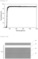
- FIG. 2 illustrates transmittance curve of the insulating layer according to the range of the wavelength. Referring to FIG. 2 , it can be ascertained that the transmittance of the insulating layer is maintained to be 80% or more at the wavelength of 400 nm or more.
- the pulsed laser beam may penetrate through the insulating layer and may be emitted in the direction from the insulating layer to the current collecting layer.
- damage to the electrode may be reduced in comparison with a case in which the pulsed laser beam is emitted in a direction from the current collecting layer to the insulating layer.
- the insulating layer may be damaged. More specifically, the electrode tab, which is thicker than the current collecting layer, needs to be melted so that the electrode tab is welded, a high-output pulsed laser beam needs to be emitted to melt the electrode tab, the current collecting layer maybe deformed because the high-output pulsed laser beam is emitted, and the insulating layer may be damaged due to the deformation of the current collecting layer.
- a welding bead may be formed on a surface of the electrode tab, which may degrade performance of the electrode, but in the case in which the pulsed laser beam is emitted in the direction from the insulating layer to the current collecting layer, the formation of the welding bead on the surface of the electrode tab may be minimized.
- the forming of the electrode active material layer may include providing the electrode active material layer on the primer layer, and exposing one region of the primer layer by removing one region of the electrode active material layer.
- FIGS. 3A to 3C illustrate schematic views of the method of welding an electrode tab according to the exemplary embodiment of the present invention.
- FIG. 3A is a view illustrating a state in which an electrode active material layer 40 is provided on a primer layer 30 of an electrode stack 100 including an insulating layer 10, a current collecting layer 20, and the primer layer 30.
- FIG. 3B is a view illustrating a state in which one region of the electrode active material layer 40 is removed and one region of the primer layer 30 is exposed.
- FIG. 3C is a view illustrating a state in which an electrode tab 50 is laminated in the exposed one region of the primer layer 30, and a pulsed laser beam 200 is emitted in a direction from the insulating layer 10 to the current collecting layer 20.
- the one region of the primer layer may be exposed by etching and removing the one region of the electrode active material layer.
- the etching may be performed by applying an etching mask in the one region of the electrode active material layer and removing the one region of the electrode active material layer where the etching mask is not applied.
- the etching may be wet etching or dry etching.
- the wet etching may be performed by etching the one region of the electrode active material layer, where the etching mask is not applied, by using an etching solution, but the method is not limited.
- the etching solution may include at least one of N-methylpyrrolidone (NMP), water, alcohol, dimethyl sulfoxide (DMSO), and acetone, but types of etching solutions are not limited.
- the dry etching may be performed by removing the electrode active material layer by irradiating the pulsed laser beam to the one region of the electrode active material layer where the etching mask is not applied, but the method is not limited.
- an emission condition of the pulsed laser beam emitted during the dry etching may be adjusted within an appropriate range by a user as necessary, and specifically, in a case in which a 50W pulsed laser beam with an IR wavelength is used, an average output density of the pulsed laser beam may be set to 1 MW/cm 2 to 5 MW/cm 2 .
- the forming of the electrode active material layer may include providing the electrode active material layer on the primer layer in a way to expose a region of the primer layer.
- the electrode active material layer may not be provided in one region where the primer layer will be exposed, but the electrode active material layer may be provided in another region where the primer layer will not be exposed.
- a method such as screen printing, offset printing, flexographic printing, inkjet printing, slot die coating, slide coating, or curtain coating may be used, but the method is not limited.
- the welding of the electrode tab and the current collecting layer may include removing the primer layer being in contact with the electrode tab by irradiating with the pulsed laser beam, and welding the electrode tab and the current collecting layer.
- the current collecting layer may be heated, and the primer layer provided on the heated current collecting layer may be vaporized as the heated current collecting layer is deformed, such that the primer layer may be removed.
- the pulsed laser beam may be emitted by being focused on the current collecting layer.
- the pulsed laser beam may be emitted by being focused on an interlayer between the current collecting layer and the insulating layer.
- the current collecting layer may be deformed while absorbing energy of the laser beam, and the primer layer adjacent to the current collecting layer is vaporized as the current collecting layer is deformed, such that the current collecting layer and the electrode tab may be welded.
- a thickness of the primer layer may be 1 ⁇ m to 10 ⁇ m, specifically, 1 ⁇ m to 5 ⁇ m, and more specifically, 1 ⁇ m to 3 ⁇ m.
- the electrode active material layer may be smoothly applied, and bonding force and conductivity of the primer layer may be ensured.
- the primer layer is sufficiently vaporized, such that the electrode tab may be smoothly welded to the current collecting layer.
- a thickness of the current collecting layer may be 5 ⁇ m to 30 ⁇ m. Specifically, the thickness of the current collecting layer may be 5 ⁇ m to 20 ⁇ m, 10 ⁇ m to 30 ⁇ m, or 10 ⁇ m to 20 ⁇ m.
- a thickness of the insulating layer may be 5 ⁇ m to 30 ⁇ m, and specifically, 10 ⁇ m to 20 ⁇ m.
- the thickness of the insulating layer is within the aforementioned range, it is possible to minimize damage to the insulating layer which is caused as energy absorbed by the current collecting layer when irradiating the pulsed laser beam is transmitted to the insulating layer, and it is possible to minimize damage to the insulating layer which is caused as the insulating layer directly absorbs energy by the emission of the pulsed laser beam. As a result, it is possible to provide a rechargeable battery in which deterioration in durability is minimized within the aforementioned range of the thickness of the insulating layer.
- a thickness of the electrode tab may be 80 ⁇ m to 500 ⁇ m, and specifically, 90 ⁇ m to 300 ⁇ m or 100 ⁇ m to 150 ⁇ m. In the case in which the thickness of the electrode tab is within the aforementioned range, it is possible to provide the electrode in which an increase in resistance and a thickness of a battery are minimized.
- a thickness of the electrode active material layer may be 20 ⁇ m to 150 ⁇ m, specifically, 20 ⁇ m to 130 ⁇ m, 40 ⁇ m to 150 ⁇ m, or 40 ⁇ m to 130 ⁇ m, more specifically, 40 ⁇ m to 110 ⁇ m, 70 ⁇ m to 130 ⁇ m, or 70 ⁇ m to 110 ⁇ m, and still more specifically, 90 ⁇ m to 100 ⁇ m.
- the electrode stack may further include a bonding layer between the current collecting layer and the insulating layer. Since the bonding layer is provided, it is possible to prevent the insulating layer from being separated from the current collecting layer.
- a thickness of the bonding layer may be 1 ⁇ m to 5 ⁇ m. In the case in which the thickness of the bonding layer is within the aforementioned range, it is possible to minimize damage to the insulating layer caused by the emission of the laser beam, and it is possible to prevent separation between the current collecting layer and the insulating layer.
- the bonding layer may be provided with a bonding agent known in the art, and types of bonding agents are not limited.
- the pulsed laser beam may be a pulsed laser beam known in the art, and specifically, the pulsed laser beam may be a laser beam in the form of a pulse, that is, a laser beam of which the emission is performed and stopped over time.
- a pulse energy of the pulsed laser beam is 10 mJ to 30 mJ and may be, specifically, 11 mJ to 30 mJ, 10 mJ to 25 mJ, or 11 mJ to 25 mJ, and more specifically, 12 mJ to 25 mJ, 11 mJ to 20 mJ, or 12 mJ to 20 mJ.
- the pulse energy of the pulsed laser beam By adjusting the pulse energy of the pulsed laser beam to be within the aforementioned range, it is possible to minimize damage to the insulating layer. Specifically, by irradiating the pulsed laser beam having pulse energy within the aforementioned range, it is possible to minimize damage to the insulating layer caused by the emission of the pulsed laser beam while performing the welding of the electrode tab.
- the pulse energy of the pulsed laser beam may mean energy outputted when the emission of the pulsed laser beam is performed and stopped once.
- a spot spacing distance of the pulsed laser beam may be 0.15 mm to 0.45 mm, specifically, 0.15 mm to 0.35 mm, 0.17 mm to 0.45 mm, or 0.17 mm to 0.35 mm, and more specifically, 0.2 mm to 0.35 mm, 0.17 mm to 0.25 mm, or 0.2 mm to 0.25 mm.
- the spot spacing distance of the pulsed laser beam, in a longitudinal direction of the electrode is 0.15 mm to 0.45 mm and may be, specifically, 0.15 mm to 0.35 mm, and more specifically, 0.15 mm to 0.25 mm, and the spot spacing distance of the pulsed laser beam, in a width direction of the electrode, is 0.15 mm to 0.35 mm, and may be, specifically, 0.15 mm to 0.25 mm.
- the spot spacing distance of the pulsed laser beam by adjusting the spot spacing distance of the pulsed laser beam to be within the aforementioned range, it is possible to smoothly weld the electrode tab. Specifically, by adjusting the spot spacing distance of the pulsed laser beam to be within the aforementioned range, it is possible to minimize damage to the current collecting layer and the electrode tab, and it is possible to minimize a decrease in tensile strength caused by a decrease in energy of the emitted pulsed laser beam.
- the spot spacing distance (spot align) of the pulsed laser beam may mean a distance between focal points of the emitted pulsed laser beams.
- the longitudinal direction may be a selvage direction and may be perpendicular to a grain direction and a direction in which the insulating layer, the current collecting layer, and the primer layer are provided.
- the width direction may be the grain direction and may be perpendicular to the selvage direction and the direction in which the insulating layer, the current collecting layer, and the primer layer are provided.
- a spot size of the pulsed laser beam may be 50 ⁇ m to 150 ⁇ m, specifically, 50 ⁇ m to 120 ⁇ m, 60 ⁇ m to 150 ⁇ m, or 60 ⁇ m to 120 ⁇ m, and more specifically, 60 ⁇ m to 100 ⁇ m, 80 ⁇ m to 120 ⁇ m, or 80 ⁇ m to 100 ⁇ m.
- a wavelength of the pulsed laser beam may be 400 nm to 1,200 nm.
- a medium of the pulsed laser beam may be a Yb doped fiber made by adding ytterbium to an optical fiber, but types of media are not limited.
- the method of welding the electrode tab may be a method of welding an electrode tab for a cable type rechargeable battery.
- An electrode made by welding an electrode tab according to the exemplary embodiment of the present invention may be used as an electrode for a rechargeable battery.
- the electrode made by welding the electrode tab may be used as a positive electrode and/or a negative electrode for a rechargeable battery.
- the electrode made by welding the electrode tab may be used as an electrode for a cable type rechargeable battery.
- the electrode made by welding the electrode tab according to the exemplary embodiment of the present invention may be used as an internal electrode and/or an external electrode for a cable type rechargeable battery.
- the electrode made by welding the electrode tab may be used as a positive electrode and/or a negative electrode for a cable type rechargeable battery.
- Another exemplary embodiment of the present invention provides a cable type rechargeable battery including: an internal electrode with a separation layer on outer surface thereof; and an external electrode which is spirally provided on an outer surface of the separation layer, in which at least one of the external electrode and the internal electrode is an electrode welded according to the method of welding an electrode tab.
- the internal electrode may include a current collecting layer, and an electrode active material layer formed on one surface of the current collecting layer, and the current collecting layer and the electrode active material layer may be identical to the current collecting layer and the electrode active material layer, respectively, in the method of welding an electrode tab.
- the separation layer may include at least any one of an electrolyte and an insulating film.
- the electrolyte may include at least one of a gel type polymeric electrolyte using polyethylene oxide, polyvinylidene fluoride, polyvinylidene fluoride-hexafluoropropylene, polymethyl methacrylate, polyacrylonitrile, or polyvinyl acetate; and a solid electrolyte using polyethylene oxide, polypropylene oxide, polyethylene imine, polyethylene sulfide, or polyvinyl acetate.
- the electrolyte may further include lithium salt.
- the lithium salt may include at least one of LiCl, LiBr, LiI, LiClO 4 , LiBF 4 , LiB 10 Cl 10 , LiPF 6 , LiCF 3 SO 3 , LiCF 3 CO 2 , LiAsF 6 , LiSbF 6 , LiAlCl 4 , CH 3 SO 3 Li, CF 3 SO 3 Li, (CF 3 SO 2 ) 2 NLi, chloroborane lithium, short chain aliphatic carboxylic acid lithium, and tetra phenyl boric acid lithium.
- the insulating film may be provided with: a porous polymeric substrate manufactured by using polyolefin-based polymer selected from a group consisting of ethylene homopolymer, propylene homopolymer, ethylene-butene copolymer, ethylene-hexene copolymer, and ethylene-methacrylate copolymer; a porous polymeric substrate manufactured by using polymer selected from a group consisting of polyester, polyacetal, polyamide, polycarbonate, polyimide, polyether ether ketone, polyether sulfone, polyphenylene oxide, polyphenylene sulfide, modified polyethylene terephthalate, and polyethylene naphthalate; a porous substrate made of a mixture of inorganic substance particles and binder polymer; or a porous coating layer formed of a mixture of inorganic substance particles and binder polymer on at least one surface of the porous polymeric substrate.
- polyolefin-based polymer selected from a group consisting of ethylene
- PET polyethylene terephthalate
- a thickness of the insulating layer was about 15 ⁇ m, and transmittance of the insulating layer was 90% or more at a wavelength of 400 nm to 1,200 nm.
- a thickness of the current collecting layer was about 20 ⁇ m.
- the primer layer included carbon black and polyvinylidene fluoride (PVDF), and a thickness of the primer layer was about 3 ⁇ m.
- An electrode active material layer including LiCoO 2 was provided on the primer layer included in the electrode stack.
- a length of the electrode active material layer was about 25 mm, a width of the electrode active material layer was about 10 mm, and a thickness of the electrode active material layer was about 95 ⁇ m.
- An etching mask was formed in a partial region of the electrode active material layer, and a partial region of the electrode active material layer where the etching mask was not formed was processed with an N-methylpyrrolidone (NMP) solution, such that the partial region of the electrode active material layer where the etching mask was not formed was removed, and as a result, a partial region of the primer layer was exposed.
- NMP N-methylpyrrolidone
- a pulsed laser beam having pulse energy of 12.5 mJ, a spot spacing distance of 0.2 mm in a longitudinal direction, a spot spacing distance of 0.2 mm in a width direction, and a spot size of about 90 ⁇ m was emitted by being focused onto the aluminum current collecting layer in a direction from the polyethylene terephthalate insulating layer to the aluminum current collecting layer by using a pulsed laser beam emitter (R4 of SPI), thereby welding the electrode tab to the electrode stack.
- R4 of SPI pulsed laser beam emitter
- An electrode tab was welded to an electrode stack by a method identical to the method of Example 1 except that pulse energy was 17.5 mJ.
- An electrode tab was welded to an electrode stack by a method identical to the method of Example 1 except that pulse energy was 25 mJ.
- An electrode tab was welded to an electrode stack by a method identical to the method of Example 1 except that a laser beam having a spot spacing distance of 0.3 mm in a longitudinal direction and a spot spacing distance of 0.2 mm in a width direction was emitted.
- An electrode tab was welded to an electrode stack by a method identical to the method of Example 1 except that a laser beam having a spot spacing distance of 0.4 mm in a longitudinal direction and a spot spacing distance of 0.2 mm in a width direction was emitted.
- An electrode tab was welded to an electrode stack by a method identical to the method of Example 1 except that a laser beam having a spot spacing distance of 0.2 mm in a longitudinal direction and a spot spacing distance of 0.3 mm in a width direction was emitted.
- An electrode tab was welded to an electrode stack by a method identical to the method of Example 1 except that pulse energy was 35 mJ.
- An electrode tab was welded to an electrode stack by a method identical to the method of Example 1 except that pulse energy was 50 mJ.
- An electrode tab was welded to an electrode stack by a method identical to the method of Example 1 except that an ultrasonic wave was emitted under a condition in which an amplitude was 40% and welding time was 1 second by using an ultrasonic emitter (Branson) instead of the pulsed laser beam.
- an ultrasonic emitter Branson
- An electrode tab was welded to an electrode stack by a method identical to the method of Example 1 except that a laser beam having a spot spacing distance of 0.1 mm in a longitudinal direction and a spot spacing distance of 0.2 mm in a width direction was emitted.
- An electrode tab was welded to an electrode stack by a method identical to the method of Example 1 except that a laser beam having a spot spacing distance of 0.2 mm in a longitudinal direction and a spot spacing distance of 0.1 mm in a width direction was emitted.
- Table 1 shows a summary of information of the welding methods according to Examples 1 to 6 and Comparative Examples 1 to 5.
- Example 1 12.5 0.2 ⁇ 0.2 - Example 2 17.5 0.2 ⁇ 0.2 - Example 3 25 0.2 ⁇ 0.2 - Example 4 12.5 0.3 ⁇ 0.2 - Example 5 12.5 0.4 ⁇ 0.2 - Example 6 12.5 0.2 ⁇ 0.3 - Comparative Example 1 35 0.2 ⁇ 0.2 - Comparative Example 2 50 0.2 ⁇ 0.2 - Comparative Example 3 - - Ultrasonic Welding Comparative Example 4 12.5 0.1 ⁇ 0.2 - Comparative Example 5 12.5 0.2 ⁇ 0.1 -
- Table 2 shows tensile strength values which are measured when each of the electrodes for a rechargeable battery, which have the welded electrode tabs and are manufactured according to Examples 1 to 3 and Comparative Examples 1 to 3, is fractured by extending each of the electrodes in the longitudinal direction at a tension speed of 10 mm/min.
- Table 3 shows tensile strength values which are measured when each of the electrodes for a rechargeable battery, which have the electrode tabs welded according to Examples 1, 4 and 5 and Comparative Example 4, is fractured by extending each of the electrodes in the longitudinal direction at a tension speed of 10 mm/min.
- Table 4 shows tensile strength values which are measured when each of the electrodes for a rechargeable battery, which have the electrode tabs welded according to Examples 1 and 6 and Comparative Example 5, is fractured by extending each of the electrodes in the longitudinal direction at a tension speed of 10 mm/min.
- Table 2 shows tensile strength of the electrodes for a rechargeable battery welded while changing pulse energy of pulsed laser beams.
- the tensile strength needs to have a value approximate to 1 kgf so that the electrode may be applied to the cable type rechargeable battery.
- the tensile strength value is a value that may be applied to the cable type rechargeable battery, but the electrode cannot be applied to the cable type rechargeable battery due to damage to the insulating layer.
- the pulsed laser beam needs to be used to minimize contamination of the electrode caused by the damage to the current collecting layer and the insulating layer.
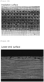
- FIG. 4A is a view illustrating an image captured by using an optical microscope at an irradiation surface of the electrode welded according to Example 1
- FIG. 4B is a view illustrating an image captured by using an optical microscope at a lower end surface of the electrode welded according to Example 1.
- FIG. 5A is a view illustrating an image captured by using an optical microscope at an irradiation surface of the electrode welded according to Comparative Example 2
- FIG. 5B is a view illustrating an image captured by using an optical microscope at a lower end surface of the electrode welded according to Comparative Example 2.
- the insulating layer and the current collecting layer at the irradiation surface and the lower end surface of the electrode according to Example 1 in which the pulsed laser beam having pulse energy of 12.5 mJ are emitted are less damaged, but the electrode is contaminated due to damage to the insulating layer and the current collecting layer at the irradiation surface and the lower end surface of the electrode according to Comparative Example 2 in which the pulsed laser beam having pulse energy of 50 mJ is emitted.
- Tables 3 and 4 show tensile strength of the electrodes for a rechargeable battery which are welded by the pulsed laser beams of which the spot spacing distances vary. According to Tables 2 and 3, it can be ascertained that the tensile strength of the electrode, which is made by irradiating the pulsed laser beam under a condition in which the spot spacing distance in the longitudinal direction is 0.2 mm to 0.4 mm and the spot spacing distance in the width direction is 0.2 mm to 0.3 mm, may be applied to the cable type rechargeable battery, and it can be ascertained that in the case of Comparative Examples 4 and 5 having conditions deviating from the aforementioned condition, the electrodes have the tensile strength value that may be applied to the cable type rechargeable battery, but the electrodes cannot be applied to the cable type rechargeable battery due to damage to the insulating layers.
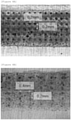
- FIG. 6A is a view illustrating an image showing a spot spacing distance which is captured by using an optical microscope at the irradiation surface of the electrode welded according to Example 1
- FIG. 6B is a view illustrating an image showing a spot spacing distance which is captured by using an optical microscope at the irradiation surface of the electrode welded according to Example 5
- FIG. 6C is a view illustrating an image showing a spot spacing distance which is captured by using an optical microscope at the irradiation surface of the electrode welded according to Example 6.
- the insulating layer and the current collecting layer may be minimized by irradiating the pulsed laser beam having the spot spacing distance within the range according to the exemplary embodiment of the present invention, and the manufactured electrode may have a tensile strength value that may be applied to the cable type rechargeable battery.
Landscapes
- Engineering & Computer Science (AREA)
- Chemical & Material Sciences (AREA)
- Optics & Photonics (AREA)
- Physics & Mathematics (AREA)
- Chemical Kinetics & Catalysis (AREA)
- General Chemical & Material Sciences (AREA)
- Electrochemistry (AREA)
- Mechanical Engineering (AREA)
- Plasma & Fusion (AREA)
- Manufacturing & Machinery (AREA)
- Materials Engineering (AREA)
- Composite Materials (AREA)
- Connection Of Batteries Or Terminals (AREA)
- Battery Electrode And Active Subsutance (AREA)
- Laser Beam Processing (AREA)
- Secondary Cells (AREA)
Description
- The present invention relates to a method of welding an electrode tab and a cable type rechargeable battery including an electrode manufactured according to the same.
- A rechargeable battery refers to a device that converts external electrical energy into chemical energy, stores the chemical energy, and generates electricity when the electricity is required. The rechargeable battery has both economic advantages and environmental advantages compared to a primary battery used as a disposable battery.
- An electrode for a rechargeable battery is configured such that an insulating layer, a current collecting layer, a primer layer, and an electrode active material layer are sequentially provided. Further, to allow the electrode to be actually used for the rechargeable battery, an electrode tab needs to be welded to the current collecting layer so that an electric current may be moved to the outside of the electrode.
- However, there is a problem in that welding quality deteriorates due to contamination caused by the electrode active material layer and the insulating layer during the process of welding the electrode, and as a result, welding needs to be performed after completely removing the electrode active material layer and the insulating layer in order to solve the problem of the contamination of the electrode.
- However, the removal of the insulating layer according to the aforementioned method causes a problem in that flexibility and durability deteriorate such that the electrode cannot be used for a cable type battery.
- Accordingly, there is a need for multifarious researches for minimizing deterioration in weld quality caused by contamination resulting from the welding of the electrode tab and for diversifying welding methods and conditions in order to simplify electrode manufacturing processes.
-
Japanese Patent Application Laid-Open No. 2005-129497 -
DE 10 2012 221 780 A1 -
US 2004/079738 A1 describes a process for producing a lead-acid battery. A lead bushing cast in a lid of an assembled lead-acid battery and a pole inserted through an insertion hole in the lead bushing are welded together by applying a laser beam thereto. At the time of the laser welding, as desired, a jig is placed around the lead bushing so as to surround it and the laser welding is carried out. -
KR 2015 0045388 A -
JP 2015 015147 A -
JP 2005 129497 A - The present invention provides a method of welding an electrode tab and a cable type rechargeable battery including an electrode manufactured according to the same.
- The technical problems from the background art are solved by the present invention as defined by the subject matter of the independent claims. Relevant embodiments of the present invention are defined by the features of the dependent claims.
- A method of welding an electrode tab includes: preparing an electrode stack with an insulating layer, a current collecting layer, and a primer layer, sequentially provided; forming an electrode active material layer which is provided on the primer layer and has a region to which the primer layer is exposed; laminating an electrode tab in the region to which the primer layer is exposed; and welding the electrode tab and the current collecting layer by irradiating a pulsed laser beam, in which transmittance of the insulating layer is 50% or more at a wavelength of 400 nm to 1,200 nm, and the pulsed laser beam penetrates through the insulating layer and is emitted in a direction from the insulating layer to the current collecting layer.
- A cable type rechargeable battery includes: an internal electrode with a separation layer on outer surface thereof; and an external electrode which is spirally provided on an outer surface of the separation layer, in which at least one of the external electrode and the internal electrode is an electrode welded according to the method of welding an electrode tab.
- The method of welding an electrode tab according to the exemplary embodiment of the present invention does not include a process of removing the insulating layer and the primer layer, and as a result, there is an advantage in that the process of welding an electrode tab and the process of manufacturing an electrode are simplified.
- In addition, the method of welding an electrode tab according to the exemplary embodiment of the present invention has an advantage in that damage to the insulating layer is minimized and flexibility and durability of the electrode are ensured.
- The method of welding an electrode tab according to the exemplary embodiment of the present invention has an advantage in that welding quality may be improved by irradiating a pulsed laser beam and adjusting a condition thereof.
-
-
FIG. 1 is a view illustrating digital images of an electrode specimen manufactured by ultrasonic welding. -
FIG. 2 is a view illustrating a transmittance curve in accordance with a wavelength range of an insulating layer included in an electrode stack according to an exemplary embodiment of the present invention. -
FIGS. 3A to 3C are schematic views illustrating a method of welding an electrode tab according to the exemplary embodiment of the present invention. -
FIG. 4A is a view illustrating an image captured by using an optical microscope at an irradiation surface of an electrode welded according to Example 1. -
FIG. 4B is a view illustrating an image captured by using an optical microscope at a lower end surface of the electrode welded according to Example 1. -
FIG. 5A is a view illustrating an image captured by using an optical microscope at an irradiation surface of an electrode welded according to Comparative Example 2. -
FIG. 5B is a view illustrating an image captured by using an optical microscope at a lower end surface of the electrode welded according to Comparative Example 2. -
FIG. 6A is a view illustrating an image which shows a spot spacing distance and is captured by using an optical microscope at the irradiation surface of the electrode welded according to Example 1. -
FIG. 6B is a view illustrating an image which shows a spot spacing distance and is captured by using an optical microscope at an irradiation surface of an electrode welded according to Example 5. -
FIG. 6C is a view illustrating an image which shows a spot spacing distance and is captured by using an optical microscope at an irradiation surface of an electrode welded according to Example 6. - When one member is disposed "on" another member in the present specification, this includes not only a case where the one member is brought into contact with another member, but also a case where still another member is present between the two members.
- When one part "includes" one constituent element in the present specification, unless otherwise specifically described, this does not mean that another constituent element is excluded, but means that another constituent element may be further included.
- Throughout the specification of the present application, the term "transmittance" means a ratio of the amount of light penetrating through a member to the amount of light entering the member. In this case, the amount of light entering the member and the amount of light penetrating through the member may be measured by using a spectrophotometer (Lambda 950, PerkinElmer, Inc.) or the like.
- The present inventors have ascertained that when ultrasonic vibration is applied to a current collecting layer, welding quality deteriorates if an electrode active material layer, a primer layer, and an insulating layer are not completely removed during a process of welding an electrode tab for manufacturing an electrode for a rechargeable battery. Accordingly, the present inventors have conducted continuous research to solve the aforementioned problems by minimizing the process of removing the respective layers that constitute the electrode for a rechargeable battery and concretely specifying a direction and a condition of laser irradiation, and have developed a method of welding an electrode tab which will be described below.
- Hereinafter, the present specification will be described in more detail.
- An exemplary embodiment of the present invention provides a method of welding an electrode tab, the method including: preparing an electrode stack having an insulating layer, a current collecting layer, and a primer layer, which are sequentially provided; forming an electrode active material layer which is provided on the primer layer and has a region to which the primer layer is exposed; laminating an electrode tab in the region in which the primer layer is exposed; and welding the electrode tab and the current collecting layer by irradiating a pulsed laser beam, in which transmittance of the insulating layer is 50% or more at a wavelength of 400 nm to 1,200 nm, and the pulsed laser beam penetrates through the insulating layer and is emitted in a direction from the insulating layer to the current collecting layer.
- According to the exemplary embodiment of the present invention, the insulating layer may be provided on an outer surface of the current collecting layer in order to protect an electrode from moisture in air and external impact. The insulating layer may be made of typical polymeric resin including a moisture blocking layer, and the polymeric resin may include at least one of polyethylene terephthalate (PET), polyvinyl chloride (PVC), high-density polyethylene (HDPE), and epoxy resin. However, any material is acceptable as long as the material may impart flexibility, and types of polymeric resin are not limited.
- According to the exemplary embodiment of the present invention, the current collecting layer may be made of: stainless steel; aluminum, nickel, titanium, fired carbon, copper; stainless steel surface-treated with carbon, nickel, titanium, or silver; aluminum-cadmium alloy; non-conductive polymer surface-treated with a conductive material; conductive polymer; metal paste including metal powder made of Ni, Al, Au, Ag, Al, Pd/Ag, Cr, Ta, Cu, Ba, or indium tin oxide (ITO); or carbon paste including carbon powder made of graphite, carbon black, or carbon nanotube, but types of materials of the current collecting layer are not limited.
- According to an exemplary embodiment of the present invention, the primer layer may include a conductive material and a binder. Since the primer layer includes the conductive material and the binder, the primer layer may serve as both a conductive layer and a bonding layer on an electrode.
- Specifically, the primer layer may effectively bond the electrode active material layer and the current collecting layer, may reduce resistance of the electrode by improving conductivity of the electrode active material layer, and may prevent deterioration in performance of a battery. Specifically, the primer layer may be provided between the current collecting layer and the electrode active material layer.
- According to the exemplary embodiment of the present invention, the conductive material may include at least one of carbon black, acetylene black, Ketjen black, carbon fiber, carbon nanotube, and graphene, but types of conductive materials are not limited.
- According to the exemplary embodiment of the present invention, the binder may include at least one of polyvinylidene fluoride (PVDF), polyvinylidene fluoride-co-hexafluoropropylene, polyvinylidene fluoride-co-trichloroethylene, polybutyl acrylate, polymethyl methacrylate, polyacrylonitrile, polyvinylpyrrolidone, polyvinylacetate, ethylene-co-vinyl acetate, polyethylene oxide, polyarylate, cellulose acetate, cellulose acetate butyrate, cellulose acetate propionate, cyanoethylpullulan, cyanoethylpolyvinylalcohol, cyanoethylcellulose, cyano-ethylsucrose, pullulan, carboxyl methyl cellulose, styrene-butadiene rubber, acrylonitrile-styrene-butadiene copolymer, and polyimide. However, types of binders are not limited.
- According to the exemplary embodiment of the present invention, the electrode active material layer may be provided on the primer layer, and may have a region in which the primer layer is exposed.
- According to the exemplary embodiment of the present invention, in a case in which the electrode is a negative electrode for a rechargeable battery, the electrode active material layer may include at least one of: natural graphite, artificial graphite, or carbonous materials; metal (Me) such as Si, Sn, Li, Zn, Mg, Cd, Ce, Ni, or Fe; alloys including the aforementioned metal (Me); oxide (MeOx) of the aforementioned metal (Me) or lithium titanium oxide (LTO); and composites made of the aforementioned metal (Me) and carbon.
- According to the exemplary embodiment of the present invention, in a case in which the electrode is a positive electrode for a rechargeable battery, the electrode active material layer may include any one active material particle or a mixture of two or more active material particles selected from a group consisting of LiCoO2, LiNiO2, LiMn2O4, LiCoPO4, LiFePO4, LiNiMnCoO2 and LiNi 1-x-y-zCoxM1yM2zO2 (M1 and M2 are each independently any one selected from a group consisting of Al, Ni, Co, Fe, Mn, V, Cr, Ti, W, Ta, Mg, and Mo, and x, y, and z are each independently an atomic fraction of oxide composition elements, and 0 ≤ x < 0.5, 0 ≤ y < 0.5, 0 ≤ z < 0.5, and x+y+z ≤ 1).
- According to the exemplary embodiment of the present invention, the laminating of the electrode tab in the region to which the primer layer is exposed may include bringing the electrode tab into contact with the region in which the primer layer is exposed.
- According to the exemplary embodiment of the present invention, the electrode tab may be laminated on the electrode stack including the primer layer which is partially exposed to the outside.
- Specifically, a partial region of the primer layer, which corresponds to a region in which the electrode tab is laminated, may be exposed, and the electrode tab may be laminated on the primer layer of which the partial region is exposed.
- According to the exemplary embodiment of the present invention, the electrode tab, which is laminated in the region to which the primer layer is exposed, may be at least one of: stainless steel, aluminum, nickel, titanium, fired carbon, copper; stainless steel surface-treated with carbon, nickel, titanium, or silver; and an aluminum-cadmium alloy, but types of electrode tabs are not limited.
- According to the exemplary embodiment of the present invention, the welding of the electrode tab and the current collecting layer may be performed by irradiating the pulsed laser beam. If the welding is performed by using ultrasonic vibration, an irradiation surface and a lower end surface of the electrode may be contaminated by the electrode active material layer or the insulating layer.
-
FIG. 1 is a view illustrating digital images of an electrode specimen manufactured by ultrasonic welding. Referring toFIG. 1 , a portion where the electrode tab is provided on the electrode may mean the lower end surface, and a portion where the electrode is provided on the electrode tab may mean the irradiation surface. - According to the exemplary embodiment of the present invention, transmittance of the insulating layer may be 50% or more at a wavelength of 400 nm to 1,200 nm. Specifically, transmittance of the insulating layer to light having any one of wavelength values of 400 nm to 1,200 nm may be 50% or more. In addition, transmittance of the insulating layer may be 80% to 95% at a wavelength of 400 nm to 1,200 nm. In the case in which the transmittance of the insulating layer is within the aforementioned range, the pulsed laser beam may penetrate through the insulating layer while minimizing damage to the insulating layer when the pulsed laser beam is emitted in a direction from the insulating layer to the current collecting layer.
-
FIG. 2 illustrates transmittance curve of the insulating layer according to the range of the wavelength. Referring toFIG. 2 , it can be ascertained that the transmittance of the insulating layer is maintained to be 80% or more at the wavelength of 400 nm or more. - According to the exemplary embodiment of the present invention, the pulsed laser beam may penetrate through the insulating layer and may be emitted in the direction from the insulating layer to the current collecting layer.
- In the case in which the pulsed laser beam is emitted in the direction from the insulating layer to the current collecting layer, damage to the electrode may be reduced in comparison with a case in which the pulsed laser beam is emitted in a direction from the current collecting layer to the insulating layer.
- Specifically, in the case in which the pulsed laser beam is emitted in the direction from the current collecting layer to the insulating layer, the insulating layer may be damaged. More specifically, the electrode tab, which is thicker than the current collecting layer, needs to be melted so that the electrode tab is welded, a high-output pulsed laser beam needs to be emitted to melt the electrode tab, the current collecting layer maybe deformed because the high-output pulsed laser beam is emitted, and the insulating layer may be damaged due to the deformation of the current collecting layer.
- In addition, in the case in which the pulsed laser beam is emitted in the direction from the current collecting layer to the insulating layer, a welding bead may be formed on a surface of the electrode tab, which may degrade performance of the electrode, but in the case in which the pulsed laser beam is emitted in the direction from the insulating layer to the current collecting layer, the formation of the welding bead on the surface of the electrode tab may be minimized.
- According to the exemplary embodiment of the present invention, the forming of the electrode active material layer may include providing the electrode active material layer on the primer layer, and exposing one region of the primer layer by removing one region of the electrode active material layer.
-
FIGS. 3A to 3C illustrate schematic views of the method of welding an electrode tab according to the exemplary embodiment of the present invention. Specifically,FIG. 3A is a view illustrating a state in which an electrodeactive material layer 40 is provided on aprimer layer 30 of anelectrode stack 100 including an insulatinglayer 10, acurrent collecting layer 20, and theprimer layer 30.FIG. 3B is a view illustrating a state in which one region of the electrodeactive material layer 40 is removed and one region of theprimer layer 30 is exposed.FIG. 3C is a view illustrating a state in which anelectrode tab 50 is laminated in the exposed one region of theprimer layer 30, and apulsed laser beam 200 is emitted in a direction from the insulatinglayer 10 to thecurrent collecting layer 20. - According to the exemplary embodiment of the present invention, the one region of the primer layer may be exposed by etching and removing the one region of the electrode active material layer. For example, the etching may be performed by applying an etching mask in the one region of the electrode active material layer and removing the one region of the electrode active material layer where the etching mask is not applied.
- According to the exemplary embodiment of the present invention, the etching may be wet etching or dry etching.
- According to the exemplary embodiment of the present invention, the wet etching may be performed by etching the one region of the electrode active material layer, where the etching mask is not applied, by using an etching solution, but the method is not limited. Specifically, the etching solution may include at least one of N-methylpyrrolidone (NMP), water, alcohol, dimethyl sulfoxide (DMSO), and acetone, but types of etching solutions are not limited.
- According to the exemplary embodiment of the present invention, the dry etching may be performed by removing the electrode active material layer by irradiating the pulsed laser beam to the one region of the electrode active material layer where the etching mask is not applied, but the method is not limited.
- According to the exemplary embodiment of the present invention, an emission condition of the pulsed laser beam emitted during the dry etching may be adjusted within an appropriate range by a user as necessary, and specifically, in a case in which a 50W pulsed laser beam with an IR wavelength is used, an average output density of the pulsed laser beam may be set to 1 MW/cm2 to 5 MW/cm2.
- According to the exemplary embodiment of the present invention, the forming of the electrode active material layer may include providing the electrode active material layer on the primer layer in a way to expose a region of the primer layer. Specifically, the electrode active material layer may not be provided in one region where the primer layer will be exposed, but the electrode active material layer may be provided in another region where the primer layer will not be exposed.
- More specifically, as the method of providing the electrode active material layer in the region where the primer layer will not be exposed, a method such as screen printing, offset printing, flexographic printing, inkjet printing, slot die coating, slide coating, or curtain coating may be used, but the method is not limited.
- According to the exemplary embodiment of the present invention, the welding of the electrode tab and the current collecting layer may include removing the primer layer being in contact with the electrode tab by irradiating with the pulsed laser beam, and welding the electrode tab and the current collecting layer.
- Specifically, since the pulsed laser beam is emitted onto the current collecting layer, the current collecting layer may be heated, and the primer layer provided on the heated current collecting layer may be vaporized as the heated current collecting layer is deformed, such that the primer layer may be removed.
- According to an exemplary embodiment of the present invention, the pulsed laser beam may be emitted by being focused on the current collecting layer. Specifically, the pulsed laser beam may be emitted by being focused on an interlayer between the current collecting layer and the insulating layer.
- Since the pulsed laser beam is emitted by being focused on the current collecting layer, the current collecting layer may be deformed while absorbing energy of the laser beam, and the primer layer adjacent to the current collecting layer is vaporized as the current collecting layer is deformed, such that the current collecting layer and the electrode tab may be welded.
- According to the exemplary embodiment of the present invention, a thickness of the primer layer may be 1 µm to 10 µm, specifically, 1 µm to 5 µm, and more specifically, 1 µm to 3 µm. In the case in which the thickness of the primer layer is within the aforementioned range, the electrode active material layer may be smoothly applied, and bonding force and conductivity of the primer layer may be ensured. In addition, as the pulsed laser beam is emitted and absorbed, the primer layer is sufficiently vaporized, such that the electrode tab may be smoothly welded to the current collecting layer.
- According to an exemplary embodiment of the present specification, a thickness of the current collecting layer may be 5 µm to 30 µm. Specifically, the thickness of the current collecting layer may be 5 µm to 20 µm, 10 µm to 30 µm, or 10 µm to 20 µm. By adjusting the thickness of the current collecting layer to be within the aforementioned range, it is possible to minimize damage to the current collecting layer caused by the welding of the electrode tab, and it is possible to sufficiently weld the electrode tab.
- According to the exemplary embodiment of the present invention, a thickness of the insulating layer may be 5 µm to 30 µm, and specifically, 10 µm to 20 µm. By adjusting the thickness of the insulating layer to be within the aforementioned range, it is possible to minimize damage to the electrode caused by the emission of the pulsed laser beam when welding the electrode tab, and it is possible to smoothly weld the electrode tab.
- Specifically, in the case in which the thickness of the insulating layer is within the aforementioned range, it is possible to minimize damage to the insulating layer which is caused as energy absorbed by the current collecting layer when irradiating the pulsed laser beam is transmitted to the insulating layer, and it is possible to minimize damage to the insulating layer which is caused as the insulating layer directly absorbs energy by the emission of the pulsed laser beam. As a result, it is possible to provide a rechargeable battery in which deterioration in durability is minimized within the aforementioned range of the thickness of the insulating layer.
- According to the exemplary embodiment of the present invention, a thickness of the electrode tab may be 80 µm to 500 µm, and specifically, 90 µm to 300 µm or 100 µm to 150 µm. In the case in which the thickness of the electrode tab is within the aforementioned range, it is possible to provide the electrode in which an increase in resistance and a thickness of a battery are minimized.
- According to the exemplary embodiment of the present invention, a thickness of the electrode active material layer may be 20 µm to 150 µm, specifically, 20 µm to 130 µm, 40 µm to 150 µm, or 40 µm to 130 µm, more specifically, 40 µm to 110 µm, 70 µm to 130 µm, or 70 µm to 110 µm, and still more specifically, 90 µm to 100 µm. By adjusting the thickness of the electrode active material layer to be within the aforementioned range, it is possible to provide the electrode having excellent electrical conductivity and a large charging capacity.
- According to the exemplary embodiment of the present invention, the electrode stack may further include a bonding layer between the current collecting layer and the insulating layer. Since the bonding layer is provided, it is possible to prevent the insulating layer from being separated from the current collecting layer.
- According to the exemplary embodiment of the present invention, a thickness of the bonding layer may be 1 µm to 5 µm. In the case in which the thickness of the bonding layer is within the aforementioned range, it is possible to minimize damage to the insulating layer caused by the emission of the laser beam, and it is possible to prevent separation between the current collecting layer and the insulating layer.
- According to the exemplary embodiment of the present invention, the bonding layer may be provided with a bonding agent known in the art, and types of bonding agents are not limited.
- In the present specification, the pulsed laser beam may be a pulsed laser beam known in the art, and specifically, the pulsed laser beam may be a laser beam in the form of a pulse, that is, a laser beam of which the emission is performed and stopped over time.
- A pulse energy of the pulsed laser beam is 10 mJ to 30 mJ and may be, specifically, 11 mJ to 30 mJ, 10 mJ to 25 mJ, or 11 mJ to 25 mJ, and more specifically, 12 mJ to 25 mJ, 11 mJ to 20 mJ, or 12 mJ to 20 mJ.
- By adjusting the pulse energy of the pulsed laser beam to be within the aforementioned range, it is possible to minimize damage to the insulating layer. Specifically, by irradiating the pulsed laser beam having pulse energy within the aforementioned range, it is possible to minimize damage to the insulating layer caused by the emission of the pulsed laser beam while performing the welding of the electrode tab.
- In the present specification, the pulse energy of the pulsed laser beam may mean energy outputted when the emission of the pulsed laser beam is performed and stopped once.
- According to the exemplary embodiment of the present invention, a spot spacing distance of the pulsed laser beam may be 0.15 mm to 0.45 mm, specifically, 0.15 mm to 0.35 mm, 0.17 mm to 0.45 mm, or 0.17 mm to 0.35 mm, and more specifically, 0.2 mm to 0.35 mm, 0.17 mm to 0.25 mm, or 0.2 mm to 0.25 mm.
- The spot spacing distance of the pulsed laser beam, in a longitudinal direction of the electrode, is 0.15 mm to 0.45 mm and may be, specifically, 0.15 mm to 0.35 mm, and more specifically, 0.15 mm to 0.25 mm, and the spot spacing distance of the pulsed laser beam, in a width direction of the electrode, is 0.15 mm to 0.35 mm, and may be, specifically, 0.15 mm to 0.25 mm.
- According to the exemplary embodiment of the present invention, by adjusting the spot spacing distance of the pulsed laser beam to be within the aforementioned range, it is possible to smoothly weld the electrode tab. Specifically, by adjusting the spot spacing distance of the pulsed laser beam to be within the aforementioned range, it is possible to minimize damage to the current collecting layer and the electrode tab, and it is possible to minimize a decrease in tensile strength caused by a decrease in energy of the emitted pulsed laser beam.
- In the present specification, the spot spacing distance (spot align) of the pulsed laser beam may mean a distance between focal points of the emitted pulsed laser beams.
- In the present specification, the longitudinal direction may be a selvage direction and may be perpendicular to a grain direction and a direction in which the insulating layer, the current collecting layer, and the primer layer are provided.
- In the present specification, the width direction may be the grain direction and may be perpendicular to the selvage direction and the direction in which the insulating layer, the current collecting layer, and the primer layer are provided.
- According to the exemplary embodiment of the present invention, a spot size of the pulsed laser beam may be 50 µm to 150 µm, specifically, 50 µm to 120 µm, 60 µm to 150 µm, or 60 µm to 120 µm, and more specifically, 60 µm to 100 µm, 80 µm to 120 µm, or 80 µm to 100 µm.
- According to the exemplary embodiment of the present invention, a wavelength of the pulsed laser beam may be 400 nm to 1,200 nm.
- According to the exemplary embodiment of the present invention, a medium of the pulsed laser beam may be a Yb doped fiber made by adding ytterbium to an optical fiber, but types of media are not limited.
- According to the exemplary embodiment of the present invention, the method of welding the electrode tab may be a method of welding an electrode tab for a cable type rechargeable battery.
- An electrode made by welding an electrode tab according to the exemplary embodiment of the present invention may be used as an electrode for a rechargeable battery. Specifically, the electrode made by welding the electrode tab may be used as a positive electrode and/or a negative electrode for a rechargeable battery. In addition, the electrode made by welding the electrode tab may be used as an electrode for a cable type rechargeable battery.
- The electrode made by welding the electrode tab according to the exemplary embodiment of the present invention may be used as an internal electrode and/or an external electrode for a cable type rechargeable battery. In addition, the electrode made by welding the electrode tab may be used as a positive electrode and/or a negative electrode for a cable type rechargeable battery.
- Another exemplary embodiment of the present invention provides a cable type rechargeable battery including: an internal electrode with a separation layer on outer surface thereof; and an external electrode which is spirally provided on an outer surface of the separation layer, in which at least one of the external electrode and the internal electrode is an electrode welded according to the method of welding an electrode tab.
- According to the exemplary embodiment of the present invention, the internal electrode may include a current collecting layer, and an electrode active material layer formed on one surface of the current collecting layer, and the current collecting layer and the electrode active material layer may be identical to the current collecting layer and the electrode active material layer, respectively, in the method of welding an electrode tab.
- According to the exemplary embodiment of the present invention, the separation layer may include at least any one of an electrolyte and an insulating film.
- According to the exemplary embodiment of the present invention, the electrolyte may include at least one of a gel type polymeric electrolyte using polyethylene oxide, polyvinylidene fluoride, polyvinylidene fluoride-hexafluoropropylene, polymethyl methacrylate, polyacrylonitrile, or polyvinyl acetate; and a solid electrolyte using polyethylene oxide, polypropylene oxide, polyethylene imine, polyethylene sulfide, or polyvinyl acetate.
- In addition, the electrolyte may further include lithium salt. The lithium salt may include at least one of LiCl, LiBr, LiI, LiClO4, LiBF4, LiB10Cl10, LiPF6, LiCF3SO3, LiCF3CO2, LiAsF6, LiSbF6, LiAlCl4, CH3SO3Li, CF3SO3Li, (CF3SO2)2NLi, chloroborane lithium, short chain aliphatic carboxylic acid lithium, and tetra phenyl boric acid lithium.
- According to the exemplary embodiment of the present invention, the insulating film may be provided with: a porous polymeric substrate manufactured by using polyolefin-based polymer selected from a group consisting of ethylene homopolymer, propylene homopolymer, ethylene-butene copolymer, ethylene-hexene copolymer, and ethylene-methacrylate copolymer; a porous polymeric substrate manufactured by using polymer selected from a group consisting of polyester, polyacetal, polyamide, polycarbonate, polyimide, polyether ether ketone, polyether sulfone, polyphenylene oxide, polyphenylene sulfide, modified polyethylene terephthalate, and polyethylene naphthalate; a porous substrate made of a mixture of inorganic substance particles and binder polymer; or a porous coating layer formed of a mixture of inorganic substance particles and binder polymer on at least one surface of the porous polymeric substrate.
- Hereinafter, the present invention will be described in detail with reference to Examples for specifically describing the present invention. However, the Examples according to the present invention may be modified in various forms, and it is not interpreted that the scope of the present invention is limited to the Examples to be described below. The Examples of the present specification are provided for more completely explaining the present invention to the person with ordinary skill in the art.
- An electrode stack having a polyethylene terephthalate (PET) insulating layer, an aluminum current collecting layer, and a primer layer, sequentially provided, was prepared.
- A thickness of the insulating layer was about 15 µm, and transmittance of the insulating layer was 90% or more at a wavelength of 400 nm to 1,200 nm. A thickness of the current collecting layer was about 20 µm. The primer layer included carbon black and polyvinylidene fluoride (PVDF), and a thickness of the primer layer was about 3 µm.
- An electrode active material layer including LiCoO2 was provided on the primer layer included in the electrode stack. A length of the electrode active material layer was about 25 mm, a width of the electrode active material layer was about 10 mm, and a thickness of the electrode active material layer was about 95 µm.
- An etching mask was formed in a partial region of the electrode active material layer, and a partial region of the electrode active material layer where the etching mask was not formed was processed with an N-methylpyrrolidone (NMP) solution, such that the partial region of the electrode active material layer where the etching mask was not formed was removed, and as a result, a partial region of the primer layer was exposed.
- An aluminum electrode tab having a length of 20 mm, a width of 1.5 mm, and a thickness of 100 µm was laminated on the partially exposed part of the primer layer.
- A pulsed laser beam having pulse energy of 12.5 mJ, a spot spacing distance of 0.2 mm in a longitudinal direction, a spot spacing distance of 0.2 mm in a width direction, and a spot size of about 90 µm was emitted by being focused onto the aluminum current collecting layer in a direction from the polyethylene terephthalate insulating layer to the aluminum current collecting layer by using a pulsed laser beam emitter (R4 of SPI), thereby welding the electrode tab to the electrode stack.
- An electrode tab was welded to an electrode stack by a method identical to the method of Example 1 except that pulse energy was 17.5 mJ.
- An electrode tab was welded to an electrode stack by a method identical to the method of Example 1 except that pulse energy was 25 mJ.
- An electrode tab was welded to an electrode stack by a method identical to the method of Example 1 except that a laser beam having a spot spacing distance of 0.3 mm in a longitudinal direction and a spot spacing distance of 0.2 mm in a width direction was emitted.
- An electrode tab was welded to an electrode stack by a method identical to the method of Example 1 except that a laser beam having a spot spacing distance of 0.4 mm in a longitudinal direction and a spot spacing distance of 0.2 mm in a width direction was emitted.
- An electrode tab was welded to an electrode stack by a method identical to the method of Example 1 except that a laser beam having a spot spacing distance of 0.2 mm in a longitudinal direction and a spot spacing distance of 0.3 mm in a width direction was emitted.
- An electrode tab was welded to an electrode stack by a method identical to the method of Example 1 except that pulse energy was 35 mJ.
- An electrode tab was welded to an electrode stack by a method identical to the method of Example 1 except that pulse energy was 50 mJ.
- An electrode tab was welded to an electrode stack by a method identical to the method of Example 1 except that an ultrasonic wave was emitted under a condition in which an amplitude was 40% and welding time was 1 second by using an ultrasonic emitter (Branson) instead of the pulsed laser beam.
- An electrode tab was welded to an electrode stack by a method identical to the method of Example 1 except that a laser beam having a spot spacing distance of 0.1 mm in a longitudinal direction and a spot spacing distance of 0.2 mm in a width direction was emitted.
- An electrode tab was welded to an electrode stack by a method identical to the method of Example 1 except that a laser beam having a spot spacing distance of 0.2 mm in a longitudinal direction and a spot spacing distance of 0.1 mm in a width direction was emitted.
- The following Table 1 shows a summary of information of the welding methods according to Examples 1 to 6 and Comparative Examples 1 to 5.
[Table 1] Items Pulse Energy (mJ) Spot Spacing Distance (Longitudinal Direction mm × Width Direction mm) Remarks Example 1 12.5 0.2 × 0.2 - Example 2 17.5 0.2 × 0.2 - Example 3 25 0.2 × 0.2 - Example 4 12.5 0.3 × 0.2 - Example 5 12.5 0.4 × 0.2 - Example 6 12.5 0.2 × 0.3 - Comparative Example 1 35 0.2 × 0.2 - Comparative Example 2 50 0.2 × 0.2 - Comparative Example 3 - - Ultrasonic Welding Comparative Example 4 12.5 0.1 × 0.2 - Comparative Example 5 12.5 0.2 × 0.1 - - The following Table 2 shows tensile strength values which are measured when each of the electrodes for a rechargeable battery, which have the welded electrode tabs and are manufactured according to Examples 1 to 3 and Comparative Examples 1 to 3, is fractured by extending each of the electrodes in the longitudinal direction at a tension speed of 10 mm/min.
- The following Table 3 shows tensile strength values which are measured when each of the electrodes for a rechargeable battery, which have the electrode tabs welded according to Examples 1, 4 and 5 and Comparative Example 4, is fractured by extending each of the electrodes in the longitudinal direction at a tension speed of 10 mm/min.
- The following Table 4 shows tensile strength values which are measured when each of the electrodes for a rechargeable battery, which have the electrode tabs welded according to Examples 1 and 6 and Comparative Example 5, is fractured by extending each of the electrodes in the longitudinal direction at a tension speed of 10 mm/min.
[Table 2] Items Pulse Energy (mJ) Spot Spacing Distance (Longitudinal Direction mm × Width Direction mm) Tensile Strength (kgf) Example 1 12.5 0.2 × 0.2 1.17 Example 2 17.5 0.2 × 0.2 1.09 Example 3 25 0.2 × 0.2 0.92 Comparative Example 1 35 0.2 × 0.2 0.68 Comparative Example 2 50 0.2 × 0.2 0.63 Comparative Example 3 Ultrasonic Welding 1.01 [Table 3] Items Pulse Energy (mJ) Spot Spacing Distance (Longitudinal Direction mm × Width Direction mm) Tensile Strength (kgf) Example 1 12.5 0.2 × 0.2 1.17 Example 4 12.5 0.3 × 0.2 1.14 Example 5 12.5 0.4 × 0.2 1.05 Comparative Example 4 12.5 0.1 × 0.2 0.99 [Table 4] Items Pulse Energy (mJ) Spot Spacing Distance (Longitudinal Direction mm × Width Direction mm) Tensile Strength (kgf) Example 1 12.5 0.2 × 0.2 1.17 Example 6 12.5 0.2 × 0.3 1.05 Comparative Example 5 12.5 0.2 × 0.1 1.13 - Images of irradiation surfaces of the electrodes for a rechargeable battery, which had the electrode tabs welded according to Examples 1, 5, and 6 and Comparative Example 2, were captured by using an optical microscope (Olympus BX51M).
- Images of lower end surfaces of the electrodes for a rechargeable battery, which had the electrode tabs welded according to Example 1 and Comparative Example 2, were captured by using an optical microscope (Olympus BX51M).
- Table 2 shows tensile strength of the electrodes for a rechargeable battery welded while changing pulse energy of pulsed laser beams. The tensile strength needs to have a value approximate to 1 kgf so that the electrode may be applied to the cable type rechargeable battery.
- According to Table 2, it can be ascertained that the electrodes according to Examples 1 to 3 may be applied to the cable type rechargeable battery, but the electrodes according to Comparative Examples 1 and 2 cannot be applied to the cable type rechargeable battery.
- In addition, it can be ascertained that in the case of Comparative Example 3 in which the electrode tab is welded by ultrasonic welding, the tensile strength value is a value that may be applied to the cable type rechargeable battery, but the electrode cannot be applied to the cable type rechargeable battery due to damage to the insulating layer.
- Further, it can be ascertained that in a case in which the electrode is welded by using ultrasonic waves, the current collecting layer and the insulating layer are damaged, and as a result, the pulsed laser beam needs to be used to minimize contamination of the electrode caused by the damage to the current collecting layer and the insulating layer.
-
FIG. 4A is a view illustrating an image captured by using an optical microscope at an irradiation surface of the electrode welded according to Example 1, andFIG. 4B is a view illustrating an image captured by using an optical microscope at a lower end surface of the electrode welded according to Example 1. -
FIG. 5A is a view illustrating an image captured by using an optical microscope at an irradiation surface of the electrode welded according to Comparative Example 2, andFIG. 5B is a view illustrating an image captured by using an optical microscope at a lower end surface of the electrode welded according to Comparative Example 2. - According to
FIGS. 4A, 4B ,5A, and 5B , it can be ascertained that the insulating layer and the current collecting layer at the irradiation surface and the lower end surface of the electrode according to Example 1 in which the pulsed laser beam having pulse energy of 12.5 mJ are emitted, are less damaged, but the electrode is contaminated due to damage to the insulating layer and the current collecting layer at the irradiation surface and the lower end surface of the electrode according to Comparative Example 2 in which the pulsed laser beam having pulse energy of 50 mJ is emitted. - Collectively, it can be ascertained that when the pulsed laser beam having pulse energy within the range according to the exemplary embodiment of the present invention is emitted, damage to the insulating layer and the current collecting layer may be minimized, and the electrode may have the tensile strength value which may be applied to the cable type rechargeable battery.
- Tables 3 and 4 show tensile strength of the electrodes for a rechargeable battery which are welded by the pulsed laser beams of which the spot spacing distances vary. According to Tables 2 and 3, it can be ascertained that the tensile strength of the electrode, which is made by irradiating the pulsed laser beam under a condition in which the spot spacing distance in the longitudinal direction is 0.2 mm to 0.4 mm and the spot spacing distance in the width direction is 0.2 mm to 0.3 mm, may be applied to the cable type rechargeable battery, and it can be ascertained that in the case of Comparative Examples 4 and 5 having conditions deviating from the aforementioned condition, the electrodes have the tensile strength value that may be applied to the cable type rechargeable battery, but the electrodes cannot be applied to the cable type rechargeable battery due to damage to the insulating layers.
-
FIG. 6A is a view illustrating an image showing a spot spacing distance which is captured by using an optical microscope at the irradiation surface of the electrode welded according to Example 1,FIG. 6B is a view illustrating an image showing a spot spacing distance which is captured by using an optical microscope at the irradiation surface of the electrode welded according to Example 5, andFIG. 6C is a view illustrating an image showing a spot spacing distance which is captured by using an optical microscope at the irradiation surface of the electrode welded according to Example 6. - According to
FIGS. 6A, 6B , and6C , it can be ascertained that damage, which is caused, by a leak of the current collecting layer, to the irradiation surfaces of the electrodes according to Examples 1, 5, and 6 in which the pulsed laser beam is emitted under the condition in which the spot spacing distance in the longitudinal direction is 0.2 mm to 0.4mm and the spot spacing distance in the width direction is 0.2 mm to 0.3 mm, is minimized - Collectively, it can be ascertained that damage to the insulating layer and the current collecting layer may be minimized by irradiating the pulsed laser beam having the spot spacing distance within the range according to the exemplary embodiment of the present invention, and the manufactured electrode may have a tensile strength value that may be applied to the cable type rechargeable battery.
-
- 10:
- Insulating layer
- 20:
- Current collecting layer
- 30:
- Primer layer
- 40:
- Electrode active material layer
- 50:
- Electrode tab
- 100:
- Electrode stack
- 200:
- Pulsed laser beam
Claims (13)
- A method of welding an electrode tab, the method comprising:preparing an electrode stack (100) with an insulating layer (10), a current collecting layer (20), and a primer layer (30), sequentially provided;forming an electrode active material layer (40) which is provided on the primer layer (30) and has a region in which the primer layer (30) is exposed;laminating an electrode tab (50) in the region in which the primer layer (30) is exposed; andwelding the electrode tab (50) and the current collecting layer (20) by irradiating a pulsed laser beam,wherein transmittance of the insulating layer (10) is 50% or more at a wavelength of 400 nm to 1,200 nm, and the pulsed laser beam penetrates through the insulating layer (10) and is emitted in a direction from the insulating layer (10) to the current collecting layer (20),wherein pulse energy of the pulsed laser beam is 10 mJ to 30 mJ,wherein a spot spacing distance of the pulsed laser beam in a longitudinal direction is 0.15 mm to 0.45 mm, andwherein a spot spacing distance of the pulsed laser beam in a width direction of the electrode is 0.15 mm to 0.35 mm.
- The method of claim 1, wherein the forming of the electrode active material layer (40) includes providing the electrode active material layer (40) on the primer layer (30), and exposing one region of the primer layer (30) by removing one region of the electrode active material layer (40).
- The method of claim 1, wherein the forming of the electrode active material layer (40) includes providing the electrode active material layer (40) on the primer layer (30) in a way to expose a region of the primer layer (30).
- The method of claim 1, wherein the welding of the electrode tab (50) and the current collecting layer (20) includes removing the primer layer (30) in contact with the electrode tab (50) by irradiating the pulsed laser beam, and welding the electrode tab (50) and the current collecting layer (20).
- The method of claim 1, wherein the pulsed laser beam is emitted by being focused on the current collecting layer (20).
- The method of claim 1, wherein a thickness of the primer layer (30) is 1 µm to 10 µm.
- The method of claim 1, wherein a thickness of the current collecting layer (20) is 5 µm to 30 µm, and wherein a thickness of the insulating layer (10) is 5 µm to 30 µm.
- The method of claim 1, wherein a thickness of the electrode tab (50) is 80 µm to 500 µm.
- The method of claim 1, wherein a thickness of the electrode active material layer (40) is 20 µm to 150 µm.
- The method of claim 1, wherein the electrode stack further includes a bonding layer between the current collecting layer (20) and the insulating layer (10), and wherein a thickness of the bonding layer is 1 µm to 5 µm.
- The method of claim 1, wherein a spot size of the pulsed laser beam is 50 µm to 150 µm, and wherein a wavelength of the pulsed laser beam is 400 nm to 1,200 nm.
- The method of claim 1, wherein the method of welding an electrode tab (50) is a method of welding an electrode tab (50) for a cable type rechargeable battery.
- A cable type rechargeable battery comprising:an internal electrode with a separation layer on outer surface thereof; andan external electrode which is spirally provided on an outer surface of the separation layer,wherein at least one of the external electrode and the internal electrode is an electrode welded according to the method of welding an electrode tab according to claim 1.
Applications Claiming Priority (2)
| Application Number | Priority Date | Filing Date | Title |
|---|---|---|---|
| KR1020170081403A KR102155029B1 (en) | 2017-06-27 | 2017-06-27 | Welding method of electrode tap and cable-type secondary battery comprising electrode welded by the same |
| PCT/KR2018/007268 WO2019004719A1 (en) | 2017-06-27 | 2018-06-27 | Method for welding electrode tab and cable-type secondary battery comprising electrode manufactured thereby |
Publications (3)
| Publication Number | Publication Date |
|---|---|
| EP3648199A1 EP3648199A1 (en) | 2020-05-06 |
| EP3648199A4 EP3648199A4 (en) | 2020-06-17 |
| EP3648199B1 true EP3648199B1 (en) | 2022-02-23 |
Family
ID=64742452
Family Applications (1)
| Application Number | Title | Priority Date | Filing Date |
|---|---|---|---|
| EP18825259.7A Active EP3648199B1 (en) | 2017-06-27 | 2018-06-27 | Method for welding electrode tab and cable-type secondary battery comprising electrode manufactured thereby |
Country Status (6)
| Country | Link |
|---|---|
| US (1) | US11355821B2 (en) |
| EP (1) | EP3648199B1 (en) |
| JP (1) | JP6966037B2 (en) |
| KR (1) | KR102155029B1 (en) |
| CN (1) | CN110731024B (en) |
| WO (1) | WO2019004719A1 (en) |
Families Citing this family (8)
| Publication number | Priority date | Publication date | Assignee | Title |
|---|---|---|---|---|
| KR102364463B1 (en) * | 2018-08-08 | 2022-02-16 | 주식회사 엘지에너지솔루션 | Electrode for lithium secondary battery and lithium secondary battery including the same |
| US11890705B2 (en) * | 2018-11-13 | 2024-02-06 | Rivian Ip Holdings, Llc | Weld location detection in a battery cell pack |
| CN111682154B (en) * | 2020-06-19 | 2023-01-24 | 珠海冠宇电池股份有限公司 | Tab welding structure, battery and electronic product |
| CN111682156B (en) * | 2020-06-19 | 2023-06-30 | 珠海冠宇电池股份有限公司 | Battery and its preparation method and electronic product |
| CN111682155A (en) * | 2020-06-19 | 2020-09-18 | 珠海冠宇电池股份有限公司 | Batteries and portable electrical equipment |
| CN111682158B (en) * | 2020-06-19 | 2022-11-01 | 珠海冠宇电池股份有限公司 | Tab welding structure, battery and electronic product |
| US20240399498A1 (en) * | 2021-09-28 | 2024-12-05 | Panasonic Intellectual Property Management Co., Ltd. | Welding method and welding structure of metal member |
| KR20230077053A (en) * | 2021-11-25 | 2023-06-01 | 주식회사 엘지에너지솔루션 | Battery for short circuit testing and the preparation method thereof and battery safety analysis method using the same |
Family Cites Families (16)
| Publication number | Priority date | Publication date | Assignee | Title |
|---|---|---|---|---|
| KR19980037992A (en) | 1996-11-22 | 1998-08-05 | 손욱 | How to attach the positive electrode tab of the battery |
| JP4184663B2 (en) * | 1999-10-28 | 2008-11-19 | 古河電池株式会社 | Manufacturing method of lead-acid battery and jig for manufacturing the same |
| JP2005129497A (en) | 2003-09-30 | 2005-05-19 | Sanyo Electric Co Ltd | Electrode plate for alkaline storage battery, method for producing the same, and alkaline storage battery |
| DE102010062140B4 (en) | 2010-11-29 | 2014-04-03 | Zentrum für Sonnenenergie- und Wasserstoff-Forschung Baden-Württemberg Gemeinnützige Stiftung | Battery electrode and method of making same, as well as battery |
| JP2012213789A (en) * | 2011-03-31 | 2012-11-08 | Sanyo Electric Co Ltd | Laser welding method and battery made by the laser welding method |
| WO2013001821A1 (en) | 2011-06-28 | 2013-01-03 | 日本ケミコン株式会社 | Electricity storage device and method for manufacturing electricity storage device |
| EP2892103B1 (en) * | 2012-08-29 | 2018-02-14 | Showa Denko K.K. | Electricity storage device and method for producing same |
| DE102012221780A1 (en) * | 2012-11-28 | 2014-05-28 | Robert Bosch Gmbh | Battery for motor car, has covering that is formed from electrical insulative material and from optical transparent material in one portion, to cover electrical terminals and cell connectors whose connection portion includes weld seam |
| EP2770559B1 (en) * | 2012-12-12 | 2017-11-22 | LG Chem, Ltd. | Cable-type secondary battery |
| KR102052589B1 (en) * | 2013-04-01 | 2019-12-05 | 삼성에스디아이 주식회사 | Electrode, rechargeable battery and fablicating method of electrode |
| JP2015015147A (en) * | 2013-07-04 | 2015-01-22 | 株式会社東芝 | Electrode forming device |
| KR20150045388A (en) * | 2013-10-18 | 2015-04-28 | 주식회사 엘지화학 | A Welding Method of Metal Tab for Electrode layer of Cable-Type Secondary Battery and Electrode layer for Cable-Type Secondary Battery using The Same |
| KR101804614B1 (en) | 2014-06-13 | 2017-12-06 | 주식회사 엘지화학 | A welding method for lead to anode, battery anode manufactured by the same and secondary battery comprising the same |
| KR20150143048A (en) | 2014-06-13 | 2015-12-23 | 주식회사 엘지화학 | A welding method for lead to anode, battery lead anode manufactured by the same and secondary battery comprising the same |
| CN205609666U (en) | 2015-12-29 | 2016-09-28 | 湖北宇电能源科技股份有限公司 | Safe lithium ion power batteries positive plate |
| KR20170081403A (en) | 2016-01-04 | 2017-07-12 | 현대중공업 주식회사 | Two-Pressure Admission Turbine |
-
2017
- 2017-06-27 KR KR1020170081403A patent/KR102155029B1/en active Active
-
2018
- 2018-06-27 WO PCT/KR2018/007268 patent/WO2019004719A1/en not_active Ceased
- 2018-06-27 EP EP18825259.7A patent/EP3648199B1/en active Active
- 2018-06-27 US US16/626,839 patent/US11355821B2/en active Active
- 2018-06-27 CN CN201880038262.3A patent/CN110731024B/en active Active
- 2018-06-27 JP JP2019569910A patent/JP6966037B2/en active Active
Also Published As
| Publication number | Publication date |
|---|---|
| US11355821B2 (en) | 2022-06-07 |
| CN110731024A (en) | 2020-01-24 |
| CN110731024B (en) | 2022-06-17 |
| JP2020524373A (en) | 2020-08-13 |
| JP6966037B2 (en) | 2021-11-10 |
| EP3648199A4 (en) | 2020-06-17 |
| US20200168885A1 (en) | 2020-05-28 |
| KR102155029B1 (en) | 2020-09-11 |
| WO2019004719A1 (en) | 2019-01-03 |
| KR20190001429A (en) | 2019-01-04 |
| EP3648199A1 (en) | 2020-05-06 |
Similar Documents
| Publication | Publication Date | Title |
|---|---|---|
| EP3648199B1 (en) | Method for welding electrode tab and cable-type secondary battery comprising electrode manufactured thereby | |
| KR102274362B1 (en) | Composition for forming insulating layer for lithium secondary battery and method of manufacturing electrode for lithium secondary battery using the same | |
| US8557423B2 (en) | Battery having enhanced electrical insulation capability | |
| EP2258019B1 (en) | Battery having electrical insulation capability | |
| JP3547953B2 (en) | Manufacturing method of cylindrical non-aqueous electrolyte secondary battery | |
| KR101843577B1 (en) | Non-aqueous electrolyte secondary battery and method for manufacturing the same | |
| US8974955B2 (en) | Method for manufacturing battery cell and battery cell manufactured using the same | |
| EP3723166A1 (en) | Electrode for lithium secondary battery, method for manufacturing same, and lithium secondary battery comprising same | |
| CN107431235B (en) | Lithium-ion secondary battery | |
| EP4113691B1 (en) | All-solid-state battery and method for manufacturing all-solid-state battery | |
| JP2024513926A (en) | Electrode assembly, battery cell, battery cell processing equipment, battery pack and vehicle including the same | |
| KR20210021724A (en) | Method for bonding lithium electrode tap and metal lead | |
| KR20230052253A (en) | A separator for an electrochemical device and an electrochemical device comprising the same | |
| KR101233602B1 (en) | Nonaqueous electrolyte secondary battery, and method for manufacturing same | |
| KR102891642B1 (en) | Electrode and Method for manufacturing electrode | |
| KR102713205B1 (en) | Method for bonding a negative electrode tap of lithium secondary battery, a negative electrode for a lithium secondary battery preparing by applying the same and a lithium secondary battery including the same | |
| KR102148506B1 (en) | Anode Comprising Mesh Type Current Collector, Lithium Secondary Battery Comprising the Same and Manufacturing Method thereof | |
| KR102825543B1 (en) | Current collector comprising adhesion reinforcing layer, positive electrode comprising the same, and lithium secondary battery comprising the positive electrode | |
| EP4507085A1 (en) | Power storage device | |
| CN118476068A (en) | Current collector comprising adhesion enhancing layer, positive electrode comprising same, and lithium secondary battery comprising positive electrode | |
| KR102590177B1 (en) | Method for bonding a negative electrode tap of lithium secondary battery, a negative electrode for a lithium secondary battery preparing by applying the same and a lithium secondary battery including the same | |
| US20040224226A1 (en) | Electrochemical cell and production method therefor | |
| EP4411962A1 (en) | Electrochemical device polyolefin separator, and electrochemical device comprising same | |
| KR102831130B1 (en) | Electrode assembly for secondary battery and method for manufacturing the same | |
| KR20240052667A (en) | Method for bonding lithium electrode tap and metal lead |
Legal Events
| Date | Code | Title | Description |
|---|---|---|---|
| STAA | Information on the status of an ep patent application or granted ep patent |
Free format text: STATUS: THE INTERNATIONAL PUBLICATION HAS BEEN MADE |
|
| PUAI | Public reference made under article 153(3) epc to a published international application that has entered the european phase |
Free format text: ORIGINAL CODE: 0009012 |
|
| STAA | Information on the status of an ep patent application or granted ep patent |
Free format text: STATUS: REQUEST FOR EXAMINATION WAS MADE |
|
| 17P | Request for examination filed |
Effective date: 20200106 |
|
| AK | Designated contracting states |
Kind code of ref document: A1 Designated state(s): AL AT BE BG CH CY CZ DE DK EE ES FI FR GB GR HR HU IE IS IT LI LT LU LV MC MK MT NL NO PL PT RO RS SE SI SK SM TR |
|
| AX | Request for extension of the european patent |
Extension state: BA ME |
|
| A4 | Supplementary search report drawn up and despatched |
Effective date: 20200519 |
|
| RIC1 | Information provided on ipc code assigned before grant |
Ipc: H01M 2/26 20060101AFI20200513BHEP Ipc: H01M 4/02 20060101ALI20200513BHEP Ipc: B23K 101/38 20060101ALI20200513BHEP Ipc: B23K 26/21 20140101ALI20200513BHEP Ipc: H01M 10/058 20100101ALI20200513BHEP Ipc: H01M 10/04 20060101ALI20200513BHEP Ipc: H01M 10/0587 20100101ALI20200513BHEP |
|
| DAV | Request for validation of the european patent (deleted) | ||
| DAX | Request for extension of the european patent (deleted) | ||
| STAA | Information on the status of an ep patent application or granted ep patent |
Free format text: STATUS: EXAMINATION IS IN PROGRESS |
|
| 17Q | First examination report despatched |
Effective date: 20210322 |
|
| REG | Reference to a national code |
Ref country code: DE Ref legal event code: R079 Ref document number: 602018031365 Country of ref document: DE Free format text: PREVIOUS MAIN CLASS: H01M0002260000 Ipc: H01M0050531000 |
|
| GRAP | Despatch of communication of intention to grant a patent |
Free format text: ORIGINAL CODE: EPIDOSNIGR1 |
|
| STAA | Information on the status of an ep patent application or granted ep patent |
Free format text: STATUS: GRANT OF PATENT IS INTENDED |
|
| RIC1 | Information provided on ipc code assigned before grant |
Ipc: B23K 101/38 20060101ALI20211028BHEP Ipc: H01M 4/02 20060101ALI20211028BHEP Ipc: B23K 26/21 20140101ALI20211028BHEP Ipc: H01M 10/0587 20100101ALI20211028BHEP Ipc: H01M 10/04 20060101ALI20211028BHEP Ipc: H01M 10/058 20100101ALI20211028BHEP Ipc: H01M 50/531 20210101AFI20211028BHEP |
|
| INTG | Intention to grant announced |
Effective date: 20211130 |
|
| GRAS | Grant fee paid |
Free format text: ORIGINAL CODE: EPIDOSNIGR3 |
|
| RAP1 | Party data changed (applicant data changed or rights of an application transferred) |
Owner name: LG ENERGY SOLUTION LTD. |
|
| GRAA | (expected) grant |
Free format text: ORIGINAL CODE: 0009210 |
|
| STAA | Information on the status of an ep patent application or granted ep patent |
Free format text: STATUS: THE PATENT HAS BEEN GRANTED |
|
| AK | Designated contracting states |
Kind code of ref document: B1 Designated state(s): AL AT BE BG CH CY CZ DE DK EE ES FI FR GB GR HR HU IE IS IT LI LT LU LV MC MK MT NL NO PL PT RO RS SE SI SK SM TR |
|
| REG | Reference to a national code |
Ref country code: GB Ref legal event code: FG4D |
|
| REG | Reference to a national code |
Ref country code: CH Ref legal event code: EP |
|
| REG | Reference to a national code |
Ref country code: AT Ref legal event code: REF Ref document number: 1471144 Country of ref document: AT Kind code of ref document: T Effective date: 20220315 |
|
| REG | Reference to a national code |
Ref country code: IE Ref legal event code: FG4D |
|
| REG | Reference to a national code |
Ref country code: DE Ref legal event code: R096 Ref document number: 602018031365 Country of ref document: DE |
|
| RAP4 | Party data changed (patent owner data changed or rights of a patent transferred) |
Owner name: LG ENERGY SOLUTION, LTD. |
|
| REG | Reference to a national code |
Ref country code: LT Ref legal event code: MG9D |
|
| REG | Reference to a national code |
Ref country code: NL Ref legal event code: MP Effective date: 20220223 |
|
| REG | Reference to a national code |
Ref country code: AT Ref legal event code: MK05 Ref document number: 1471144 Country of ref document: AT Kind code of ref document: T Effective date: 20220223 |
|
| PG25 | Lapsed in a contracting state [announced via postgrant information from national office to epo] |
Ref country code: SE Free format text: LAPSE BECAUSE OF FAILURE TO SUBMIT A TRANSLATION OF THE DESCRIPTION OR TO PAY THE FEE WITHIN THE PRESCRIBED TIME-LIMIT Effective date: 20220223 Ref country code: RS Free format text: LAPSE BECAUSE OF FAILURE TO SUBMIT A TRANSLATION OF THE DESCRIPTION OR TO PAY THE FEE WITHIN THE PRESCRIBED TIME-LIMIT Effective date: 20220223 Ref country code: PT Free format text: LAPSE BECAUSE OF FAILURE TO SUBMIT A TRANSLATION OF THE DESCRIPTION OR TO PAY THE FEE WITHIN THE PRESCRIBED TIME-LIMIT Effective date: 20220623 Ref country code: NO Free format text: LAPSE BECAUSE OF FAILURE TO SUBMIT A TRANSLATION OF THE DESCRIPTION OR TO PAY THE FEE WITHIN THE PRESCRIBED TIME-LIMIT Effective date: 20220523 Ref country code: NL Free format text: LAPSE BECAUSE OF FAILURE TO SUBMIT A TRANSLATION OF THE DESCRIPTION OR TO PAY THE FEE WITHIN THE PRESCRIBED TIME-LIMIT Effective date: 20220223 Ref country code: LT Free format text: LAPSE BECAUSE OF FAILURE TO SUBMIT A TRANSLATION OF THE DESCRIPTION OR TO PAY THE FEE WITHIN THE PRESCRIBED TIME-LIMIT Effective date: 20220223 Ref country code: HR Free format text: LAPSE BECAUSE OF FAILURE TO SUBMIT A TRANSLATION OF THE DESCRIPTION OR TO PAY THE FEE WITHIN THE PRESCRIBED TIME-LIMIT Effective date: 20220223 Ref country code: ES Free format text: LAPSE BECAUSE OF FAILURE TO SUBMIT A TRANSLATION OF THE DESCRIPTION OR TO PAY THE FEE WITHIN THE PRESCRIBED TIME-LIMIT Effective date: 20220223 Ref country code: BG Free format text: LAPSE BECAUSE OF FAILURE TO SUBMIT A TRANSLATION OF THE DESCRIPTION OR TO PAY THE FEE WITHIN THE PRESCRIBED TIME-LIMIT Effective date: 20220523 |
|
| PG25 | Lapsed in a contracting state [announced via postgrant information from national office to epo] |
Ref country code: PL Free format text: LAPSE BECAUSE OF FAILURE TO SUBMIT A TRANSLATION OF THE DESCRIPTION OR TO PAY THE FEE WITHIN THE PRESCRIBED TIME-LIMIT Effective date: 20220223 Ref country code: LV Free format text: LAPSE BECAUSE OF FAILURE TO SUBMIT A TRANSLATION OF THE DESCRIPTION OR TO PAY THE FEE WITHIN THE PRESCRIBED TIME-LIMIT Effective date: 20220223 Ref country code: GR Free format text: LAPSE BECAUSE OF FAILURE TO SUBMIT A TRANSLATION OF THE DESCRIPTION OR TO PAY THE FEE WITHIN THE PRESCRIBED TIME-LIMIT Effective date: 20220524 Ref country code: FI Free format text: LAPSE BECAUSE OF FAILURE TO SUBMIT A TRANSLATION OF THE DESCRIPTION OR TO PAY THE FEE WITHIN THE PRESCRIBED TIME-LIMIT Effective date: 20220223 Ref country code: AT Free format text: LAPSE BECAUSE OF FAILURE TO SUBMIT A TRANSLATION OF THE DESCRIPTION OR TO PAY THE FEE WITHIN THE PRESCRIBED TIME-LIMIT Effective date: 20220223 |
|
| PG25 | Lapsed in a contracting state [announced via postgrant information from national office to epo] |
Ref country code: IS Free format text: LAPSE BECAUSE OF FAILURE TO SUBMIT A TRANSLATION OF THE DESCRIPTION OR TO PAY THE FEE WITHIN THE PRESCRIBED TIME-LIMIT Effective date: 20220623 |
|
| PG25 | Lapsed in a contracting state [announced via postgrant information from national office to epo] |
Ref country code: SM Free format text: LAPSE BECAUSE OF FAILURE TO SUBMIT A TRANSLATION OF THE DESCRIPTION OR TO PAY THE FEE WITHIN THE PRESCRIBED TIME-LIMIT Effective date: 20220223 Ref country code: SK Free format text: LAPSE BECAUSE OF FAILURE TO SUBMIT A TRANSLATION OF THE DESCRIPTION OR TO PAY THE FEE WITHIN THE PRESCRIBED TIME-LIMIT Effective date: 20220223 Ref country code: RO Free format text: LAPSE BECAUSE OF FAILURE TO SUBMIT A TRANSLATION OF THE DESCRIPTION OR TO PAY THE FEE WITHIN THE PRESCRIBED TIME-LIMIT Effective date: 20220223 Ref country code: EE Free format text: LAPSE BECAUSE OF FAILURE TO SUBMIT A TRANSLATION OF THE DESCRIPTION OR TO PAY THE FEE WITHIN THE PRESCRIBED TIME-LIMIT Effective date: 20220223 Ref country code: DK Free format text: LAPSE BECAUSE OF FAILURE TO SUBMIT A TRANSLATION OF THE DESCRIPTION OR TO PAY THE FEE WITHIN THE PRESCRIBED TIME-LIMIT Effective date: 20220223 Ref country code: CZ Free format text: LAPSE BECAUSE OF FAILURE TO SUBMIT A TRANSLATION OF THE DESCRIPTION OR TO PAY THE FEE WITHIN THE PRESCRIBED TIME-LIMIT Effective date: 20220223 |
|
| REG | Reference to a national code |
Ref country code: DE Ref legal event code: R097 Ref document number: 602018031365 Country of ref document: DE |
|
| PG25 | Lapsed in a contracting state [announced via postgrant information from national office to epo] |
Ref country code: AL Free format text: LAPSE BECAUSE OF FAILURE TO SUBMIT A TRANSLATION OF THE DESCRIPTION OR TO PAY THE FEE WITHIN THE PRESCRIBED TIME-LIMIT Effective date: 20220223 |
|
| PLBE | No opposition filed within time limit |
Free format text: ORIGINAL CODE: 0009261 |
|
| STAA | Information on the status of an ep patent application or granted ep patent |
Free format text: STATUS: NO OPPOSITION FILED WITHIN TIME LIMIT |
|
| PG25 | Lapsed in a contracting state [announced via postgrant information from national office to epo] |
Ref country code: MC Free format text: LAPSE BECAUSE OF FAILURE TO SUBMIT A TRANSLATION OF THE DESCRIPTION OR TO PAY THE FEE WITHIN THE PRESCRIBED TIME-LIMIT Effective date: 20220223 |
|
| REG | Reference to a national code |
Ref country code: CH Ref legal event code: PL |
|
| 26N | No opposition filed |
Effective date: 20221124 |
|
| REG | Reference to a national code |
Ref country code: BE Ref legal event code: MM Effective date: 20220630 |
|
| PG25 | Lapsed in a contracting state [announced via postgrant information from national office to epo] |
Ref country code: SI Free format text: LAPSE BECAUSE OF FAILURE TO SUBMIT A TRANSLATION OF THE DESCRIPTION OR TO PAY THE FEE WITHIN THE PRESCRIBED TIME-LIMIT Effective date: 20220223 |
|
| PG25 | Lapsed in a contracting state [announced via postgrant information from national office to epo] |
Ref country code: LU Free format text: LAPSE BECAUSE OF NON-PAYMENT OF DUE FEES Effective date: 20220627 Ref country code: LI Free format text: LAPSE BECAUSE OF NON-PAYMENT OF DUE FEES Effective date: 20220630 Ref country code: IE Free format text: LAPSE BECAUSE OF NON-PAYMENT OF DUE FEES Effective date: 20220627 Ref country code: CH Free format text: LAPSE BECAUSE OF NON-PAYMENT OF DUE FEES Effective date: 20220630 |
|
| PG25 | Lapsed in a contracting state [announced via postgrant information from national office to epo] |
Ref country code: BE Free format text: LAPSE BECAUSE OF NON-PAYMENT OF DUE FEES Effective date: 20220630 |
|
| P01 | Opt-out of the competence of the unified patent court (upc) registered |
Effective date: 20230323 |
|
| PG25 | Lapsed in a contracting state [announced via postgrant information from national office to epo] |
Ref country code: IT Free format text: LAPSE BECAUSE OF FAILURE TO SUBMIT A TRANSLATION OF THE DESCRIPTION OR TO PAY THE FEE WITHIN THE PRESCRIBED TIME-LIMIT Effective date: 20220223 |
|
| PG25 | Lapsed in a contracting state [announced via postgrant information from national office to epo] |
Ref country code: MK Free format text: LAPSE BECAUSE OF FAILURE TO SUBMIT A TRANSLATION OF THE DESCRIPTION OR TO PAY THE FEE WITHIN THE PRESCRIBED TIME-LIMIT Effective date: 20220223 Ref country code: CY Free format text: LAPSE BECAUSE OF FAILURE TO SUBMIT A TRANSLATION OF THE DESCRIPTION OR TO PAY THE FEE WITHIN THE PRESCRIBED TIME-LIMIT Effective date: 20220223 |
|
| PG25 | Lapsed in a contracting state [announced via postgrant information from national office to epo] |
Ref country code: HU Free format text: LAPSE BECAUSE OF FAILURE TO SUBMIT A TRANSLATION OF THE DESCRIPTION OR TO PAY THE FEE WITHIN THE PRESCRIBED TIME-LIMIT; INVALID AB INITIO Effective date: 20180627 |
|
| PG25 | Lapsed in a contracting state [announced via postgrant information from national office to epo] |
Ref country code: TR Free format text: LAPSE BECAUSE OF FAILURE TO SUBMIT A TRANSLATION OF THE DESCRIPTION OR TO PAY THE FEE WITHIN THE PRESCRIBED TIME-LIMIT Effective date: 20220223 |
|
| PG25 | Lapsed in a contracting state [announced via postgrant information from national office to epo] |
Ref country code: MT Free format text: LAPSE BECAUSE OF FAILURE TO SUBMIT A TRANSLATION OF THE DESCRIPTION OR TO PAY THE FEE WITHIN THE PRESCRIBED TIME-LIMIT Effective date: 20220223 |
|
| PGFP | Annual fee paid to national office [announced via postgrant information from national office to epo] |
Ref country code: DE Payment date: 20250520 Year of fee payment: 8 |
|
| PGFP | Annual fee paid to national office [announced via postgrant information from national office to epo] |
Ref country code: GB Payment date: 20250520 Year of fee payment: 8 |
|
| PGFP | Annual fee paid to national office [announced via postgrant information from national office to epo] |
Ref country code: FR Payment date: 20250521 Year of fee payment: 8 |