EP3648169A1 - Electroluminescent display device - Google Patents
Electroluminescent display device Download PDFInfo
- Publication number
- EP3648169A1 EP3648169A1 EP19199066.2A EP19199066A EP3648169A1 EP 3648169 A1 EP3648169 A1 EP 3648169A1 EP 19199066 A EP19199066 A EP 19199066A EP 3648169 A1 EP3648169 A1 EP 3648169A1
- Authority
- EP
- European Patent Office
- Prior art keywords
- electrode
- sub pixel
- capacitor
- display device
- layer
- Prior art date
- Legal status (The legal status is an assumption and is not a legal conclusion. Google has not performed a legal analysis and makes no representation as to the accuracy of the status listed.)
- Granted
Links
Images






Classifications
-
- H—ELECTRICITY
- H10—SEMICONDUCTOR DEVICES; ELECTRIC SOLID-STATE DEVICES NOT OTHERWISE PROVIDED FOR
- H10K—ORGANIC ELECTRIC SOLID-STATE DEVICES
- H10K59/00—Integrated devices, or assemblies of multiple devices, comprising at least one organic light-emitting element covered by group H10K50/00
- H10K59/10—OLED displays
- H10K59/12—Active-matrix OLED [AMOLED] displays
- H10K59/121—Active-matrix OLED [AMOLED] displays characterised by the geometry or disposition of pixel elements
- H10K59/1216—Active-matrix OLED [AMOLED] displays characterised by the geometry or disposition of pixel elements the pixel elements being capacitors
-
- G—PHYSICS
- G09—EDUCATION; CRYPTOGRAPHY; DISPLAY; ADVERTISING; SEALS
- G09G—ARRANGEMENTS OR CIRCUITS FOR CONTROL OF INDICATING DEVICES USING STATIC MEANS TO PRESENT VARIABLE INFORMATION
- G09G3/00—Control arrangements or circuits, of interest only in connection with visual indicators other than cathode-ray tubes
- G09G3/20—Control arrangements or circuits, of interest only in connection with visual indicators other than cathode-ray tubes for presentation of an assembly of a number of characters, e.g. a page, by composing the assembly by combination of individual elements arranged in a matrix no fixed position being assigned to or needed to be assigned to the individual characters or partial characters
- G09G3/2003—Display of colours
-
- G—PHYSICS
- G09—EDUCATION; CRYPTOGRAPHY; DISPLAY; ADVERTISING; SEALS
- G09G—ARRANGEMENTS OR CIRCUITS FOR CONTROL OF INDICATING DEVICES USING STATIC MEANS TO PRESENT VARIABLE INFORMATION
- G09G3/00—Control arrangements or circuits, of interest only in connection with visual indicators other than cathode-ray tubes
- G09G3/20—Control arrangements or circuits, of interest only in connection with visual indicators other than cathode-ray tubes for presentation of an assembly of a number of characters, e.g. a page, by composing the assembly by combination of individual elements arranged in a matrix no fixed position being assigned to or needed to be assigned to the individual characters or partial characters
- G09G3/22—Control arrangements or circuits, of interest only in connection with visual indicators other than cathode-ray tubes for presentation of an assembly of a number of characters, e.g. a page, by composing the assembly by combination of individual elements arranged in a matrix no fixed position being assigned to or needed to be assigned to the individual characters or partial characters using controlled light sources
- G09G3/30—Control arrangements or circuits, of interest only in connection with visual indicators other than cathode-ray tubes for presentation of an assembly of a number of characters, e.g. a page, by composing the assembly by combination of individual elements arranged in a matrix no fixed position being assigned to or needed to be assigned to the individual characters or partial characters using controlled light sources using electroluminescent panels
-
- G—PHYSICS
- G09—EDUCATION; CRYPTOGRAPHY; DISPLAY; ADVERTISING; SEALS
- G09G—ARRANGEMENTS OR CIRCUITS FOR CONTROL OF INDICATING DEVICES USING STATIC MEANS TO PRESENT VARIABLE INFORMATION
- G09G3/00—Control arrangements or circuits, of interest only in connection with visual indicators other than cathode-ray tubes
- G09G3/20—Control arrangements or circuits, of interest only in connection with visual indicators other than cathode-ray tubes for presentation of an assembly of a number of characters, e.g. a page, by composing the assembly by combination of individual elements arranged in a matrix no fixed position being assigned to or needed to be assigned to the individual characters or partial characters
- G09G3/22—Control arrangements or circuits, of interest only in connection with visual indicators other than cathode-ray tubes for presentation of an assembly of a number of characters, e.g. a page, by composing the assembly by combination of individual elements arranged in a matrix no fixed position being assigned to or needed to be assigned to the individual characters or partial characters using controlled light sources
- G09G3/30—Control arrangements or circuits, of interest only in connection with visual indicators other than cathode-ray tubes for presentation of an assembly of a number of characters, e.g. a page, by composing the assembly by combination of individual elements arranged in a matrix no fixed position being assigned to or needed to be assigned to the individual characters or partial characters using controlled light sources using electroluminescent panels
- G09G3/32—Control arrangements or circuits, of interest only in connection with visual indicators other than cathode-ray tubes for presentation of an assembly of a number of characters, e.g. a page, by composing the assembly by combination of individual elements arranged in a matrix no fixed position being assigned to or needed to be assigned to the individual characters or partial characters using controlled light sources using electroluminescent panels semiconductive, e.g. using light-emitting diodes [LED]
- G09G3/3208—Control arrangements or circuits, of interest only in connection with visual indicators other than cathode-ray tubes for presentation of an assembly of a number of characters, e.g. a page, by composing the assembly by combination of individual elements arranged in a matrix no fixed position being assigned to or needed to be assigned to the individual characters or partial characters using controlled light sources using electroluminescent panels semiconductive, e.g. using light-emitting diodes [LED] organic, e.g. using organic light-emitting diodes [OLED]
-
- H—ELECTRICITY
- H10—SEMICONDUCTOR DEVICES; ELECTRIC SOLID-STATE DEVICES NOT OTHERWISE PROVIDED FOR
- H10D—INORGANIC ELECTRIC SEMICONDUCTOR DEVICES
- H10D1/00—Resistors, capacitors or inductors
- H10D1/60—Capacitors
- H10D1/68—Capacitors having no potential barriers
-
- H—ELECTRICITY
- H10—SEMICONDUCTOR DEVICES; ELECTRIC SOLID-STATE DEVICES NOT OTHERWISE PROVIDED FOR
- H10K—ORGANIC ELECTRIC SOLID-STATE DEVICES
- H10K50/00—Organic light-emitting devices
- H10K50/80—Constructional details
- H10K50/805—Electrodes
-
- H—ELECTRICITY
- H10—SEMICONDUCTOR DEVICES; ELECTRIC SOLID-STATE DEVICES NOT OTHERWISE PROVIDED FOR
- H10K—ORGANIC ELECTRIC SOLID-STATE DEVICES
- H10K59/00—Integrated devices, or assemblies of multiple devices, comprising at least one organic light-emitting element covered by group H10K50/00
- H10K59/10—OLED displays
- H10K59/12—Active-matrix OLED [AMOLED] displays
- H10K59/121—Active-matrix OLED [AMOLED] displays characterised by the geometry or disposition of pixel elements
- H10K59/1213—Active-matrix OLED [AMOLED] displays characterised by the geometry or disposition of pixel elements the pixel elements being TFTs
-
- H—ELECTRICITY
- H10—SEMICONDUCTOR DEVICES; ELECTRIC SOLID-STATE DEVICES NOT OTHERWISE PROVIDED FOR
- H10K—ORGANIC ELECTRIC SOLID-STATE DEVICES
- H10K59/00—Integrated devices, or assemblies of multiple devices, comprising at least one organic light-emitting element covered by group H10K50/00
- H10K59/10—OLED displays
- H10K59/12—Active-matrix OLED [AMOLED] displays
- H10K59/122—Pixel-defining structures or layers, e.g. banks
-
- H—ELECTRICITY
- H10—SEMICONDUCTOR DEVICES; ELECTRIC SOLID-STATE DEVICES NOT OTHERWISE PROVIDED FOR
- H10K—ORGANIC ELECTRIC SOLID-STATE DEVICES
- H10K59/00—Integrated devices, or assemblies of multiple devices, comprising at least one organic light-emitting element covered by group H10K50/00
- H10K59/10—OLED displays
- H10K59/12—Active-matrix OLED [AMOLED] displays
- H10K59/123—Connection of the pixel electrodes to the thin film transistors [TFT]
-
- H—ELECTRICITY
- H10—SEMICONDUCTOR DEVICES; ELECTRIC SOLID-STATE DEVICES NOT OTHERWISE PROVIDED FOR
- H10K—ORGANIC ELECTRIC SOLID-STATE DEVICES
- H10K59/00—Integrated devices, or assemblies of multiple devices, comprising at least one organic light-emitting element covered by group H10K50/00
- H10K59/30—Devices specially adapted for multicolour light emission
- H10K59/35—Devices specially adapted for multicolour light emission comprising red-green-blue [RGB] subpixels
- H10K59/351—Devices specially adapted for multicolour light emission comprising red-green-blue [RGB] subpixels comprising more than three subpixels, e.g. red-green-blue-white [RGBW]
-
- G—PHYSICS
- G02—OPTICS
- G02B—OPTICAL ELEMENTS, SYSTEMS OR APPARATUS
- G02B27/00—Optical systems or apparatus not provided for by any of the groups G02B1/00 - G02B26/00, G02B30/00
- G02B27/01—Head-up displays
- G02B27/017—Head mounted
- G02B27/0172—Head mounted characterised by optical features
-
- G—PHYSICS
- G06—COMPUTING OR CALCULATING; COUNTING
- G06F—ELECTRIC DIGITAL DATA PROCESSING
- G06F1/00—Details not covered by groups G06F3/00 - G06F13/00 and G06F21/00
- G06F1/16—Constructional details or arrangements
- G06F1/1613—Constructional details or arrangements for portable computers
- G06F1/163—Wearable computers, e.g. on a belt
-
- G—PHYSICS
- G09—EDUCATION; CRYPTOGRAPHY; DISPLAY; ADVERTISING; SEALS
- G09G—ARRANGEMENTS OR CIRCUITS FOR CONTROL OF INDICATING DEVICES USING STATIC MEANS TO PRESENT VARIABLE INFORMATION
- G09G2300/00—Aspects of the constitution of display devices
- G09G2300/04—Structural and physical details of display devices
- G09G2300/0439—Pixel structures
- G09G2300/0443—Pixel structures with several sub-pixels for the same colour in a pixel, not specifically used to display gradations
-
- H—ELECTRICITY
- H10—SEMICONDUCTOR DEVICES; ELECTRIC SOLID-STATE DEVICES NOT OTHERWISE PROVIDED FOR
- H10D—INORGANIC ELECTRIC SEMICONDUCTOR DEVICES
- H10D86/00—Integrated devices formed in or on insulating or conducting substrates, e.g. formed in silicon-on-insulator [SOI] substrates or on stainless steel or glass substrates
- H10D86/40—Integrated devices formed in or on insulating or conducting substrates, e.g. formed in silicon-on-insulator [SOI] substrates or on stainless steel or glass substrates characterised by multiple TFTs
- H10D86/481—Integrated devices formed in or on insulating or conducting substrates, e.g. formed in silicon-on-insulator [SOI] substrates or on stainless steel or glass substrates characterised by multiple TFTs integrated with passive devices, e.g. auxiliary capacitors
-
- H—ELECTRICITY
- H10—SEMICONDUCTOR DEVICES; ELECTRIC SOLID-STATE DEVICES NOT OTHERWISE PROVIDED FOR
- H10D—INORGANIC ELECTRIC SEMICONDUCTOR DEVICES
- H10D86/00—Integrated devices formed in or on insulating or conducting substrates, e.g. formed in silicon-on-insulator [SOI] substrates or on stainless steel or glass substrates
- H10D86/40—Integrated devices formed in or on insulating or conducting substrates, e.g. formed in silicon-on-insulator [SOI] substrates or on stainless steel or glass substrates characterised by multiple TFTs
- H10D86/60—Integrated devices formed in or on insulating or conducting substrates, e.g. formed in silicon-on-insulator [SOI] substrates or on stainless steel or glass substrates characterised by multiple TFTs wherein the TFTs are in active matrices
-
- H—ELECTRICITY
- H10—SEMICONDUCTOR DEVICES; ELECTRIC SOLID-STATE DEVICES NOT OTHERWISE PROVIDED FOR
- H10K—ORGANIC ELECTRIC SOLID-STATE DEVICES
- H10K59/00—Integrated devices, or assemblies of multiple devices, comprising at least one organic light-emitting element covered by group H10K50/00
- H10K59/10—OLED displays
- H10K59/12—Active-matrix OLED [AMOLED] displays
- H10K59/131—Interconnections, e.g. wiring lines or terminals
-
- H—ELECTRICITY
- H10—SEMICONDUCTOR DEVICES; ELECTRIC SOLID-STATE DEVICES NOT OTHERWISE PROVIDED FOR
- H10K—ORGANIC ELECTRIC SOLID-STATE DEVICES
- H10K59/00—Integrated devices, or assemblies of multiple devices, comprising at least one organic light-emitting element covered by group H10K50/00
- H10K59/30—Devices specially adapted for multicolour light emission
- H10K59/38—Devices specially adapted for multicolour light emission comprising colour filters or colour changing media [CCM]
Definitions
- the present disclosure relates to an electroluminescent display device.
- An electroluminescent display device is provided in such a way that an emission layer is provided between an anode electrode and a cathode electrode, and the emission layer emits light by an electric field generated between the above two electrodes, to thereby display an image.
- the emission layer may be formed of an organic material which emits light when exciton is produced by a bond of electron and hole, and the exciton falls to a ground state from an excited state, or may be formed of an inorganic material such as quantum dot.
- the electroluminescent display device includes an emission layer provided by each individual sub pixel. Also, the individual sub pixel includes a driving thin film transistor configured to generate a light emission in the emission layer, and a capacitor configured to maintain a voltage supplied to the driving thin film transistor for one frame period.
- the present disclosure is directed to providing an electroluminescent display device that substantially obviates one or more problems due to limitations and disadvantages of the related art.
- An aspect of the present disclosure is directed to providing an electroluminescent display device which is capable of improving a capacitance in a capacitor without increasing an area of a sub pixel.
- an electroluminescent display device comprising a substrate including a first sub pixel and a second sub pixel which are adjacent to each other, a driving thin film transistor provided in each of the first sub pixel and the second sub pixel, and configured to include a gate electrode, a source electrode, and a drain electrode, a first capacitor electrically connected with gate and source electrodes of the driving thin film transistor provided in the first sub pixel, and a second capacitor electrically connected with gate and source electrodes of the driving thin film transistor provided in the second sub pixel, wherein the first capacitor extends from the first sub pixel to the second sub pixel, and the second capacitor extends from the second sub pixel to the first sub pixel.
- an electroluminescent display device comprising a substrate including a first sub pixel and a second sub pixel which are adjacent to each other, a driving thin film transistor provided in each of the first sub pixel and the second sub pixel, and configured to include a gate electrode, a source electrode, and a drain electrode, a first capacitor electrically connected with gate and source electrodes of the driving thin film transistor provided in the first sub pixel, and a second capacitor electrically connected with gate and source electrodes of the driving thin film transistor provided in the second sub pixel, wherein the first capacitor is overlapped with the second capacitor in the first sub pixel, and the first capacitor is overlapped with the second capacitor in the second sub pixel.
- each of the first capacitor and the second capacitor is provided in all the the first sub pixel and the second sub pixel so that it is possible to improve the capacitance in the first capacitor and the second capacitor without increasing an area of the first sub pixel and an area of the second sub pixel.
- first, second, etc. may be used herein to describe various elements, these elements should not be limited by these terms. These terms are only used to distinguish one element from another. For example, a first element could be termed a second element, and, similarly, a second element could be termed a first element, without departing from the scope of the present disclosure.
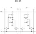
- FIG. 1A is a circuit diagram illustrating an individual sub pixel of an electroluminescent display device according to one embodiment of the present disclosure
- FIG. 1B is a circuit diagram illustrating an individual sub pixel of an electroluminescent display device according to another embodiment of the present disclosure.
- FIGs. 1A and 1B show only first and second sub pixels (P1, P2) disposed adjacent to each other.
- the first sub pixel (P1) may be any one among red, green, and blue sub pixels
- the second sub pixel (P2) may be another among the red, green, and blue sub pixels.
- each individual sub pixel (P1, P2) of the electroluminescent display device includes a gate line (GL), a high power source line (VDD), a data line (DL), and a reference line (Ref).
- GL gate line
- VDD high power source line
- DL data line
- Ref reference line
- the gate line (GL) and the high power source line (VDD) are arranged in a first direction, for example, a horizontal direction while being apart from each other.
- the data line (DL) and the reference line (Ref) are arranged in a second direction, for example, a vertical direction while being apart from each other, wherein the second direction is different from the first direction.
- Each of the first sub pixel (P1) and the second sub pixel (P2) are provided between one data line (DL) and another data line (DL).
- an interval between one data line (DL) and another data line (DL) defines a width of the first direction in the first sub pixel (P1) and the second sub pixel (P2).
- Each of the gate line (GL) and the high power source line (VDD) may be shared in the first sub pixel (P1) and the second sub pixel (P2).
- the gate line (GL), the high power source line (VDD), the data line (DL), and the reference line (Ref) constituting the individual sub pixel (P1, P2) according to the present disclosure are not limited to the structure of FIG. 1A .
- An arrangement structure of the gate line (GL), the high power source line (VDD), the data line (DL), and the reference line (Ref) may be changed in various ways generally known to those in the art.
- Each of the first sub pixel (P1) and the second sub pixel (P2) includes a switching thin film transistor (T1), a driving thin film transistor (T2), an initializing thin film transistor (T3), a capacitor (C1, C2), and a light emitting device such as an Organic Light-Emitting Diode (OLED).
- Each of the switching thin film transistor (T1), the driving thin film transistor (T2), and the initializing thin film transistor (T3) may be formed of an NMOS transistor.
- the switching thin film transistor (T1) which is switched by a gate signal supplied to the gate line (GL), supplies a data voltage, which is supplied from the data line (DL), to the driving thin film transistor (T2).
- the driving thin film transistor (T2) which is switched by the data voltage supplied from the switching thin film transistor (T1), generates a data current from a power source supplied from the high power source line (VDD), and then supplies the generated data current to the light emitting device (OLED).
- the initializing thin film transistor (T3) initializes a source voltage of the driving thin film transistor (T2), and removes charges from the light emitting device (OLED).
- the initializing thin film transistor (T3) supplies an initializing voltage, which is supplied from the reference line (Ref), to a source terminal of the driving thin film transistor (T2) in response to an initializing control signal supplied from the gate line (GL).
- the initializing control signal is supplied from the gate line (GL), but not limited to this structure.
- an initializing control line for supplying the initializing control signal to the initializing thin film transistor (T3) may be additionally provided.
- the initializing thin film transistor (T3) may supply a current based on a property value of the driving thin film transistor (T2) to the reference line (Ref).
- the capacitor (C1, C2) maintains the data voltage, which is supplied to the driving thin film transistor (T2), for one frame period.
- the capacitor (C1, C2) is connected with each of gate and source terminals of the driving thin film transistor (T2).
- the gate terminal of the driving thin film transistor (T2) is connected with a drain terminal of the switching thin film transistor (T1), and the source terminal of the driving thin film transistor (T2) is connected with an anode terminal of the light emitting device (OLED).
- the capacitor (C1, C2) may include a first capacitor (C1) provided in the first sub pixel (P1), and a second capacitor (C2) provided in the second sub pixel (P2).
- the first capacitor (C1) which extends from the first sub pixel (P1) to the second sub pixel (P2), is overlapped with the first sub pixel (P1) and the second sub pixel (P2)
- the second capacitor (C2) which extends from the second sub pixel (P2) to the first sub pixel (P1), is overlapped with the first sub pixel (P1) and the second sub pixel (P2) so that it is possible to increase a capacitance of the capacitor (C1, C2) without increasing the size of the sub pixel (P1, P2), which will be described in detail later.
- the light emitting device emits light in accordance with the data current supplied from the driving thin film transistor (T2).
- the light emitting device (OLED) may include an anode electrode connected with a source electrode of the driving thin film transistor (T2), and an organic emitting layer and a cathode electrode sequentially deposited on the anode electrode.
- the cathode electrode of the light emitting device (OLED) is connected with a low power source line (VSS).
- FIG. 1B is a circuit diagram illustrating an individual sub pixel of an electroluminescent display device according to another embodiment of the present disclosure, which is obtained by additionally providing a voltage holding line (VHL) in FIG. 1A .
- VHL voltage holding line
- the voltage holding line (VHL) supplies a voltage for constantly maintaining a voltage of the semiconductor substrate.
- the circuit diagram of FIG. 1B is not applied to a case of using a glass substrate or a plastic substrate.
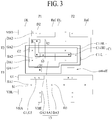
- FIGs. 2 to 4 are plane views illustrating an electroluminescent display device according to one embodiment of the present disclosure
- FIG. 2 illustrates remaining structures except the capacitor (C1, C2) in the circuit diagram of FIG. 1B
- FIG. 3 illustrates a structure obtained by additionally providing a first capacitor (C1) to FIG. 2
- FIG. 4 illustrates a structure obtained by additionally providing a second capacitor (C2) to FIG. 3 .
- the high power source line (VDD), the gate line (GL), and the voltage holding line (VHL) are arranged in a first direction, for example, a horizontal direction, and the data line (DL) and the reference line (Ref) are arranged in a second direction, for example, a vertical line.
- the high power source line (VDD) supplies power source to the driving thin film transistor (T2) of the individual sub pixel (P1, P2)
- the gate line (GL) supplies the gate signal to the switching thin film transistor (T1) of the individual sub pixel (P1, P2) and also supplies the initializing control signal to the initializing thin film transistor (T3) of the individual sub pixel (P1, P2)
- the data line (DL) supplies the data voltage to the switching thin film transistor (T1) of the individual sub pixel (P1, P2)
- the reference line (Ref) supplies the initializing voltage to the initializing thin film transistor (T3) of the individual sub pixel (P1, P2).
- the voltage holding line (VHL) supplies the voltage for constantly maintaining the voltage of the semiconductor substrate. If an insulating substrate such as glass or plastic is used for the electroluminescent display device according to the present disclosure, the voltage holding line (VHL) may be omitted.
- the switching thin film transistor (T1) the driving thin film transistor (T2), and the initializing thin film transistor (T3).
- the switching thin film transistor (T1) includes a first gate area (GA1), a first source area (SA1), and a first drain area (DA1).
- the first gate area (GA1) is connected with a first gate electrode (G1) through the via (x), and the first gate electrode (G1) is connected with the gate line (GL) through the via (x).
- the gate signal supplied to the gate line (GL) is supplied to the first gate area (GA1) via the first gate electrode (G1).
- the first gate electrode (G1) is patterned in the individual sub pixel (P1, P2) while being overlapped with the gate line (GL).
- the first gate area (GA1) may be consecutively extending from the first sub pixel (P1) to the second sub pixel (P2) while being overlapped with the first gate electrode (G1) and the gate line (GL).
- the first source area (SA1) may be connected with a first source electrode (S1) through the via (x), and the first source electrode (S1) may be diverged from the data line (DL).
- the data signal supplied to the data line (DL) may be supplied to the first source area (SA1) via the first source electrode (S1).
- the first source area (SA1) may be patterned in the individual sub pixel (P1, P2) while being overlapped with the first source electrode (S1).
- the first drain area (DA1) is connected with a first drain electrode (D1) through the via (x), and the first drain electrode (D1) is connected with the second gate electrode (G2) of the driving thin film transistor (T2).
- the data voltage which is switched by the switching thin film transistor (T1) is supplied to the second gate electrode (G2) via the first drain electrode (D1) in the first drain area (DA1).
- the first drain area (DA1) may be patterned in the individual sub pixel (P1, P2) while being overlapped with the first drain electrode (D1).
- the driving thin film transistor (T2) may include a second gate area (GA2), a second source area (SA2), and a second drain area (DA2).
- the second gate area (GA2) is connected with a second gate electrode (G2) through the via (x), and the second gate electrode (G2) is connected with the first drain electrode (D1).
- the data voltage of the first drain electrode (D1) is supplied as the gate signal of the second gate area (GA2) via the second gate electrode (G2).
- the second gate electrode (G2) may be formed as one body with the first drain electrode (D1), and the second gate area (GA2) may be patterned in the individual sub pixel (P1, P2) while being overlapped with the second gate electrode (G2).
- the second gate area (GA2) may extend to the data line (DL) of the neighboring sub pixel (P1, P2).
- the second source area (SA2) is connected with the second source electrode (S2) through the via (x), and the second source electrode (S2) is connected with the anode electrode through the via (x).
- the data current of the second source area (SA2) is supplied to the anode electrode via the second source electrode (S2).
- the second source area (SA2) and the second source electrode (S2) may be patterned in the individual sub pixel (P1, P2) while being overlapped with each other.
- the second drain area (DA2) is connected with the second drain electrode (D2) through the via (x), and the second drain electrode (D2) may be connected with the high power source line (VDD) through the via (x).
- the power source supplied from the high power source line (VDD) is supplied to the second drain area (DA2) via the second drain electrode (D2).
- the second drain area (DA2) is patterned in the individual sub pixel (P1, P2) while being overlapped with the second drain electrode (D2), and the second drain electrode (D2) may be patterned in the individual sub pixel (P1, P2) while being overlapped with the high power source line (VDD).
- the initializing thin film transistor (T3) includes a third gate area (GA3), a third source area (SA3), and a third drain area (DA3).
- the third gate area (GA3) is connected with a third gate electrode (G3) through the via (x), and the third gate electrode (G3) is connected with the gate line (GL) through the via (x).
- the initializing control signal supplied to the gate line (GL) is supplied to the third gate area (GA3) via the third gate electrode (G3).
- the third gate area (G3) is formed as one body with the first gate area (GA1), and the third gate electrode (G3) may be formed as one body with the first gate electrode (G1).
- the third gate electrode (G3) may be patterned in the individual sub pixel (P1, P2) while being overlapped with the gate line (GL), and the third gate area (GA3) may be consecutively extending from the first sub pixel (P1) to the second sub pixel (P2) while being overlapped with the third gate electrode (G3) and the gate line (GL).
- the third source area (SA3) is connected with the third source electrode (S3) through the via (x), and the third source electrode (S3) is connected with the second source electrode (S2).
- the data current of the second source electrode (S2) is supplied to the third source area (SA3) via the third source electrode (S3).
- the third source area (SA3) is formed as one body with the second source area (SA2), and the third source electrode (S3) may be formed as one body with the second source electrode (S2).
- the third source area (SA3) and the third source electrode (S3) may be patterned in the individual sub pixel (P1, P2) while being overlapped with each other.
- the third drain area (DA3) is connected with the third drain electrode (D3) through the via (x), and the third drain electrode (D3) is connected with the reference line (Ref).
- the voltage supplied from the reference line (Ref) may be supplied to the third drain area (DA3) via the third drain electrode (D3).
- the third drain area (DA3) may be patterned in the individual sub pixel (P1, P2) while being overlapped with the third drain electrode (D3), and the third drain electrode (D3) may be formed as one body with the reference line (Ref). That is, one portion of the reference line (Ref) may function as the third drain electrode (D3).
- a voltage holding area (VHA) is provided in the individual sub pixel (P1, P2), the voltage holding area (VHA) is connected with a voltage holding electrode (VHE) through the via (x), and the voltage holding electrode (VHE) is connected with the voltage holding line (VHL) through the via (x).
- VHA voltage holding area
- VHE voltage holding electrode
- VHL voltage holding line
- the voltage holding area (VHA) may be extending from the first sub pixel (P1) to the second sub pixel (P2) while being in parallel with the voltage holding line (VHL) and being spaced apart from the voltage holding line (VHL), or may be extending from the first sub pixel (P1) to the second sub pixel (P2) while being in parallel with the voltage holding line (VHL) and being overlapped with the voltage holding line (VHL), and the voltage holding electrode (VHE) may be patterned in the individual sub pixel (P1, P2).
- the first capacitor (C1) is provided in the first sub pixel (P1).
- the first capacitor (C1) includes a first capacitor lower electrode (C1-L) and a first capacitor upper electrode (C1-HL, C1-HH).
- the first capacitor lower electrode (C1-L) is connected with the second gate electrode (G2) of the first sub pixel (P1) through the via (x).
- the first capacitor lower electrode (C1-L) is extending from the first sub pixel (P1) to the second sub pixel (P2) while being overlapped with the first sub pixel (P1) and the second sub pixel (P2).
- the first capacitor lower electrode (C1-L), which extends from the first sub pixel (P1) to the second sub pixel (P2), is formed in a rectangular structure, however, a cut-off area is provided in the second sub pixel (P2).
- the first capacitor lower electrode (C1-L) is not formed in the cut-off area, wherein the cut-off area is the area wherein a second capacitor lower electrode (C2-L), which will be explained later, is connected with the second gate electrode (G2) of the second sub pixel (P2) through the via (x).
- the cut-off area is the area wherein a second capacitor lower electrode (C2-L), which will be explained later, is connected with the second gate electrode (G2) of the second sub pixel (P2) through the via (x).
- the first capacitor upper electrode (C1-HL, C1-HH) includes a first lower layer (C1-HL) and a first upper layer (C1-HH).
- the first lower layer (C1-HL) is connected with the first upper layer (CH-HH) through the via (x) provided in the first sub pixel (P1) and the second sub pixel (P2), and the first upper layer (C1-HH) may be connected with the second source electrode (S2) of the first sub pixel (P1) through the via (x) provided in the first sub pixel (P1).
- the first lower layer (C-HL) is connected with the second source electrode (S2) of the first sub pixel (P1) through the first upper layer (C1-HH).
- the first capacitor upper electrode (C1-HL, C1-HH) includes the first lower layer (C1-HL) and the first upper layer (C1-HH), whereby it is possible to increase a capacitance of the first capacitor (C1) by decreasing a distance between the first capacitor upper electrode (C1-HL, C1-HH) and the first capacitor lower electrode (C1-L), but not limited to this structure.
- the first capacitor upper electrode (C1-HL, C1-HH) may be formed of one electrode layer connected with the second source electrode (S2) of the first sub pixel (P1).
- the first lower layer (C1-HL) and the first upper layer (C1-HH) are extending from the first sub pixel (P1) to the second sub pixel (P2) while being overlapped with the first sub pixel (P1) and the second sub pixel (P2).
- the first upper layer (C1-HH) may be not extending to the second sub pixel (P2).
- An area of the first lower layer (C1-HL) is relatively larger than an area of the first upper layer (C1-HH) so that it is possible to increase a capacitance of the first capacitor (C1).
- the area of the first lower layer (C1-HL) is relatively smaller than an area of the first capacitor lower electrode (C1-L), but not limited to this structure.
- the first capacitor upper electrode (C1-HL, C1-HH) is connected with the second gate electrode (G2) of the first sub pixel (P1) through the via (x), and the first capacitor lower electrode (C1-L) may be connected with the second source electrode (S2) of the first sub pixel (P1) through the via (x).
- the second capacitor (C2) is provided in the second sub pixel (P2).
- the second capacitor (C2) is overlapped with the first capacitor (C1).
- the second capacitor (C2) and the first capacitor (C1) may be provided in the different layers from each other.
- the second capacitor (C2) includes a second capacitor lower electrode (C2-L) and a second capacitor upper electrode (C2-HL, C2-HH).
- the second capacitor lower electrode (C2-L) is connected with the second gate electrode (G2) of the second sub pixel (P2) through the via (x) in the cut-off area of the first capacitor lower electrode (C1-L).
- the second capacitor lower electrode (C2-L) is extending from the second sub pixel (P2) to the first sub pixel (P1) while being overlapped with the first sub pixel (P1) and the second sub pixel (P2).
- the second capacitor lower electrode (C2-L) which extends from the second sub pixel (P2) to the first sub pixel (P1), is formed in a rectangular structure, and a cut-off area is not provided in the second capacitor lower electrode (C2-L) unlike the first capacitor lower electrode (C1-L).
- an area of the second capacitor lower electrode (C2-L) may be relatively larger than an area of the first capacitor lower electrode (C1-L), but not limited to this structure.
- the second capacitor lower electrode (C2-L) may be overlapped with the first capacitor lower electrode (C1-L) and the first capacitor upper electrode (C1-HL, C1-HH) constituting the first capacitor (C1).
- the second capacitor upper electrode (C2-HL, C2-HH) includes a second lower layer (C2-HL) and a second upper layer (C2-HH).
- the second lower layer (C2-HL) is connected with the second upper layer (C2-HH) through the via (x) provided in the first sub pixel (P1) and the second sub pixel (P2), and the second upper layer (C2-HH) may be connected with the second source electrode (S2) of the second sub pixel (P2) through the via (x) provided in the second sub pixel (P2).
- the second lower layer (C2-HL) is connected with the second source electrode (S2) of the second sub pixel (P2) through the second upper layer (C2-HH).
- the second capacitor upper electrode (C2-HL, C2-HH) includes the second lower layer (C2-HL) and the second upper layer (C2-HH) so that it is possible to increase a capacitance of the second capacitor (C2) by decreasing a distance between the second capacitor upper electrode (C2-HL, C2-HH) and the second capacitor lower electrode (C2-L), but not limited to this structure.
- the second capacitor upper electrode (C2-HL, C2-HH) may be formed as one electrode layer connected with the second source electrode (S2) of the second sub pixel (P2).
- the second lower layer (C2-HL) and the second upper layer (C2-HH) are extending from the second sub pixel (P2) to the first sub pixel (P1) while being overlapped with the first sub pixel (P1) and the second sub pixel (P2).
- the second upper layer (C2-HH) may be not extending to the first sub pixel (P1).
- An area of the second lower layer (C2-HL) is relatively larger than an area of the second upper layer (C2-HH) so that it is possible to increase a capacitance of the second capacitor (C2).
- the area of the second lower layer (C2-HL) may be relatively smaller than an area of the second capacitor lower electrode (C2-L), but not limited to this structure.
- the second lower layer (C2-HL) may be overlapped with the first capacitor lower electrode (C1-L) and the first capacitor upper electrode (C1-HL, C1-HH) constituting the first capacitor (C1).
- the second upper layer (C2-HH) is overlapped with the first lower layer (C1-HL) and the first capacitor lower electrode (C1-L) of the first capacitor (C1), but not overlapped with the first upper layer (C1-HH).
- the second upper layer (C2-HH) may be overlapped with the first upper layer (C1-HH).
- the second capacitor upper electrode (C2-HL, C2-HH) is connected with the second gate electrode (G2) of the second sub pixel (P2) through the via (x), and the second capacitor lower electrode (C2-L) may be connected with the second source electrode (S2) of the second sub pixel (P2) through the via (x).
- FIG. 5 is a cross sectional view illustrating the first sub pixel (P1) and the second sub pixel (P2) of the electroluminescent display device according to one embodiment of the present disclosure, which shows an electrical connection between the driving thin film transistor (T2) and the capacitor electrode (C1, C2) shown in FIGs. 2 to 4 .
- the second source area (SA2) and the second drain area (DA2) are provided in the substrate 100.
- the second source area (SA1) and the second drain area (DA2) are provided in each of the first sub pixel (P1) and the second sub pixel (P2).
- the substrate 100 may be formed of a P-type semiconductor, and the second source area (SA2) and the second drain area (DA2) may be formed of N-type doping areas obtained by doping predetermined areas of the substrate 100 with N-type dopant.
- a gate insulating layer 300 is formed on the substrate 100, and the second gate area (GA2) is formed on the gate insulating layer 300.
- the gate insulating layer 300 and the second gate area (GA2) are formed in each of the first sub pixel (P1) and the second sub pixel (P2).
- the second gate area (GA2) may be formed of poly silicon, but not limited to this material.
- a first insulating layer 210 is formed on the second gate area (GA2), and the second source electrode (S2), the second gate electrode (G2), and the second drain electrode (D2) are formed on the first insulating layer 210.
- the second source electrode (S2), the second gate electrode (G2), and the second drain electrode (D2) are formed in each of the first sub pixel (P1) and the second sub pixel (P2).
- the second source electrode (S2) is connected with the second source area (SA2) through the via penetrating through the first insulating layer 210
- the second gate electrode (G2) is connected with the second gate area (GA2) through the via penetrating through the first insulating layer 210
- the second drain electrode (D2) is connected with the second drain area (DA2) through the via penetrating through the first insulating layer 210.
- a second insulating layer 220 is formed on the second source electrode (S2), the second gate electrode (G2), and the second drain electrode (D2). Then, a first connection electrode (CE1), a second connection electrode (CE2), a third connection electrode (CE3), and the first capacitor lower electrode (C1-L) are formed on the second insulating layer 220.
- the first connection electrode (CE1) and the second connection electrode (CE2) are formed in the second sub pixel (P2)
- the third connection electrode (CE3) is formed in the first sub pixel (P1)
- the first capacitor lower electrode (C1-L) extends from the first sub pixel (P1) to the second sub pixel (P2).
- the first connection electrode (CE1) is connected with the second source electrode (S2) of the second sub pixel (P2) through the via penetrating through the second insulating layer 220
- the second connection electrode (CE2) is connected with the second gate electrode (G2) of the second sub pixel (P2) through the via penetrating through the second insulating layer 220
- the third connection electrode (CE3) is connected with the second source electrode (S2) of the first sub pixel (P1) through the via penetrating through the second insulating layer 220
- the first capacitor lower electrode (C1-L) is connected with the second gate electrode (G2) of the first sub pixel (P1) through the via penetrating through the second insulating layer 220.
- a first insulating interlayer 410 is formed on the first capacitor lower electrode (C1-L), and the lower layer (C1-HL) of the first capacitor upper electrode (C1-HL, C1-HH) is formed on the first insulating interlayer 410.
- the first insulating interlayer 410 and the lower layer (C1-HL) of the first capacitor upper electrode (C1-HL, C1-HH) extend from the first sub pixel (P1) to the second sub pixel (P2).
- a third insulating layer 230 is formed on the lower layer (C1-HL) of the first capacitor upper electrode (C1-HL, C1-HH). Then, a fourth connection electrode (CE4), a fifth connection electrode (CE5), and the upper layer (C1-HH) of the first capacitor upper electrode (C1-HL, C1-HH) are formed on the third insulating layer 230.
- the fourth connection electrode (CE4) and the fifth connection electrode (CE5) are formed in the second sub pixel (P2), and the upper layer (C1-HH) of the first capacitor upper electrode (C1-HL, C1-HH) extends from the first sub pixel (P1) to the second sub pixel (P2).
- the fourth connection electrode (CE4) is connected with the first connection electrode (CE1) of the second sub pixel (P2) through the via penetrating through the third insulating layer 230
- the fifth connection electrode (CE5) is connected with the second connection electrode (CE2) of the second sub pixel (P2) through the via penetrating through the third insulating layer 230.
- the upper layer (C1-HH) of the first capacitor upper electrode (C1-HL, C1-HH) is connected with the lower layer (C1-HL) of the first capacitor upper electrode (C1-HL, C1-HH) through the via penetrating through the third insulating layer 230.
- the capacitance is generated between the first capacitor lower electrode (C1-L) and the lower layer (C1-HL) of the first capacitor upper electrode (C1-HL, C1-HH) which are spaced apart from each other with the first insulating interlayer 410 with a small thickness interposed in-between.
- a distance between the first capacitor lower electrode (C1-L) and the lower layer (C1-HL) of the first capacitor upper electrode (C1-HL, C1-HH), that is, the thickness of the first insulating interlayer 410 is shorter than a distance between the lower layer (C1-HL) of the first capacitor upper electrode (C1-HL, C1-HH) and the upper layer (C1-HH) of the first capacitor upper electrode (C1-HL, C1-HH), to thereby increase the capacitance.
- the capacitance may be generated between the first capacitor lower electrode (C1-L) and the upper layer (C1-HH) which are spaced apart from each other with the third insulating layer 230 interposed in-between.
- a fourth insulating layer 240 is formed on the fourth connection electrode (CE4), the fifth connection electrode (CE5), and the upper layer (C1-HH). Then, a sixth connection electrode (CE6), a seventh connection electrode (CE7), and the second capacitor lower electrode (C2-L) are formed on the fourth insulating layer 240.
- the sixth connection electrode (CE6) is formed in the second sub pixel (P2)
- the seventh connection electrode (CE7) is formed in the first sub pixel (P1)
- the second capacitor lower electrode (C2-L) extends from the second sub pixel (P2) to the first sub pixel (P1).
- the sixth connection electrode (CE6) is connected with the fourth connection electrode (CE4) through the via penetrating through the fourth insulating layer 240
- the seventh connection electrode (CE7) is connected with the upper layer (C1-HH) of the first capacitor upper electrode (C1-HL, C1-HH) through the via penetrating through the fourth insulating layer 240
- the second capacitor lower electrode (C2-L) is connected with the fifth connection electrode (CE5) through the via penetrating through the fourth insulating layer 240.
- the second capacitor lower electrode (C2-L) is connected with the second gate electrode (G2) of the second sub pixel (P2) via the fifth connection electrode (CE5) and the second connection electrode (CE2).
- a second insulating interlayer 420 is formed on the second capacitor lower electrode (C2-L), and the lower layer (C2-HL) of the second capacitor upper electrode (C2-HL, C2-HH) is formed on the second insulating interlayer 420.
- the second insulating interlayer 420 and the lower layer (C2-HL) of the second capacitor upper electrode (C2-HL, C2-HH) extend from the second sub pixel (P2) to the first sub pixel (P1).
- a fifth insulating layer 250 is formed on the lower layer (C2-HL) of the second capacitor upper electrode (C2-HL, C2-HH). Then, an eighth connection electrode (CE8), and the upper layer (C2-HH) of the second capacitor upper electrode (C2-HL, C2-HH) are formed on the fifth insulating layer 250.
- the eighth connection electrode (CE8) is formed in the first sub pixel (P1), and the upper layer (C2-HH) of the second capacitor upper electrode (C2-HL, C2-HH) extend from the second sub pixel (P2) to the first sub pixel (P1).
- the eighth connection electrode (CE8) is connected with the seventh connection electrode (CE7) through the via penetrating through the fifth insulating layer 250, and the upper layer (C2-HH) of the second capacitor upper electrode (C2-HL, C2-HH) is connected with the lower layer (C2-HL) of the second capacitor upper electrode (C2-HL, C2-HH) through the via penetrating through the fifth insulating layer 250.
- the capacitance is generated between the second capacitor lower electrode (C2-L) and the lower layer (C2-HL) of the second capacitor upper electrode (C2-HL, C2-HH) which are spaced apart from each other with the second insulating interlayer 420 with a small thickness interposed in-between.
- a distance between the second capacitor lower electrode (C2-L) and the lower layer (C2-HL) of the second capacitor upper electrode (C2-HL, C2-HH), that is, the thickness of the second insulating interlayer 420 is shorter than a distance between the lower layer (C2-HL) of the second capacitor upper electrode (C2-HL, C2-HH) and the upper layer (C2-HH) of the second capacitor upper electrode (C2-HL, C2-HH), to thereby increase the capacitance.
- the capacitance may be generated between the second capacitor lower electrode (C2-L) and the upper layer (C2-HH) which are spaced apart from each other with the fifth insulating layer 250 interposed in-between.
- a sixth insulating layer 260 is formed on the eighth connection electrode (CE8) and the second capacitor upper electrode (C2-HL, C2-HH), and a first electrode 500, which functions as an anode, is formed on the sixth insulating layer 260.
- the first electrode 500 is formed in each of the first sub pixel (P1) and the second sub pixel (P2).
- the first electrode 500 of the first sub pixel (P1) is connected with the eighth connection electrode (CE8) through the via penetrating through the sixth insulating layer 260.
- the first electrode 500 of the first sub pixel (P1) is connected with the upper layer (C1-HH) of the first capacitor upper electrode (C1-HL, C1-HH) via the eighth connection electrode (CE8) and the seventh connection electrode (CE7).
- the first electrode 500 of the second sub pixel (P2) is connected with the upper layer (C2-HH) of the second capacitor upper electrode (C2-HL, C2-HH) through the via penetrating through the sixth insulating layer 260.
- Both ends of the first electrode 500 are covered by a bank 550.
- the bank 550 is provided to cover both ends of the first electrode 500 on the sixth insulating layer 260, and is also provided in the boundary area between the first sub pixel (P1) and the second sub pixel (P2).
- an exposed area of the first electrode 500 which is exposed without being covered by the bank 550, becomes an emission area.
- An emission layer 600 is formed on the first electrode 500.
- the emission layer 600 may be formed on the bank 550. That is, the emission layer 600 may be formed in each of the first sub pixel (P1) and the second sub pixel (P2), and the boundary area between the first sub pixel (P1) and the second sub pixel (P2).
- the emission layer 600 may be provided to emit white colored light (W). To this end, the emission layer 600 may include a plurality of stacks configured to emit different colored light.
- the emission layer 600 may include a first stack 610 configured to emit blue colored light, a second stack 630 configured to emit yellow colored light, and a charge generation layer (CGL) 620 provided between the first stack 610 and the second stack 630.
- Each of the first stack 610 and the second stack 630 may be formed in a deposition structure obtained by sequentially depositing a hole transporting layer, an organic emitting layer, and an electron transporting layer.
- the emission layer 600 may include a first stack configured to emit blue colored light, a second stack configured to emit green colored light, a third stack configured to emit red colored light, a first charge generation layer provided between the first stack and the second stack, and a second charge generation layer provided between the second stack and the third stack.
- a structure of the emission layer 600 may be changed in various ways generally known to those in the art.
- the emission layer 600 may be provided to emit different colored light by each individual sub pixel (P1, P2).
- a trench (T) may be provided in the bank 550 and the sixth insulating layer 260, whereby the emission layer 600 may be provided in the trench (T).
- the trench (T) may be formed only in the bank 500.
- the trench (T) is formed in the boundary between the sub pixels (P1, P2), and the emission layer 600 is formed in the trench (T) so that it is possible to reduce a leakage current between the neighboring sub pixels (P1, P2).
- the first stack 610 may be formed on an inner lateral surface of the trench (T), and may be formed on an inner lower surface of the trench (T). In this case, some area of the first stack 610 formed on the inner lateral surface of the trench (T) is disconnected from some area of the first stack 610 formed on the inner lower surface of the trench (T). Thus, some area of the first stack 610 formed on one lateral surface inside the trench (T), and more particularly, on the left lateral surface inside the trench (T) is not connected with some area of the first stack 610 formed on the other lateral surface inside the trench (T), and more particularly, on the right lateral surface inside the trench (T). Accordingly, charges are not transferred between the neighboring sub pixels (P1, P2) arranged with the trench (T) interposed in-between through the first stack 610.
- the charge generating layer 620 may be formed at the inner lateral surface of the trench (T) while being disposed on the first stack 610.
- some area of the charge generating layer 620 formed on one lateral surface inside the trench (T), and more particularly, on the left lateral surface inside the trench (T) is not connected with some area of the charge generating layer 620 formed on the other lateral surface inside the trench (T), and more particularly, on the right lateral surface inside the trench (T). Accordingly, charges are not transferred between the sub pixels (P1, P2) arranged with the trench (T) interposed in-between through the charge generating layer 620.
- the second stack 630 may be provided connectedly between the neighboring sub pixels (P1, P2) with the trench (T) interposed in-between while being disposed on the charge generating layer 620.
- charges may be transferred between the sub pixels (P1, P2) with the trench (T) interposed in-between through the second stack 630, but not limited to this structure.
- the second stack 630 may be provided disconnectedly between the neighboring sub pixels (P1, P2) with the trench (T) interposed in-between by appropriately adjusting a shape of the trench (T) and a deposition process of the emission layer 600.
- some lower portions of the second stack 630 being adjacent to the charge generation layer 620 may be disconnectedly provided between the sub pixels (P1, P2).
- Conductivity of the charge generating layer 620 is higher than that of each of the first stack 610 and the second stack 630.
- an N-type charge generating layer of the charge generating layer 620 may comprise a metal material, whereby conductivity of the charge generating layer 620 is higher than that of each of the first stack 610 and the second stack 630.
- the charge transfer between the sub pixels (P1, P2) which are adjacent to each other is generally made through the charge generating layer 620, and the charge transfer through the second stack 630 is insignificant.
- the emission layer 600 when the emission layer 600 is formed inside the trench (T), some of the emission layer 600 is disconnectedly provided. Especially, the first stack 610 and the charge generating layer 620 are provided disconnectedly so that it is possible to reduce the charge transfer between the neighboring sub pixels (P1, P2), to thereby prevent a leakage current.
- a second electrode 700 which functions as a cathode, is formed on the emission layer 600.
- the second electrode 700 is formed in each of the sub pixels (P1, P2), and also formed in the boundary between the sub pixels (P1, P2). That is, the second electrode 700 may be formed above the bank 550.
- An encapsulation layer 800 is formed on the second electrode 700, to thereby prevent external moisture from being permeated into the emission layer 600.
- the encapsulation layer 800 may be formed in a single-layered structure of an inorganic insulating material, or a deposition structure obtained by alternately depositing an inorganic insulating material and an organic insulating material, but not limited to these structures.
- a color filter layer 900 is formed on the encapsulation layer 800.
- the color filter layer 900 confronts the emission area inside the individual sub pixel (P1, P2).
- the color filter layer 900 may include a red (R) color filter, a green (G) color filter, and a blue color filter, but not limited to this structure.
- a black matrix may be additionally provided in the boundary between each of color filters in the color filter layer 900, to thereby prevent light from leaking into the remaining areas except the emission area.
- FIG. 6 is a cross sectional view illustrating the electroluminescent display device according to one embodiment of the present disclosure, which shows a deposition structure of the thin film transistor (T1, T2, T3), the gate line (GL), the data line (DL), the high power source line (VDD1, VDD2), the reference line (Ref), and the voltage holding line (VHL) shown in FIGs. 2 to 4 .
- structures provided above the fifth insulating layer 250 for example, the anode electrode, the emission layer, and the cathode electrode are not shown, and the electrical connection structure between the anode electrode and the second source electrode (S2) of the driving thin film transistor (T2) described in FIG. 5 is also not shown.
- a switching thin film transistor (T1) area As shown in FIG. 6 , a switching thin film transistor (T1) area, a driving thin film transistor (T2) area, a initializing thin film transistor (T3) area, and a voltage holding structure (VHS) area are formed on the substrate 100.
- T1 area a switching thin film transistor (T1) area, a driving thin film transistor (T2) area, a initializing thin film transistor (T3) area, and a voltage holding structure (VHS) area are formed on the substrate 100.
- VHS voltage holding structure
- the first source area (SA1) and the first drain area (DA1) are formed in the switching thin film transistor (T1) area of the substrate 100
- the second source area (SA2) and the second drain area (DA2) are formed in the driving thin film transistor (T2) area of the substrate 100
- the third source area (SA3) and the third drain area (DA3) are formed in the initializing thin film transistor (T3) area of the substrate 100
- the voltage holding area (VHA) is formed in the voltage holding structure (VHS) area of the substrate 100.
- the substrate 100 is formed of a P-type semiconductor.
- Each of the first source area (SA1), the first drain area (DA1), the second source area (SA2), the second drain area (DA2), the third source area (SA3), and the third drain area (DA3) is formed of an N-type doping area obtained by doping a predetermined area of the substrate 100 with N-type dopant.
- the voltage holding area (VHA) may be formed of a P+-type doping area obtained by doping a predetermined area of the substrate 100 with P-type dopant.
- the gate insulating layer 300 and the first gate area (GA1), which are provided in the same pattern, are sequentially formed on the substrate 100 between the first source area (SA1) and the first drain area (DA1).
- the gate insulating layer 300 and the second gate area (GA2), which are provided in the same pattern, are sequentially formed on the substrate 100 between the second source area (SA2) and the second drain area (DA2).
- the gate insulating layer 300 and the third gate area (GA3), which are provided in the same pattern, are sequentially formed on the substrate 100 between the third source area (SA3) and the third drain area (DA3).
- the first gate area (GA1), the second gate area (GA2), and the third gate area (GA3) may be provided in the same layer, and may be formed of the same material.
- the first insulating layer 210 is formed on the first gate area (GA1), the second gate area (GA2), and the third gate area (GA3).
- the first source electrode (S1), the first gate electrode (G1), and the first drain electrode (D1) are formed in the switching thin film transistor (T1) area on the first insulating layer 210.
- the second source electrode (S2), the second gate electrode (G2), and the second drain electrode (D2) are formed in the driving thin film transistor (T2) area on the first insulating layer 210.
- the third source electrode (S3), the third gate electrode (G3), and the third drain electrode (D3) are formed in the initializing thin film transistor (T3) area on the first insulating layer 210.
- the voltage holding electrode (VHE) is formed in the voltage holding structure (VHS) area on the first insulating layer 210.
- the first source electrode (S1) is connected with the first source area (SA1) through the via penetrating through the first insulating layer 210
- the first gate electrode (G1) is connected with the first gate area (GA1) through the via penetrating through the first insulating layer 210
- the first drain electrode (D1) is connected with the first drain area (DA1) through the via penetrating through the first insulating layer 210.
- the second source electrode (S2) is connected with the second source area (SA2) through the via penetrating through the first insulating layer 210
- the second gate electrode (G2) is connected with the second gate area (GA2) through the via penetrating through the first insulating layer 210
- the second drain electrode (D2) is connected with the second drain area (DA2) through the via penetrating through the first insulating layer 210.
- the voltage holding electrode (VHE) is connected with the voltage holding area (VHA) through the via penetrating through the first insulating layer 210.
- the first source electrode (S1), the first gate electrode (G1), the first drain electrode (D1), the second source electrode (S2), the second gate electrode (G2), the second drain electrode (D2), the third source electrode (S3), the third gate electrode (G3), the third drain electrode (D3), and the voltage holding electrode (VHE) may be provided in the same layer, and may be formed of the same material.
- the first source electrode (S1) of the switching thin film transistor (T1) area is connected with the data line (DL), and more particularly, is formed as one body with the data line (DL).
- the data line (DL) is provided in the same layer as that of the first source electrode (S1), and is formed of the same material as that of the first source electrode (S1).
- the third drain electrode (D3) of the initializing thin film transistor (T3) area is connected with the reference line (Ref), and is formed as one body with the reference line (Ref).
- the reference line (Ref) is provided in the same layer as that of the third drain electrode (D3), and is formed of the same material as that of the third drain electrode (D3).
- the second gate electrode (G2) is connected with the first drain electrode (D1), and the second source electrode (S2) is connected with the third source electrode (S3). Also, the first gate electrode (G1) may be connected with the third gate electrode (G3).
- the second insulating layer 220 is formed on the first source electrode (S1), the first gate electrode (G1), the first drain electrode (D1), the second source electrode (S2), the second gate electrode (G2), the second drain electrode (D2), the third source electrode (S3), the third gate electrode (G3), the third drain electrode (D3), and the voltage holding electrode (VHE).
- the gate line (GL), the first high power source line (VDD1), and the voltage holding line (VHL) are formed on the second insulating layer 220.
- the gate line (GL) may be shared in the switching thin film transistor (T1) and the initializing thin film transistor (T3). Thus, the gate line (GL) may be connected with each of the first gate electrode (G1) and the third gate electrode (G3) through the via penetrating through the second insulating layer 220.
- the first high power source line (VDD1) is connected with the second drain electrode (D2) through the via penetrating through the second insulating layer 220, and the voltage holding line (VHL) is connected with the voltage holding electrode (VHE) through the via penetrating through the second insulating layer 220.
- the gate line (GL), the first high power source line (VDD1), and the voltage holding line (VHL) are provided in the same layer, and are formed of the same material.
- the third insulating layer 230 is formed on the gate line (GL), the first high power source line (VDD1), and the voltage holding line (VHL), and a ninth connection electrode (CE9) is formed on the third insulating layer 230.
- the ninth connection electrode (CE9) is connected with the first high power source line (VDD1) through the via penetrating through the third insulating layer 230.
- the fourth insulating layer 240 is formed on the ninth connection electrode (CE9), and a tenth connection electrode (CE10) is formed on the fourth insulating layer 240.
- the tenth connection electrode (CE10) is connected with the ninth connection electrode (CE9) through the via penetrating through the fourth insulating layer 240.
- the fifth insulating layer 250 is formed on the tenth connection electrode (CE10), and the second high power source line (VDD2) is formed on the fifth insulating layer 250.
- the second high power source line (VDD2) is connected with the tenth connection electrode (CE10) through the via penetrating through the fifth insulating layer 250.
- the second high power source line (VDD2) is connected with the first high power source line (VDD1) via the tenth connection electrode (CE10) and the ninth connection electrode (CE9).
- the high power source line (VDD1, VDD2) includes the first high power source line (VDD1) and the second high power source line (VDD2) which are provided in the different layers and are electrically connected with each other, whereby it is possible to stably supply the high power source to the second drain electrode (D2) of the driving thin film transistor (T2).
- the first high power source line (VDD1) and the second high power source line (VDD2) are provided in a continuous straight-line shape along a horizontal direction, but not limited to this structure.
- the second high power source line (VDD2) may be provided in a continuous straight-line shape along a horizontal direction
- the first high power source line (VDD1) may be provided in a discontinuous straight-line shape along the horizontal direction.
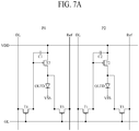
- FIG. 7A is a circuit diagram of an individual sub pixel (P1, P2) of an electroluminescent display device according to another embodiment of the present disclosure
- FIG. 7B is a circuit diagram of an individual sub pixel of an electroluminescent display device according to another embodiment of the present disclosure.
- the electroluminescent display device of FIG. 7A is identical to the electroluminescent display device of FIG. 1A , whereby only the different structures will be described in detail.
- the switching thin film transistor (T1), the driving thin film transistor (T2), and the initializing thin film transistor (T3) are formed of NMOS transistors.
- a switching thin film transistor (T1), a driving thin film transistor (T2), and a initializing thin film transistor (T3) are formed of PMOS transistors.
- each of the first capacitor (C1) provided in the first sub pixel (P1) and the second capacitor (C2) provided in the second sub pixel (P2) is connected with the gate and source terminals of the driving thin film transistor (T2), wherein the gate terminal of the driving thin film transistor (T2) is connected with the drain terminal of the switching thin film transistor (T1), and the source terminal of the driving thin film transistor (T2) is connected with the anode terminal of the light emitting device (OLED).
- each of a first capacitor (C1) provided in a first sub pixel (P1) and a second capacitor (C2) provided in a second sub pixel (P2) is connected with gate and source terminals of the driving thin film transistor (T2), wherein the gate terminal of the driving thin film transistor (T2) is connected with a drain terminal of the switching thin film transistor (T1), and the source terminal of the driving thin film transistor (T2) is connected with a high power source line (VDD).
- VDD high power source line
- FIG. 7B shows that a voltage holding line (VHL) is additionally provided. If the electroluminescent display device according to the present disclosure uses a semiconductor substrate such as silicon wafer, the voltage holding line (VHL) supplies a voltage for constantly maintaining a voltage of the semiconductor substrate. Thus, the circuit diagram of FIG. 7B is not applied to a case of using a glass substrate or a plastic substrate.
- VHL voltage holding line
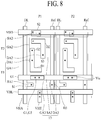
- FIGs. 8 to 10 are plane views illustrating the electroluminescent display device according to another embodiment of the present disclosure.
- FIG. 8 illustrates remaining structures except the capacitor (C1, C2) in the circuit diagram of FIG. 7B
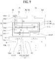
- FIG. 9 illustrates a structure obtained by additionally providing the first capacitor (C1) to FIG. 8
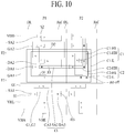
- FIG. 10 illustrates a structure obtained by additionally providing the second capacitor (C2) to FIG. 9 .
- the electroluminescent display device of FIG. 8 is identical in structure to the electroluminescent display device of FIG. 2 .
- T2 driving thin film transistor
- the driving thin film transistor (T2) of the individual sub pixel (P1, P2) includes a second gate area (GA2), a second source area (SA2), and a second drain area (DA2).
- the second source area (SA2) is connected with a second source electrode (S2) through the via (x), and the second source electrode (S2) is connected with the high power source line (VDD) through the via (x).
- the second source area (SA2) may be patterned in the individual sub pixel (P1, P2) while being overlapped with the second source electrode (S2), and the second source electrode (S2) may be patterned in the individual sub pixel (P1, P2) while being overlapped with the high power source line (VDD).
- the second drain area (DA2) is connected with a second drain electrode (D2) through the via (x), and the second drain electrode (D2) is connected with an anode electrode (not shown) through the via (x).
- the second drain area (DA2) and the second drain electrode (D2) may be patterned in the individual sub pixel (P1, P2) while being overlapped with each other.
- the second drain area (DA2) is connected with a second source area (SA2) of the initializing thin film transistor (T3), and the second drain electrode (D2) is connected with a second source electrode (S2) of the initializing thin film transistor (T3).
- the second drain area (DA2) is formed as one body with the second source area (SA2), and the second drain electrode (D2) is formed as one body with the second source electrode (S2).
- the first capacitor (C1) is provided in the first sub pixel (P1).
- the first capacitor (C1) includes a first capacitor lower electrode (C1-L) and a first capacitor upper electrode (C1-HL, C1-HH).
- the first capacitor lower electrode (C1-L) is connected with a second gate electrode (G2) of the first sub pixel (P1) through the via (x). Especially, the first capacitor lower electrode (C1-L), which extends from the first sub pixel (P1) to the second sub pixel (P2), is overlapped with the first sub pixel (P1) and the second sub pixel (P2), and a cut-off area is provided in the second sub pixel (P2).
- the first capacitor upper electrode (C1-HL, C1-HH) includes a first lower layer (C1-HL) and a first upper layer (C1-HH).
- the first lower layer (C1-HL) is connected with the first upper layer (C1-HH) through the via (x) provided in the first sub pixel (P1) and the second sub pixel (P2), and the first upper layer (C1-HH) is connected with the high power source line (VDD) through the via (x) provided in the first sub pixel (P1).
- the first lower layer (C1-HL) is connected with the high power source line (VDD) through the first upper layer (C1-HH).
- the first lower layer (C1-HL) and the first upper layer (C1-HH) are extending from the first sub pixel (P1) to the second sub pixel (P2), and are overlapped with the first sub pixel (P1) and the second sub pixel (P2).
- the first upper layer (C1-HH) may be not extending to the second sub pixel (P2).
- An area of the first lower layer (C1-HL) is relatively larger than an area of the first upper layer (C1-HH) so that it is possible to increase a capacitance of the first capacitor (C1). Meanwhile, the area of the first lower layer (C1-HL) is relatively smaller than an area of the first capacitor lower electrode (C1-L), but not limited to this structure.
- the second capacitor (C2) is provided in the second sub pixel (P2).
- the second capacitor (C2) is overlapped with the first capacitor (C1).
- the second capacitor (C2) includes a second capacitor lower electrode (C2-L) and a second capacitor upper electrode (C2-HL, C2-HH).
- the second capacitor lower electrode (C2-L) is connected with the second gate electrode (G2) of the second sub pixel (P2) through the via (x) in the cut-off area of the first capacitor lower electrode (C1-L).
- the second capacitor lower electrode (C2-L) which extends from the second sub pixel (P2) to the first sub pixel (P1), is overlapped with the first sub pixel (P1) and the second sub pixel (P2).
- the second capacitor lower electrode (C2-L) is not provided with the additional cut-off area.
- an area of the second capacitor lower electrode (C2-L) is larger than an area of the first capacitor lower electrode (C1-L).
- the second capacitor lower electrode (C2-L) may be overlapped with the first capacitor lower electrode (C1-L) and the first capacitor upper electrode (C1-HL, C1-HH) constituting the first capacitor (C1).
- the second capacitor upper electrode (C2-HL, C2-HH) includes a second lower layer (C2-HL) and a second upper layer (C2-HH).
- the second lower layer (C2-HL) may be connected with the second upper layer (C2-HH) through the via provided in the first sub pixel (P1) and the second sub pixel (P2), and the second upper layer (C2-HH) may be connected with the high power source line (VDD).
- the second lower layer (C2-HL) is connected with the high power source line (VDD) through the second upper layer (C2-HH).
- the second upper layer (C2-HH) may be diverged from the high power source line (VDD), whereby the second upper layer (C2-HH) may be formed as one body with the high power source line (VDD).
- the second upper layer (C2-HH) may be not extending to the first sub pixel (P1).
- An area of the second lower layer (C2-HL) is relatively larger than an area of the second upper layer (C2-HH) so that it is possible to increase a capacitance of the second capacitor (C2).
- the area of the second lower layer (C2-HL) may be relatively smaller than an area of the second capacitor lower electrode (C2-L), but not limited to this structure.
- the second lower layer (C2-HL) may be overlapped with the first capacitor lower electrode (C1-L) and the first capacitor upper electrode (C1-HL, C1-HH) constituting the first capacitor (C1).
- the second upper layer (C2-HH) is overlapped with the first lower layer (C1-HL) and the first capacitor lower electrode (C1-L) of the first capacitor (C1), but not overlapped with the first upper layer (C1-HH).
- the second upper layer (C2-HH) may be overlapped with the first upper layer (C1-HH).
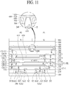
- FIG. 11 is a cross sectional view illustrating the first sub pixel (P1) and the second sub pixel (P2) of the electroluminescent display device according to another embodiment of the present disclosure, which shows an electrical connection between the driving thin film transistor (T2) and the capacitor electrode (C1, C2) shown in FIGs. 8 to 10 .
- T2 driving thin film transistor
- C1, C2 capacitor electrode
- the second source area (SA2) and the second drain area (DA2) are provided in the substrate 100.
- a gate insulating layer 300 is formed on the substrate 100, and the second gate area (GA2) is formed on the gate insulating layer 300.
- a first insulating layer 210 is formed on the second gate area (GA2), and the second source electrode (S2), the second gate electrode (G2), and the second drain electrode (D2) are formed on the first insulating layer 210.
- the second source electrode (S2) is connected with the second source area (SA2) through the via penetrating through the first insulating layer 210
- the second gate electrode (G2) is connected with the second gate area (GA2) through the via penetrating through the first insulating layer 210
- the second drain electrode (D2) is connected with the second drain area (DA2) through the via penetrating through the first insulating layer 210.
- a second insulating layer 220 is formed on the second source electrode (S2), the second gate electrode (G2), and the second drain electrode (D2). Then, an eleventh connection electrode (CE11), a twelfth connection electrode (CE12), a thirteenth connection electrode (CE13), and the first capacitor lower electrode (C1-L) are formed on the second insulating layer 220.
- the eleventh connection electrode (CE11) and the twelfth connection electrode (CE12) are formed in the second sub pixel (P2), the thirteenth connection electrode (CE13) is formed in the first sub pixel (P1), and the first capacitor lower electrode (C1-L) extends from the first sub pixel (P1) to the second sub pixel (P2).
- the eleventh connection electrode (CE11) is connected with the second source electrode (S2) of the second sub pixel (P2) through the via penetrating through the second insulating layer 220, and the twelfth connection electrode (CE12) is connected with the second gate electrode (G2) of the second sub pixel (P2) through the via penetrating through the second insulating layer 220.
- the thirteenth connection electrode (CE13) is connected with the second drain electrode (D2) of the first sub pixel (P1) through the via penetrating through the second insulating layer 220, and the first capacitor lower electrode (C1-L) is connected with the second gate electrode (G2) of the first sub pixel (P1) through the via penetrating through the second insulating layer 220.
- a first insulating interlayer 410 is formed on the first capacitor lower electrode (C1-L), and the lower layer (C1-HL) of the first capacitor upper electrode (C1-HL, C1-HH) is formed on the first insulating interlayer 410.
- the first insulating interlayer 410 and the lower layer (C1-HL) of the first capacitor upper electrode (C1-HL, C1-HH) extend from the first sub pixel (P1) to the second sub pixel (P2).
- a third insulating layer 230 is formed on the lower layer (C1-HL) of the first capacitor upper electrode (C1-HL, C1-HH). Then, a fourteenth connection electrode (CE14), a fifteenth connection electrode (CE15), a sixteenth connection electrode (CE16), and the upper layer (C1-HH) of the first capacitor upper electrode (C1-HL, C1-HH) are formed on the third insulating layer 230.
- connection electrode (CE14) and the fifteenth connection electrode (CE15) are formed in the second sub pixel (P2), the sixteenth connection electrode (CE16) is formed in the first sub pixel (P1), and the upper layer (C1-HH) of the first capacitor upper electrode (C1-HL, C1-HH) extends from the first sub pixel (P1) to the second sub pixel (P2).
- the fourteenth connection electrode (CE14) is connected with the eleventh connection electrode (CE11) of the second sub pixel (P2) through the via penetrating through the third insulating layer 230, and the fifteenth connection electrode (CE15) is connected with the twelfth connection electrode (CE12) of the second sub pixel (P2) through the via penetrating through the third insulating layer 230.
- the sixteenth connection electrode (CE16) is connected with the thirteenth connection electrode (CE13) of the first sub pixel (P1) through the via penetrating through the third insulating layer 230.
- the upper layer (C1-HH) of the first capacitor upper electrode (C1-HL, C1-HH) is connected with the lower layer (C1-HL) of the first capacitor upper electrode (C1-HL, C1-HH) through the via penetrating through the third insulating layer 230.
- a fourth insulating layer 240 is formed on the fourteenth connection electrode (CE14), the fifteenth connection electrode (CE15), the sixteenth connection electrode (CE16), and the upper layer (C1-HH). Then, a seventeenth connection electrode (CE17), an eighteenth connection electrode (CE18), a nineteenth connection electrode (CE19), and the second capacitor lower electrode (C2-L) are formed on the fourth insulating layer 240.
- the seventeenth connection electrode (CE17) is formed in the second sub pixel (P2)
- the eighteenth connection electrode (CE18) and the nineteenth connection electrode (CE19) are formed in the first sub pixel (P1)
- the second capacitor lower electrode (C2-L) extends from the second sub pixel (P2) to the first sub pixel (P1).
- the seventeenth connection electrode (CE17) is connected with the fourteenth connection electrode (CE14) through the via penetrating through the fourth insulating layer 240, and the eighteenth connection electrode (CE18) is connected with the upper layer (C1-HH) of the first capacitor upper electrode (C1-HL, C1-HH) through the via penetrating through the fourth insulating layer 240.
- the nineteenth connection electrode (CE19) is connected with the sixteenth connection electrode (CE16) through the via penetrating through the fourth insulating layer 240, and the second capacitor lower electrode (C2-L) is connected with the fifteenth connection electrode (CE15) through the via penetrating through the fourth insulating layer 240.
- the second capacitor lower electrode (C2-L) is connected with the second gate electrode (G2) of the second sub pixel (P2) via the fifteenth connection electrode (CE15) and the twelfth connection electrode (CE12).
- a second insulating interlayer 420 is formed on the second capacitor lower electrode (C2-L), and the lower layer (C2-HL) of the second capacitor upper electrode (C2-HL, C2-HH) is formed on the second insulating interlayer 420.
- the second insulating interlayer 420 and the lower layer (C2-HL) of the second capacitor upper electrode (C2-HL, C2-HH) extend from the second sub pixel (P2) to the first sub pixel (P1).
- a fifth insulating layer 250 is formed on the lower layer (C2-HL) of the second capacitor upper electrode (C2-HL, C2-HH). Then, a twentieth connection electrode (CE20), a twenty-first connection electrode (CE21), and the upper layer (C2-HH) of the second capacitor upper electrode (C2-HL, C2-HH) are formed on the fifth insulating layer 250.
- the twentieth connection electrode (CE20) is formed in the second sub pixel (P2)
- the twenty-first connection electrode (CE21) is formed in the first sub pixel (P1)
- the upper layer (C2-HH) of the second capacitor upper electrode (C2-HL, C2-HH) extend from the second sub pixel (P2) to the first sub pixel (P1).
- the twentieth connection electrode (CE20) is connected with the seventeenth connection electrode (CE17) through the via penetrating through the fifth insulating layer 250, and the twenty-first connection electrode (CE21) is connected with the nineteenth connection electrode (CE19) through the via penetrating through the fifth insulating layer 250.
- the upper layer (C2-HH) of the second capacitor upper electrode (C2-HL, C2-HH) is connected with the lower layer (C2-HL) of the second capacitor upper electrode (C2-HL, C2-HH) through the via penetrating through the fifth insulating layer 250.
- the upper layer (C2-HH) of the second capacitor upper electrode (C2-HL, C2-HH) is connected with the high power source line (VDD), and the upper layer (C2-HH) of the second capacitor upper electrode (C2-HL, C2-HH) is formed as one body with the high power source line (VDD).
- the high power source line (VDD) is connected with the eighteenth connection electrode (CE18) through the via penetrating through the fifth insulating layer 250.
- the high power source line (VDD) is connected with the upper layer (C1-HH) of the first capacitor upper electrode (C1-HL, C1-HH) through the eighteenth connection electrode (CE18).
- a sixth insulating layer 260 is formed on the twentieth connection electrode (CE20), the twenty-first connection electrode (CE21), the upper layer (C2-HH) of the second capacitor upper electrode (C2-HL, C2-HH), and the high power source line (VDD).
- the first electrode 500 which functions as an anode, is formed in each of the first sub pixel (P1) and the second sub pixel (P2) on the sixth insulating layer 260.
- the first electrode 500 of the first sub pixel (P1) is connected with the twenty-first connection electrode (CE21) through the via penetrating through the sixth insulating layer 260.
- the first electrode 500 of the first sub pixel (P1) is connected with the second drain electrode (D2) of the first sub pixel (P1) via the twenty-first connection electrode (CE21), the nineteenth connection electrode (CE19), the sixteenth connection electrode (CE16), and the thirteenth connection electrode (CE13).
- the first electrode 500 of the second sub pixel (P2) is connected with the twentieth connection electrode (CE20) through the via penetrating through the sixth insulating layer 260.
- the first electrode 500 of the second sub pixel (P2) is connected with the second drain electrode (D2) of the second sub pixel (P2) via the twentieth connection electrode (CE20), the seventeenth connection electrode (CE17), the fourteenth connection electrode (CE14), and the eleventh connection electrode (CE11).
- a bank 550 is provided on the sixth insulating layer 260, and is configured to cover both ends of the first electrode 500, an emission layer 600 is formed on the first electrode 500, a second electrode 700 is formed on the emission layer 600, an encapsulation layer 800 is formed on the second electrode 700, and a color filter layer 900 is formed on the encapsulation layer 800.
- FIGs. 12A to 12C illustrate an electroluminescent display device according to another embodiment of the present disclosure, which relate with a head mounted display (HMD) device.
- FIG. 12A is a schematic perspective view
- FIG. 12B is a schematic plane view of a virtual reality (VR) structure
- FIG. 12C is a schematic cross sectional view of an augmented reality (AR) structure.
- VR virtual reality
- AR augmented reality
- the head mounted display (HMD) device includes a receiving case 10 and a head mounted band 30.
- a display device, a lens array and an ocular eyepiece may be received in the inside of the receiving case 10.
- the head mounted band 30 is fixed to the receiving case 10.
- the head mounted band 30 is configured to surround an upper surface and both lateral surfaces in a user's head, but not limited to this structure.
- the head mounted band is provided to fix the head mounted display (HMD) device to a user's head, which may be substituted by an eyeglass-frame shape or a helmet-shaped structure.
- HMD head mounted display
- the head mounted display (HMD) device of the virtual reality (VR) structure includes a left-eye display device 12, a right-eye display device 11, a lens array 13, a left-eye ocular eyepiece 20a and a right-eye ocular eyepiece 20b.
- the left-eye display device 12, the right-eye display device 11, the lens array 13, and the left-eye ocular eyepiece 20a and the right-eye ocular eyepiece 20b are received in the aforementioned receiving case 10.
- the same image may be displayed on the left-eye display device 12 and the right-eye display device 11.
- a user can watch a two-dimensional (2D) image. If an image for a left eye is displayed on the left-eye display device 12, and an image for a right eye is displayed on the right-eye display device 11, a user can watch a three-dimensional (3D) image.
- Each of the left-eye display device 12 and the right-eye display device 11 may be formed of the aforementioned display device shown in FIGs. 1 to 11 . In this case, an upper portion corresponding to a surface for displaying an image in FIGs. 1 to 11 , for example, the color filter layer 900 confronts the lens array 13.
- the lens array 13 may be disposed between the left-eye ocular eyepiece 20a and the left-eye display device 12 while being apart from each of the left-eye ocular eyepiece 20a and the left-eye display device 12. That is, the lens array 13 may be positioned at the front of the left-eye ocular eyepiece 20a and at the rear of the left-eye display device 12. Also, the lens array 13 may be disposed between the right-eye ocular eyepiece 20b and the right-eye display device 11 while being apart from each of the right-eye ocular eyepiece 20b and the right-eye display device 11. That is, the lens array 13 may be positioned at the front of the right-eye ocular eyepiece 20b and at the rear of the right-eye display device 11.
- the lens array 13 may be a micro lens array.
- the lens array 13 may be substituted by a pin hole array. Owing to the lens array 13, an image displayed on the left-eye display device 12 or the right-eye display device 11 may be expanded and perceived by a user.
- a user's left eye (LE) may be positioned at the left-eye ocular eyepiece 20a, and a user's right eye (RE) may be positioned at the right-eye ocular eyepiece 20b.
- the head mounted display (HMD) device of the augmented reality (AR) structure includes a left-eye display device 12, a lens array 13, a left-eye ocular eyepiece 20a, a transmissive reflecting portion 14 and a transmission window 15.
- FIG. 12C shows only the left-eye structure, for convenience of explanation.
- the right-eye structure is identical in structure to the left-eye structure.
- the left-eye display device 12, the lens array 13, the left-eye ocular eyepiece 20a, the transmissive reflecting portion 14 and the transmission window 15 are received in the aforementioned receiving case 10.
- the left-eye display device 12 may be disposed at one side of the transmissive reflecting portion 14, for example, an upper side of the transmissive reflecting portion 14 without covering the transmission window 15. Accordingly, an image may be provided to the transmissive reflecting portion 14 under the condition that an ambient background seen through the transmission window 15 is not covered by the left-eye display device 12.
- the left-eye display device 12 may be formed of the display device shown in FIGs. 1 to 11 .
- an upper portion corresponding to a surface for displaying an image in FIGs. 1 to 11 for example, the color filter layer 900 confronts the transmissive reflecting portion 14.
- the lens array 13 may be provided between the left-eye ocular eyepiece 20a and the transmissive reflecting portion 14.
- a user's left eye is positioned at the left-eye ocular eyepiece 20a.
- the transmissive reflecting portion 14 is disposed between the lens array 13 and the transmission window 15.
- the transmissive reflecting portion 14 may include a reflection surface 14a which partially transmits some of light, and also reflects the remaining light.
- the reflection surface 14a is configured to guide an image, which is displayed on the left-eye display device 12, toward the lens array 13.
- a user can watch an image displayed on the left-eye display device 12 together with the ambient background through the transmission window 15. That is, a user can watch one image obtained by a virtual image overlaid with the ambient real background, to thereby realize an augmented reality (AR).
- AR augmented reality
- the transmission window 15 is disposed in front of the transmissive reflecting portion 14.
Landscapes
- Engineering & Computer Science (AREA)
- Microelectronics & Electronic Packaging (AREA)
- Physics & Mathematics (AREA)
- Geometry (AREA)
- Computer Hardware Design (AREA)
- General Physics & Mathematics (AREA)
- Theoretical Computer Science (AREA)
- Optics & Photonics (AREA)
- Devices For Indicating Variable Information By Combining Individual Elements (AREA)
- Electroluminescent Light Sources (AREA)
Abstract
Description
- This application claims the benefit of the Korean Patent Application No.
10-2018-0131046 filed on October 30, 2018 - The present disclosure relates to an electroluminescent display device.
- An electroluminescent display device is provided in such a way that an emission layer is provided between an anode electrode and a cathode electrode, and the emission layer emits light by an electric field generated between the above two electrodes, to thereby display an image.
- The emission layer may be formed of an organic material which emits light when exciton is produced by a bond of electron and hole, and the exciton falls to a ground state from an excited state, or may be formed of an inorganic material such as quantum dot.
- The electroluminescent display device includes an emission layer provided by each individual sub pixel. Also, the individual sub pixel includes a driving thin film transistor configured to generate a light emission in the emission layer, and a capacitor configured to maintain a voltage supplied to the driving thin film transistor for one frame period.
- In this case, it is necessary to increase a capacitance of the capacitor in order to improve the voltage maintenance properties by each individual sub pixel. However, an area of the sub pixel has to be increased so as to improve the capacitance. Thus, it has limitations on realization of ultra-high resolution display device.
- Accordingly, the present disclosure is directed to providing an electroluminescent display device that substantially obviates one or more problems due to limitations and disadvantages of the related art.
- An aspect of the present disclosure is directed to providing an electroluminescent display device which is capable of improving a capacitance in a capacitor without increasing an area of a sub pixel.
- Additional advantages and features of the disclosure will be set forth in part in the description which follows and in part will become apparent to those having ordinary skill in the art upon examination of the following or may be learned from practice of the disclosure. The objectives and other advantages of the disclosure may be realized and attained by the structure particularly pointed out in the written description and claims hereof as well as the appended drawings.
- To achieve these and other advantages and in accordance with the purpose of the disclosure, as embodied and broadly described herein, there is provided an electroluminescent display device comprising a substrate including a first sub pixel and a second sub pixel which are adjacent to each other, a driving thin film transistor provided in each of the first sub pixel and the second sub pixel, and configured to include a gate electrode, a source electrode, and a drain electrode, a first capacitor electrically connected with gate and source electrodes of the driving thin film transistor provided in the first sub pixel, and a second capacitor electrically connected with gate and source electrodes of the driving thin film transistor provided in the second sub pixel, wherein the first capacitor extends from the first sub pixel to the second sub pixel, and the second capacitor extends from the second sub pixel to the first sub pixel.
- In another aspect of the present disclosure, there is provided an electroluminescent display device comprising a substrate including a first sub pixel and a second sub pixel which are adjacent to each other, a driving thin film transistor provided in each of the first sub pixel and the second sub pixel, and configured to include a gate electrode, a source electrode, and a drain electrode, a first capacitor electrically connected with gate and source electrodes of the driving thin film transistor provided in the first sub pixel, and a second capacitor electrically connected with gate and source electrodes of the driving thin film transistor provided in the second sub pixel, wherein the first capacitor is overlapped with the second capacitor in the first sub pixel, and the first capacitor is overlapped with the second capacitor in the second sub pixel.
- According to one embodiment of the present disclosure, each of the first capacitor and the second capacitor is provided in all the the first sub pixel and the second sub pixel so that it is possible to improve the capacitance in the first capacitor and the second capacitor without increasing an area of the first sub pixel and an area of the second sub pixel. Thus, it is possible to realize a ultra high resolution in the electroluminescent display device according to the present disclosure.
- It is to be understood that both the foregoing general description and the following detailed description of the present disclosure are exemplary and explanatory and are intended to provide further explanation of the disclosure as claimed.
- The accompanying drawings, which are included to provide a further understanding of the disclosure and are incorporated in and constitute a part of this application, illustrate embodiments of the disclosure and together with the description serve to explain the principle of the disclosure. In the drawings:
-
FIG. 1A is a circuit diagram illustrating an individual sub pixel of an electroluminescent display device according to one embodiment of the present disclosure, andFIG. 1B is a circuit diagram illustrating an individual sub pixel of an electroluminescent display device according to another embodiment of the present disclosure; -
FIGs. 2 to 4 are plane views illustrating the electroluminescent display device according to one embodiment of the present disclosure,FIG. 2 illustrates remaining structures except a capacitor in the circuit diagram ofFIG. 1B ,FIG. 3 illustrates a structure obtained by additionally providing a first capacitor toFIG. 2 , andFIG. 4 illustrates a structure obtained by additionally providing a second capacitor toFIG. 3 ; -
FIG. 5 is a cross sectional view illustrating a first sub pixel and a second sub pixel of the electroluminescent display device according to one embodiment of the present disclosure; -
FIG. 6 is a cross sectional view illustrating the electroluminescent display device according to one embodiment of the present disclosure, which shows a deposition structure of a thin film transistor; -
FIG. 7A is a circuit diagram of an individual sub pixel of an electroluminescent display device according to another embodiment of the present disclosure, andFIG. 7B is a circuit diagram of an individual sub pixel of an electroluminescent display device according to another embodiment of the present disclosure; -
FIGs. 8 to 10 are plane views illustrating the electroluminescent display device according to another embodiment of the present disclosure, whereinFIG. 8 illustrates remaining structures except a capacitor in the circuit diagram ofFIG. 7B ,FIG. 9 illustrates a structure obtained by additionally providing a first capacitor toFIG. 8 , andFIG. 10 illustrates a structure obtained by additionally providing a second capacitor toFIG. 9 ; -
FIG. 11 is a cross sectional view illustrating a first sub pixel and a second sub pixel of the electroluminescent display device according to another embodiment of the present disclosure; and -
FIGs. 12A to 12C illustrate an electroluminescent display device according to another embodiment of the present disclosure, which relate to a head mounted display (HMD) device. - Reference will now be made in detail to the exemplary embodiments of the present disclosure, examples of which are illustrated in the accompanying drawings. Wherever possible, the same reference numbers will be used throughout the drawings to refer to the same or like parts.
- Advantages and features of the present disclosure, and implementation methods thereof will be clarified through following embodiments described with reference to the accompanying drawings. The present disclosure may, however, be embodied in different forms and should not be construed as limited to the embodiments set forth herein. Rather, these embodiments are provided so that this disclosure will be thorough and complete, and will fully convey the scope of the present disclosure to those skilled in the art. Further, the present disclosure is only defined by scopes of claims.
- A shape, a size, a ratio, an angle, and a number disclosed in the drawings for describing embodiments of the present disclosure are merely an example, and thus, the present disclosure is not limited to the illustrated details. Like reference numerals refer to like elements throughout. In the following description, when the detailed description of the relevant known function or configuration is determined to unnecessarily obscure the important point of the present disclosure, the detailed description will be omitted.
- In construing an element, the element is construed as including an error range although there is no explicit description.
- In describing a position relationship, for example, when a position relation between two parts is described as 'on-', 'over-', 'under-', and 'next-', one or more other parts may be disposed between the two parts unless 'just' or 'direct' is used.
- In describing a time relationship, for example, when the temporal order is described as 'after-', 'subsequent-', 'next-', and 'before-', a case which is not continuous may be included unless 'just' or 'direct' is used.
- It will be understood that, although the terms "first", "second", etc. may be used herein to describe various elements, these elements should not be limited by these terms. These terms are only used to distinguish one element from another. For example, a first element could be termed a second element, and, similarly, a second element could be termed a first element, without departing from the scope of the present disclosure.
- Features of various embodiments of the present disclosure may be partially or overall coupled to or combined with each other, and may be variously inter-operated with each other and driven technically as those skilled in the art can sufficiently understand. The embodiments of the present disclosure may be carried out independently from each other, or may be carried out together in co-dependent relationship.
- Hereinafter, exemplary embodiments of the present disclosure will be described in detail with reference to the accompanying drawings.
-
FIG. 1A is a circuit diagram illustrating an individual sub pixel of an electroluminescent display device according to one embodiment of the present disclosure, andFIG. 1B is a circuit diagram illustrating an individual sub pixel of an electroluminescent display device according to another embodiment of the present disclosure. For convenience of explanation,FIGs. 1A and1B show only first and second sub pixels (P1, P2) disposed adjacent to each other. The first sub pixel (P1) may be any one among red, green, and blue sub pixels, and the second sub pixel (P2) may be another among the red, green, and blue sub pixels. - As shown in
FIG. 1A , each individual sub pixel (P1, P2) of the electroluminescent display device according to one embodiment of the present disclosure includes a gate line (GL), a high power source line (VDD), a data line (DL), and a reference line (Ref). - The gate line (GL) and the high power source line (VDD) are arranged in a first direction, for example, a horizontal direction while being apart from each other. The data line (DL) and the reference line (Ref) are arranged in a second direction, for example, a vertical direction while being apart from each other, wherein the second direction is different from the first direction.
- Each of the first sub pixel (P1) and the second sub pixel (P2) are provided between one data line (DL) and another data line (DL). Thus, an interval between one data line (DL) and another data line (DL) defines a width of the first direction in the first sub pixel (P1) and the second sub pixel (P2). Each of the gate line (GL) and the high power source line (VDD) may be shared in the first sub pixel (P1) and the second sub pixel (P2).
- However, the gate line (GL), the high power source line (VDD), the data line (DL), and the reference line (Ref) constituting the individual sub pixel (P1, P2) according to the present disclosure are not limited to the structure of
FIG. 1A . An arrangement structure of the gate line (GL), the high power source line (VDD), the data line (DL), and the reference line (Ref) may be changed in various ways generally known to those in the art. - Each of the first sub pixel (P1) and the second sub pixel (P2) includes a switching thin film transistor (T1), a driving thin film transistor (T2), an initializing thin film transistor (T3), a capacitor (C1, C2), and a light emitting device such as an Organic Light-Emitting Diode (OLED). Each of the switching thin film transistor (T1), the driving thin film transistor (T2), and the initializing thin film transistor (T3) may be formed of an NMOS transistor.
- The switching thin film transistor (T1), which is switched by a gate signal supplied to the gate line (GL), supplies a data voltage, which is supplied from the data line (DL), to the driving thin film transistor (T2).
- The driving thin film transistor (T2), which is switched by the data voltage supplied from the switching thin film transistor (T1), generates a data current from a power source supplied from the high power source line (VDD), and then supplies the generated data current to the light emitting device (OLED).
- The initializing thin film transistor (T3) initializes a source voltage of the driving thin film transistor (T2), and removes charges from the light emitting device (OLED). The initializing thin film transistor (T3) supplies an initializing voltage, which is supplied from the reference line (Ref), to a source terminal of the driving thin film transistor (T2) in response to an initializing control signal supplied from the gate line (GL). In the drawings, the initializing control signal is supplied from the gate line (GL), but not limited to this structure. In addition to the gate line (GL), an initializing control line for supplying the initializing control signal to the initializing thin film transistor (T3) may be additionally provided. The initializing thin film transistor (T3) may supply a current based on a property value of the driving thin film transistor (T2) to the reference line (Ref).
- The capacitor (C1, C2) maintains the data voltage, which is supplied to the driving thin film transistor (T2), for one frame period. The capacitor (C1, C2) is connected with each of gate and source terminals of the driving thin film transistor (T2). The gate terminal of the driving thin film transistor (T2) is connected with a drain terminal of the switching thin film transistor (T1), and the source terminal of the driving thin film transistor (T2) is connected with an anode terminal of the light emitting device (OLED).
- The capacitor (C1, C2) may include a first capacitor (C1) provided in the first sub pixel (P1), and a second capacitor (C2) provided in the second sub pixel (P2).
- According to one embodiment of the present disclosure, the first capacitor (C1), which extends from the first sub pixel (P1) to the second sub pixel (P2), is overlapped with the first sub pixel (P1) and the second sub pixel (P2), and the second capacitor (C2), which extends from the second sub pixel (P2) to the first sub pixel (P1), is overlapped with the first sub pixel (P1) and the second sub pixel (P2) so that it is possible to increase a capacitance of the capacitor (C1, C2) without increasing the size of the sub pixel (P1, P2), which will be described in detail later.
- The light emitting device (OLED) emits light in accordance with the data current supplied from the driving thin film transistor (T2). The light emitting device (OLED) may include an anode electrode connected with a source electrode of the driving thin film transistor (T2), and an organic emitting layer and a cathode electrode sequentially deposited on the anode electrode. The cathode electrode of the light emitting device (OLED) is connected with a low power source line (VSS).
-
FIG. 1B is a circuit diagram illustrating an individual sub pixel of an electroluminescent display device according to another embodiment of the present disclosure, which is obtained by additionally providing a voltage holding line (VHL) inFIG. 1A . If a semiconductor substrate such as silicon wafer is used for the electroluminescent display device according to the present disclosure, the voltage holding line (VHL) supplies a voltage for constantly maintaining a voltage of the semiconductor substrate. Thus, the circuit diagram ofFIG. 1B is not applied to a case of using a glass substrate or a plastic substrate. -
FIGs. 2 to 4 are plane views illustrating an electroluminescent display device according to one embodiment of the present disclosure,FIG. 2 illustrates remaining structures except the capacitor (C1, C2) in the circuit diagram ofFIG. 1B ,FIG. 3 illustrates a structure obtained by additionally providing a first capacitor (C1) toFIG. 2 , andFIG. 4 illustrates a structure obtained by additionally providing a second capacitor (C2) toFIG. 3 . - First, a structure of the thin film transistor (T1, T2, T3) provided in each of first and second sub pixels (P1, P2) which are adjacent to each other will be described with reference to
FIG. 2 , and an overlap structure between the capacitor (C1, C2) and each of the first and second sub pixels (P1, P2) will be described with reference toFIGs. 3 and4 . - As shown in
FIG. 2 , the high power source line (VDD), the gate line (GL), and the voltage holding line (VHL) are arranged in a first direction, for example, a horizontal direction, and the data line (DL) and the reference line (Ref) are arranged in a second direction, for example, a vertical line. - As described above, the high power source line (VDD) supplies power source to the driving thin film transistor (T2) of the individual sub pixel (P1, P2), the gate line (GL) supplies the gate signal to the switching thin film transistor (T1) of the individual sub pixel (P1, P2) and also supplies the initializing control signal to the initializing thin film transistor (T3) of the individual sub pixel (P1, P2), the data line (DL) supplies the data voltage to the switching thin film transistor (T1) of the individual sub pixel (P1, P2), and the reference line (Ref) supplies the initializing voltage to the initializing thin film transistor (T3) of the individual sub pixel (P1, P2).
- If the semiconductor substrate such as silicon wafer is used for the electroluminescent display device according to the present disclosure, the voltage holding line (VHL) supplies the voltage for constantly maintaining the voltage of the semiconductor substrate. If an insulating substrate such as glass or plastic is used for the electroluminescent display device according to the present disclosure, the voltage holding line (VHL) may be omitted.
- In the individual sub pixel (P1, P2), there are the switching thin film transistor (T1), the driving thin film transistor (T2), and the initializing thin film transistor (T3).
- The switching thin film transistor (T1) includes a first gate area (GA1), a first source area (SA1), and a first drain area (DA1).
- The first gate area (GA1) is connected with a first gate electrode (G1) through the via (x), and the first gate electrode (G1) is connected with the gate line (GL) through the via (x). Thus, the gate signal supplied to the gate line (GL) is supplied to the first gate area (GA1) via the first gate electrode (G1). The first gate electrode (G1) is patterned in the individual sub pixel (P1, P2) while being overlapped with the gate line (GL). The first gate area (GA1) may be consecutively extending from the first sub pixel (P1) to the second sub pixel (P2) while being overlapped with the first gate electrode (G1) and the gate line (GL).
- The first source area (SA1) may be connected with a first source electrode (S1) through the via (x), and the first source electrode (S1) may be diverged from the data line (DL). Thus, the data signal supplied to the data line (DL) may be supplied to the first source area (SA1) via the first source electrode (S1). The first source area (SA1) may be patterned in the individual sub pixel (P1, P2) while being overlapped with the first source electrode (S1).
- The first drain area (DA1) is connected with a first drain electrode (D1) through the via (x), and the first drain electrode (D1) is connected with the second gate electrode (G2) of the driving thin film transistor (T2). Thus, the data voltage which is switched by the switching thin film transistor (T1) is supplied to the second gate electrode (G2) via the first drain electrode (D1) in the first drain area (DA1). The first drain area (DA1) may be patterned in the individual sub pixel (P1, P2) while being overlapped with the first drain electrode (D1).
- The driving thin film transistor (T2) may include a second gate area (GA2), a second source area (SA2), and a second drain area (DA2).
- The second gate area (GA2) is connected with a second gate electrode (G2) through the via (x), and the second gate electrode (G2) is connected with the first drain electrode (D1). Thus, the data voltage of the first drain electrode (D1) is supplied as the gate signal of the second gate area (GA2) via the second gate electrode (G2). The second gate electrode (G2) may be formed as one body with the first drain electrode (D1), and the second gate area (GA2) may be patterned in the individual sub pixel (P1, P2) while being overlapped with the second gate electrode (G2). As shown in the drawings, the second gate area (GA2) may extend to the data line (DL) of the neighboring sub pixel (P1, P2).
- The second source area (SA2) is connected with the second source electrode (S2) through the via (x), and the second source electrode (S2) is connected with the anode electrode through the via (x). Thus, the data current of the second source area (SA2) is supplied to the anode electrode via the second source electrode (S2). The second source area (SA2) and the second source electrode (S2) may be patterned in the individual sub pixel (P1, P2) while being overlapped with each other.
- The second drain area (DA2) is connected with the second drain electrode (D2) through the via (x), and the second drain electrode (D2) may be connected with the high power source line (VDD) through the via (x). Thus, the power source supplied from the high power source line (VDD) is supplied to the second drain area (DA2) via the second drain electrode (D2). The second drain area (DA2) is patterned in the individual sub pixel (P1, P2) while being overlapped with the second drain electrode (D2), and the second drain electrode (D2) may be patterned in the individual sub pixel (P1, P2) while being overlapped with the high power source line (VDD).
- The initializing thin film transistor (T3) includes a third gate area (GA3), a third source area (SA3), and a third drain area (DA3).
- The third gate area (GA3) is connected with a third gate electrode (G3) through the via (x), and the third gate electrode (G3) is connected with the gate line (GL) through the via (x). Thus, the initializing control signal supplied to the gate line (GL) is supplied to the third gate area (GA3) via the third gate electrode (G3). The third gate area (G3) is formed as one body with the first gate area (GA1), and the third gate electrode (G3) may be formed as one body with the first gate electrode (G1). Thus, the third gate electrode (G3) may be patterned in the individual sub pixel (P1, P2) while being overlapped with the gate line (GL), and the third gate area (GA3) may be consecutively extending from the first sub pixel (P1) to the second sub pixel (P2) while being overlapped with the third gate electrode (G3) and the gate line (GL).
- The third source area (SA3) is connected with the third source electrode (S3) through the via (x), and the third source electrode (S3) is connected with the second source electrode (S2). Thus, the data current of the second source electrode (S2) is supplied to the third source area (SA3) via the third source electrode (S3). The third source area (SA3) is formed as one body with the second source area (SA2), and the third source electrode (S3) may be formed as one body with the second source electrode (S2). Thus, the third source area (SA3) and the third source electrode (S3) may be patterned in the individual sub pixel (P1, P2) while being overlapped with each other.
- The third drain area (DA3) is connected with the third drain electrode (D3) through the via (x), and the third drain electrode (D3) is connected with the reference line (Ref). Thus, the voltage supplied from the reference line (Ref) may be supplied to the third drain area (DA3) via the third drain electrode (D3). The third drain area (DA3) may be patterned in the individual sub pixel (P1, P2) while being overlapped with the third drain electrode (D3), and the third drain electrode (D3) may be formed as one body with the reference line (Ref). That is, one portion of the reference line (Ref) may function as the third drain electrode (D3).
- Also, a voltage holding area (VHA) is provided in the individual sub pixel (P1, P2), the voltage holding area (VHA) is connected with a voltage holding electrode (VHE) through the via (x), and the voltage holding electrode (VHE) is connected with the voltage holding line (VHL) through the via (x). Thus, the voltage supplied through the voltage holding line (VHL) is supplied to the voltage holding area (VHA) via the voltage holding electrode (VHE). The voltage holding area (VHA) may be extending from the first sub pixel (P1) to the second sub pixel (P2) while being in parallel with the voltage holding line (VHL) and being spaced apart from the voltage holding line (VHL), or may be extending from the first sub pixel (P1) to the second sub pixel (P2) while being in parallel with the voltage holding line (VHL) and being overlapped with the voltage holding line (VHL), and the voltage holding electrode (VHE) may be patterned in the individual sub pixel (P1, P2).
- As shown in
FIG. 3 , the first capacitor (C1) is provided in the first sub pixel (P1). - The first capacitor (C1) includes a first capacitor lower electrode (C1-L) and a first capacitor upper electrode (C1-HL, C1-HH).
- The first capacitor lower electrode (C1-L) is connected with the second gate electrode (G2) of the first sub pixel (P1) through the via (x). The first capacitor lower electrode (C1-L) is extending from the first sub pixel (P1) to the second sub pixel (P2) while being overlapped with the first sub pixel (P1) and the second sub pixel (P2). Especially, the first capacitor lower electrode (C1-L), which extends from the first sub pixel (P1) to the second sub pixel (P2), is formed in a rectangular structure, however, a cut-off area is provided in the second sub pixel (P2). That is, the first capacitor lower electrode (C1-L) is not formed in the cut-off area, wherein the cut-off area is the area wherein a second capacitor lower electrode (C2-L), which will be explained later, is connected with the second gate electrode (G2) of the second sub pixel (P2) through the via (x). Thus, it is possible to prevent a short between the first capacitor lower electrode (C1-L) and the second capacitor lower electrode (C2-L) through the cut-off area.
- The first capacitor upper electrode (C1-HL, C1-HH) includes a first lower layer (C1-HL) and a first upper layer (C1-HH). The first lower layer (C1-HL) is connected with the first upper layer (CH-HH) through the via (x) provided in the first sub pixel (P1) and the second sub pixel (P2), and the first upper layer (C1-HH) may be connected with the second source electrode (S2) of the first sub pixel (P1) through the via (x) provided in the first sub pixel (P1). Thus, the first lower layer (C-HL) is connected with the second source electrode (S2) of the first sub pixel (P1) through the first upper layer (C1-HH).
- According to one embodiment of the present disclosure, the first capacitor upper electrode (C1-HL, C1-HH) includes the first lower layer (C1-HL) and the first upper layer (C1-HH), whereby it is possible to increase a capacitance of the first capacitor (C1) by decreasing a distance between the first capacitor upper electrode (C1-HL, C1-HH) and the first capacitor lower electrode (C1-L), but not limited to this structure. The first capacitor upper electrode (C1-HL, C1-HH) may be formed of one electrode layer connected with the second source electrode (S2) of the first sub pixel (P1).
- The first lower layer (C1-HL) and the first upper layer (C1-HH) are extending from the first sub pixel (P1) to the second sub pixel (P2) while being overlapped with the first sub pixel (P1) and the second sub pixel (P2). However, the first upper layer (C1-HH) may be not extending to the second sub pixel (P2). An area of the first lower layer (C1-HL) is relatively larger than an area of the first upper layer (C1-HH) so that it is possible to increase a capacitance of the first capacitor (C1). Meanwhile, the area of the first lower layer (C1-HL) is relatively smaller than an area of the first capacitor lower electrode (C1-L), but not limited to this structure.
- Meanwhile, the first capacitor upper electrode (C1-HL, C1-HH) is connected with the second gate electrode (G2) of the first sub pixel (P1) through the via (x), and the first capacitor lower electrode (C1-L) may be connected with the second source electrode (S2) of the first sub pixel (P1) through the via (x).
- As shown in
FIG. 4 , the second capacitor (C2) is provided in the second sub pixel (P2). The second capacitor (C2) is overlapped with the first capacitor (C1). To this end, the second capacitor (C2) and the first capacitor (C1) may be provided in the different layers from each other. - The second capacitor (C2) includes a second capacitor lower electrode (C2-L) and a second capacitor upper electrode (C2-HL, C2-HH).
- The second capacitor lower electrode (C2-L) is connected with the second gate electrode (G2) of the second sub pixel (P2) through the via (x) in the cut-off area of the first capacitor lower electrode (C1-L). The second capacitor lower electrode (C2-L) is extending from the second sub pixel (P2) to the first sub pixel (P1) while being overlapped with the first sub pixel (P1) and the second sub pixel (P2). Especially, the second capacitor lower electrode (C2-L), which extends from the second sub pixel (P2) to the first sub pixel (P1), is formed in a rectangular structure, and a cut-off area is not provided in the second capacitor lower electrode (C2-L) unlike the first capacitor lower electrode (C1-L). Accordingly, an area of the second capacitor lower electrode (C2-L) may be relatively larger than an area of the first capacitor lower electrode (C1-L), but not limited to this structure. The second capacitor lower electrode (C2-L) may be overlapped with the first capacitor lower electrode (C1-L) and the first capacitor upper electrode (C1-HL, C1-HH) constituting the first capacitor (C1).
- The second capacitor upper electrode (C2-HL, C2-HH) includes a second lower layer (C2-HL) and a second upper layer (C2-HH). The second lower layer (C2-HL) is connected with the second upper layer (C2-HH) through the via (x) provided in the first sub pixel (P1) and the second sub pixel (P2), and the second upper layer (C2-HH) may be connected with the second source electrode (S2) of the second sub pixel (P2) through the via (x) provided in the second sub pixel (P2). Accordingly, the second lower layer (C2-HL) is connected with the second source electrode (S2) of the second sub pixel (P2) through the second upper layer (C2-HH).
- According to one embodiment of the present disclosure, the second capacitor upper electrode (C2-HL, C2-HH) includes the second lower layer (C2-HL) and the second upper layer (C2-HH) so that it is possible to increase a capacitance of the second capacitor (C2) by decreasing a distance between the second capacitor upper electrode (C2-HL, C2-HH) and the second capacitor lower electrode (C2-L), but not limited to this structure. The second capacitor upper electrode (C2-HL, C2-HH) may be formed as one electrode layer connected with the second source electrode (S2) of the second sub pixel (P2).
- The second lower layer (C2-HL) and the second upper layer (C2-HH) are extending from the second sub pixel (P2) to the first sub pixel (P1) while being overlapped with the first sub pixel (P1) and the second sub pixel (P2). However, the second upper layer (C2-HH) may be not extending to the first sub pixel (P1). An area of the second lower layer (C2-HL) is relatively larger than an area of the second upper layer (C2-HH) so that it is possible to increase a capacitance of the second capacitor (C2). Meanwhile, the area of the second lower layer (C2-HL) may be relatively smaller than an area of the second capacitor lower electrode (C2-L), but not limited to this structure.
- The second lower layer (C2-HL) may be overlapped with the first capacitor lower electrode (C1-L) and the first capacitor upper electrode (C1-HL, C1-HH) constituting the first capacitor (C1). The second upper layer (C2-HH) is overlapped with the first lower layer (C1-HL) and the first capacitor lower electrode (C1-L) of the first capacitor (C1), but not overlapped with the first upper layer (C1-HH). However, the second upper layer (C2-HH) may be overlapped with the first upper layer (C1-HH).
- Meanwhile, the second capacitor upper electrode (C2-HL, C2-HH) is connected with the second gate electrode (G2) of the second sub pixel (P2) through the via (x), and the second capacitor lower electrode (C2-L) may be connected with the second source electrode (S2) of the second sub pixel (P2) through the via (x).
-
FIG. 5 is a cross sectional view illustrating the first sub pixel (P1) and the second sub pixel (P2) of the electroluminescent display device according to one embodiment of the present disclosure, which shows an electrical connection between the driving thin film transistor (T2) and the capacitor electrode (C1, C2) shown inFIGs. 2 to 4 . - As shown in
FIG. 5 , the second source area (SA2) and the second drain area (DA2) are provided in thesubstrate 100. The second source area (SA1) and the second drain area (DA2) are provided in each of the first sub pixel (P1) and the second sub pixel (P2). - The
substrate 100 may be formed of a P-type semiconductor, and the second source area (SA2) and the second drain area (DA2) may be formed of N-type doping areas obtained by doping predetermined areas of thesubstrate 100 with N-type dopant. - Between the second source area (SA2) and the second drain area (DA2), a
gate insulating layer 300 is formed on thesubstrate 100, and the second gate area (GA2) is formed on thegate insulating layer 300. Thegate insulating layer 300 and the second gate area (GA2) are formed in each of the first sub pixel (P1) and the second sub pixel (P2). The second gate area (GA2) may be formed of poly silicon, but not limited to this material. - A first insulating
layer 210 is formed on the second gate area (GA2), and the second source electrode (S2), the second gate electrode (G2), and the second drain electrode (D2) are formed on the first insulatinglayer 210. The second source electrode (S2), the second gate electrode (G2), and the second drain electrode (D2) are formed in each of the first sub pixel (P1) and the second sub pixel (P2). - The second source electrode (S2) is connected with the second source area (SA2) through the via penetrating through the first insulating
layer 210, the second gate electrode (G2) is connected with the second gate area (GA2) through the via penetrating through the first insulatinglayer 210, and the second drain electrode (D2) is connected with the second drain area (DA2) through the via penetrating through the first insulatinglayer 210. - A second insulating
layer 220 is formed on the second source electrode (S2), the second gate electrode (G2), and the second drain electrode (D2). Then, a first connection electrode (CE1), a second connection electrode (CE2), a third connection electrode (CE3), and the first capacitor lower electrode (C1-L) are formed on the second insulatinglayer 220. The first connection electrode (CE1) and the second connection electrode (CE2) are formed in the second sub pixel (P2), the third connection electrode (CE3) is formed in the first sub pixel (P1), and the first capacitor lower electrode (C1-L) extends from the first sub pixel (P1) to the second sub pixel (P2). - The first connection electrode (CE1) is connected with the second source electrode (S2) of the second sub pixel (P2) through the via penetrating through the second insulating
layer 220, and the second connection electrode (CE2) is connected with the second gate electrode (G2) of the second sub pixel (P2) through the via penetrating through the second insulatinglayer 220. The third connection electrode (CE3) is connected with the second source electrode (S2) of the first sub pixel (P1) through the via penetrating through the second insulatinglayer 220, and the first capacitor lower electrode (C1-L) is connected with the second gate electrode (G2) of the first sub pixel (P1) through the via penetrating through the second insulatinglayer 220. - A first insulating
interlayer 410 is formed on the first capacitor lower electrode (C1-L), and the lower layer (C1-HL) of the first capacitor upper electrode (C1-HL, C1-HH) is formed on the first insulatinginterlayer 410. The first insulatinginterlayer 410 and the lower layer (C1-HL) of the first capacitor upper electrode (C1-HL, C1-HH) extend from the first sub pixel (P1) to the second sub pixel (P2). - A third insulating
layer 230 is formed on the lower layer (C1-HL) of the first capacitor upper electrode (C1-HL, C1-HH). Then, a fourth connection electrode (CE4), a fifth connection electrode (CE5), and the upper layer (C1-HH) of the first capacitor upper electrode (C1-HL, C1-HH) are formed on the third insulatinglayer 230. The fourth connection electrode (CE4) and the fifth connection electrode (CE5) are formed in the second sub pixel (P2), and the upper layer (C1-HH) of the first capacitor upper electrode (C1-HL, C1-HH) extends from the first sub pixel (P1) to the second sub pixel (P2). - The fourth connection electrode (CE4) is connected with the first connection electrode (CE1) of the second sub pixel (P2) through the via penetrating through the third insulating
layer 230, and the fifth connection electrode (CE5) is connected with the second connection electrode (CE2) of the second sub pixel (P2) through the via penetrating through the third insulatinglayer 230. The upper layer (C1-HH) of the first capacitor upper electrode (C1-HL, C1-HH) is connected with the lower layer (C1-HL) of the first capacitor upper electrode (C1-HL, C1-HH) through the via penetrating through the third insulatinglayer 230. - Thus, the capacitance is generated between the first capacitor lower electrode (C1-L) and the lower layer (C1-HL) of the first capacitor upper electrode (C1-HL, C1-HH) which are spaced apart from each other with the first insulating
interlayer 410 with a small thickness interposed in-between. In this case, a distance between the first capacitor lower electrode (C1-L) and the lower layer (C1-HL) of the first capacitor upper electrode (C1-HL, C1-HH), that is, the thickness of the first insulatinginterlayer 410 is shorter than a distance between the lower layer (C1-HL) of the first capacitor upper electrode (C1-HL, C1-HH) and the upper layer (C1-HH) of the first capacitor upper electrode (C1-HL, C1-HH), to thereby increase the capacitance. - However, if needed, it is possible to omit the via provided to connect the lower layer (C1-HL) of the first capacitor upper electrode (C1-HL, C1-HH) with the upper layer (C1-HH) of the first capacitor upper electrode (C1-HL, C1-HH), the lower layer (C1-HL), and the first insulating
interlayer 410. In this case, the capacitance may be generated between the first capacitor lower electrode (C1-L) and the upper layer (C1-HH) which are spaced apart from each other with the third insulatinglayer 230 interposed in-between. - A fourth insulating
layer 240 is formed on the fourth connection electrode (CE4), the fifth connection electrode (CE5), and the upper layer (C1-HH). Then, a sixth connection electrode (CE6), a seventh connection electrode (CE7), and the second capacitor lower electrode (C2-L) are formed on the fourth insulatinglayer 240. The sixth connection electrode (CE6) is formed in the second sub pixel (P2), the seventh connection electrode (CE7) is formed in the first sub pixel (P1), and the second capacitor lower electrode (C2-L) extends from the second sub pixel (P2) to the first sub pixel (P1). - The sixth connection electrode (CE6) is connected with the fourth connection electrode (CE4) through the via penetrating through the fourth insulating
layer 240, and the seventh connection electrode (CE7) is connected with the upper layer (C1-HH) of the first capacitor upper electrode (C1-HL, C1-HH) through the via penetrating through the fourth insulatinglayer 240. The second capacitor lower electrode (C2-L) is connected with the fifth connection electrode (CE5) through the via penetrating through the fourth insulatinglayer 240. Thus, the second capacitor lower electrode (C2-L) is connected with the second gate electrode (G2) of the second sub pixel (P2) via the fifth connection electrode (CE5) and the second connection electrode (CE2). - A second insulating
interlayer 420 is formed on the second capacitor lower electrode (C2-L), and the lower layer (C2-HL) of the second capacitor upper electrode (C2-HL, C2-HH) is formed on the second insulatinginterlayer 420. The secondinsulating interlayer 420 and the lower layer (C2-HL) of the second capacitor upper electrode (C2-HL, C2-HH) extend from the second sub pixel (P2) to the first sub pixel (P1). - A fifth insulating
layer 250 is formed on the lower layer (C2-HL) of the second capacitor upper electrode (C2-HL, C2-HH). Then, an eighth connection electrode (CE8), and the upper layer (C2-HH) of the second capacitor upper electrode (C2-HL, C2-HH) are formed on the fifth insulatinglayer 250. The eighth connection electrode (CE8) is formed in the first sub pixel (P1), and the upper layer (C2-HH) of the second capacitor upper electrode (C2-HL, C2-HH) extend from the second sub pixel (P2) to the first sub pixel (P1). - The eighth connection electrode (CE8) is connected with the seventh connection electrode (CE7) through the via penetrating through the fifth insulating
layer 250, and the upper layer (C2-HH) of the second capacitor upper electrode (C2-HL, C2-HH) is connected with the lower layer (C2-HL) of the second capacitor upper electrode (C2-HL, C2-HH) through the via penetrating through the fifth insulatinglayer 250. - Thus, the capacitance is generated between the second capacitor lower electrode (C2-L) and the lower layer (C2-HL) of the second capacitor upper electrode (C2-HL, C2-HH) which are spaced apart from each other with the second insulating
interlayer 420 with a small thickness interposed in-between. - In this case, a distance between the second capacitor lower electrode (C2-L) and the lower layer (C2-HL) of the second capacitor upper electrode (C2-HL, C2-HH), that is, the thickness of the second insulating
interlayer 420 is shorter than a distance between the lower layer (C2-HL) of the second capacitor upper electrode (C2-HL, C2-HH) and the upper layer (C2-HH) of the second capacitor upper electrode (C2-HL, C2-HH), to thereby increase the capacitance. - However, if needed, it is possible to omit the via provided to connect the lower layer (C2-HL) of the second capacitor upper electrode (C2-HL, C2-HH) with the upper layer (C2-HH) of the second capacitor upper electrode (C2-HL, C2-HH), the lower layer (C2-HL), and the second insulating
interlayer 420. In this case, the capacitance may be generated between the second capacitor lower electrode (C2-L) and the upper layer (C2-HH) which are spaced apart from each other with the fifth insulatinglayer 250 interposed in-between. - A sixth insulating
layer 260 is formed on the eighth connection electrode (CE8) and the second capacitor upper electrode (C2-HL, C2-HH), and afirst electrode 500, which functions as an anode, is formed on the sixth insulatinglayer 260. - The
first electrode 500 is formed in each of the first sub pixel (P1) and the second sub pixel (P2). Thefirst electrode 500 of the first sub pixel (P1) is connected with the eighth connection electrode (CE8) through the via penetrating through the sixth insulatinglayer 260. Thus, thefirst electrode 500 of the first sub pixel (P1) is connected with the upper layer (C1-HH) of the first capacitor upper electrode (C1-HL, C1-HH) via the eighth connection electrode (CE8) and the seventh connection electrode (CE7). Thefirst electrode 500 of the second sub pixel (P2) is connected with the upper layer (C2-HH) of the second capacitor upper electrode (C2-HL, C2-HH) through the via penetrating through the sixth insulatinglayer 260. - Both ends of the
first electrode 500 are covered by abank 550. Thebank 550 is provided to cover both ends of thefirst electrode 500 on the sixth insulatinglayer 260, and is also provided in the boundary area between the first sub pixel (P1) and the second sub pixel (P2). Herein, an exposed area of thefirst electrode 500, which is exposed without being covered by thebank 550, becomes an emission area. - An
emission layer 600 is formed on thefirst electrode 500. Theemission layer 600 may be formed on thebank 550. That is, theemission layer 600 may be formed in each of the first sub pixel (P1) and the second sub pixel (P2), and the boundary area between the first sub pixel (P1) and the second sub pixel (P2). - The
emission layer 600 may be provided to emit white colored light (W). To this end, theemission layer 600 may include a plurality of stacks configured to emit different colored light. - For example, the
emission layer 600 may include afirst stack 610 configured to emit blue colored light, asecond stack 630 configured to emit yellow colored light, and a charge generation layer (CGL) 620 provided between thefirst stack 610 and thesecond stack 630. Each of thefirst stack 610 and thesecond stack 630 may be formed in a deposition structure obtained by sequentially depositing a hole transporting layer, an organic emitting layer, and an electron transporting layer. Although not shown, theemission layer 600 may include a first stack configured to emit blue colored light, a second stack configured to emit green colored light, a third stack configured to emit red colored light, a first charge generation layer provided between the first stack and the second stack, and a second charge generation layer provided between the second stack and the third stack. A structure of theemission layer 600 may be changed in various ways generally known to those in the art. - However, it is not limited to the above structures. The
emission layer 600 may be provided to emit different colored light by each individual sub pixel (P1, P2). - According to one embodiment of the present disclosure, a trench (T) may be provided in the
bank 550 and the sixth insulatinglayer 260, whereby theemission layer 600 may be provided in the trench (T). Thus, a long current path is formed between the neighboring first sub pixel (P1) and the second sub pixel (P2), to thereby reduce a leakage current generated between the first sub pixel (P1) and the second sub pixel (P2) which are adjacent to each other. The trench (T) may be formed only in thebank 500. - On the assumption that an interval between the first sub pixel (P1) and the second sub pixel (P2) becomes compact in order to realize a high resolution, if the
emission layer 600 inside any one of the sub pixels (P1, P2) emits light, charges of thecorresponding emission layer 600 may be transferred to anotheremission layer 600 of neighboring another sub pixel (P1, P2), whereby there is a possibility of leakage current. - Thus, according to one embodiment of the present disclosure, the trench (T) is formed in the boundary between the sub pixels (P1, P2), and the
emission layer 600 is formed in the trench (T) so that it is possible to reduce a leakage current between the neighboring sub pixels (P1, P2). - The
first stack 610 may be formed on an inner lateral surface of the trench (T), and may be formed on an inner lower surface of the trench (T). In this case, some area of thefirst stack 610 formed on the inner lateral surface of the trench (T) is disconnected from some area of thefirst stack 610 formed on the inner lower surface of the trench (T). Thus, some area of thefirst stack 610 formed on one lateral surface inside the trench (T), and more particularly, on the left lateral surface inside the trench (T) is not connected with some area of thefirst stack 610 formed on the other lateral surface inside the trench (T), and more particularly, on the right lateral surface inside the trench (T). Accordingly, charges are not transferred between the neighboring sub pixels (P1, P2) arranged with the trench (T) interposed in-between through thefirst stack 610. - Also, the
charge generating layer 620 may be formed at the inner lateral surface of the trench (T) while being disposed on thefirst stack 610. In this case, some area of thecharge generating layer 620 formed on one lateral surface inside the trench (T), and more particularly, on the left lateral surface inside the trench (T) is not connected with some area of thecharge generating layer 620 formed on the other lateral surface inside the trench (T), and more particularly, on the right lateral surface inside the trench (T). Accordingly, charges are not transferred between the sub pixels (P1, P2) arranged with the trench (T) interposed in-between through thecharge generating layer 620. - Also, the
second stack 630 may be provided connectedly between the neighboring sub pixels (P1, P2) with the trench (T) interposed in-between while being disposed on thecharge generating layer 620. Thus, charges may be transferred between the sub pixels (P1, P2) with the trench (T) interposed in-between through thesecond stack 630, but not limited to this structure. Thesecond stack 630 may be provided disconnectedly between the neighboring sub pixels (P1, P2) with the trench (T) interposed in-between by appropriately adjusting a shape of the trench (T) and a deposition process of theemission layer 600. Especially, some lower portions of thesecond stack 630 being adjacent to thecharge generation layer 620 may be disconnectedly provided between the sub pixels (P1, P2). - Conductivity of the
charge generating layer 620 is higher than that of each of thefirst stack 610 and thesecond stack 630. Especially, an N-type charge generating layer of thecharge generating layer 620 may comprise a metal material, whereby conductivity of thecharge generating layer 620 is higher than that of each of thefirst stack 610 and thesecond stack 630. Thus, the charge transfer between the sub pixels (P1, P2) which are adjacent to each other is generally made through thecharge generating layer 620, and the charge transfer through thesecond stack 630 is insignificant. - Thus, according to one embodiment of the present disclosure, when the
emission layer 600 is formed inside the trench (T), some of theemission layer 600 is disconnectedly provided. Especially, thefirst stack 610 and thecharge generating layer 620 are provided disconnectedly so that it is possible to reduce the charge transfer between the neighboring sub pixels (P1, P2), to thereby prevent a leakage current. - A
second electrode 700, which functions as a cathode, is formed on theemission layer 600. In the same manner as theemission layer 600, thesecond electrode 700 is formed in each of the sub pixels (P1, P2), and also formed in the boundary between the sub pixels (P1, P2). That is, thesecond electrode 700 may be formed above thebank 550. - An
encapsulation layer 800 is formed on thesecond electrode 700, to thereby prevent external moisture from being permeated into theemission layer 600. Theencapsulation layer 800 may be formed in a single-layered structure of an inorganic insulating material, or a deposition structure obtained by alternately depositing an inorganic insulating material and an organic insulating material, but not limited to these structures. - A
color filter layer 900 is formed on theencapsulation layer 800. Thecolor filter layer 900 confronts the emission area inside the individual sub pixel (P1, P2). Thecolor filter layer 900 may include a red (R) color filter, a green (G) color filter, and a blue color filter, but not limited to this structure. Meanwhile, although not shown, a black matrix may be additionally provided in the boundary between each of color filters in thecolor filter layer 900, to thereby prevent light from leaking into the remaining areas except the emission area. -
FIG. 6 is a cross sectional view illustrating the electroluminescent display device according to one embodiment of the present disclosure, which shows a deposition structure of the thin film transistor (T1, T2, T3), the gate line (GL), the data line (DL), the high power source line (VDD1, VDD2), the reference line (Ref), and the voltage holding line (VHL) shown inFIGs. 2 to 4 . InFIG. 6 , structures provided above the fifth insulatinglayer 250, for example, the anode electrode, the emission layer, and the cathode electrode are not shown, and the electrical connection structure between the anode electrode and the second source electrode (S2) of the driving thin film transistor (T2) described inFIG. 5 is also not shown. - As shown in
FIG. 6 , a switching thin film transistor (T1) area, a driving thin film transistor (T2) area, a initializing thin film transistor (T3) area, and a voltage holding structure (VHS) area are formed on thesubstrate 100. - The first source area (SA1) and the first drain area (DA1) are formed in the switching thin film transistor (T1) area of the
substrate 100, the second source area (SA2) and the second drain area (DA2) are formed in the driving thin film transistor (T2) area of thesubstrate 100, the third source area (SA3) and the third drain area (DA3) are formed in the initializing thin film transistor (T3) area of thesubstrate 100, and the voltage holding area (VHA) is formed in the voltage holding structure (VHS) area of thesubstrate 100. - The
substrate 100 is formed of a P-type semiconductor. Each of the first source area (SA1), the first drain area (DA1), the second source area (SA2), the second drain area (DA2), the third source area (SA3), and the third drain area (DA3) is formed of an N-type doping area obtained by doping a predetermined area of thesubstrate 100 with N-type dopant. The voltage holding area (VHA) may be formed of a P+-type doping area obtained by doping a predetermined area of thesubstrate 100 with P-type dopant. - The
gate insulating layer 300 and the first gate area (GA1), which are provided in the same pattern, are sequentially formed on thesubstrate 100 between the first source area (SA1) and the first drain area (DA1). Thegate insulating layer 300 and the second gate area (GA2), which are provided in the same pattern, are sequentially formed on thesubstrate 100 between the second source area (SA2) and the second drain area (DA2). Thegate insulating layer 300 and the third gate area (GA3), which are provided in the same pattern, are sequentially formed on thesubstrate 100 between the third source area (SA3) and the third drain area (DA3). The first gate area (GA1), the second gate area (GA2), and the third gate area (GA3) may be provided in the same layer, and may be formed of the same material. - The first insulating
layer 210 is formed on the first gate area (GA1), the second gate area (GA2), and the third gate area (GA3). - The first source electrode (S1), the first gate electrode (G1), and the first drain electrode (D1) are formed in the switching thin film transistor (T1) area on the first insulating
layer 210. The second source electrode (S2), the second gate electrode (G2), and the second drain electrode (D2) are formed in the driving thin film transistor (T2) area on the first insulatinglayer 210. The third source electrode (S3), the third gate electrode (G3), and the third drain electrode (D3) are formed in the initializing thin film transistor (T3) area on the first insulatinglayer 210. The voltage holding electrode (VHE) is formed in the voltage holding structure (VHS) area on the first insulatinglayer 210. - The first source electrode (S1) is connected with the first source area (SA1) through the via penetrating through the first insulating
layer 210, the first gate electrode (G1) is connected with the first gate area (GA1) through the via penetrating through the first insulatinglayer 210, and the first drain electrode (D1) is connected with the first drain area (DA1) through the via penetrating through the first insulatinglayer 210. - The second source electrode (S2) is connected with the second source area (SA2) through the via penetrating through the first insulating
layer 210, the second gate electrode (G2) is connected with the second gate area (GA2) through the via penetrating through the first insulatinglayer 210, and the second drain electrode (D2) is connected with the second drain area (DA2) through the via penetrating through the first insulatinglayer 210. - The voltage holding electrode (VHE) is connected with the voltage holding area (VHA) through the via penetrating through the first insulating
layer 210. - The first source electrode (S1), the first gate electrode (G1), the first drain electrode (D1), the second source electrode (S2), the second gate electrode (G2), the second drain electrode (D2), the third source electrode (S3), the third gate electrode (G3), the third drain electrode (D3), and the voltage holding electrode (VHE) may be provided in the same layer, and may be formed of the same material.
- The first source electrode (S1) of the switching thin film transistor (T1) area is connected with the data line (DL), and more particularly, is formed as one body with the data line (DL). Thus, the data line (DL) is provided in the same layer as that of the first source electrode (S1), and is formed of the same material as that of the first source electrode (S1).
- Also, the third drain electrode (D3) of the initializing thin film transistor (T3) area is connected with the reference line (Ref), and is formed as one body with the reference line (Ref). Thus, the reference line (Ref) is provided in the same layer as that of the third drain electrode (D3), and is formed of the same material as that of the third drain electrode (D3).
- Although not shown in detail, the second gate electrode (G2) is connected with the first drain electrode (D1), and the second source electrode (S2) is connected with the third source electrode (S3). Also, the first gate electrode (G1) may be connected with the third gate electrode (G3).
- The second
insulating layer 220 is formed on the first source electrode (S1), the first gate electrode (G1), the first drain electrode (D1), the second source electrode (S2), the second gate electrode (G2), the second drain electrode (D2), the third source electrode (S3), the third gate electrode (G3), the third drain electrode (D3), and the voltage holding electrode (VHE). - The gate line (GL), the first high power source line (VDD1), and the voltage holding line (VHL) are formed on the second insulating
layer 220. - The gate line (GL) may be shared in the switching thin film transistor (T1) and the initializing thin film transistor (T3). Thus, the gate line (GL) may be connected with each of the first gate electrode (G1) and the third gate electrode (G3) through the via penetrating through the second insulating
layer 220. - The first high power source line (VDD1) is connected with the second drain electrode (D2) through the via penetrating through the second insulating
layer 220, and the voltage holding line (VHL) is connected with the voltage holding electrode (VHE) through the via penetrating through the second insulatinglayer 220. - The gate line (GL), the first high power source line (VDD1), and the voltage holding line (VHL) are provided in the same layer, and are formed of the same material.
- The third
insulating layer 230 is formed on the gate line (GL), the first high power source line (VDD1), and the voltage holding line (VHL), and a ninth connection electrode (CE9) is formed on the third insulatinglayer 230. The ninth connection electrode (CE9) is connected with the first high power source line (VDD1) through the via penetrating through the third insulatinglayer 230. - The fourth insulating
layer 240 is formed on the ninth connection electrode (CE9), and a tenth connection electrode (CE10) is formed on the fourth insulatinglayer 240. The tenth connection electrode (CE10) is connected with the ninth connection electrode (CE9) through the via penetrating through the fourth insulatinglayer 240. - The fifth insulating
layer 250 is formed on the tenth connection electrode (CE10), and the second high power source line (VDD2) is formed on the fifth insulatinglayer 250. The second high power source line (VDD2) is connected with the tenth connection electrode (CE10) through the via penetrating through the fifth insulatinglayer 250. - Thus, the second high power source line (VDD2) is connected with the first high power source line (VDD1) via the tenth connection electrode (CE10) and the ninth connection electrode (CE9). According to one embodiment of the present disclosure, the high power source line (VDD1, VDD2) includes the first high power source line (VDD1) and the second high power source line (VDD2) which are provided in the different layers and are electrically connected with each other, whereby it is possible to stably supply the high power source to the second drain electrode (D2) of the driving thin film transistor (T2).
- The first high power source line (VDD1) and the second high power source line (VDD2) are provided in a continuous straight-line shape along a horizontal direction, but not limited to this structure. The second high power source line (VDD2) may be provided in a continuous straight-line shape along a horizontal direction, and the first high power source line (VDD1) may be provided in a discontinuous straight-line shape along the horizontal direction.
-
FIG. 7A is a circuit diagram of an individual sub pixel (P1, P2) of an electroluminescent display device according to another embodiment of the present disclosure, andFIG. 7B is a circuit diagram of an individual sub pixel of an electroluminescent display device according to another embodiment of the present disclosure. - Except a thin film transistor (T1, T2, T3) and a capacitor (C1, C2) in each of a first sub pixel (P1) and a second sub pixel (P2), the electroluminescent display device of
FIG. 7A is identical to the electroluminescent display device ofFIG. 1A , whereby only the different structures will be described in detail. - In case of the aforementioned
FIG. 1A , the switching thin film transistor (T1), the driving thin film transistor (T2), and the initializing thin film transistor (T3) are formed of NMOS transistors. - Meanwhile in case of
FIG. 7A , a switching thin film transistor (T1), a driving thin film transistor (T2), and a initializing thin film transistor (T3) are formed of PMOS transistors. - Also, in case of the aforementioned
FIG. 1A , each of the first capacitor (C1) provided in the first sub pixel (P1) and the second capacitor (C2) provided in the second sub pixel (P2) is connected with the gate and source terminals of the driving thin film transistor (T2), wherein the gate terminal of the driving thin film transistor (T2) is connected with the drain terminal of the switching thin film transistor (T1), and the source terminal of the driving thin film transistor (T2) is connected with the anode terminal of the light emitting device (OLED). - Meanwhile, in case of
FIG. 7A , each of a first capacitor (C1) provided in a first sub pixel (P1) and a second capacitor (C2) provided in a second sub pixel (P2) is connected with gate and source terminals of the driving thin film transistor (T2), wherein the gate terminal of the driving thin film transistor (T2) is connected with a drain terminal of the switching thin film transistor (T1), and the source terminal of the driving thin film transistor (T2) is connected with a high power source line (VDD). -
FIG. 7B shows that a voltage holding line (VHL) is additionally provided. If the electroluminescent display device according to the present disclosure uses a semiconductor substrate such as silicon wafer, the voltage holding line (VHL) supplies a voltage for constantly maintaining a voltage of the semiconductor substrate. Thus, the circuit diagram ofFIG. 7B is not applied to a case of using a glass substrate or a plastic substrate. -
FIGs. 8 to 10 are plane views illustrating the electroluminescent display device according to another embodiment of the present disclosure.FIG. 8 illustrates remaining structures except the capacitor (C1, C2) in the circuit diagram ofFIG. 7B ,FIG. 9 illustrates a structure obtained by additionally providing the first capacitor (C1) toFIG. 8 , andFIG. 10 illustrates a structure obtained by additionally providing the second capacitor (C2) toFIG. 9 . - Except a switched structure of source / drain in the driving thin film transistor (T2) of the electroluminescent display device shown in
FIG. 8 , the electroluminescent display device ofFIG. 8 is identical in structure to the electroluminescent display device ofFIG. 2 . Hereinafter, only the different structures will be described in detail. - As shown in
FIG. 8 , the driving thin film transistor (T2) of the individual sub pixel (P1, P2) includes a second gate area (GA2), a second source area (SA2), and a second drain area (DA2). - The second source area (SA2) is connected with a second source electrode (S2) through the via (x), and the second source electrode (S2) is connected with the high power source line (VDD) through the via (x). The second source area (SA2) may be patterned in the individual sub pixel (P1, P2) while being overlapped with the second source electrode (S2), and the second source electrode (S2) may be patterned in the individual sub pixel (P1, P2) while being overlapped with the high power source line (VDD).
- The second drain area (DA2) is connected with a second drain electrode (D2) through the via (x), and the second drain electrode (D2) is connected with an anode electrode (not shown) through the via (x). The second drain area (DA2) and the second drain electrode (D2) may be patterned in the individual sub pixel (P1, P2) while being overlapped with each other.
- The second drain area (DA2) is connected with a second source area (SA2) of the initializing thin film transistor (T3), and the second drain electrode (D2) is connected with a second source electrode (S2) of the initializing thin film transistor (T3). The second drain area (DA2) is formed as one body with the second source area (SA2), and the second drain electrode (D2) is formed as one body with the second source electrode (S2).
- As shown in
FIG. 9 , the first capacitor (C1) is provided in the first sub pixel (P1). - The first capacitor (C1) includes a first capacitor lower electrode (C1-L) and a first capacitor upper electrode (C1-HL, C1-HH).
- The first capacitor lower electrode (C1-L) is connected with a second gate electrode (G2) of the first sub pixel (P1) through the via (x). Especially, the first capacitor lower electrode (C1-L), which extends from the first sub pixel (P1) to the second sub pixel (P2), is overlapped with the first sub pixel (P1) and the second sub pixel (P2), and a cut-off area is provided in the second sub pixel (P2).
- The first capacitor upper electrode (C1-HL, C1-HH) includes a first lower layer (C1-HL) and a first upper layer (C1-HH).
- The first lower layer (C1-HL) is connected with the first upper layer (C1-HH) through the via (x) provided in the first sub pixel (P1) and the second sub pixel (P2), and the first upper layer (C1-HH) is connected with the high power source line (VDD) through the via (x) provided in the first sub pixel (P1). Thus, the first lower layer (C1-HL) is connected with the high power source line (VDD) through the first upper layer (C1-HH).
- The first lower layer (C1-HL) and the first upper layer (C1-HH) are extending from the first sub pixel (P1) to the second sub pixel (P2), and are overlapped with the first sub pixel (P1) and the second sub pixel (P2). However, the first upper layer (C1-HH) may be not extending to the second sub pixel (P2).
- An area of the first lower layer (C1-HL) is relatively larger than an area of the first upper layer (C1-HH) so that it is possible to increase a capacitance of the first capacitor (C1). Meanwhile, the area of the first lower layer (C1-HL) is relatively smaller than an area of the first capacitor lower electrode (C1-L), but not limited to this structure.
- As shown in
FIG. 10 , the second capacitor (C2) is provided in the second sub pixel (P2). The second capacitor (C2) is overlapped with the first capacitor (C1). - The second capacitor (C2) includes a second capacitor lower electrode (C2-L) and a second capacitor upper electrode (C2-HL, C2-HH).
- The second capacitor lower electrode (C2-L) is connected with the second gate electrode (G2) of the second sub pixel (P2) through the via (x) in the cut-off area of the first capacitor lower electrode (C1-L). The second capacitor lower electrode (C2-L), which extends from the second sub pixel (P2) to the first sub pixel (P1), is overlapped with the first sub pixel (P1) and the second sub pixel (P2). Unlike the first capacitor lower electrode (C1-L), the second capacitor lower electrode (C2-L) is not provided with the additional cut-off area. Thus, an area of the second capacitor lower electrode (C2-L) is larger than an area of the first capacitor lower electrode (C1-L). The second capacitor lower electrode (C2-L) may be overlapped with the first capacitor lower electrode (C1-L) and the first capacitor upper electrode (C1-HL, C1-HH) constituting the first capacitor (C1).
- The second capacitor upper electrode (C2-HL, C2-HH) includes a second lower layer (C2-HL) and a second upper layer (C2-HH). The second lower layer (C2-HL) may be connected with the second upper layer (C2-HH) through the via provided in the first sub pixel (P1) and the second sub pixel (P2), and the second upper layer (C2-HH) may be connected with the high power source line (VDD). Thus, the second lower layer (C2-HL) is connected with the high power source line (VDD) through the second upper layer (C2-HH).
- The second upper layer (C2-HH) may be diverged from the high power source line (VDD), whereby the second upper layer (C2-HH) may be formed as one body with the high power source line (VDD).
- The second lower layer (C2-HL) and the second upper layer (C2-HH), which extend from the second sub pixel (P2) to the first sub pixel (P1), are overlapped with the first sub pixel (P1) and the second sub pixel (P2). However, the second upper layer (C2-HH) may be not extending to the first sub pixel (P1). An area of the second lower layer (C2-HL) is relatively larger than an area of the second upper layer (C2-HH) so that it is possible to increase a capacitance of the second capacitor (C2). Meanwhile, the area of the second lower layer (C2-HL) may be relatively smaller than an area of the second capacitor lower electrode (C2-L), but not limited to this structure.
- The second lower layer (C2-HL) may be overlapped with the first capacitor lower electrode (C1-L) and the first capacitor upper electrode (C1-HL, C1-HH) constituting the first capacitor (C1). The second upper layer (C2-HH) is overlapped with the first lower layer (C1-HL) and the first capacitor lower electrode (C1-L) of the first capacitor (C1), but not overlapped with the first upper layer (C1-HH). However, the second upper layer (C2-HH) may be overlapped with the first upper layer (C1-HH).
-
FIG. 11 is a cross sectional view illustrating the first sub pixel (P1) and the second sub pixel (P2) of the electroluminescent display device according to another embodiment of the present disclosure, which shows an electrical connection between the driving thin film transistor (T2) and the capacitor electrode (C1, C2) shown inFIGs. 8 to 10 . A detailed description for the same parts as those ofFIG. 5 will be omitted. - As shown in
FIG. 11 , the second source area (SA2) and the second drain area (DA2) are provided in thesubstrate 100. - Between the second source area (SA2) and the second drain area (DA2), a
gate insulating layer 300 is formed on thesubstrate 100, and the second gate area (GA2) is formed on thegate insulating layer 300. - A first insulating
layer 210 is formed on the second gate area (GA2), and the second source electrode (S2), the second gate electrode (G2), and the second drain electrode (D2) are formed on the first insulatinglayer 210. - The second source electrode (S2) is connected with the second source area (SA2) through the via penetrating through the first insulating
layer 210, the second gate electrode (G2) is connected with the second gate area (GA2) through the via penetrating through the first insulatinglayer 210, and the second drain electrode (D2) is connected with the second drain area (DA2) through the via penetrating through the first insulatinglayer 210. - A second insulating
layer 220 is formed on the second source electrode (S2), the second gate electrode (G2), and the second drain electrode (D2). Then, an eleventh connection electrode (CE11), a twelfth connection electrode (CE12), a thirteenth connection electrode (CE13), and the first capacitor lower electrode (C1-L) are formed on the second insulatinglayer 220. The eleventh connection electrode (CE11) and the twelfth connection electrode (CE12) are formed in the second sub pixel (P2), the thirteenth connection electrode (CE13) is formed in the first sub pixel (P1), and the first capacitor lower electrode (C1-L) extends from the first sub pixel (P1) to the second sub pixel (P2). - The eleventh connection electrode (CE11) is connected with the second source electrode (S2) of the second sub pixel (P2) through the via penetrating through the second insulating
layer 220, and the twelfth connection electrode (CE12) is connected with the second gate electrode (G2) of the second sub pixel (P2) through the via penetrating through the second insulatinglayer 220. The thirteenth connection electrode (CE13) is connected with the second drain electrode (D2) of the first sub pixel (P1) through the via penetrating through the second insulatinglayer 220, and the first capacitor lower electrode (C1-L) is connected with the second gate electrode (G2) of the first sub pixel (P1) through the via penetrating through the second insulatinglayer 220. - A first insulating
interlayer 410 is formed on the first capacitor lower electrode (C1-L), and the lower layer (C1-HL) of the first capacitor upper electrode (C1-HL, C1-HH) is formed on the first insulatinginterlayer 410. The first insulatinginterlayer 410 and the lower layer (C1-HL) of the first capacitor upper electrode (C1-HL, C1-HH) extend from the first sub pixel (P1) to the second sub pixel (P2). - A third insulating
layer 230 is formed on the lower layer (C1-HL) of the first capacitor upper electrode (C1-HL, C1-HH). Then, a fourteenth connection electrode (CE14), a fifteenth connection electrode (CE15), a sixteenth connection electrode (CE16), and the upper layer (C1-HH) of the first capacitor upper electrode (C1-HL, C1-HH) are formed on the third insulatinglayer 230. The fourteenth connection electrode (CE14) and the fifteenth connection electrode (CE15) are formed in the second sub pixel (P2), the sixteenth connection electrode (CE16) is formed in the first sub pixel (P1), and the upper layer (C1-HH) of the first capacitor upper electrode (C1-HL, C1-HH) extends from the first sub pixel (P1) to the second sub pixel (P2). - The fourteenth connection electrode (CE14) is connected with the eleventh connection electrode (CE11) of the second sub pixel (P2) through the via penetrating through the third insulating
layer 230, and the fifteenth connection electrode (CE15) is connected with the twelfth connection electrode (CE12) of the second sub pixel (P2) through the via penetrating through the third insulatinglayer 230. The sixteenth connection electrode (CE16) is connected with the thirteenth connection electrode (CE13) of the first sub pixel (P1) through the via penetrating through the third insulatinglayer 230. The upper layer (C1-HH) of the first capacitor upper electrode (C1-HL, C1-HH) is connected with the lower layer (C1-HL) of the first capacitor upper electrode (C1-HL, C1-HH) through the via penetrating through the third insulatinglayer 230. - A fourth insulating
layer 240 is formed on the fourteenth connection electrode (CE14), the fifteenth connection electrode (CE15), the sixteenth connection electrode (CE16), and the upper layer (C1-HH). Then, a seventeenth connection electrode (CE17), an eighteenth connection electrode (CE18), a nineteenth connection electrode (CE19), and the second capacitor lower electrode (C2-L) are formed on the fourth insulatinglayer 240. The seventeenth connection electrode (CE17) is formed in the second sub pixel (P2), the eighteenth connection electrode (CE18) and the nineteenth connection electrode (CE19) are formed in the first sub pixel (P1), and the second capacitor lower electrode (C2-L) extends from the second sub pixel (P2) to the first sub pixel (P1). - The seventeenth connection electrode (CE17) is connected with the fourteenth connection electrode (CE14) through the via penetrating through the fourth insulating
layer 240, and the eighteenth connection electrode (CE18) is connected with the upper layer (C1-HH) of the first capacitor upper electrode (C1-HL, C1-HH) through the via penetrating through the fourth insulatinglayer 240. The nineteenth connection electrode (CE19) is connected with the sixteenth connection electrode (CE16) through the via penetrating through the fourth insulatinglayer 240, and the second capacitor lower electrode (C2-L) is connected with the fifteenth connection electrode (CE15) through the via penetrating through the fourth insulatinglayer 240. Thus, the second capacitor lower electrode (C2-L) is connected with the second gate electrode (G2) of the second sub pixel (P2) via the fifteenth connection electrode (CE15) and the twelfth connection electrode (CE12). - A second insulating
interlayer 420 is formed on the second capacitor lower electrode (C2-L), and the lower layer (C2-HL) of the second capacitor upper electrode (C2-HL, C2-HH) is formed on the second insulatinginterlayer 420. The secondinsulating interlayer 420 and the lower layer (C2-HL) of the second capacitor upper electrode (C2-HL, C2-HH) extend from the second sub pixel (P2) to the first sub pixel (P1). - A fifth insulating
layer 250 is formed on the lower layer (C2-HL) of the second capacitor upper electrode (C2-HL, C2-HH). Then, a twentieth connection electrode (CE20), a twenty-first connection electrode (CE21), and the upper layer (C2-HH) of the second capacitor upper electrode (C2-HL, C2-HH) are formed on the fifth insulatinglayer 250. The twentieth connection electrode (CE20) is formed in the second sub pixel (P2), the twenty-first connection electrode (CE21) is formed in the first sub pixel (P1), and the upper layer (C2-HH) of the second capacitor upper electrode (C2-HL, C2-HH) extend from the second sub pixel (P2) to the first sub pixel (P1). - The twentieth connection electrode (CE20) is connected with the seventeenth connection electrode (CE17) through the via penetrating through the fifth insulating
layer 250, and the twenty-first connection electrode (CE21) is connected with the nineteenth connection electrode (CE19) through the via penetrating through the fifth insulatinglayer 250. The upper layer (C2-HH) of the second capacitor upper electrode (C2-HL, C2-HH) is connected with the lower layer (C2-HL) of the second capacitor upper electrode (C2-HL, C2-HH) through the via penetrating through the fifth insulatinglayer 250. - The upper layer (C2-HH) of the second capacitor upper electrode (C2-HL, C2-HH) is connected with the high power source line (VDD), and the upper layer (C2-HH) of the second capacitor upper electrode (C2-HL, C2-HH) is formed as one body with the high power source line (VDD). Also, the high power source line (VDD) is connected with the eighteenth connection electrode (CE18) through the via penetrating through the fifth insulating
layer 250. Thus, the high power source line (VDD) is connected with the upper layer (C1-HH) of the first capacitor upper electrode (C1-HL, C1-HH) through the eighteenth connection electrode (CE18). - A sixth insulating
layer 260 is formed on the twentieth connection electrode (CE20), the twenty-first connection electrode (CE21), the upper layer (C2-HH) of the second capacitor upper electrode (C2-HL, C2-HH), and the high power source line (VDD). Thefirst electrode 500, which functions as an anode, is formed in each of the first sub pixel (P1) and the second sub pixel (P2) on the sixth insulatinglayer 260. - The
first electrode 500 of the first sub pixel (P1) is connected with the twenty-first connection electrode (CE21) through the via penetrating through the sixth insulatinglayer 260. Thus, thefirst electrode 500 of the first sub pixel (P1) is connected with the second drain electrode (D2) of the first sub pixel (P1) via the twenty-first connection electrode (CE21), the nineteenth connection electrode (CE19), the sixteenth connection electrode (CE16), and the thirteenth connection electrode (CE13). - The
first electrode 500 of the second sub pixel (P2) is connected with the twentieth connection electrode (CE20) through the via penetrating through the sixth insulatinglayer 260. Thus, thefirst electrode 500 of the second sub pixel (P2) is connected with the second drain electrode (D2) of the second sub pixel (P2) via the twentieth connection electrode (CE20), the seventeenth connection electrode (CE17), the fourteenth connection electrode (CE14), and the eleventh connection electrode (CE11). - A
bank 550 is provided on the sixth insulatinglayer 260, and is configured to cover both ends of thefirst electrode 500, anemission layer 600 is formed on thefirst electrode 500, asecond electrode 700 is formed on theemission layer 600, anencapsulation layer 800 is formed on thesecond electrode 700, and acolor filter layer 900 is formed on theencapsulation layer 800. -
FIGs. 12A to 12C illustrate an electroluminescent display device according to another embodiment of the present disclosure, which relate with a head mounted display (HMD) device.FIG. 12A is a schematic perspective view,FIG. 12B is a schematic plane view of a virtual reality (VR) structure, andFIG. 12C is a schematic cross sectional view of an augmented reality (AR) structure. - As shown in
FIG. 12A , the head mounted display (HMD) device according to the present disclosure includes a receivingcase 10 and a head mountedband 30. - A display device, a lens array and an ocular eyepiece may be received in the inside of the receiving
case 10. - The head mounted
band 30 is fixed to the receivingcase 10. In the drawings, the head mountedband 30 is configured to surround an upper surface and both lateral surfaces in a user's head, but not limited to this structure. For example, the head mounted band is provided to fix the head mounted display (HMD) device to a user's head, which may be substituted by an eyeglass-frame shape or a helmet-shaped structure. - As shown in
FIG. 12B , the head mounted display (HMD) device of the virtual reality (VR) structure according to the present disclosure includes a left-eye display device 12, a right-eye display device 11, alens array 13, a left-eyeocular eyepiece 20a and a right-eyeocular eyepiece 20b. - The left-
eye display device 12, the right-eye display device 11, thelens array 13, and the left-eyeocular eyepiece 20a and the right-eyeocular eyepiece 20b are received in the aforementioned receivingcase 10. - The same image may be displayed on the left-
eye display device 12 and the right-eye display device 11. In this case, a user can watch a two-dimensional (2D) image. If an image for a left eye is displayed on the left-eye display device 12, and an image for a right eye is displayed on the right-eye display device 11, a user can watch a three-dimensional (3D) image. Each of the left-eye display device 12 and the right-eye display device 11 may be formed of the aforementioned display device shown inFIGs. 1 to 11 . In this case, an upper portion corresponding to a surface for displaying an image inFIGs. 1 to 11 , for example, thecolor filter layer 900 confronts thelens array 13. - The
lens array 13 may be disposed between the left-eyeocular eyepiece 20a and the left-eye display device 12 while being apart from each of the left-eyeocular eyepiece 20a and the left-eye display device 12. That is, thelens array 13 may be positioned at the front of the left-eyeocular eyepiece 20a and at the rear of the left-eye display device 12. Also, thelens array 13 may be disposed between the right-eyeocular eyepiece 20b and the right-eye display device 11 while being apart from each of the right-eyeocular eyepiece 20b and the right-eye display device 11. That is, thelens array 13 may be positioned at the front of the right-eyeocular eyepiece 20b and at the rear of the right-eye display device 11. - The
lens array 13 may be a micro lens array. Thelens array 13 may be substituted by a pin hole array. Owing to thelens array 13, an image displayed on the left-eye display device 12 or the right-eye display device 11 may be expanded and perceived by a user. - A user's left eye (LE) may be positioned at the left-eye
ocular eyepiece 20a, and a user's right eye (RE) may be positioned at the right-eyeocular eyepiece 20b. - As shown in
FIG. 12C , the head mounted display (HMD) device of the augmented reality (AR) structure according to the present disclosure includes a left-eye display device 12, alens array 13, a left-eyeocular eyepiece 20a, atransmissive reflecting portion 14 and atransmission window 15.FIG. 12C shows only the left-eye structure, for convenience of explanation. The right-eye structure is identical in structure to the left-eye structure. - The left-
eye display device 12, thelens array 13, the left-eyeocular eyepiece 20a, thetransmissive reflecting portion 14 and thetransmission window 15 are received in the aforementioned receivingcase 10. - The left-
eye display device 12 may be disposed at one side of thetransmissive reflecting portion 14, for example, an upper side of thetransmissive reflecting portion 14 without covering thetransmission window 15. Accordingly, an image may be provided to thetransmissive reflecting portion 14 under the condition that an ambient background seen through thetransmission window 15 is not covered by the left-eye display device 12. - The left-
eye display device 12 may be formed of the display device shown inFIGs. 1 to 11 . In this case, an upper portion corresponding to a surface for displaying an image inFIGs. 1 to 11 , for example, thecolor filter layer 900 confronts thetransmissive reflecting portion 14. - The
lens array 13 may be provided between the left-eyeocular eyepiece 20a and thetransmissive reflecting portion 14. - A user's left eye is positioned at the left-eye
ocular eyepiece 20a. - The
transmissive reflecting portion 14 is disposed between thelens array 13 and thetransmission window 15. Thetransmissive reflecting portion 14 may include areflection surface 14a which partially transmits some of light, and also reflects the remaining light. Thereflection surface 14a is configured to guide an image, which is displayed on the left-eye display device 12, toward thelens array 13. Thus, a user can watch an image displayed on the left-eye display device 12 together with the ambient background through thetransmission window 15. That is, a user can watch one image obtained by a virtual image overlaid with the ambient real background, to thereby realize an augmented reality (AR). - The
transmission window 15 is disposed in front of thetransmissive reflecting portion 14. - It will be apparent to those skilled in the art that various modifications and variations can be made in the present disclosure without departing from the scope of the appended claims. Thus, it is intended that the present disclosure covers the modifications and variations of this disclosure provided they come within the scope of the appended claims and their equivalents.
- Also disclosed herein are the following numbered clauses:
- Clause 1. An electroluminescent display device comprising:
- a substrate including a first sub pixel and a second sub pixel which are adjacent to each other;
- a driving thin film transistor provided in each of the first sub pixel and the second sub pixel, and configured to include a gate electrode, a source electrode, and a drain electrode;
- a first capacitor electrically connected with gate and source electrodes of the driving thin film transistor provided in the first sub pixel; and
- a second capacitor electrically connected with gate and source electrodes of the driving thin film transistor provided in the second sub pixel,
- wherein the first capacitor extends from the first sub pixel to the second sub pixel, and the second capacitor extends from the second sub pixel to the first sub pixel.
-
Clause 2. The electroluminescent display device according to clause 1,
wherein the first capacitor includes a first capacitor lower electrode which is electrically connected with any one of the gate and source electrodes of the driving thin film transistor provided in the first sub pixel, and a first capacitor upper electrode which is electrically connected with the other of the gate and source electrodes of the driving thin film transistor provided in the first sub pixel,
wherein the first capacitor lower electrode is overlapped with the first sub pixel and the second sub pixel, and the first capacitor upper electrode is overlapped with the first sub pixel and the second sub pixel. -
Clause 3. The electroluminescent display device according toclause 2, wherein the first capacitor upper electrode includes a first lower layer and a first upper layer which are electrically connected with each other. - Clause 4. The electroluminescent display device according to
clause 3, wherein an area of the first lower layer is relatively larger than an area of the first upper layer. - Clause 5. The electroluminescent display device according to
clause 3, wherein a distance between the first lower layer and the first capacitor lower electrode is shorter than a distance between the first lower layer and the first upper layer. - Clause 6. The electroluminescent display device according to any of clauses 2-5, wherein the source electrode of the driving thin film transistor provided in the first sub pixel is electrically connected with an anode electrode provided in the first sub pixel.
-
Clause 7. The electroluminescent display device according to clause 6, wherein the first capacitor upper electrode is connected with the anode electrode via two connection electrodes provided in the different layers. - Clause 8. The electroluminescent display device according to any of clauses 2-7, wherein the source electrode of the driving thin film transistor provided in the first sub pixel is electrically connected with a high power source line arranged in a first direction.
- Clause 9. The electroluminescent display device according to clause 8, wherein the first capacitor upper electrode is connected with the high power source line via one connection electrode.
-
Clause 10. The electroluminescent display device according to any of clauses 2-9,
wherein the second capacitor includes a second capacitor lower electrode which is electrically connected with any one of the gate and source electrodes of the driving thin film transistor provided in the second sub pixel, and a second capacitor upper electrode which is electrically connected with the other of the gate and source electrodes of the driving thin film transistor provided in the second sub pixel,
wherein the second capacitor lower electrode is overlapped with the first sub pixel and the second sub pixel, and the second capacitor upper electrode is overlapped with the first sub pixel and the second sub pixel. -
Clause 11. The electroluminescent display device according toclause 10,
wherein the second capacitor lower electrode is overlapped with the first capacitor lower electrode and the first capacitor upper electrode, and
the second capacitor upper electrode is overlapped with the first capacitor lower electrode and the first capacitor upper electrode. -
Clause 12. The electroluminescent display device according toclause
wherein the source electrode of the driving thin film transistor provided in the second sub pixel is electrically connected with an anode electrode provided in the second sub pixel, and
the second capacitor upper electrode is connected with the anode electrode through a via penetrating through an insulating layer. -
Clause 13. The electroluminescent display device according to any of clauses 10-12,
wherein the source electrode of the driving thin film transistor provided in the second sub pixel is electrically connected with a high power source line arranged in a first direction, and
the second capacitor upper electrode is connected with the high power source line through a via penetrating through an insulating layer. -
Clause 14. The electroluminescent display device according to any of clauses 10-13,
wherein an area of the second capacitor lower electrode is larger than an area of the first capacitor lower electrode, and the first capacitor lower electrode is provided with a cut-off area formed in an area where the second capacitor lower electrode is electrically connected with the gate electrode of the driving thin film transistor provided in the second sub pixel. -
Clause 15. An electroluminescent display device comprising:- a substrate including a first sub pixel and a second sub pixel which are adjacent to each other;
- a driving thin film transistor provided in each of the first sub pixel and the second sub pixel, and configured to include a gate electrode, a source electrode, and a drain electrode;
- a first capacitor electrically connected with gate and source electrodes of the driving thin film transistor provided in the first sub pixel; and
- a second capacitor electrically connected with gate and source electrodes of the driving thin film transistor provided in the second sub pixel,
- wherein the first capacitor is overlapped with the second capacitor in the first sub pixel, and the first capacitor is overlapped with the second capacitor in the second sub pixel.
- Clause 16. The electroluminescent display device according to
clause 15, wherein the first capacitor and the second capacitor are provided in the different layers on the substrate. - Clause 17. The electroluminescent display device according to clause 16,
wherein the first capacitor includes a first capacitor lower electrode and a first capacitor upper electrode,
the second capacitor includes a second capacitor lower electrode and a second capacitor upper electrode, and
the second capacitor lower electrode is provided above the first capacitor upper electrode. - Clause 18. The electroluminescent display device according to clause 17,
wherein the first capacitor lower electrode, the first capacitor upper electrode, the second capacitor lower electrode, and the second capacitor upper electrode are overlapped with one another in each of the first sub pixel and the second sub pixel. - Clause 19. The electroluminescent display device according to any preceding clause, further comprising a bank provided in a boundary between the first sub pixel and the second sub pixel, and an emission layer provided on the bank,
wherein a trench is provided inside the bank, and some portions of the emission layer are disconnectedly provided in the trench. - Clause 20. The electroluminescent display device according to any preceding clause, further comprising a lens array which is apart from the substrate, and a receiving case configured to receive the substrate and the lens array therein.
Claims (15)
- An electroluminescent display device comprising:a substrate;a first sub pixel and a second sub pixel disposed adjacent to each other on the substrate;a driving thin film transistor provided in each of the first sub pixel and the second sub pixel, and including a gate electrode, a source electrode, and a drain electrode;a first capacitor electrically connected with gate and source electrodes of the driving thin film transistor provided in the first sub pixel; anda second capacitor electrically connected with gate and source electrodes of the driving thin film transistor provided in the second sub pixel,wherein the first capacitor extends from the first sub pixel to the second sub pixel, and the second capacitor extends from the second sub pixel to the first sub pixel.
- The electroluminescent display device according to claim 1, wherein the first capacitor is overlapped with the second capacitor in the first sub pixel, and the first capacitor is overlapped with the second capacitor in the second sub pixel,
optionally wherein the first capacitor and the second capacitor are provided in different layers on the substrate. - The electroluminescent display device according to claim 1 or 2,
wherein the first capacitor includes a first capacitor lower electrode which is electrically connected with any one of the gate and source electrodes of the driving thin film transistor provided in the first sub pixel, and a first capacitor upper electrode which is electrically connected with the other of the gate and source electrodes of the driving thin film transistor provided in the first sub pixel,
wherein the first capacitor lower electrode is overlapped with the first sub pixel and the second sub pixel, and the first capacitor upper electrode is overlapped with the first sub pixel and the second sub pixel. - The electroluminescent display device according to claim 3, wherein the first capacitor upper electrode includes a first lower layer and a first upper layer which are electrically connected with each other, optionally wherein an area of the first lower layer is relatively larger than an area of the first upper layer.
- The electroluminescent display device according to claim 4, wherein a distance between the first lower layer and the first capacitor lower electrode is shorter than a distance between the first lower layer and the first upper layer.
- The electroluminescent display device according to any of claims 3-5, wherein the source electrode of the driving thin film transistor provided in the first sub pixel is electrically connected with an anode electrode provided in the first sub pixel, optionally wherein the first capacitor upper electrode is connected with the anode electrode via two connection electrodes provided in different layers from each other.
- The electroluminescent display device according to any of claims 3-6, wherein the source electrode of the driving thin film transistor provided in the first sub pixel is electrically connected with a high power source line arranged in a first direction, optionally wherein the first capacitor upper electrode is connected with the high power source line via a single connection electrode.
- The electroluminescent display device according to any of claims 3-7,
wherein the second capacitor includes a second capacitor lower electrode which is electrically connected with any one of the gate and source electrodes of the driving thin film transistor provided in the second sub pixel, and a second capacitor upper electrode which is electrically connected with the other of the gate and source electrodes of the driving thin film transistor provided in the second sub pixel,
wherein the second capacitor lower electrode is overlapped with the first sub pixel and the second sub pixel, and the second capacitor upper electrode is overlapped with the first sub pixel and the second sub pixel. - The electroluminescent display device according to claim 8,
wherein the second capacitor lower electrode is overlapped with the first capacitor lower electrode and the first capacitor upper electrode, and
the second capacitor upper electrode is overlapped with the first capacitor lower electrode and the first capacitor upper electrode. - The electroluminescent display device according to claim 8 or 9,
wherein the source electrode of the driving thin film transistor provided in the second sub pixel is electrically connected with an anode electrode provided in the second sub pixel, and
the second capacitor upper electrode is connected with the anode electrode through a via penetrating through an insulating layer. - The electroluminescent display device according to any of claims 8-10,
wherein the source electrode of the driving thin film transistor provided in the second sub pixel is electrically connected with a high power source line arranged in a first direction, and
the second capacitor upper electrode is connected with the high power source line through a via penetrating through an insulating layer. - The electroluminescent display device according to any of claims 8-11,
wherein an area of the second capacitor lower electrode is larger than an area of the first capacitor lower electrode, and the first capacitor lower electrode is provided with a cut-off area formed in an area where the second capacitor lower electrode is electrically connected with the gate electrode of the driving thin film transistor provided in the second sub pixel. - The electroluminescent display device according to claim 2,
wherein the first capacitor includes a first capacitor lower electrode and a first capacitor upper electrode,
the second capacitor includes a second capacitor lower electrode and a second capacitor upper electrode, and
the second capacitor lower electrode is provided above the first capacitor upper electrode, optionally wherein the first capacitor lower electrode, the first capacitor upper electrode, the second capacitor lower electrode, and the second capacitor upper electrode are overlapped with one another in each of the first sub pixel and the second sub pixel. - The electroluminescent display device according to any preceding claim, further comprising a bank provided in a boundary between the first sub pixel and the second sub pixel, and an emission layer provided on the bank,
wherein a trench is provided inside the bank, and some portions of the emission layer are disconnectedly provided in the trench. - The electroluminescent display device according to any preceding claim, further comprising a lens array which is apart from the substrate, and a receiving case configured to receive the substrate and the lens array therein.
Applications Claiming Priority (1)
| Application Number | Priority Date | Filing Date | Title |
|---|---|---|---|
| KR1020180131046A KR102718680B1 (en) | 2018-10-30 | 2018-10-30 | Electroluminescent Display Device |
Publications (2)
| Publication Number | Publication Date |
|---|---|
| EP3648169A1 true EP3648169A1 (en) | 2020-05-06 |
| EP3648169B1 EP3648169B1 (en) | 2022-05-25 |
Family
ID=68062855
Family Applications (1)
| Application Number | Title | Priority Date | Filing Date |
|---|---|---|---|
| EP19199066.2A Active EP3648169B1 (en) | 2018-10-30 | 2019-09-23 | Electroluminescent display device |
Country Status (4)
| Country | Link |
|---|---|
| US (1) | US11024691B2 (en) |
| EP (1) | EP3648169B1 (en) |
| KR (2) | KR102718680B1 (en) |
| CN (1) | CN111129077B (en) |
Cited By (1)
| Publication number | Priority date | Publication date | Assignee | Title |
|---|---|---|---|---|
| WO2021261933A1 (en) * | 2020-06-26 | 2021-12-30 | 삼성디스플레이 주식회사 | Display device |
Families Citing this family (3)
| Publication number | Priority date | Publication date | Assignee | Title |
|---|---|---|---|---|
| CN110136625A (en) * | 2019-05-17 | 2019-08-16 | 京东方科技集团股份有限公司 | Display panel and display device |
| KR102933444B1 (en) * | 2019-10-10 | 2026-03-03 | 엘지디스플레이 주식회사 | Organic light emitting display device |
| KR102912673B1 (en) * | 2021-09-17 | 2026-01-15 | 삼성디스플레이 주식회사 | Display device |
Citations (3)
| Publication number | Priority date | Publication date | Assignee | Title |
|---|---|---|---|---|
| EP2207205A2 (en) * | 2009-01-09 | 2010-07-14 | Sony Corporation | Display device and electronic apparatus |
| US20140299842A1 (en) * | 2013-04-04 | 2014-10-09 | Samsung Display Co., Ltd. | Thin film transistor array substrate, organic light-emitting display device including the same, and method of manufacturing the organic light-emitting display device |
| US20160125789A1 (en) * | 2014-11-04 | 2016-05-05 | Apple Inc. | Organic Light-Emitting Diode Display With Minimized Subpixel Crosstalk |
Family Cites Families (14)
| Publication number | Priority date | Publication date | Assignee | Title |
|---|---|---|---|---|
| KR100261934B1 (en) * | 1995-06-16 | 2000-07-15 | 야스카와 히데아키 | Liquid crystal display device, manufacturing method thereof, and electronic device |
| KR100600344B1 (en) * | 2004-11-22 | 2006-07-18 | 삼성에스디아이 주식회사 | Pixel circuit and light emitting display device |
| JP5117762B2 (en) * | 2007-05-18 | 2013-01-16 | 株式会社半導体エネルギー研究所 | Liquid crystal display |
| TWI392946B (en) * | 2009-12-18 | 2013-04-11 | Au Optronics Corp | Pixel structure |
| JP5708152B2 (en) * | 2011-03-31 | 2015-04-30 | ソニー株式会社 | Display device and manufacturing method thereof |
| KR101810051B1 (en) * | 2011-08-09 | 2017-12-19 | 삼성디스플레이 주식회사 | Organic light emitting display and the manufacturing method thereof |
| KR102137392B1 (en) * | 2013-10-08 | 2020-07-24 | 엘지디스플레이 주식회사 | Display apparatus and method for manufacturing the same |
| JP6169005B2 (en) * | 2014-01-17 | 2017-07-26 | 株式会社ジャパンディスプレイ | Light emitting element display device |
| KR102265610B1 (en) * | 2014-09-29 | 2021-06-16 | 엘지디스플레이 주식회사 | Organic electro luminescent device |
| KR102596367B1 (en) * | 2015-12-14 | 2023-10-30 | 엘지디스플레이 주식회사 | Organic light emitting display device |
| KR102688482B1 (en) * | 2016-05-20 | 2024-07-24 | 엘지디스플레이 주식회사 | Organic light emitting display device and head mounted display including the same |
| TWI607562B (en) * | 2016-07-11 | 2017-12-01 | 友達光電股份有限公司 | Display panel |
| KR102667721B1 (en) * | 2016-12-26 | 2024-05-23 | 삼성디스플레이 주식회사 | Display device |
| JP7057134B2 (en) * | 2018-01-10 | 2022-04-19 | キヤノン株式会社 | Display device and image pickup device |
-
2018
- 2018-10-30 KR KR1020180131046A patent/KR102718680B1/en active Active
-
2019
- 2019-08-12 CN CN201910739275.XA patent/CN111129077B/en active Active
- 2019-08-21 US US16/546,575 patent/US11024691B2/en active Active
- 2019-09-23 EP EP19199066.2A patent/EP3648169B1/en active Active
-
2024
- 2024-09-26 KR KR1020240130950A patent/KR102882585B1/en active Active
Patent Citations (3)
| Publication number | Priority date | Publication date | Assignee | Title |
|---|---|---|---|---|
| EP2207205A2 (en) * | 2009-01-09 | 2010-07-14 | Sony Corporation | Display device and electronic apparatus |
| US20140299842A1 (en) * | 2013-04-04 | 2014-10-09 | Samsung Display Co., Ltd. | Thin film transistor array substrate, organic light-emitting display device including the same, and method of manufacturing the organic light-emitting display device |
| US20160125789A1 (en) * | 2014-11-04 | 2016-05-05 | Apple Inc. | Organic Light-Emitting Diode Display With Minimized Subpixel Crosstalk |
Cited By (2)
| Publication number | Priority date | Publication date | Assignee | Title |
|---|---|---|---|---|
| WO2021261933A1 (en) * | 2020-06-26 | 2021-12-30 | 삼성디스플레이 주식회사 | Display device |
| US11678536B2 (en) | 2020-06-26 | 2023-06-13 | Samsung Display Co., Ltd. | Organic light emitting display device maintaining constant capacitance of a capacitor despite mask misalignment |
Also Published As
| Publication number | Publication date |
|---|---|
| CN111129077B (en) | 2024-03-05 |
| KR20200048694A (en) | 2020-05-08 |
| KR102718680B1 (en) | 2024-10-16 |
| KR102882585B1 (en) | 2025-11-05 |
| CN111129077A (en) | 2020-05-08 |
| US11024691B2 (en) | 2021-06-01 |
| KR20240149375A (en) | 2024-10-14 |
| US20200135829A1 (en) | 2020-04-30 |
| EP3648169B1 (en) | 2022-05-25 |
Similar Documents
| Publication | Publication Date | Title |
|---|---|---|
| US11211588B2 (en) | Electroluminescent display device | |
| US11088339B2 (en) | Electroluminescent display device | |
| US11362147B2 (en) | Display device | |
| US11302885B2 (en) | Electroluminescent display device | |
| EP3648169B1 (en) | Electroluminescent display device | |
| US11315957B2 (en) | Light emitting display apparatus | |
| US20210043705A1 (en) | Display Device and Method for Manufacturing the Same | |
| US11271045B2 (en) | Electroluminescent display device | |
| US11367850B2 (en) | Electroluminescent display device | |
| GB2590747A (en) | Display device | |
| US11063104B2 (en) | Light emitting display device | |
| US20200185469A1 (en) | Display device | |
| US12274112B2 (en) | Electroluminescent display device | |
| US12048218B2 (en) | Electroluminescent display device comprising trenches between adjacent subpixels | |
| US10840316B2 (en) | Electroluminescent display apparatus | |
| CN114695466A (en) | Display device | |
| US12029066B2 (en) | Electroluminescent display device including reflective layer | |
| US11189678B2 (en) | Electroluminescent display apparatus and display apparatus | |
| KR20250092817A (en) | Organic light emitting display device and head mounted display including the same | |
| KR20220096851A (en) | Display apparatus |
Legal Events
| Date | Code | Title | Description |
|---|---|---|---|
| PUAI | Public reference made under article 153(3) epc to a published international application that has entered the european phase |
Free format text: ORIGINAL CODE: 0009012 |
|
| STAA | Information on the status of an ep patent application or granted ep patent |
Free format text: STATUS: REQUEST FOR EXAMINATION WAS MADE |
|
| 17P | Request for examination filed |
Effective date: 20190923 |
|
| AK | Designated contracting states |
Kind code of ref document: A1 Designated state(s): AL AT BE BG CH CY CZ DE DK EE ES FI FR GB GR HR HU IE IS IT LI LT LU LV MC MK MT NL NO PL PT RO RS SE SI SK SM TR |
|
| AX | Request for extension of the european patent |
Extension state: BA ME |
|
| RBV | Designated contracting states (corrected) |
Designated state(s): AL AT BE BG CH CY CZ DE DK EE ES FI FR GB GR HR HU IE IS IT LI LT LU LV MC MK MT NL NO PL PT RO RS SE SI SK SM TR |
|
| GRAP | Despatch of communication of intention to grant a patent |
Free format text: ORIGINAL CODE: EPIDOSNIGR1 |
|
| STAA | Information on the status of an ep patent application or granted ep patent |
Free format text: STATUS: GRANT OF PATENT IS INTENDED |
|
| INTG | Intention to grant announced |
Effective date: 20220127 |
|
| RIN1 | Information on inventor provided before grant (corrected) |
Inventor name: YOON, DOOHYUN Inventor name: EOM, HYESEON Inventor name: KIM, GYUNGMIN |
|
| GRAS | Grant fee paid |
Free format text: ORIGINAL CODE: EPIDOSNIGR3 |
|
| GRAA | (expected) grant |
Free format text: ORIGINAL CODE: 0009210 |
|
| STAA | Information on the status of an ep patent application or granted ep patent |
Free format text: STATUS: THE PATENT HAS BEEN GRANTED |
|
| AK | Designated contracting states |
Kind code of ref document: B1 Designated state(s): AL AT BE BG CH CY CZ DE DK EE ES FI FR GB GR HR HU IE IS IT LI LT LU LV MC MK MT NL NO PL PT RO RS SE SI SK SM TR |
|
| REG | Reference to a national code |
Ref country code: GB Ref legal event code: FG4D |
|
| REG | Reference to a national code |
Ref country code: CH Ref legal event code: EP |
|
| REG | Reference to a national code |
Ref country code: AT Ref legal event code: REF Ref document number: 1494599 Country of ref document: AT Kind code of ref document: T Effective date: 20220615 Ref country code: DE Ref legal event code: R096 Ref document number: 602019015198 Country of ref document: DE |
|
| REG | Reference to a national code |
Ref country code: IE Ref legal event code: FG4D |
|
| REG | Reference to a national code |
Ref country code: LT Ref legal event code: MG9D |
|
| REG | Reference to a national code |
Ref country code: NL Ref legal event code: MP Effective date: 20220525 |
|
| REG | Reference to a national code |
Ref country code: AT Ref legal event code: MK05 Ref document number: 1494599 Country of ref document: AT Kind code of ref document: T Effective date: 20220525 |
|
| PG25 | Lapsed in a contracting state [announced via postgrant information from national office to epo] |
Ref country code: SE Free format text: LAPSE BECAUSE OF FAILURE TO SUBMIT A TRANSLATION OF THE DESCRIPTION OR TO PAY THE FEE WITHIN THE PRESCRIBED TIME-LIMIT Effective date: 20220525 Ref country code: PT Free format text: LAPSE BECAUSE OF FAILURE TO SUBMIT A TRANSLATION OF THE DESCRIPTION OR TO PAY THE FEE WITHIN THE PRESCRIBED TIME-LIMIT Effective date: 20220926 Ref country code: NO Free format text: LAPSE BECAUSE OF FAILURE TO SUBMIT A TRANSLATION OF THE DESCRIPTION OR TO PAY THE FEE WITHIN THE PRESCRIBED TIME-LIMIT Effective date: 20220825 Ref country code: NL Free format text: LAPSE BECAUSE OF FAILURE TO SUBMIT A TRANSLATION OF THE DESCRIPTION OR TO PAY THE FEE WITHIN THE PRESCRIBED TIME-LIMIT Effective date: 20220525 Ref country code: LT Free format text: LAPSE BECAUSE OF FAILURE TO SUBMIT A TRANSLATION OF THE DESCRIPTION OR TO PAY THE FEE WITHIN THE PRESCRIBED TIME-LIMIT Effective date: 20220525 Ref country code: HR Free format text: LAPSE BECAUSE OF FAILURE TO SUBMIT A TRANSLATION OF THE DESCRIPTION OR TO PAY THE FEE WITHIN THE PRESCRIBED TIME-LIMIT Effective date: 20220525 Ref country code: GR Free format text: LAPSE BECAUSE OF FAILURE TO SUBMIT A TRANSLATION OF THE DESCRIPTION OR TO PAY THE FEE WITHIN THE PRESCRIBED TIME-LIMIT Effective date: 20220826 Ref country code: FI Free format text: LAPSE BECAUSE OF FAILURE TO SUBMIT A TRANSLATION OF THE DESCRIPTION OR TO PAY THE FEE WITHIN THE PRESCRIBED TIME-LIMIT Effective date: 20220525 Ref country code: ES Free format text: LAPSE BECAUSE OF FAILURE TO SUBMIT A TRANSLATION OF THE DESCRIPTION OR TO PAY THE FEE WITHIN THE PRESCRIBED TIME-LIMIT Effective date: 20220525 Ref country code: BG Free format text: LAPSE BECAUSE OF FAILURE TO SUBMIT A TRANSLATION OF THE DESCRIPTION OR TO PAY THE FEE WITHIN THE PRESCRIBED TIME-LIMIT Effective date: 20220825 Ref country code: AT Free format text: LAPSE BECAUSE OF FAILURE TO SUBMIT A TRANSLATION OF THE DESCRIPTION OR TO PAY THE FEE WITHIN THE PRESCRIBED TIME-LIMIT Effective date: 20220525 |
|
| REG | Reference to a national code |
Ref country code: DE Ref legal event code: R079 Ref document number: 602019015198 Country of ref document: DE Free format text: PREVIOUS MAIN CLASS: H01L0027320000 Ipc: H10K0059000000 |
|
| PG25 | Lapsed in a contracting state [announced via postgrant information from national office to epo] |
Ref country code: RS Free format text: LAPSE BECAUSE OF FAILURE TO SUBMIT A TRANSLATION OF THE DESCRIPTION OR TO PAY THE FEE WITHIN THE PRESCRIBED TIME-LIMIT Effective date: 20220525 Ref country code: PL Free format text: LAPSE BECAUSE OF FAILURE TO SUBMIT A TRANSLATION OF THE DESCRIPTION OR TO PAY THE FEE WITHIN THE PRESCRIBED TIME-LIMIT Effective date: 20220525 Ref country code: LV Free format text: LAPSE BECAUSE OF FAILURE TO SUBMIT A TRANSLATION OF THE DESCRIPTION OR TO PAY THE FEE WITHIN THE PRESCRIBED TIME-LIMIT Effective date: 20220525 Ref country code: IS Free format text: LAPSE BECAUSE OF FAILURE TO SUBMIT A TRANSLATION OF THE DESCRIPTION OR TO PAY THE FEE WITHIN THE PRESCRIBED TIME-LIMIT Effective date: 20220925 |
|
| PG25 | Lapsed in a contracting state [announced via postgrant information from national office to epo] |
Ref country code: SM Free format text: LAPSE BECAUSE OF FAILURE TO SUBMIT A TRANSLATION OF THE DESCRIPTION OR TO PAY THE FEE WITHIN THE PRESCRIBED TIME-LIMIT Effective date: 20220525 Ref country code: SK Free format text: LAPSE BECAUSE OF FAILURE TO SUBMIT A TRANSLATION OF THE DESCRIPTION OR TO PAY THE FEE WITHIN THE PRESCRIBED TIME-LIMIT Effective date: 20220525 Ref country code: RO Free format text: LAPSE BECAUSE OF FAILURE TO SUBMIT A TRANSLATION OF THE DESCRIPTION OR TO PAY THE FEE WITHIN THE PRESCRIBED TIME-LIMIT Effective date: 20220525 Ref country code: EE Free format text: LAPSE BECAUSE OF FAILURE TO SUBMIT A TRANSLATION OF THE DESCRIPTION OR TO PAY THE FEE WITHIN THE PRESCRIBED TIME-LIMIT Effective date: 20220525 Ref country code: DK Free format text: LAPSE BECAUSE OF FAILURE TO SUBMIT A TRANSLATION OF THE DESCRIPTION OR TO PAY THE FEE WITHIN THE PRESCRIBED TIME-LIMIT Effective date: 20220525 Ref country code: CZ Free format text: LAPSE BECAUSE OF FAILURE TO SUBMIT A TRANSLATION OF THE DESCRIPTION OR TO PAY THE FEE WITHIN THE PRESCRIBED TIME-LIMIT Effective date: 20220525 |
|
| REG | Reference to a national code |
Ref country code: DE Ref legal event code: R097 Ref document number: 602019015198 Country of ref document: DE |
|
| PG25 | Lapsed in a contracting state [announced via postgrant information from national office to epo] |
Ref country code: AL Free format text: LAPSE BECAUSE OF FAILURE TO SUBMIT A TRANSLATION OF THE DESCRIPTION OR TO PAY THE FEE WITHIN THE PRESCRIBED TIME-LIMIT Effective date: 20220525 |
|
| PLBE | No opposition filed within time limit |
Free format text: ORIGINAL CODE: 0009261 |
|
| STAA | Information on the status of an ep patent application or granted ep patent |
Free format text: STATUS: NO OPPOSITION FILED WITHIN TIME LIMIT |
|
| PG25 | Lapsed in a contracting state [announced via postgrant information from national office to epo] |
Ref country code: MC Free format text: LAPSE BECAUSE OF FAILURE TO SUBMIT A TRANSLATION OF THE DESCRIPTION OR TO PAY THE FEE WITHIN THE PRESCRIBED TIME-LIMIT Effective date: 20220525 |
|
| REG | Reference to a national code |
Ref country code: CH Ref legal event code: PL |
|
| 26N | No opposition filed |
Effective date: 20230228 |
|
| REG | Reference to a national code |
Ref country code: BE Ref legal event code: MM Effective date: 20220930 |
|
| PG25 | Lapsed in a contracting state [announced via postgrant information from national office to epo] |
Ref country code: SI Free format text: LAPSE BECAUSE OF FAILURE TO SUBMIT A TRANSLATION OF THE DESCRIPTION OR TO PAY THE FEE WITHIN THE PRESCRIBED TIME-LIMIT Effective date: 20220525 |
|
| PG25 | Lapsed in a contracting state [announced via postgrant information from national office to epo] |
Ref country code: LU Free format text: LAPSE BECAUSE OF NON-PAYMENT OF DUE FEES Effective date: 20220923 |
|
| PG25 | Lapsed in a contracting state [announced via postgrant information from national office to epo] |
Ref country code: LI Free format text: LAPSE BECAUSE OF NON-PAYMENT OF DUE FEES Effective date: 20220930 Ref country code: IE Free format text: LAPSE BECAUSE OF NON-PAYMENT OF DUE FEES Effective date: 20220923 Ref country code: CH Free format text: LAPSE BECAUSE OF NON-PAYMENT OF DUE FEES Effective date: 20220930 |
|
| PG25 | Lapsed in a contracting state [announced via postgrant information from national office to epo] |
Ref country code: BE Free format text: LAPSE BECAUSE OF NON-PAYMENT OF DUE FEES Effective date: 20220930 |
|
| PG25 | Lapsed in a contracting state [announced via postgrant information from national office to epo] |
Ref country code: IT Free format text: LAPSE BECAUSE OF FAILURE TO SUBMIT A TRANSLATION OF THE DESCRIPTION OR TO PAY THE FEE WITHIN THE PRESCRIBED TIME-LIMIT Effective date: 20220525 |
|
| PG25 | Lapsed in a contracting state [announced via postgrant information from national office to epo] |
Ref country code: HU Free format text: LAPSE BECAUSE OF FAILURE TO SUBMIT A TRANSLATION OF THE DESCRIPTION OR TO PAY THE FEE WITHIN THE PRESCRIBED TIME-LIMIT; INVALID AB INITIO Effective date: 20190923 |
|
| PG25 | Lapsed in a contracting state [announced via postgrant information from national office to epo] |
Ref country code: CY Free format text: LAPSE BECAUSE OF FAILURE TO SUBMIT A TRANSLATION OF THE DESCRIPTION OR TO PAY THE FEE WITHIN THE PRESCRIBED TIME-LIMIT Effective date: 20220525 |
|
| PG25 | Lapsed in a contracting state [announced via postgrant information from national office to epo] |
Ref country code: MK Free format text: LAPSE BECAUSE OF FAILURE TO SUBMIT A TRANSLATION OF THE DESCRIPTION OR TO PAY THE FEE WITHIN THE PRESCRIBED TIME-LIMIT Effective date: 20220525 |
|
| PG25 | Lapsed in a contracting state [announced via postgrant information from national office to epo] |
Ref country code: MT Free format text: LAPSE BECAUSE OF FAILURE TO SUBMIT A TRANSLATION OF THE DESCRIPTION OR TO PAY THE FEE WITHIN THE PRESCRIBED TIME-LIMIT Effective date: 20220525 |
|
| PG25 | Lapsed in a contracting state [announced via postgrant information from national office to epo] |
Ref country code: BG Free format text: LAPSE BECAUSE OF FAILURE TO SUBMIT A TRANSLATION OF THE DESCRIPTION OR TO PAY THE FEE WITHIN THE PRESCRIBED TIME-LIMIT Effective date: 20220525 |
|
| PG25 | Lapsed in a contracting state [announced via postgrant information from national office to epo] |
Ref country code: BG Free format text: LAPSE BECAUSE OF FAILURE TO SUBMIT A TRANSLATION OF THE DESCRIPTION OR TO PAY THE FEE WITHIN THE PRESCRIBED TIME-LIMIT Effective date: 20220525 |
|
| PGFP | Annual fee paid to national office [announced via postgrant information from national office to epo] |
Ref country code: DE Payment date: 20250721 Year of fee payment: 7 |
|
| PGFP | Annual fee paid to national office [announced via postgrant information from national office to epo] |
Ref country code: GB Payment date: 20250722 Year of fee payment: 7 |
|
| PGFP | Annual fee paid to national office [announced via postgrant information from national office to epo] |
Ref country code: FR Payment date: 20250725 Year of fee payment: 7 |
|
| PG25 | Lapsed in a contracting state [announced via postgrant information from national office to epo] |
Ref country code: TR Free format text: LAPSE BECAUSE OF FAILURE TO SUBMIT A TRANSLATION OF THE DESCRIPTION OR TO PAY THE FEE WITHIN THE PRESCRIBED TIME-LIMIT Effective date: 20220525 |