EP3647846B1 - Optoelectronic device with a support member - Google Patents
Optoelectronic device with a support member Download PDFInfo
- Publication number
- EP3647846B1 EP3647846B1 EP19198971.4A EP19198971A EP3647846B1 EP 3647846 B1 EP3647846 B1 EP 3647846B1 EP 19198971 A EP19198971 A EP 19198971A EP 3647846 B1 EP3647846 B1 EP 3647846B1
- Authority
- EP
- European Patent Office
- Prior art keywords
- optical
- support member
- substrate
- socket
- component
- Prior art date
- Legal status (The legal status is an assumption and is not a legal conclusion. Google has not performed a legal analysis and makes no representation as to the accuracy of the status listed.)
- Active
Links
Images



Classifications
-
- G—PHYSICS
- G02—OPTICS
- G02B—OPTICAL ELEMENTS, SYSTEMS OR APPARATUS
- G02B6/00—Light guides; Structural details of arrangements comprising light guides and other optical elements, e.g. couplings
- G02B6/24—Coupling light guides
- G02B6/42—Coupling light guides with opto-electronic elements
- G02B6/4201—Packages, e.g. shape, construction, internal or external details
- G02B6/4219—Mechanical fixtures for holding or positioning the elements relative to each other in the couplings; Alignment methods for the elements, e.g. measuring or observing methods especially used therefor
- G02B6/4236—Fixing or mounting methods of the aligned elements
- G02B6/424—Mounting of the optical light guide
-
- G—PHYSICS
- G02—OPTICS
- G02B—OPTICAL ELEMENTS, SYSTEMS OR APPARATUS
- G02B6/00—Light guides; Structural details of arrangements comprising light guides and other optical elements, e.g. couplings
- G02B6/24—Coupling light guides
- G02B6/42—Coupling light guides with opto-electronic elements
- G02B6/4201—Packages, e.g. shape, construction, internal or external details
- G02B6/4256—Details of housings
- G02B6/4257—Details of housings having a supporting carrier or a mounting substrate or a mounting plate
-
- G—PHYSICS
- G02—OPTICS
- G02B—OPTICAL ELEMENTS, SYSTEMS OR APPARATUS
- G02B6/00—Light guides; Structural details of arrangements comprising light guides and other optical elements, e.g. couplings
- G02B6/24—Coupling light guides
- G02B6/42—Coupling light guides with opto-electronic elements
- G02B6/4201—Packages, e.g. shape, construction, internal or external details
- G02B6/4219—Mechanical fixtures for holding or positioning the elements relative to each other in the couplings; Alignment methods for the elements, e.g. measuring or observing methods especially used therefor
- G02B6/422—Active alignment, i.e. moving the elements in response to the detected degree of coupling or position of the elements
-
- G—PHYSICS
- G02—OPTICS
- G02B—OPTICAL ELEMENTS, SYSTEMS OR APPARATUS
- G02B6/00—Light guides; Structural details of arrangements comprising light guides and other optical elements, e.g. couplings
- G02B6/24—Coupling light guides
- G02B6/42—Coupling light guides with opto-electronic elements
- G02B6/4201—Packages, e.g. shape, construction, internal or external details
- G02B6/4219—Mechanical fixtures for holding or positioning the elements relative to each other in the couplings; Alignment methods for the elements, e.g. measuring or observing methods especially used therefor
- G02B6/4236—Fixing or mounting methods of the aligned elements
- G02B6/4237—Welding
-
- G—PHYSICS
- G02—OPTICS
- G02B—OPTICAL ELEMENTS, SYSTEMS OR APPARATUS
- G02B6/00—Light guides; Structural details of arrangements comprising light guides and other optical elements, e.g. couplings
- G02B6/24—Coupling light guides
- G02B6/42—Coupling light guides with opto-electronic elements
- G02B6/4201—Packages, e.g. shape, construction, internal or external details
- G02B6/4219—Mechanical fixtures for holding or positioning the elements relative to each other in the couplings; Alignment methods for the elements, e.g. measuring or observing methods especially used therefor
- G02B6/4236—Fixing or mounting methods of the aligned elements
- G02B6/4244—Mounting of the optical elements
-
- G—PHYSICS
- G02—OPTICS
- G02B—OPTICAL ELEMENTS, SYSTEMS OR APPARATUS
- G02B6/00—Light guides; Structural details of arrangements comprising light guides and other optical elements, e.g. couplings
- G02B6/24—Coupling light guides
- G02B6/42—Coupling light guides with opto-electronic elements
- G02B6/4201—Packages, e.g. shape, construction, internal or external details
- G02B6/4249—Packages, e.g. shape, construction, internal or external details comprising arrays of active devices and fibres
-
- G—PHYSICS
- G02—OPTICS
- G02B—OPTICAL ELEMENTS, SYSTEMS OR APPARATUS
- G02B6/00—Light guides; Structural details of arrangements comprising light guides and other optical elements, e.g. couplings
- G02B6/24—Coupling light guides
- G02B6/42—Coupling light guides with opto-electronic elements
- G02B6/4201—Packages, e.g. shape, construction, internal or external details
- G02B6/4266—Thermal aspects, temperature control or temperature monitoring
- G02B6/4268—Cooling
- G02B6/4269—Cooling with heat sinks or radiation fins
-
- G—PHYSICS
- G02—OPTICS
- G02B—OPTICAL ELEMENTS, SYSTEMS OR APPARATUS
- G02B6/00—Light guides; Structural details of arrangements comprising light guides and other optical elements, e.g. couplings
- G02B6/24—Coupling light guides
- G02B6/42—Coupling light guides with opto-electronic elements
- G02B6/4201—Packages, e.g. shape, construction, internal or external details
- G02B6/4274—Electrical aspects
- G02B6/428—Electrical aspects containing printed circuit boards [PCB]
-
- G—PHYSICS
- G02—OPTICS
- G02B—OPTICAL ELEMENTS, SYSTEMS OR APPARATUS
- G02B6/00—Light guides; Structural details of arrangements comprising light guides and other optical elements, e.g. couplings
- G02B6/24—Coupling light guides
- G02B6/36—Mechanical coupling means
- G02B6/38—Mechanical coupling means having fibre to fibre mating means
-
- G—PHYSICS
- G02—OPTICS
- G02B—OPTICAL ELEMENTS, SYSTEMS OR APPARATUS
- G02B6/00—Light guides; Structural details of arrangements comprising light guides and other optical elements, e.g. couplings
- G02B6/24—Coupling light guides
- G02B6/42—Coupling light guides with opto-electronic elements
- G02B6/4201—Packages, e.g. shape, construction, internal or external details
- G02B6/4219—Mechanical fixtures for holding or positioning the elements relative to each other in the couplings; Alignment methods for the elements, e.g. measuring or observing methods especially used therefor
- G02B6/422—Active alignment, i.e. moving the elements in response to the detected degree of coupling or position of the elements
- G02B6/4221—Active alignment, i.e. moving the elements in response to the detected degree of coupling or position of the elements involving a visual detection of the position of the elements, e.g. by using a microscope or a camera
-
- G—PHYSICS
- G02—OPTICS
- G02B—OPTICAL ELEMENTS, SYSTEMS OR APPARATUS
- G02B6/00—Light guides; Structural details of arrangements comprising light guides and other optical elements, e.g. couplings
- G02B6/24—Coupling light guides
- G02B6/42—Coupling light guides with opto-electronic elements
- G02B6/4201—Packages, e.g. shape, construction, internal or external details
- G02B6/4219—Mechanical fixtures for holding or positioning the elements relative to each other in the couplings; Alignment methods for the elements, e.g. measuring or observing methods especially used therefor
- G02B6/422—Active alignment, i.e. moving the elements in response to the detected degree of coupling or position of the elements
- G02B6/4221—Active alignment, i.e. moving the elements in response to the detected degree of coupling or position of the elements involving a visual detection of the position of the elements, e.g. by using a microscope or a camera
- G02B6/4224—Active alignment, i.e. moving the elements in response to the detected degree of coupling or position of the elements involving a visual detection of the position of the elements, e.g. by using a microscope or a camera using visual alignment markings, e.g. index methods
-
- G—PHYSICS
- G02—OPTICS
- G02B—OPTICAL ELEMENTS, SYSTEMS OR APPARATUS
- G02B6/00—Light guides; Structural details of arrangements comprising light guides and other optical elements, e.g. couplings
- G02B6/24—Coupling light guides
- G02B6/42—Coupling light guides with opto-electronic elements
- G02B6/4201—Packages, e.g. shape, construction, internal or external details
- G02B6/4219—Mechanical fixtures for holding or positioning the elements relative to each other in the couplings; Alignment methods for the elements, e.g. measuring or observing methods especially used therefor
- G02B6/422—Active alignment, i.e. moving the elements in response to the detected degree of coupling or position of the elements
- G02B6/4225—Active alignment, i.e. moving the elements in response to the detected degree of coupling or position of the elements by a direct measurement of the degree of coupling, e.g. the amount of light power coupled to the fibre or the opto-electronic element
-
- G—PHYSICS
- G02—OPTICS
- G02B—OPTICAL ELEMENTS, SYSTEMS OR APPARATUS
- G02B6/00—Light guides; Structural details of arrangements comprising light guides and other optical elements, e.g. couplings
- G02B6/24—Coupling light guides
- G02B6/42—Coupling light guides with opto-electronic elements
- G02B6/4201—Packages, e.g. shape, construction, internal or external details
- G02B6/4219—Mechanical fixtures for holding or positioning the elements relative to each other in the couplings; Alignment methods for the elements, e.g. measuring or observing methods especially used therefor
- G02B6/4236—Fixing or mounting methods of the aligned elements
- G02B6/4238—Soldering
-
- G—PHYSICS
- G02—OPTICS
- G02B—OPTICAL ELEMENTS, SYSTEMS OR APPARATUS
- G02B6/00—Light guides; Structural details of arrangements comprising light guides and other optical elements, e.g. couplings
- G02B6/24—Coupling light guides
- G02B6/42—Coupling light guides with opto-electronic elements
- G02B6/4201—Packages, e.g. shape, construction, internal or external details
- G02B6/4219—Mechanical fixtures for holding or positioning the elements relative to each other in the couplings; Alignment methods for the elements, e.g. measuring or observing methods especially used therefor
- G02B6/4236—Fixing or mounting methods of the aligned elements
- G02B6/4239—Adhesive bonding; Encapsulation with polymer material
-
- G—PHYSICS
- G02—OPTICS
- G02B—OPTICAL ELEMENTS, SYSTEMS OR APPARATUS
- G02B6/00—Light guides; Structural details of arrangements comprising light guides and other optical elements, e.g. couplings
- G02B6/44—Mechanical structures for providing tensile strength and external protection for fibres, e.g. optical transmission cables
- G02B6/4401—Optical cables
- G02B6/4402—Optical cables with one single optical waveguide
-
- G—PHYSICS
- G02—OPTICS
- G02B—OPTICAL ELEMENTS, SYSTEMS OR APPARATUS
- G02B6/00—Light guides; Structural details of arrangements comprising light guides and other optical elements, e.g. couplings
- G02B6/44—Mechanical structures for providing tensile strength and external protection for fibres, e.g. optical transmission cables
- G02B6/4401—Optical cables
- G02B6/4429—Means specially adapted for strengthening or protecting the cables
- G02B6/443—Protective covering
- G02B6/4432—Protective covering with fibre reinforcements
- G02B6/4433—Double reinforcement laying in straight line with optical transmission element
Definitions
- Optoelectronic communication (e.g., using optical signals to transmit electronic data) is becoming more prevalent as a potential solution, at least in part, to the ever increasing demand for high bandwidth, high quality, and low power consumption data transfer in applications such as high performance computing systems, large capacity data storage servers, and network devices.
- Optoelectronic systems or devices such as photonic integrated circuits (PICs) having a plurality of electronic and optical components may be used to convert, transmit, or process the optical signals or electronic data.
- Optical signals may be carried, transmitted, or propagated from board to board, chip to chip, system to system, server to server, or device to device via various transmission media including one or more optical connectors.
- US 2015/0338585 A1 discloses an optical bench which supports an optical fiber and is optically coupled to an optoelectronic device. This device is mounted on a submount via an optically transparent alignment block.
- US 2013/0182996 A1 discloses an apparatus for providing releasable attachment between a fiber connector and an opto-electronic assembly.
- the assembly comprises an interposer substrate supporting a plurality of opto-electronic components that generate optical output signals and receive optical input signals.
- US 2013/0183008 A1 discloses an apparatus for providing self-aligned optical coupling between an opto-electronic substrate and a fiber array.
- the substrate is enclosed by a transparent lid such that the associated optical signals enter and exit the arrangement through said lid.
- an optoelectronic system or device includes one or more optical connectors to carry, transmit, or propagate optical signals onto or off of the optoelectronic device (e.g., chip, substrate, package, die).
- the optical connectors may require precisely molded parts or components to provide proper alignment (e.g., micron-level alignment or tolerance) between certain components of the optoelectronic device (e.g., an optical component and an optical ferrule). Because of the high degree of alignment that may be necessary between the components, some parts or assemblies that comprise the optical connector are often difficult to manufacture, and are therefore expensive.
- An example of such a precise part is an optical socket configured to align or optically couple to an optical ferrule, into which are assembled one or more optical fibers, which, in turn, are aligned with respect to an optical component (e.g., disposed on an optoelectronic substrate of an optoelectronic device).
- the optical socket will typically be precisely aligned and subsequently bonded to an optoelectronic substrate that may include or comprise one or more of an electronic printed circuit board (PCB) or other suitable circuit board (e.g., silicon, organic material), a substrate layer disposed over the circuit board, a silicon interposer, or a combination of an interposer bonded on top of a circuit board or substrate layer.
- PCB electronic printed circuit board
- suitable circuit board e.g., silicon, organic material
- an optical socket may be bonded to the substrate (e.g., substrate layer or the circuit board) or to an interposer mounted on top of the substrate.
- Interposers may come in a variety of sizes, having widths or lengths that may vary from a few mm up to 20 mm or larger. If an optical socket is configured to be bonded or otherwise mounted to the substrate, it may be necessary for the optical socket to straddle the interposer bonded on top of the substrate or circuit board. In this case, a variety of optical socket sizes may be needed to correspond to the variety of interposer sizes available.
- the optical socket generally contains alignment features of extremely high precision. These may be positive or male alignment features such as guide pins (e.g., with diameter tolerance in the range of ⁇ 1 ⁇ m, and spacing between pairs of guide pins controlled to less than 5 ⁇ m). Alignment features in the socket may also be of negative or female form, such as guide holes or slots. When an optical socket incorporates positive alignment features, a ferrule which is mated to it incorporates corresponding negative features. In some implementations, optical sockets with negative alignment features are mated to ferrules with corresponding positive features.
- Optical sockets will typically be manufactured by a process of plastic injection molding or metal forming such as fine blanking or stamping. These processes are used very broadly in the manufacture of electronic components, and are generally among the least expensive manufacturing processes available. However, molding and stamping, for example, are typically not used to produce parts with tolerances in the range of ⁇ 1 ⁇ m to ⁇ 5 ⁇ m. Producing such precise parts, as are required for efficient optical data transmission, may require the use of very expensive molding equipment and specialized molding compounds. Metal molds, into which the plastic comprising an optical socket is injected, may contain only 1 or 2 cavities, each of which produces a single part during a molding production cycle.
- one way to achieve this result is to separate the optical socket into two parts as described herein - a high precision optical socket (e.g., optical socket 114) and a much lower precision support or base member (e.g., support member 116).
- a high precision optical socket e.g., optical socket 11
- a much lower precision support or base member e.g., support member 116.
- the support member may be made with various sizes as described herein.
- Implementations of the present disclosure provide improved optoelectronic devices or methods of manufacturing or assembling the same to provide a precise or high degree of alignment between certain components while efficiently using overall system volume, reducing manufacturing complexity, or reducing manufacturing costs.
- inexpensive support members of different sizes may be manufactured or constructed to fit various-sized interposers or substrates.
- One or single-sized optical sockets couplable to such support members may be used to provide the necessary high-precision alignment between the optical ferrule and optical component resident or otherwise disposed on the interposer or circuit board.
- the inexpensive support member configured to fit a specific-sized interposer or substrate may be assembled to the single-sized optical socket to mount the optical socket to the substrate or interposer accordingly.
- FIGS 1A-1B illustrate an example of an optoelectronic system or device 100 according to the present disclosure.
- the optoelectronic device 100 includes a substrate 102 (e.g., an organic substrate layer).
- the substrate 102 may include a substrate layer disposed over a circuit board.
- the substrate 102 may serve as a foundation or common carrier for electronic and optical components mounted or otherwise disposed on an interposer 112 (e.g., an optical or electro-optical interposer).
- One or more electronic components 104 and one or more optical components 106, such as a lens array, are disposed on the interposer 112.
- the optoelectronic device 100 may incorporate elements such as waveguides, grating couplers, electro-optical modulators, photodetectors, or other electro-optical components used to convert an electrical signal to a light signal or vice versa.
- the interposer 112 may include multiple layers (e.g., conducting, semiconductor, dielectric, or insulating layers).
- the interposer 112 may include an insulating layer sandwiched between semiconductor layers.
- the interposer 112 may be a silicon-on-insulator (SOI) or a silicon-on-glass substrate.
- the interposer 112 includes an insulating layer such as a buried oxide (BOX) layer composed of silicon dioxide or other insulating oxide material.
- the insulating layer is composed of another insulating material such as sapphire, diamond, or glass.
- the one or more electronic components 104 are in electrical communication with electro-optical components (e.g., incorporated in or on an interposer 112 or the substrate 102 as described in more detail below), which in the transmission mode, transform electrical signals into optical signals which are transmitted through a lens array 106 into a ferrule (e.g., ferrule 110).
- electro-optical components e.g., incorporated in or on an interposer 112 or the substrate 102 as described in more detail below
- the optoelectronic device 100 may include the interposer 112 to connect (e.g., optically or both electrically and optically) the one or more electronic and optical components as described in more detail below with respect to Figures 4A-4B .
- the one or more electronic components 104 may include, but are not limited to, integrated circuits, processors, chip sets, circuit boards, or combinations thereof.
- the one or more optical components 106 may include, for example, single lenses, lens arrays, fiber stubs, or optical tapers.
- Electro-optical components integrated into the interposer 112 or substrate 102 may include but are not limited to, light emitters, light detectors, photodetectors, wave guides, modulators, heaters, filters, and combinations thereof.
- the optical component 106 may be a lens or lens array configured to collect, collimate, focus, or concentrate optical signals prior to passing the optical signals from the light emitter, to the light detector, or to/from the optical transceiver or an optical fiber optically coupled to the lens or lens array.
- Vertical cavity surface emitting lasers, light emitting diodes, distributed feedback semiconductor laser diodes, or miniature lasers are examples of commonly used light emitters or sources.
- Surface illuminated photodiodes, waveguide photodetectors, or phototransistors are examples of commonly used light detectors.
- the optoelectronic device 100 further includes an optical fiber 108 and a ferrule 110 coupled (e.g., opto-mechanically) to the optical fiber 108.
- a first end of the optical fiber 108 may terminate within or otherwise be coupled or bonded to the ferrule 110.
- a second end of the optical fiber 108 may be coupled to a light emitter, light detector, or optical transceiver (not shown in Figures 1A-1B ) disposed off of or away from the substrate 102.
- the optical fiber 108 may carry or transmit optical signals to or from the optical component 106 (e.g., onto or off of the optoelectronic device 100).
- the optical fiber 108 may be a single fiber or an array of fibers.
- the optical fiber 108 may be a single mode, polarization maintaining, or multi-mode optical fiber.
- the optoelectronic device 100 further includes an optical socket 114 configured (e.g., shaped or dimensioned) to receive and hold the ferrule 110 therein.
- the optical socket 114 aligns the ferrule 110 and the optical component 106 when the ferrule 110 is received (e.g., positioned, disposed, inserted) therein and the optical socket 114 is mounted on or to the substrate 102 via a support member 116 as described in more detail below.
- the optical fiber 108 coupled to the ferrule 110 may be aligned with a lens of the optical component 106 such that optical signals may be transferred or transmitted from the optical component 106 to the optical fiber 108 or vice versa when the ferrule 110 is received within the optical socket 114 and the optical socket 114 is mounted on or to the substrate 102 via a support member 116.
- the optical socket 114 is a precisely molded or manufactured part or component with critical alignment features fabricated with micron tolerances (e.g., of less than ⁇ 5 ⁇ m, and in some cases ⁇ 1 ⁇ m).
- the optical socket 114 may include a receptacle 220 shaped, sized, or dimensioned to receive the ferrule 110.
- the receptacle 220 may have a shape or contour configured to match or mate with a corresponding shape or contour of a body of the ferrule 110.
- the optical socket 114 may include one or more alignment features 222 (e.g., mechanical attachment features) configured to mate with corresponding alignment features 111 of the ferrule 110 to align the ferrule 110 thereto.
- the optical socket 114 may include one or more male connector features configured to mate with corresponding female connector features of the ferrule 110 or vice versa.
- Male connector features may include pins, poles, or protrusions and female connector features may include holes, openings, or cavities.
- the optical socket 114 may include one or more alignment or connector features 224 configured to mate with corresponding alignment or connector features (e.g., opening or slot 344) of the support member 116 as described in more detail below.
- the optoelectronic device 100 further includes the support member 116.
- the optical socket 114 is fixedly mounted on or to the substrate 102 via the support member 116.
- the support member 116 is disposed between the substrate 102 and the optical socket 114 such that the optical socket 114 is spaced from the substrate 102 by the support member 116.
- the support member 116 is bonded (e.g., fixedly attached, assembled on, or otherwise physically coupled) to both the substrate 102 (e.g., or interposer 112) and the optical socket 114 to support the optical socket 114 on the substrate 102 in a fixed position.
- the support member 116 may provide a base for the optical socket 114 to sit or be disposed on between the optical socket 114 and the substrate 102.
- the support member 116 is soldered to the substrate 102 or adhered to the substrate 102 with an adhesive (e.g., curable adhesive or epoxy).
- the support member 116 may be constructed out of a material able to withstand multiple solder reflow temperature cycles (e.g., up to 270 degrees C) for a limited period of time (e.g., typically less than 1 minute).
- the support member 116 is adhered to the optical socket 114 with an adhesive (e.g., curable adhesive or epoxy).
- the support member 116 is bonded to the optical socket 114 using solder or by localized melting of the socket by means of a laser or other focused heating method.
- the support member 116 may provide strain relief between the optical socket 114 and the substrate 102 or interposer 112 as the optical socket 114 is not directly coupled or bonded to either the substrate 102 or interposer 112.
- the support member 116 may be constructed out of a material (e.g., metallic material) and act as an electromagnetic shield or radio frequency shield for the optical or electronic components it covers or is disposed over.
- the optical socket 114 is removable or detachable from the support member 116 without damaging one or more of the optical interposer 112, substrate 102, or optical component 106 after the optical socket 114 is bonded or otherwise attached to the support member 116. As such, the optical socket 114 may be removed from the optoelectronic device to provide modularity (e.g., for repair, inspection, or replacement).
- the support member 116 is a relatively inexpensive part or component to manufacture.
- the support member 116 is constructed out of sheet metal or plastic.
- the support member 116 may be formed or constructed without being precisely molded or manufactured. That is, the support member 116 may be constructed without micron-level tolerance alignment features to align the ferrule 110 and the optical component 106 in contrast with the optical socket 114. In this manner, manufacturing costs, time, and complexity for the support member 116 may be greatly reduced relative to that of the optical socket 114.
- multiple or various sized or dimensioned support members 116 configured to straddle interposers 112 with different sizes may be made without heavily impacting manufacturing costs.
- single or one sized optical sockets 114 may be bonded to support members 116 of different or various sizes to mount the optical sockets 114 to substrates or interposers having different dimensions.
- the optical socket 114 is bondable to support members 116, 416a, and 416b having different dimensions.
- the support members 416a and 416b may include one or more of any of the features of support member 116 described herein.
- Respective interposers 112, 412a, and 412b of optoelectronic devices 100, 400a, and 400b may have different widths W1, W2, and W3, respectively, wherein W1 ⁇ W2 ⁇ W3.
- the respective support members 116, 416a, and 416b may have corresponding different widths W4, W5, and W6, respectively, to fit over (e.g., straddle) the respective interposers 112, 412a, and 412b wherein W4 ⁇ W5 ⁇ W6.
- a single-sized optical socket 114 may be used with various sized support members to be mounted to substrates or interposers of different sizes.
- a single SKU may be provided for the relatively more costly to manufacture optical socket 114 while multiple SKU's can be provided for different sized support members (e.g., support members 116, 416a, 416b) that are relatively inexpensive to manufacture.
- the respective interposers and support members may have different corresponding lengths or heights in addition to or instead of widths.
- the support member 116 has a substantially U-shaped configuration.
- the support member 116 may include a support surface 332 (e.g., planar surface) extending between two opposing sidewalls 334 and 336.
- the optical socket 114 is bonded to the support surface 332 while the substrate 102 is bonded to the two opposing sidewalls 334 and 336.
- the sidewalls 334 and 336 include stand-off or mounting feet 338 and 340, respectively, to be in direct contact with the substrate 102.
- the optical socket 114 may also incorporate features, such as cylindrical projections, formed on the lower surface that mate with an upper surface of support member surface 116.
- corresponding features such as round holes or elongated slots, will be formed through upper surface of support member 116 to accommodate the locating features on the optical socket 114. These features may be used to provide coarse alignment between the optical socket 114 and the support member 116 or to increase the attachment strength of the adhesive joint bonding the optical socket to the support member.
- the support member 116 comprises a recessed enclosure 342 extending along two, three, or four sides of the optical component 106 when the support member 116 is bonded to the substrate 102.
- This enclosure 342 may act to prevent or reduce the entry of contamination or debris into the optical path between the ferrule 110, optical component 106 (e.g., a lens array), and electro-optical components fabricated on the surface of the interposer 112. Effectiveness of enclosure 342 as a contamination shield may be enhanced by dispensing a bead of adhesive between a top or upper surface of the interposer 112 and an opposing surface of the enclosure 342.
- a through opening 344 of the recessed enclosure 342 allows optical signals to pass therethrough between the optical component 106 and the optical fiber 108 coupled to the ferrule 110.
- the through opening 344 may function as the connector feature configured to mate with the connector feature 224 of the optical socket 114.
- the opening 344 may be a slot configured to receive the connector feature 224 therein.
- FIG. 5 illustrates a flowchart of an example method of manufacturing or assembling an optoelectronic device (e.g., optoelectronic devices 100, 400a, 400b) according to the present disclosure.
- the method 500 begins at block 550, wherein the substrate 102 with an electrical component 104 and an optical component 106 disposed thereon is provided.
- the electrical component 104 and optical component 106 are configured to be in electrical communication, optical communication, or both optical and electrical communication with each other.
- the ferrule 110 coupled to the optical fiber 108 is positioned within the optical socket 114.
- the support member 116 is bonded to the substrate 102.
- the optical socket is bonded to the support member 116.
- the support member 116 supports the optical socket 114 on the substrate 102.
- the support member 116 is bonded to the substrate 102 prior to bonding the optical socket 114 to the support member 116.
- the optical socket 114 is bonded to the support member 116 prior to bonding the support member 116 to the substrate 102.
- the method provides alignment between optical transmitting and receiving components of the optoelectronic device as described herein.
- the support member 116 is bonded to the substrate 102 and straddles the interposer 112.
- the method 500 may include removing or detaching the optical socket 114 from the support member 116 without damaging the substrate 102, optical component 106, or interposer 112 (e.g., to repair, replace, or inspect the optical socket 114 or other components therein).
- the method 500 may further include passive alignment of, on the one hand, the ferrule 110 or optical socket 114, and, on the other hand, the optical component 106 or the optical interposer 112, by using pattern recognition or intelligent machine vision to bring into alignment one or more mechanical alignment features (e.g., corresponding features 222, 111, features 344, 224, or receptacle 220) prior to bonding the optical socket 114 to the support member 116, or bonding both socket 114 and support member 116 to the substrate 102, having previously bonded the socket 114 to the support member 116.
- mechanical alignment features e.g., corresponding features 222, 111, features 344, 224, or receptacle 220
- the method 500 may further include active alignment of the ferrule 110 or the optical socket 114 and the optical component 106 or the optical interposer 112 prior to bonding the support member 116 to the substrate 102, bonding the optical socket 114 to the support member 116, or both.
- the method 500 includes activation of an optical light source (e.g., disposed on or off the substrate 100 coupled to the optical component 106 or the optical fiber 108, respectively) to emit light between the optical fiber 108 and the optical component 106.
- the method 500 further includes moving the optical socket 114 or the optical component 106 to a plurality of positions relative to each other.
- the components may be moved in a plane at an angle (e.g., orthogonal, parallel, or oblique) relative to a path of the light to adjust the path of the light between the optical fiber 108 and the optical component 106.
- the components may be moved to a plurality of positions in a plane orthogonal to the path of the light (e.g., in a plane parallel to the substrate 102).
- the components may be moved in a plane extending parallel to the top or rear surface of the substrate 102.
- the method further includes monitoring light throughput at each of the plurality of positions and bonding the support member 116 to the substrate 102, the optical socket 114 to the support member 116, or both, at the position wherein light throughput is greatest.
- the terms “comprising,” “including,” and “having,” as used herein, are specifically intended to be read as open-ended terms of art.
- the term “or,” in reference to a list of two or more items, covers all of the following interpretations of the word: any of the items in the list, all of the items in the list, and any combination of the items in the list.
- the terms “connected,” “coupled,” or any variant thereof means any connection or coupling, either direct or indirect, between two or more elements; the coupling or connection between the elements can be physical (e.g., mechanical), logical, electrical, optical, or a combination thereof.
Landscapes
- Physics & Mathematics (AREA)
- General Physics & Mathematics (AREA)
- Optics & Photonics (AREA)
- Optical Couplings Of Light Guides (AREA)
Description
- Optoelectronic communication (e.g., using optical signals to transmit electronic data) is becoming more prevalent as a potential solution, at least in part, to the ever increasing demand for high bandwidth, high quality, and low power consumption data transfer in applications such as high performance computing systems, large capacity data storage servers, and network devices. Optoelectronic systems or devices such as photonic integrated circuits (PICs) having a plurality of electronic and optical components may be used to convert, transmit, or process the optical signals or electronic data. Optical signals may be carried, transmitted, or propagated from board to board, chip to chip, system to system, server to server, or device to device via various transmission media including one or more optical connectors.
-
US 2015/0338585 A1 discloses an optical bench which supports an optical fiber and is optically coupled to an optoelectronic device. This device is mounted on a submount via an optically transparent alignment block. -
US 2013/0182996 A1 discloses an apparatus for providing releasable attachment between a fiber connector and an opto-electronic assembly. The assembly comprises an interposer substrate supporting a plurality of opto-electronic components that generate optical output signals and receive optical input signals. -
US 2013/0183008 A1 discloses an apparatus for providing self-aligned optical coupling between an opto-electronic substrate and a fiber array. The substrate is enclosed by a transparent lid such that the associated optical signals enter and exit the arrangement through said lid. - Certain examples are described in the following detailed description and in reference to the drawings, in which:
-
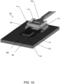
Figure 1A illustrates an example of an optoelectronic device according to the present disclosure; -
Figure 1B illustrates an exploded view of the optoelectronic device ofFigure 1A ; -
Figure 2A illustrates a close-up, top perspective view of the optical socket ofFigure 1A ; -
Figure 2B illustrates a close-up, bottom perspective view of the optical socket ofFigure 1A ; -
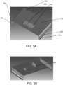
Figure 3A illustrates a close-up, top perspective view of the support member ofFigure 1A ; -
Figure 3B illustrates a close-up, bottom perspective view of the support member ofFigure 1A ; -
Figure 4A illustrates another example of an optoelectronic device according to the present disclosure; -
Figure 4B illustrates yet another example of an optoelectronic device according to the present disclosure; and -
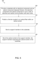
Figure 5 is a flowchart schematically illustrating an example method of manufacturing or assembling an optoelectronic device according to the present disclosure. - Generally, an optoelectronic system or device includes one or more optical connectors to carry, transmit, or propagate optical signals onto or off of the optoelectronic device (e.g., chip, substrate, package, die). The optical connectors may require precisely molded parts or components to provide proper alignment (e.g., micron-level alignment or tolerance) between certain components of the optoelectronic device (e.g., an optical component and an optical ferrule). Because of the high degree of alignment that may be necessary between the components, some parts or assemblies that comprise the optical connector are often difficult to manufacture, and are therefore expensive.
- An example of such a precise part is an optical socket configured to align or optically couple to an optical ferrule, into which are assembled one or more optical fibers, which, in turn, are aligned with respect to an optical component (e.g., disposed on an optoelectronic substrate of an optoelectronic device). The optical socket will typically be precisely aligned and subsequently bonded to an optoelectronic substrate that may include or comprise one or more of an electronic printed circuit board (PCB) or other suitable circuit board (e.g., silicon, organic material), a substrate layer disposed over the circuit board, a silicon interposer, or a combination of an interposer bonded on top of a circuit board or substrate layer. More complex structures, consisting of multiple stacked layers of organic substrates and Si interposers, are also possible. Depending on the system geometry and the method of attachment, an optical socket may be bonded to the substrate (e.g., substrate layer or the circuit board) or to an interposer mounted on top of the substrate. Interposers may come in a variety of sizes, having widths or lengths that may vary from a few mm up to 20 mm or larger. If an optical socket is configured to be bonded or otherwise mounted to the substrate, it may be necessary for the optical socket to straddle the interposer bonded on top of the substrate or circuit board. In this case, a variety of optical socket sizes may be needed to correspond to the variety of interposer sizes available.
- As mentioned earlier, the optical socket generally contains alignment features of extremely high precision. These may be positive or male alignment features such as guide pins (e.g., with diameter tolerance in the range of ±1 µm, and spacing between pairs of guide pins controlled to less than 5 µm). Alignment features in the socket may also be of negative or female form, such as guide holes or slots. When an optical socket incorporates positive alignment features, a ferrule which is mated to it incorporates corresponding negative features. In some implementations, optical sockets with negative alignment features are mated to ferrules with corresponding positive features.
- Optical sockets will typically be manufactured by a process of plastic injection molding or metal forming such as fine blanking or stamping. These processes are used very broadly in the manufacture of electronic components, and are generally among the least expensive manufacturing processes available. However, molding and stamping, for example, are typically not used to produce parts with tolerances in the range of ±1 µm to ±5 µm. Producing such precise parts, as are required for efficient optical data transmission, may require the use of very expensive molding equipment and specialized molding compounds. Metal molds, into which the plastic comprising an optical socket is injected, may contain only 1 or 2 cavities, each of which produces a single part during a molding production cycle. This contrasts to a more standard injection mold which may contain 64 or 128 cavities, thereby increasing production by a factor of 100 times or more per cycle in comparison. Finally the actual molding process must often be done more slowly than usual, to minimize thermal distortion of the resulting optical socket. The process of perfecting such high precision parts is extremely time consuming. Each newly designed component behaves differently than its predecessor, and requires a great deal of expert technical attention to be brought into compliance with specification. Clearly, this combination of factors causes a significant relative increase in the cost of super-high precision molded parts as compared to standard tolerance parts.
- Within these constraints, it is highly desirable to make as few types of high precision parts as practicable and to use existing qualified parts in as many applications as possible. According to the present disclosure, one way to achieve this result is to separate the optical socket into two parts as described herein - a high precision optical socket (e.g., optical socket 114) and a much lower precision support or base member (e.g., support member 116). In this manner, the generally more expensive, high precision optical socket can be used regardless of system geometry, by assembling it in combination with the generally less expensive support member. The support member may be made with various sizes as described herein.
- Besides the benefit of reusing the high precision optical socket, there are additional benefits to bonding the support member to the circuit board or other portion of the substrate as opposed to the interposer mounted on the substrate as described herein in accordance with implementations of the present disclosure. This approach removes the optical socket from the surface of the interposer and transfers the attachment strength to the circuit board or substrate underlying the interposer. The presence of the optical socket on top of or directly attached to the interposer may produce undesirable results due to mechanical stress or induced electrical effects. Additionally, the mechanical bond strength between the optical socket and the substrate may be increased by utilizing additional area on the substrate or circuit board for attachment to the support member that is not available on the interposer. This may be especially important when mechanical forces are applied to an optical cable that exits the ferrule or optical socket which may impact the bond as commonly occurs in this context. The support member may even be solder reflow attached to the substrate or circuit board, providing an extremely robust mechanical attachment.
- Implementations of the present disclosure provide improved optoelectronic devices or methods of manufacturing or assembling the same to provide a precise or high degree of alignment between certain components while efficiently using overall system volume, reducing manufacturing complexity, or reducing manufacturing costs. For example, inexpensive support members of different sizes may be manufactured or constructed to fit various-sized interposers or substrates. One or single-sized optical sockets couplable to such support members may be used to provide the necessary high-precision alignment between the optical ferrule and optical component resident or otherwise disposed on the interposer or circuit board. The inexpensive support member configured to fit a specific-sized interposer or substrate may be assembled to the single-sized optical socket to mount the optical socket to the substrate or interposer accordingly.
-
Figures 1A-1B illustrate an example of an optoelectronic system ordevice 100 according to the present disclosure. Theoptoelectronic device 100 includes a substrate 102 (e.g., an organic substrate layer). Thesubstrate 102 may include a substrate layer disposed over a circuit board. Thesubstrate 102 may serve as a foundation or common carrier for electronic and optical components mounted or otherwise disposed on an interposer 112 (e.g., an optical or electro-optical interposer). One or moreelectronic components 104 and one or moreoptical components 106, such as a lens array, are disposed on theinterposer 112. Theoptoelectronic device 100 may incorporate elements such as waveguides, grating couplers, electro-optical modulators, photodetectors, or other electro-optical components used to convert an electrical signal to a light signal or vice versa. While not specifically illustrated inFigures 1A-1B , theinterposer 112 may include multiple layers (e.g., conducting, semiconductor, dielectric, or insulating layers). Theinterposer 112 may include an insulating layer sandwiched between semiconductor layers. For example, theinterposer 112 may be a silicon-on-insulator (SOI) or a silicon-on-glass substrate. In some implementations, theinterposer 112 includes an insulating layer such as a buried oxide (BOX) layer composed of silicon dioxide or other insulating oxide material. In other implementations, the insulating layer is composed of another insulating material such as sapphire, diamond, or glass. - The one or more
electronic components 104 are in electrical communication with electro-optical components (e.g., incorporated in or on aninterposer 112 or thesubstrate 102 as described in more detail below), which in the transmission mode, transform electrical signals into optical signals which are transmitted through alens array 106 into a ferrule (e.g., ferrule 110). When operating in a receive mode, optical signals are transmitted from the ferrule, on an optical socket (e.g., optical socket 114), into the lens array where the signals are focused onto electro-optical components embedded in the interposer beneath the lens array, converted into electronic signals, and ultimately transferred to theelectronic component 104 for processing. Theoptoelectronic device 100 may include theinterposer 112 to connect (e.g., optically or both electrically and optically) the one or more electronic and optical components as described in more detail below with respect toFigures 4A-4B . The one or moreelectronic components 104 may include, but are not limited to, integrated circuits, processors, chip sets, circuit boards, or combinations thereof. The one or moreoptical components 106 may include, for example, single lenses, lens arrays, fiber stubs, or optical tapers. Electro-optical components integrated into theinterposer 112 orsubstrate 102 may include but are not limited to, light emitters, light detectors, photodetectors, wave guides, modulators, heaters, filters, and combinations thereof. For example, theoptical component 106 may be a lens or lens array configured to collect, collimate, focus, or concentrate optical signals prior to passing the optical signals from the light emitter, to the light detector, or to/from the optical transceiver or an optical fiber optically coupled to the lens or lens array. Vertical cavity surface emitting lasers, light emitting diodes, distributed feedback semiconductor laser diodes, or miniature lasers are examples of commonly used light emitters or sources. Surface illuminated photodiodes, waveguide photodetectors, or phototransistors are examples of commonly used light detectors. - The
optoelectronic device 100 further includes anoptical fiber 108 and aferrule 110 coupled (e.g., opto-mechanically) to theoptical fiber 108. A first end of theoptical fiber 108 may terminate within or otherwise be coupled or bonded to theferrule 110. In some implementations, a second end of theoptical fiber 108 may be coupled to a light emitter, light detector, or optical transceiver (not shown inFigures 1A-1B ) disposed off of or away from thesubstrate 102. Theoptical fiber 108 may carry or transmit optical signals to or from the optical component 106 (e.g., onto or off of the optoelectronic device 100). Theoptical fiber 108 may be a single fiber or an array of fibers. Theoptical fiber 108 may be a single mode, polarization maintaining, or multi-mode optical fiber. - The
optoelectronic device 100 further includes anoptical socket 114 configured (e.g., shaped or dimensioned) to receive and hold theferrule 110 therein. Theoptical socket 114 aligns theferrule 110 and theoptical component 106 when theferrule 110 is received (e.g., positioned, disposed, inserted) therein and theoptical socket 114 is mounted on or to thesubstrate 102 via asupport member 116 as described in more detail below. For example, theoptical fiber 108 coupled to theferrule 110 may be aligned with a lens of theoptical component 106 such that optical signals may be transferred or transmitted from theoptical component 106 to theoptical fiber 108 or vice versa when theferrule 110 is received within theoptical socket 114 and theoptical socket 114 is mounted on or to thesubstrate 102 via asupport member 116. - With reference to close-up views of the
optical socket 114 inFigures 2A-2B , to provide the precise alignment between theferrule 110 and theoptical component 106 as described above, theoptical socket 114 is a precisely molded or manufactured part or component with critical alignment features fabricated with micron tolerances (e.g., of less than ±5 µm, and in some cases ±1 µm). For example, theoptical socket 114 may include areceptacle 220 shaped, sized, or dimensioned to receive theferrule 110. In particular, thereceptacle 220 may have a shape or contour configured to match or mate with a corresponding shape or contour of a body of theferrule 110. - In some implementations, the
optical socket 114 may include one or more alignment features 222 (e.g., mechanical attachment features) configured to mate with corresponding alignment features 111 of theferrule 110 to align theferrule 110 thereto. For example, theoptical socket 114 may include one or more male connector features configured to mate with corresponding female connector features of theferrule 110 or vice versa. Male connector features may include pins, poles, or protrusions and female connector features may include holes, openings, or cavities. In some implementations, theoptical socket 114 may include one or more alignment or connector features 224 configured to mate with corresponding alignment or connector features (e.g., opening or slot 344) of thesupport member 116 as described in more detail below. - Referring back to
Figures 1A-1B , theoptoelectronic device 100 further includes thesupport member 116. As described above, theoptical socket 114 is fixedly mounted on or to thesubstrate 102 via thesupport member 116. Thesupport member 116 is disposed between thesubstrate 102 and theoptical socket 114 such that theoptical socket 114 is spaced from thesubstrate 102 by thesupport member 116. Thesupport member 116 is bonded (e.g., fixedly attached, assembled on, or otherwise physically coupled) to both the substrate 102 (e.g., or interposer 112) and theoptical socket 114 to support theoptical socket 114 on thesubstrate 102 in a fixed position. Thesupport member 116 may provide a base for theoptical socket 114 to sit or be disposed on between theoptical socket 114 and thesubstrate 102. - In some implementations, the
support member 116 is soldered to thesubstrate 102 or adhered to thesubstrate 102 with an adhesive (e.g., curable adhesive or epoxy). Thesupport member 116 may be constructed out of a material able to withstand multiple solder reflow temperature cycles (e.g., up to 270 degrees C) for a limited period of time (e.g., typically less than 1 minute). In some implementations, thesupport member 116 is adhered to theoptical socket 114 with an adhesive (e.g., curable adhesive or epoxy). In other implementations, thesupport member 116 is bonded to theoptical socket 114 using solder or by localized melting of the socket by means of a laser or other focused heating method. - In some implementations, the
support member 116 may provide strain relief between theoptical socket 114 and thesubstrate 102 orinterposer 112 as theoptical socket 114 is not directly coupled or bonded to either thesubstrate 102 orinterposer 112. In other implementations, thesupport member 116 may be constructed out of a material (e.g., metallic material) and act as an electromagnetic shield or radio frequency shield for the optical or electronic components it covers or is disposed over. In some implementations, theoptical socket 114 is removable or detachable from thesupport member 116 without damaging one or more of theoptical interposer 112,substrate 102, oroptical component 106 after theoptical socket 114 is bonded or otherwise attached to thesupport member 116. As such, theoptical socket 114 may be removed from the optoelectronic device to provide modularity (e.g., for repair, inspection, or replacement). - The
support member 116 is a relatively inexpensive part or component to manufacture. For example, in some implementations, thesupport member 116 is constructed out of sheet metal or plastic. Thesupport member 116 may be formed or constructed without being precisely molded or manufactured. That is, thesupport member 116 may be constructed without micron-level tolerance alignment features to align theferrule 110 and theoptical component 106 in contrast with theoptical socket 114. In this manner, manufacturing costs, time, and complexity for thesupport member 116 may be greatly reduced relative to that of theoptical socket 114. Additionally, multiple or various sized or dimensionedsupport members 116 configured to straddleinterposers 112 with different sizes may be made without heavily impacting manufacturing costs. As described in more detail below, single or one sizedoptical sockets 114 may be bonded to supportmembers 116 of different or various sizes to mount theoptical sockets 114 to substrates or interposers having different dimensions. - With reference to
Figures 1A and4A-4B together, theoptical socket 114 is bondable to supportmembers support members support member 116 described herein.Respective interposers optoelectronic devices respective support members respective interposers optical socket 114 may be used with various sized support members to be mounted to substrates or interposers of different sizes. A single SKU may be provided for the relatively more costly to manufactureoptical socket 114 while multiple SKU's can be provided for different sized support members (e.g.,support members - With reference to close-up views of the
support member 116 illustrated inFigures 3A-3B , thesupport member 116 has a substantially U-shaped configuration. Thesupport member 116 may include a support surface 332 (e.g., planar surface) extending between two opposingsidewalls optical socket 114 is bonded to thesupport surface 332 while thesubstrate 102 is bonded to the two opposingsidewalls sidewalls feet substrate 102. Theoptical socket 114 may also incorporate features, such as cylindrical projections, formed on the lower surface that mate with an upper surface ofsupport member surface 116. In this context, corresponding features, such as round holes or elongated slots, will be formed through upper surface ofsupport member 116 to accommodate the locating features on theoptical socket 114. These features may be used to provide coarse alignment between theoptical socket 114 and thesupport member 116 or to increase the attachment strength of the adhesive joint bonding the optical socket to the support member. - The
support member 116 comprises a recessedenclosure 342 extending along two, three, or four sides of theoptical component 106 when thesupport member 116 is bonded to thesubstrate 102. Thisenclosure 342 may act to prevent or reduce the entry of contamination or debris into the optical path between theferrule 110, optical component 106 (e.g., a lens array), and electro-optical components fabricated on the surface of theinterposer 112. Effectiveness ofenclosure 342 as a contamination shield may be enhanced by dispensing a bead of adhesive between a top or upper surface of theinterposer 112 and an opposing surface of theenclosure 342. When the adhesive is cured, it may effectively close off any gap that may exist between theinterposer 112 andsupport member 116, and prevents the entry of all contamination from below theoptical socket 114. A throughopening 344 of the recessedenclosure 342 allows optical signals to pass therethrough between theoptical component 106 and theoptical fiber 108 coupled to theferrule 110. Further, in some implementations, the throughopening 344 may function as the connector feature configured to mate with theconnector feature 224 of theoptical socket 114. For example, theopening 344 may be a slot configured to receive theconnector feature 224 therein. -
Figure 5 illustrates a flowchart of an example method of manufacturing or assembling an optoelectronic device (e.g.,optoelectronic devices method 500 begins atblock 550, wherein thesubstrate 102 with anelectrical component 104 and anoptical component 106 disposed thereon is provided. Theelectrical component 104 andoptical component 106 are configured to be in electrical communication, optical communication, or both optical and electrical communication with each other. Atblock 552, theferrule 110 coupled to theoptical fiber 108 is positioned within theoptical socket 114. Atblock 554, thesupport member 116 is bonded to thesubstrate 102. Atblock 556, the optical socket is bonded to thesupport member 116. Thesupport member 116 supports theoptical socket 114 on thesubstrate 102. In some implementations, thesupport member 116 is bonded to thesubstrate 102 prior to bonding theoptical socket 114 to thesupport member 116. In other implementations, theoptical socket 114 is bonded to thesupport member 116 prior to bonding thesupport member 116 to thesubstrate 102. In some implementations, the method provides alignment between optical transmitting and receiving components of the optoelectronic device as described herein. - The
support member 116 is bonded to thesubstrate 102 and straddles theinterposer 112. In some implementations, themethod 500 may include removing or detaching theoptical socket 114 from thesupport member 116 without damaging thesubstrate 102,optical component 106, or interposer 112 (e.g., to repair, replace, or inspect theoptical socket 114 or other components therein). - In some implementations, the
method 500 may further include passive alignment of, on the one hand, theferrule 110 oroptical socket 114, and, on the other hand, theoptical component 106 or theoptical interposer 112, by using pattern recognition or intelligent machine vision to bring into alignment one or more mechanical alignment features (e.g., correspondingfeatures optical socket 114 to thesupport member 116, or bonding bothsocket 114 andsupport member 116 to thesubstrate 102, having previously bonded thesocket 114 to thesupport member 116. - In some implementations, the
method 500 may further include active alignment of theferrule 110 or theoptical socket 114 and theoptical component 106 or theoptical interposer 112 prior to bonding thesupport member 116 to thesubstrate 102, bonding theoptical socket 114 to thesupport member 116, or both. In such implementations, themethod 500 includes activation of an optical light source (e.g., disposed on or off thesubstrate 100 coupled to theoptical component 106 or theoptical fiber 108, respectively) to emit light between theoptical fiber 108 and theoptical component 106. Themethod 500 further includes moving theoptical socket 114 or theoptical component 106 to a plurality of positions relative to each other. The components may be moved in a plane at an angle (e.g., orthogonal, parallel, or oblique) relative to a path of the light to adjust the path of the light between theoptical fiber 108 and theoptical component 106. For example, when the path of the light between theoptical fiber 108 and theoptical component 106 is perpendicular or orthogonal relative to a top or rear surface ofsubstrate 102, the components may be moved to a plurality of positions in a plane orthogonal to the path of the light (e.g., in a plane parallel to the substrate 102). In some implementations, the components may be moved in a plane extending parallel to the top or rear surface of thesubstrate 102. The method further includes monitoring light throughput at each of the plurality of positions and bonding thesupport member 116 to thesubstrate 102, theoptical socket 114 to thesupport member 116, or both, at the position wherein light throughput is greatest. - In the foregoing description, numerous details are set forth to provide an understanding of the subject disclosed herein. However, implementations may be practiced without some or all of these details. Other implementations may include additions, modifications, or variations from the details discussed above. It is intended that the appended claims cover such modifications and variations. The specification and drawings are, accordingly, to be regarded as illustrative rather than restrictive.
- It will be recognized that the terms "comprising," "including," and "having," as used herein, are specifically intended to be read as open-ended terms of art. The term "or," in reference to a list of two or more items, covers all of the following interpretations of the word: any of the items in the list, all of the items in the list, and any combination of the items in the list. As used herein, the terms "connected," "coupled," or any variant thereof means any connection or coupling, either direct or indirect, between two or more elements; the coupling or connection between the elements can be physical (e.g., mechanical), logical, electrical, optical, or a combination thereof.
- In the Figures, identical reference numbers identify identical, or at least generally similar, elements. To facilitate the discussion of any particular element, the most significant digit or digits of any reference number refers to the Figure in which that element is first introduced. For example,
element 110 is first introduced and discussed with reference toFigure 1 .
Claims (11)
- An optoelectronic device (100; 400a; 400b) comprising:a substrate (102);an optical interposer (112; 412a; 412b) disposed on the substrate (102);an electronic component (104) disposed on the optical interposer (112; 412a; 412b);electro-optical components incorporated in or on the optical interposer or the substrate;an optical component (106) disposed on the optical interposer (112; 412a; 412b), wherein the optical component (106) is in optical communication with the electro-optical components and the electronic component (104) is in electrical communication with theelectro-optical components; an optical fiber (108);a ferrule (110) coupled to the optical fiber (108);an optical socket (114) receiving the ferrule (110) therein, the optical socket (114) being configured to align the ferrule (110) and the optical component (106) when the ferrule (110) is received therein and the optical socket (114) is mounted on the substrate (102), the optical socket (114)being bondable to support members having different dimensions;a support member (116; 416a; 416b) disposed between the substrate (102) and the optical socket such that the optical socket (114) is spaced from the substrate (102) by the support member (116; 416a; 416b), the support member (116)being bonded to the optical socket (114),characterized in thatthe support member (116; 416a; 416b) is also bonded to the substrate (102) to support the optical socket (114) on the substrate (102); andthe support member (116; 416a; 416b) is dimensioned to straddle opposing sides of the optical interposer (112; 412a; 412b) and comprises a substantially U-shapedconfiguration, the support member (116; 416a; 416b) including a support surface (332) extending between two opposing sidewalls (334, 336), the optical socket (114)being bonded to the support surface (332) and the substrate (102) being bonded to the two opposing sidewalls (334, 336), wherein the support member (116; 416a; 416b) comprises a recessed enclosure (344) including walls extending along two or more sides of the optical component (106).
- The optoelectronic device (100; 400a; 400b) of claim 1, wherein the optical component (106) comprises a lens.
- The optoelectronic device (100; 400a; 400b) of claim 1, wherein the substrate (102) comprises a circuit board and the support member (116; 416a; 416b) is bonded to the circuit board.
- The optoelectronic device (100; 400a; 400b) of claim 1, wherein the support member (116; 416a; 416b) is constructed out of one or more of sheet metal, plastic, or a material able to withstand multiple solder reflow temperature cycles, and/or
the support member (116; 416a; 416b) is constructed without micron-level tolerance alignment features to align the ferrule (110) and the optical component (106). - The optoelectronic device (100; 400a; 400b) of claim 1, wherein the support member (116; 416a; 416b) is soldered to the substrate (102) or adhered to the substrate (102) with an adhesive, or
the support member (116; 416a; 416b) is adhered to the optical socket (114) with an adhesive or bonded to the optical socket (114) by localized melting of a portion of the socket or support member (116; 416a; 416b). - The optoelectronic device of claim 1, wherein a through opening of the recessed enclosure allows optical signals to pass therethrough between the optical component and the optical fiber coupled to the ferrule and the walls enclose an optical path between the optical component and the optical fiber to reduce entry of contaminants therein.
- A method (500) of assembling an optoelectronic device (100; 400a; 400b), the method comprising:providing electro-optical components incorporated in or on an optical interposer or a substrate;providing (550) the substrate (102), an electrical component (104) and an optical component (106), wherein the electrical component (104) is in electrical communication with the electro-optical components and the optical component (106) is in optical communication with electro-optical components, wherein the electrical component (104) and the optical component (106) are disposed on the optical interposer (112; 412a; 412b), the optical interposer (112; 412a; 412b) being disposed on the substrate (102);positioning (552) a ferrule (110) coupled to an optical fiber (108) within an optical socket (114), the optical socket (114) being configured to align the ferrule (110) and the optical component (106) when the ferrule (110) is received therein, the optical socket (114) being bondable to support members having different dimensions;
andbonding (556) the optical socket (114) to a support member (116), the support member (116) supporting the optical socket (114), wherein the support member (116; 416a; 416b) is disposed between the substrate (102) and the optical socket (114) such that the optical socket (114) is spaced from the substrate (102) by the support member (116; 416a; 416b);characterized in thatthe method comprises bonding (554) the support member (116; 416a; 416b) to the substrate (102), the support member (116; 416a; 416b) supporting the optical socket (114),wherein the support member (116; 416a; 416b) is dimensioned to straddle opposing sides of the optical interposer (112; 412a; 412b) and comprises a substantially U-shaped configuration, the support member (116; 416a; 416b) including a support surface (332) extending between two opposing sidewalls (334, 336), the optical socket (114) being bonded to the support surface (332) and the substrate (102) being bonded to the two opposing sidewalls (334, 336), wherein the support member (116; 416a; 416b) comprises a recessed enclosure (344) including walls extending along two or more sides of the optical component (106). - The method of claim 7, wherein the support member (116; 416a; 416b) is bonded to the substrate (102) prior to bonding the optical socket (114) to the support member (116; 416a; 416b).
- The method of claim 7, wherein the optical socket (114) is bonded to the support member (116; 416a; 416b) prior to bonding the support member (116; 416a; 416b) to the substrate (102).
- The method of claim 7, further comprising passively aligning the ferrule (110) and the optical component (106) with one or more mechanical alignment features prior to one or both of bonding the support member (116; 416a; 416b) to the substrate (102) and bonding the optical socket (114) to the support member (116; 416a; 416b).
- The method of claim 7, further comprising:
actively aligning the optical socket (114) and the optical component (106) prior to one or both of bonding the support member (116; 416a; 416b) to the substrate (102) and bonding the optical socket (114) to the support member (116; 416a; 416b), comprising:activating an optical light source to emit light between the optical fiber (108) and the optical component (106);moving the optical socket (114) or the optical component (106) to a plurality of positions relative to each other in a plane orthogonal to a path of the light to adjust the path of the light between the optical fiber (108) and the optical component (106);monitoring light throughput at each of the plurality of positions; andbonding one or both of the support member (116; 416a; 416b) to the substrate (102) and the optical socket (114) to the support member (116; 416a; 416b) at the position wherein light throughput is greatest.
Applications Claiming Priority (1)
| Application Number | Priority Date | Filing Date | Title |
|---|---|---|---|
| US16/175,652 US10795103B2 (en) | 2018-10-30 | 2018-10-30 | Optoelectronic device with a support member |
Publications (2)
| Publication Number | Publication Date |
|---|---|
| EP3647846A1 EP3647846A1 (en) | 2020-05-06 |
| EP3647846B1 true EP3647846B1 (en) | 2023-03-22 |
Family
ID=68051717
Family Applications (1)
| Application Number | Title | Priority Date | Filing Date |
|---|---|---|---|
| EP19198971.4A Active EP3647846B1 (en) | 2018-10-30 | 2019-09-23 | Optoelectronic device with a support member |
Country Status (3)
| Country | Link |
|---|---|
| US (1) | US10795103B2 (en) |
| EP (1) | EP3647846B1 (en) |
| CN (1) | CN111123446B (en) |
Families Citing this family (7)
| Publication number | Priority date | Publication date | Assignee | Title |
|---|---|---|---|---|
| US11094602B2 (en) * | 2019-08-09 | 2021-08-17 | Advanced Semiconductor Engineering, Inc. | Semiconductor device package |
| US11287585B2 (en) | 2020-03-11 | 2022-03-29 | Nubis Communications, Inc. | Optical fiber-to-chip interconnection |
| US11391898B2 (en) | 2020-06-12 | 2022-07-19 | Hewlett Packard Enterprise Development Lp | Direct opto-mechanical connection for pluggable optical transceivers |
| US11415763B2 (en) * | 2020-08-07 | 2022-08-16 | Hewlett Packard Enterprise Development Lp | Rigid-plane optical jumper for pluggable optical transceivers |
| US11693814B2 (en) * | 2020-12-18 | 2023-07-04 | Quanta Computer Inc. | Systems and methods for expanding memory access |
| US12461321B2 (en) * | 2021-03-11 | 2025-11-04 | Nubis Communications, Inc. | Optical fiber-to-chip interconnection |
| US12625325B2 (en) | 2023-07-26 | 2026-05-12 | Cisco Technology, Inc. | Optical systems for co-packaged applications |
Family Cites Families (14)
| Publication number | Priority date | Publication date | Assignee | Title |
|---|---|---|---|---|
| US5940562A (en) | 1996-03-12 | 1999-08-17 | Minnesota Mining And Manufacturing Company | Stubless optoelectronic device receptacle |
| DE10043324A1 (en) * | 2000-08-23 | 2002-03-14 | Infineon Technologies Ag | Optoelectronic assembly for multiplexing and / or demultiplexing optical signals |
| CN1216306C (en) | 2001-03-17 | 2005-08-24 | 鸿富锦精密工业(深圳)有限公司 | Optical combination and assembly method thereof |
| US8265432B2 (en) * | 2008-03-10 | 2012-09-11 | International Business Machines Corporation | Optical transceiver module with optical windows |
| CN105629411A (en) | 2008-09-23 | 2016-06-01 | 康宁光缆系统有限公司 | Fiber optic cables and assemblies for fiber toward the subscriber applications |
| US9213152B2 (en) | 2012-01-09 | 2015-12-15 | Cisco Technology Inc. | Releasable fiber connector for opto-electronic assemblies |
| US8876410B2 (en) | 2012-01-11 | 2014-11-04 | Cisco Technology, Inc. | Self-aligning connectorized fiber array assembly |
| AU2015263909B2 (en) * | 2014-05-23 | 2020-10-08 | Cudoquanta Florida, Inc. | Vision-based passive alignment of an optical fiber subassembly to an optoelectronic device |
| US10367284B2 (en) | 2015-07-27 | 2019-07-30 | Hewlett Packard Enterprise Development Lp | Socket to support boards in a spaced relation |
| CN106154453A (en) * | 2016-07-07 | 2016-11-23 | 成都迪谱光电科技有限公司 | The antitorque optical cable that a kind of mechanical strength is high |
| WO2018080106A1 (en) * | 2016-10-26 | 2018-05-03 | 엘에스엠트론 주식회사 | Optical connector |
| US9798087B1 (en) * | 2016-11-01 | 2017-10-24 | Hewlett Packard Enterprise Development Lp | Optoelectronic devices and wavelength-division multiplexing optical connectors |
| WO2018089286A1 (en) | 2016-11-08 | 2018-05-17 | Molex, Llc | Multi-fiber ferrule with lens elements |
| US9995880B1 (en) * | 2017-03-31 | 2018-06-12 | Foxconn Interconnect Technology Limited | Wavelength division multiplexing and demultiplexing in optical communications modules, and methods |
-
2018
- 2018-10-30 US US16/175,652 patent/US10795103B2/en active Active
-
2019
- 2019-09-23 EP EP19198971.4A patent/EP3647846B1/en active Active
- 2019-10-09 CN CN201910951993.3A patent/CN111123446B/en active Active
Also Published As
| Publication number | Publication date |
|---|---|
| EP3647846A1 (en) | 2020-05-06 |
| CN111123446A (en) | 2020-05-08 |
| US20200132953A1 (en) | 2020-04-30 |
| CN111123446B (en) | 2022-04-26 |
| US10795103B2 (en) | 2020-10-06 |
Similar Documents
| Publication | Publication Date | Title |
|---|---|---|
| US10795103B2 (en) | Optoelectronic device with a support member | |
| US11782225B2 (en) | Multi-fiber interface apparatus for photonic integrated circuit | |
| US10942324B2 (en) | Integrated electrical and optoelectronic package | |
| US12379555B2 (en) | Detachable connector for co-packaged optics | |
| EP0968447B1 (en) | Receptacle for direct coupling of optoelectronic elements | |
| EP2839328B1 (en) | Fiber optic modules | |
| TWI534491B (en) | Optical connector, electronic apparatus, and optical connector mounting method | |
| CN111566532B (en) | Surface mount package for single mode electro-optic modules | |
| CN101414032B (en) | Optical module and method for making the same | |
| US6450704B1 (en) | Transparent substrate and hinged optical assembly | |
| EP2598928B1 (en) | Body having a dedicated lens for imaging an alignment feature | |
| US20030053766A1 (en) | Parallel fiber optics communications module | |
| US20190384019A1 (en) | Receptacle bodies for optical chips and optical connections incorporating the same | |
| JP2001507814A (en) | Flexible optical connector assembly | |
| CN1220015A (en) | Optoelectronic device socket and manufacturing method thereof | |
| CN106461891A (en) | Vision-based passive alignment of an optical fiber subassembly to an optoelectronic device | |
| US5500914A (en) | Optical interconnect unit and method or making | |
| US11275222B2 (en) | Solder-aligned optical socket with interposer reference and methods of assembly thereof | |
| EP4726450A1 (en) | Assembly comprising an optical board, a socket and an optical chip |
Legal Events
| Date | Code | Title | Description |
|---|---|---|---|
| PUAI | Public reference made under article 153(3) epc to a published international application that has entered the european phase |
Free format text: ORIGINAL CODE: 0009012 |
|
| STAA | Information on the status of an ep patent application or granted ep patent |
Free format text: STATUS: THE APPLICATION HAS BEEN PUBLISHED |
|
| AK | Designated contracting states |
Kind code of ref document: A1 Designated state(s): AL AT BE BG CH CY CZ DE DK EE ES FI FR GB GR HR HU IE IS IT LI LT LU LV MC MK MT NL NO PL PT RO RS SE SI SK SM TR |
|
| AX | Request for extension of the european patent |
Extension state: BA ME |
|
| STAA | Information on the status of an ep patent application or granted ep patent |
Free format text: STATUS: REQUEST FOR EXAMINATION WAS MADE |
|
| 17P | Request for examination filed |
Effective date: 20200911 |
|
| RBV | Designated contracting states (corrected) |
Designated state(s): AL AT BE BG CH CY CZ DE DK EE ES FI FR GB GR HR HU IE IS IT LI LT LU LV MC MK MT NL NO PL PT RO RS SE SI SK SM TR |
|
| STAA | Information on the status of an ep patent application or granted ep patent |
Free format text: STATUS: EXAMINATION IS IN PROGRESS |
|
| 17Q | First examination report despatched |
Effective date: 20211013 |
|
| GRAP | Despatch of communication of intention to grant a patent |
Free format text: ORIGINAL CODE: EPIDOSNIGR1 |
|
| STAA | Information on the status of an ep patent application or granted ep patent |
Free format text: STATUS: GRANT OF PATENT IS INTENDED |
|
| INTG | Intention to grant announced |
Effective date: 20220928 |
|
| RAP3 | Party data changed (applicant data changed or rights of an application transferred) |
Owner name: HEWLETT PACKARD ENTERPRISE DEVELOPMENT LP |
|
| GRAS | Grant fee paid |
Free format text: ORIGINAL CODE: EPIDOSNIGR3 |
|
| GRAA | (expected) grant |
Free format text: ORIGINAL CODE: 0009210 |
|
| STAA | Information on the status of an ep patent application or granted ep patent |
Free format text: STATUS: THE PATENT HAS BEEN GRANTED |
|
| AK | Designated contracting states |
Kind code of ref document: B1 Designated state(s): AL AT BE BG CH CY CZ DE DK EE ES FI FR GB GR HR HU IE IS IT LI LT LU LV MC MK MT NL NO PL PT RO RS SE SI SK SM TR |
|
| REG | Reference to a national code |
Ref country code: GB Ref legal event code: FG4D |
|
| REG | Reference to a national code |
Ref country code: CH Ref legal event code: EP |
|
| REG | Reference to a national code |
Ref country code: IE Ref legal event code: FG4D |
|
| REG | Reference to a national code |
Ref country code: DE Ref legal event code: R096 Ref document number: 602019026587 Country of ref document: DE |
|
| REG | Reference to a national code |
Ref country code: AT Ref legal event code: REF Ref document number: 1555662 Country of ref document: AT Kind code of ref document: T Effective date: 20230415 |
|
| REG | Reference to a national code |
Ref country code: LT Ref legal event code: MG9D |
|
| REG | Reference to a national code |
Ref country code: NL Ref legal event code: MP Effective date: 20230322 |
|
| PG25 | Lapsed in a contracting state [announced via postgrant information from national office to epo] |
Ref country code: RS Free format text: LAPSE BECAUSE OF FAILURE TO SUBMIT A TRANSLATION OF THE DESCRIPTION OR TO PAY THE FEE WITHIN THE PRESCRIBED TIME-LIMIT Effective date: 20230322 Ref country code: NO Free format text: LAPSE BECAUSE OF FAILURE TO SUBMIT A TRANSLATION OF THE DESCRIPTION OR TO PAY THE FEE WITHIN THE PRESCRIBED TIME-LIMIT Effective date: 20230622 Ref country code: LV Free format text: LAPSE BECAUSE OF FAILURE TO SUBMIT A TRANSLATION OF THE DESCRIPTION OR TO PAY THE FEE WITHIN THE PRESCRIBED TIME-LIMIT Effective date: 20230322 Ref country code: LT Free format text: LAPSE BECAUSE OF FAILURE TO SUBMIT A TRANSLATION OF THE DESCRIPTION OR TO PAY THE FEE WITHIN THE PRESCRIBED TIME-LIMIT Effective date: 20230322 Ref country code: HR Free format text: LAPSE BECAUSE OF FAILURE TO SUBMIT A TRANSLATION OF THE DESCRIPTION OR TO PAY THE FEE WITHIN THE PRESCRIBED TIME-LIMIT Effective date: 20230322 |
|
| REG | Reference to a national code |
Ref country code: AT Ref legal event code: MK05 Ref document number: 1555662 Country of ref document: AT Kind code of ref document: T Effective date: 20230322 |
|
| PG25 | Lapsed in a contracting state [announced via postgrant information from national office to epo] |
Ref country code: SE Free format text: LAPSE BECAUSE OF FAILURE TO SUBMIT A TRANSLATION OF THE DESCRIPTION OR TO PAY THE FEE WITHIN THE PRESCRIBED TIME-LIMIT Effective date: 20230322 Ref country code: NL Free format text: LAPSE BECAUSE OF FAILURE TO SUBMIT A TRANSLATION OF THE DESCRIPTION OR TO PAY THE FEE WITHIN THE PRESCRIBED TIME-LIMIT Effective date: 20230322 Ref country code: GR Free format text: LAPSE BECAUSE OF FAILURE TO SUBMIT A TRANSLATION OF THE DESCRIPTION OR TO PAY THE FEE WITHIN THE PRESCRIBED TIME-LIMIT Effective date: 20230623 Ref country code: FI Free format text: LAPSE BECAUSE OF FAILURE TO SUBMIT A TRANSLATION OF THE DESCRIPTION OR TO PAY THE FEE WITHIN THE PRESCRIBED TIME-LIMIT Effective date: 20230322 |
|
| PG25 | Lapsed in a contracting state [announced via postgrant information from national office to epo] |
Ref country code: SM Free format text: LAPSE BECAUSE OF FAILURE TO SUBMIT A TRANSLATION OF THE DESCRIPTION OR TO PAY THE FEE WITHIN THE PRESCRIBED TIME-LIMIT Effective date: 20230322 Ref country code: RO Free format text: LAPSE BECAUSE OF FAILURE TO SUBMIT A TRANSLATION OF THE DESCRIPTION OR TO PAY THE FEE WITHIN THE PRESCRIBED TIME-LIMIT Effective date: 20230322 Ref country code: PT Free format text: LAPSE BECAUSE OF FAILURE TO SUBMIT A TRANSLATION OF THE DESCRIPTION OR TO PAY THE FEE WITHIN THE PRESCRIBED TIME-LIMIT Effective date: 20230724 Ref country code: ES Free format text: LAPSE BECAUSE OF FAILURE TO SUBMIT A TRANSLATION OF THE DESCRIPTION OR TO PAY THE FEE WITHIN THE PRESCRIBED TIME-LIMIT Effective date: 20230322 Ref country code: EE Free format text: LAPSE BECAUSE OF FAILURE TO SUBMIT A TRANSLATION OF THE DESCRIPTION OR TO PAY THE FEE WITHIN THE PRESCRIBED TIME-LIMIT Effective date: 20230322 Ref country code: AT Free format text: LAPSE BECAUSE OF FAILURE TO SUBMIT A TRANSLATION OF THE DESCRIPTION OR TO PAY THE FEE WITHIN THE PRESCRIBED TIME-LIMIT Effective date: 20230322 |
|
| PG25 | Lapsed in a contracting state [announced via postgrant information from national office to epo] |
Ref country code: SK Free format text: LAPSE BECAUSE OF FAILURE TO SUBMIT A TRANSLATION OF THE DESCRIPTION OR TO PAY THE FEE WITHIN THE PRESCRIBED TIME-LIMIT Effective date: 20230322 Ref country code: PL Free format text: LAPSE BECAUSE OF FAILURE TO SUBMIT A TRANSLATION OF THE DESCRIPTION OR TO PAY THE FEE WITHIN THE PRESCRIBED TIME-LIMIT Effective date: 20230322 Ref country code: IS Free format text: LAPSE BECAUSE OF FAILURE TO SUBMIT A TRANSLATION OF THE DESCRIPTION OR TO PAY THE FEE WITHIN THE PRESCRIBED TIME-LIMIT Effective date: 20230722 |
|
| REG | Reference to a national code |
Ref country code: DE Ref legal event code: R097 Ref document number: 602019026587 Country of ref document: DE |
|
| PLBE | No opposition filed within time limit |
Free format text: ORIGINAL CODE: 0009261 |
|
| STAA | Information on the status of an ep patent application or granted ep patent |
Free format text: STATUS: NO OPPOSITION FILED WITHIN TIME LIMIT |
|
| PG25 | Lapsed in a contracting state [announced via postgrant information from national office to epo] |
Ref country code: SI Free format text: LAPSE BECAUSE OF FAILURE TO SUBMIT A TRANSLATION OF THE DESCRIPTION OR TO PAY THE FEE WITHIN THE PRESCRIBED TIME-LIMIT Effective date: 20230322 Ref country code: DK Free format text: LAPSE BECAUSE OF FAILURE TO SUBMIT A TRANSLATION OF THE DESCRIPTION OR TO PAY THE FEE WITHIN THE PRESCRIBED TIME-LIMIT Effective date: 20230322 Ref country code: CZ Free format text: LAPSE BECAUSE OF FAILURE TO SUBMIT A TRANSLATION OF THE DESCRIPTION OR TO PAY THE FEE WITHIN THE PRESCRIBED TIME-LIMIT Effective date: 20230322 |
|
| 26N | No opposition filed |
Effective date: 20240102 |
|
| REG | Reference to a national code |
Ref country code: DE Ref legal event code: R119 Ref document number: 602019026587 Country of ref document: DE |
|
| REG | Reference to a national code |
Ref country code: CH Ref legal event code: PL |
|
| PG25 | Lapsed in a contracting state [announced via postgrant information from national office to epo] |
Ref country code: LU Free format text: LAPSE BECAUSE OF NON-PAYMENT OF DUE FEES Effective date: 20230923 |
|
| REG | Reference to a national code |
Ref country code: BE Ref legal event code: MM Effective date: 20230930 |
|
| GBPC | Gb: european patent ceased through non-payment of renewal fee |
Effective date: 20230923 |
|
| PG25 | Lapsed in a contracting state [announced via postgrant information from national office to epo] |
Ref country code: LU Free format text: LAPSE BECAUSE OF NON-PAYMENT OF DUE FEES Effective date: 20230923 Ref country code: IT Free format text: LAPSE BECAUSE OF FAILURE TO SUBMIT A TRANSLATION OF THE DESCRIPTION OR TO PAY THE FEE WITHIN THE PRESCRIBED TIME-LIMIT Effective date: 20230322 Ref country code: MC Free format text: LAPSE BECAUSE OF FAILURE TO SUBMIT A TRANSLATION OF THE DESCRIPTION OR TO PAY THE FEE WITHIN THE PRESCRIBED TIME-LIMIT Effective date: 20230322 |
|
| REG | Reference to a national code |
Ref country code: IE Ref legal event code: MM4A |
|
| PG25 | Lapsed in a contracting state [announced via postgrant information from national office to epo] |
Ref country code: IE Free format text: LAPSE BECAUSE OF NON-PAYMENT OF DUE FEES Effective date: 20230923 |
|
| PG25 | Lapsed in a contracting state [announced via postgrant information from national office to epo] |
Ref country code: GB Free format text: LAPSE BECAUSE OF NON-PAYMENT OF DUE FEES Effective date: 20230923 |
|
| PG25 | Lapsed in a contracting state [announced via postgrant information from national office to epo] |
Ref country code: CH Free format text: LAPSE BECAUSE OF NON-PAYMENT OF DUE FEES Effective date: 20230930 |
|
| PG25 | Lapsed in a contracting state [announced via postgrant information from national office to epo] |
Ref country code: IE Free format text: LAPSE BECAUSE OF NON-PAYMENT OF DUE FEES Effective date: 20230923 Ref country code: GB Free format text: LAPSE BECAUSE OF NON-PAYMENT OF DUE FEES Effective date: 20230923 Ref country code: FR Free format text: LAPSE BECAUSE OF NON-PAYMENT OF DUE FEES Effective date: 20230930 Ref country code: DE Free format text: LAPSE BECAUSE OF NON-PAYMENT OF DUE FEES Effective date: 20240403 Ref country code: CH Free format text: LAPSE BECAUSE OF NON-PAYMENT OF DUE FEES Effective date: 20230930 |
|
| PG25 | Lapsed in a contracting state [announced via postgrant information from national office to epo] |
Ref country code: BE Free format text: LAPSE BECAUSE OF NON-PAYMENT OF DUE FEES Effective date: 20230930 |
|
| PG25 | Lapsed in a contracting state [announced via postgrant information from national office to epo] |
Ref country code: BG Free format text: LAPSE BECAUSE OF FAILURE TO SUBMIT A TRANSLATION OF THE DESCRIPTION OR TO PAY THE FEE WITHIN THE PRESCRIBED TIME-LIMIT Effective date: 20230322 |
|
| PG25 | Lapsed in a contracting state [announced via postgrant information from national office to epo] |
Ref country code: BG Free format text: LAPSE BECAUSE OF FAILURE TO SUBMIT A TRANSLATION OF THE DESCRIPTION OR TO PAY THE FEE WITHIN THE PRESCRIBED TIME-LIMIT Effective date: 20230322 |
|
| PG25 | Lapsed in a contracting state [announced via postgrant information from national office to epo] |
Ref country code: CY Free format text: LAPSE BECAUSE OF FAILURE TO SUBMIT A TRANSLATION OF THE DESCRIPTION OR TO PAY THE FEE WITHIN THE PRESCRIBED TIME-LIMIT; INVALID AB INITIO Effective date: 20190923 |
|
| PG25 | Lapsed in a contracting state [announced via postgrant information from national office to epo] |
Ref country code: HU Free format text: LAPSE BECAUSE OF FAILURE TO SUBMIT A TRANSLATION OF THE DESCRIPTION OR TO PAY THE FEE WITHIN THE PRESCRIBED TIME-LIMIT; INVALID AB INITIO Effective date: 20190923 |
|
| PG25 | Lapsed in a contracting state [announced via postgrant information from national office to epo] |
Ref country code: TR Free format text: LAPSE BECAUSE OF FAILURE TO SUBMIT A TRANSLATION OF THE DESCRIPTION OR TO PAY THE FEE WITHIN THE PRESCRIBED TIME-LIMIT Effective date: 20230322 |