EP3647843A1 - Polarization diversity optical interface assembly - Google Patents
Polarization diversity optical interface assembly Download PDFInfo
- Publication number
- EP3647843A1 EP3647843A1 EP19203229.0A EP19203229A EP3647843A1 EP 3647843 A1 EP3647843 A1 EP 3647843A1 EP 19203229 A EP19203229 A EP 19203229A EP 3647843 A1 EP3647843 A1 EP 3647843A1
- Authority
- EP
- European Patent Office
- Prior art keywords
- polarization
- light
- grating couplers
- walk
- crystal
- Prior art date
- Legal status (The legal status is an assumption and is not a legal conclusion. Google has not performed a legal analysis and makes no representation as to the accuracy of the status listed.)
- Granted
Links
Images




Classifications
-
- G—PHYSICS
- G02—OPTICS
- G02B—OPTICAL ELEMENTS, SYSTEMS OR APPARATUS
- G02B6/00—Light guides; Structural details of arrangements comprising light guides and other optical elements, e.g. couplings
- G02B6/24—Coupling light guides
- G02B6/36—Mechanical coupling means
- G02B6/38—Mechanical coupling means having fibre to fibre mating means
- G02B6/3807—Dismountable connectors, i.e. comprising plugs
- G02B6/3833—Details of mounting fibres in ferrules; Assembly methods; Manufacture
- G02B6/3845—Details of mounting fibres in ferrules; Assembly methods; Manufacture ferrules comprising functional elements, e.g. filters
-
- G—PHYSICS
- G02—OPTICS
- G02B—OPTICAL ELEMENTS, SYSTEMS OR APPARATUS
- G02B6/00—Light guides; Structural details of arrangements comprising light guides and other optical elements, e.g. couplings
- G02B6/24—Coupling light guides
- G02B6/26—Optical coupling means
- G02B6/27—Optical coupling means with polarisation selective and adjusting means
- G02B6/2726—Optical coupling means with polarisation selective and adjusting means in or on light guides, e.g. polarisation means assembled in a light guide
- G02B6/2733—Light guides evanescently coupled to polarisation sensitive elements
-
- G—PHYSICS
- G02—OPTICS
- G02B—OPTICAL ELEMENTS, SYSTEMS OR APPARATUS
- G02B6/00—Light guides; Structural details of arrangements comprising light guides and other optical elements, e.g. couplings
- G02B6/10—Light guides; Structural details of arrangements comprising light guides and other optical elements, e.g. couplings of the optical waveguide type
- G02B6/12—Light guides; Structural details of arrangements comprising light guides and other optical elements, e.g. couplings of the optical waveguide type of the integrated circuit kind
- G02B6/122—Basic optical elements, e.g. light-guiding paths
- G02B6/124—Geodesic lenses or integrated gratings
-
- G—PHYSICS
- G02—OPTICS
- G02B—OPTICAL ELEMENTS, SYSTEMS OR APPARATUS
- G02B6/00—Light guides; Structural details of arrangements comprising light guides and other optical elements, e.g. couplings
- G02B6/10—Light guides; Structural details of arrangements comprising light guides and other optical elements, e.g. couplings of the optical waveguide type
- G02B6/12—Light guides; Structural details of arrangements comprising light guides and other optical elements, e.g. couplings of the optical waveguide type of the integrated circuit kind
- G02B6/126—Light guides; Structural details of arrangements comprising light guides and other optical elements, e.g. couplings of the optical waveguide type of the integrated circuit kind using polarisation effects
-
- G—PHYSICS
- G02—OPTICS
- G02B—OPTICAL ELEMENTS, SYSTEMS OR APPARATUS
- G02B6/00—Light guides; Structural details of arrangements comprising light guides and other optical elements, e.g. couplings
- G02B6/24—Coupling light guides
- G02B6/26—Optical coupling means
- G02B6/27—Optical coupling means with polarisation selective and adjusting means
- G02B6/2706—Optical coupling means with polarisation selective and adjusting means as bulk elements, i.e. free space arrangements external to a light guide, e.g. polarising beam splitters
-
- G—PHYSICS
- G02—OPTICS
- G02B—OPTICAL ELEMENTS, SYSTEMS OR APPARATUS
- G02B6/00—Light guides; Structural details of arrangements comprising light guides and other optical elements, e.g. couplings
- G02B6/24—Coupling light guides
- G02B6/26—Optical coupling means
- G02B6/27—Optical coupling means with polarisation selective and adjusting means
- G02B6/2753—Optical coupling means with polarisation selective and adjusting means characterised by their function or use, i.e. of the complete device
- G02B6/2773—Polarisation splitting or combining
-
- G—PHYSICS
- G02—OPTICS
- G02B—OPTICAL ELEMENTS, SYSTEMS OR APPARATUS
- G02B6/00—Light guides; Structural details of arrangements comprising light guides and other optical elements, e.g. couplings
- G02B6/24—Coupling light guides
- G02B6/26—Optical coupling means
- G02B6/30—Optical coupling means for use between fibre and thin-film device
-
- G—PHYSICS
- G02—OPTICS
- G02B—OPTICAL ELEMENTS, SYSTEMS OR APPARATUS
- G02B6/00—Light guides; Structural details of arrangements comprising light guides and other optical elements, e.g. couplings
- G02B6/24—Coupling light guides
- G02B6/26—Optical coupling means
- G02B6/34—Optical coupling means utilising prism or grating
-
- G—PHYSICS
- G02—OPTICS
- G02B—OPTICAL ELEMENTS, SYSTEMS OR APPARATUS
- G02B6/00—Light guides; Structural details of arrangements comprising light guides and other optical elements, e.g. couplings
- G02B6/24—Coupling light guides
- G02B6/36—Mechanical coupling means
- G02B6/38—Mechanical coupling means having fibre to fibre mating means
- G02B6/3807—Dismountable connectors, i.e. comprising plugs
- G02B6/3833—Details of mounting fibres in ferrules; Assembly methods; Manufacture
- G02B6/3853—Lens inside the ferrule
-
- G—PHYSICS
- G02—OPTICS
- G02B—OPTICAL ELEMENTS, SYSTEMS OR APPARATUS
- G02B6/00—Light guides; Structural details of arrangements comprising light guides and other optical elements, e.g. couplings
- G02B6/24—Coupling light guides
- G02B6/36—Mechanical coupling means
- G02B6/38—Mechanical coupling means having fibre to fibre mating means
- G02B6/3807—Dismountable connectors, i.e. comprising plugs
- G02B6/3873—Connectors using guide surfaces for aligning ferrule ends, e.g. tubes, sleeves, V-grooves, rods, pins, balls
- G02B6/3885—Multicore or multichannel optical connectors, i.e. one single ferrule containing more than one fibre, e.g. ribbon type
-
- G—PHYSICS
- G02—OPTICS
- G02B—OPTICAL ELEMENTS, SYSTEMS OR APPARATUS
- G02B6/00—Light guides; Structural details of arrangements comprising light guides and other optical elements, e.g. couplings
- G02B6/24—Coupling light guides
- G02B6/42—Coupling light guides with opto-electronic elements
- G02B6/4201—Packages, e.g. shape, construction, internal or external details
- G02B6/4204—Packages, e.g. shape, construction, internal or external details the coupling comprising intermediate optical elements, e.g. lenses, holograms
- G02B6/4213—Packages, e.g. shape, construction, internal or external details the coupling comprising intermediate optical elements, e.g. lenses, holograms the intermediate optical elements being polarisation selective optical elements
-
- G—PHYSICS
- G02—OPTICS
- G02B—OPTICAL ELEMENTS, SYSTEMS OR APPARATUS
- G02B6/00—Light guides; Structural details of arrangements comprising light guides and other optical elements, e.g. couplings
- G02B6/10—Light guides; Structural details of arrangements comprising light guides and other optical elements, e.g. couplings of the optical waveguide type
- G02B6/12—Light guides; Structural details of arrangements comprising light guides and other optical elements, e.g. couplings of the optical waveguide type of the integrated circuit kind
- G02B2006/12133—Functions
- G02B2006/12147—Coupler
Definitions
- Optoelectronic communication (e.g., using optical signals to transmit electronic data) is becoming more prevalent as a potential solution, at least in part, to the ever increasing demand for high bandwidth, high quality, and low power consumption data transfer in applications such as high performance computing systems, large capacity data storage servers, and network devices.
- Optoelectronic systems or devices such as photonic integrated circuits (PICs) may be used to convert, transmit, or process the optical signals or electronic data.
- Optical signals may be carried, transmitted, or propagated on or off a board or substrate of the PIC via various transmission media including one or more optical fibers. Efficient coupling of light or optical signals to and from the one or more optical fibers is an important aspect of PIC connector design.
- Optical fibers may be used to carry or transmit light or optical signals to and from a PIC. Therefore, efficient coupling of light or optical signals to and from the one or more optical fibers is an important aspect of PIC connector design.
- single mode optical fibers present unique challenges due to the two orthogonal polarization modes supported by such fibers which should be considered when designing optical connectors between such fibers and the PIC.
- PSGCs Polarization splitting grating couplers
- PICs Polarization splitting grating couplers
- the coupling efficiency of PSGCs to single mode optical fibers may be poor having peak insertion losses generally greater than about 5 dB.
- Polarization independent grating couplers may also offer a potential solution.
- design and fabrication of such polarization independent grating couplers remain challenging with respect to achieving wide optical bandwidth and low peak insertion loss.
- a polarization diversity optical interface assembly including a walk-off crystal may be configured to separate the polarization modes of a single mode optical fiber to be coupled to single polarization grating couplers in an efficient manner as described herein.
- Implementations of the present disclosure provide improved polarization diversity optical interface assemblies and methods thereof to couple light (e.g., optical signals) between a single mode optical fiber and single polarization first and second grating couplers to achieve efficient coupling, low peak insertion loss, or wide optical bandwidth.
- light e.g., optical signals
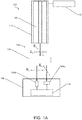
- FIGS 1A-1D illustrate an example of a polarization diversity optical interface assembly 100 and components thereof according to the present disclosure.
- the polarization diversity optical interface assembly 100 includes one or more single mode optical fiber(s) 102, grating couplers 104 (e.g., identified individually as a first grating coupler 104a and a second grating coupler 104b) disposed on a substrate 106, and an optical connector 110 configured to couple light (e.g., optical signals) between the single mode optical fiber 102 and the first and second grating couplers 104a and 104b.
- light e.g., optical signals
- Each of the first and second grating couplers 104a and 104b may be coupled to a waveguide 108 (e.g., identified individually as a first waveguide 108a and a second waveguide 108b, respectively).
- the grating couplers 104 may each be single polarization grating couplers.
- the waveguides 108 may each be polarization dependent or sensitive waveguides.
- the waveguides 108 may transmit light to or from the optical fiber 102.
- the waveguides 108 may transmit optical signals from the optical fiber 102 across the substrate 106 to an optoelectronic device 114 (e.g., a light emitter, detector, modulator, or optical transceiver) disposed on the substrate 106 to receive, detect, or process such signals.
- the waveguides 108 may transmit optical signals from the optoelectronic device 114 off or away from the substrate 106 onto the optical fiber 102 (e.g., via the grating couplers 104 and optical connector 110) to be received, detected, or processed by an optoelectronic device disposed off the substrate 106.
- waveguides 108a and 108b are integrated or monolithically formed with respective grating couplers 104a and104b (e.g., a waveguide grating coupler). In other implementations, the waveguides 108 and grating couplers 104 are separately formed.
- the single mode optical fiber 102 may also be coupled to an optoelectronic device 112 (e.g., a light emitter, detector, modulator, or optical transceiver) disposed off the substrate 106.
- the optical fiber 102 may transmit light or optical signals from the optoelectronic device 112 onto the substrate 106 (e.g., into the waveguides 108 via the optical connector 110 and grating couplers 104) to be received, detected, or processed by the optoelectronic device 114 disposed on the substrate 106.
- optical signals may be carried or transmitted off the substrate 106 by the optical fiber 102 from the optoelectronic 114 device disposed on the substrate 106 as described above.
- the single mode optical fiber 102 may be a single optical fiber or an array of optical fibers.
- the optical connector 110 couples light between the single mode optical fiber 102 and each of the first and second grating couplers 104a and 104b.
- the optical connector 110 includes a ferrule 116 coupled to at least a portion of the single mode optical fiber 102.
- the optical connector 110 further includes a walk-off crystal 118.
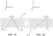
- the walk-off crystal 118 may spatially separate the light into first and second orthogonal polarization modes (e.g., identified individually as E x and E y ) prior to passing the polarization modes through the respective first and second grating couplers 104a and 104b, combine the first and second polarization modes of the light E x and E y (e.g., from the respective first and second grating couplers 104a and 104b) into a single optical output signal prior to passing the light into the single mode optical fiber 102, or both.
- the optical connector 110 may be a single mode expanded beam optical connector.
- the optical connector 110 may include a lens 230 coupled to or disposed at an end of the single mode optical fiber 102 to collimate the light exiting or emerging from the single mode optical fiber 102 as described in more detail below (see Figures 2A-2E ).
- the first and second grating couplers 104a and 104b may extend co-planar with each other.
- the grating couplers 104 may extend along a same horizontal plane or surface of substrate 106 (e.g., a top or front side or bottom or rear side of substrate 106).
- the first and second grating couplers 104a and 104b may also extend or be oriented at an angle (e.g., orthogonal or non-oblique) relative to each other to ensure the first and second orthogonal polarization modes propagate in the proper orientations or directions across the grating couplers 104 (e.g., along optical beam axes of the grating couplers).
- the first grating coupler 104a may extend orthogonally relative to the second grating coupler 104b such that a direction of the light or beam path of the first polarization mode E x propagates across the first grating coupler 104a in a direction (e.g., east-west direction) orthogonal to a direction (e.g., north-south direction) that the light or beam path of the second polarization mode E y propagates across the second grating coupler 104b.
- a direction of the light or beam path of the first polarization mode E x propagates across the first grating coupler 104a in a direction (e.g., east-west direction) orthogonal to a direction (e.g., north-south direction) that the light or beam path of the second polarization mode E y propagates across the second grating coupler 104b.
- the optical connector 110 may include one or more lenses or tilt elements 232 (see Figures 2A-2E ), such as a prism to ensure proper propagation or orientation of the light or beam path from the first and second polarization modes along respective optical beam axes of respective grating couplers 104a and 104b, as described in more detail below.
- lenses or tilt elements 232 such as a prism to ensure proper propagation or orientation of the light or beam path from the first and second polarization modes along respective optical beam axes of respective grating couplers 104a and 104b, as described in more detail below.
- the light from the first and second polarization modes E x and E y may have the same polarization or orientation once they are in their respective waveguides 108 (e.g., waveguides 108 may have one or more turns or bends 120 such that the polarizations or beam path directions are the same or parallel).
- ends of the grating couplers 104 may be spaced apart as illustrated.
- the walk-off crystal 118 spatially separates or combines the first and second polarization modes of the light E x and E y .
- the walk-off crystal 118 may provide angular walk-off ( Figure 1C ) or position walk-off ( Figure 1D ) to separate (or combine) the polarization modes.
- the walk-off crystal 118 may be constructed from a birefringent crystal such as TiO 2 or YVO 4 .
- the degree or amount of angular or position walk-off 118 may be achieved by cutting or shaping the walk-off crystal 118 at a desired angle, orienting the walk-off crystal 118 relative to incoming or outgoing light, or orienting incoming or outgoing light with respect to a crystal optic axis of the walk-off crystal 118 to have a desired angle of incidence.
- the walk-off crystal 118 may include only a single crystal. In other implementations, the walk-off crystal 118 may include two or more crystals.
- a thickness T of the walk-off crystal 118 is selected such that a walk-off distance between the first and second polarization modes of the light E x and E y matches a spacing X (e.g., Figure 1B ) between optical axes of grating couplers 104.
- a thickness of walk-off crystal 118 is selected such that a walk-off distance between the first and second polarization modes of the light E x and E y matches a spacing between axes of lenses (e.g., lenses 232) configured to tilt or focus the light onto the grating couplers 104.
- the walk-off crystal 118 has a thickness between 1 mm to 2.5 mm which may provide or correspond to a walk-off distance between 100 microns to 250 microns between the first and second polarization modes of the light E x and E y .
- the substrate 106 may serve as a foundation or common carrier for various electronic and optical components of a PIC including the grating couplers 104a and 104b in which light is coupled from the single mode optical fiber 102 by the optical connector 110.
- the substrate 106 is constructed out of silicon, thus providing a silicon photonics platform.
- the substrate 106 includes a silicon photonic interposer on which the various electronic and optical components may be disposed.
- the substrate 106 may include multiple layers (e.g., semiconductor, dielectric, or insulating layers).
- the substrate 106 may include an insulating layer sandwiched between semiconductor layers.
- the substrate 106 may be a silicon-on-insulator (SOI), a silicon-on-glass, silicon on sapphire, or silicon on nothing substrate.
- the substrate 106 includes an insulating layer such as a buried oxide (BOX) layer composed of silicon dioxide or other insulating oxide material.
- BOX buried oxide
- the grating couplers 104a and 104b may be disposed on the BOX layer with the BOX layer disposed over or on a base silicon substrate layer of the substrate 106.
- the insulating layer may be composed of another insulating material such as sapphire, diamond, or glass.
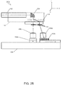
- polarization diversity optical interface assemblies 200a-200e examples are illustrated according to the present disclosure with a walk-off crystal positioned at various locations along the optical path or train relative the other components.
- the polarization diversity optical interface assemblies 200a-200e may include one or more of any of the features described herein with respect to the polarization diversity optical interface assembly 100 or with respect to one another, in whole or in part.
- the polarization diversity optical interface assemblies 200a-200e may include the single mode optical fiber 102, grating couplers 104 and waveguides 108 disposed on a substrate 106, optoelectronic devices 112 or 114 disposed on or off the substrate 106, or optical connector 110 with ferrule 116 as described herein.
- the polarization diversity optical interface assembly 200a includes the lens 230 to collimate light exiting the single mode optical fiber 106 (or focus light entering the single mode optical fiber 106).
- An optical turning element 234 e.g., internal reflection mirror, parabolic turning mirror
- the walk-off crystal 118 is disposed after the optical turning element 234 along the optical path.
- the walk-off crystal 118 may be positioned or disposed at other various locations along the optical path or train between the single mode optical fiber 102 and the grating couplers 104 (e.g., before the optical turning element 234, within the ferrule 116, outside the ferrule 116, disposed on the substrate 106, between the one or more lenses 236 and the grating couplers 104).
- the first and second polarization modes of the light E x and E y may be tilted or oriented to ensure the modes propagate along optical axes of the respective grating couplers 104a and 104b.
- the polarization diversity optical interface assembly 200a may include one or more light tilting lenses or elements 232 identified individually as 232a and 232b (e.g., beam tilting prisms).
- the polarization diversity optical interface assembly 200a may include one or more lenses 236 identified individual as 236a and 236b (e.g., disposed, mounted, or established on the substrate 106) instead of or in addition to the tilting elements 232.
- the one or more lenses 236 may be spherical or aspherical lenses.
- the one or more lenses 236 may focus, tilt, or focus and tilt the first and second polarization modes of the light E x and E y onto the grating couplers 104a and 104b such that light propagates along the optical axes of the respective grating couplers. As described above, the light may then enter respective waveguides 108a and 108b to be carried to optoelectronic device 114 disposed on the substrate 106 to be further processed. For example, the light may be carried to a data modulation system, polarization diversity circuit, or other photonic integrated circuit.
- the walk-off crystal 118 of polarization diversity optical interface assembly 200b may be positioned within the ferrule 116.
- the walk-off crystal 118 is positioned or disposed after the optical turning element 234 similar to polarization diversity optical interface assembly 200a.
- first and second tilting elements 232 disposed on or coupled to the ferrule 116 may tilt or orient the respective light paths of each mode such that they propagate in proper directions (e.g., east-west and north-south when the grating couplers are orthogonal to each other) along optical axes of grating couplers 104 as described above.
- the first polarization mode is tilted about an x-axis while the second polarization mode is tilted about a y-axis prior to entering respective grating couplers 104a and 104b (e.g., at the optimum angle of incidence).
- the tilted first and second polarization modes of the light E x and E y may then pass through respective lenses 236a and 236b to be focused onto the grating couplers 104a and 104b (e.g., to ensure mode matching to the grating coupler and they reach the grating couplers at the optimum angle of incidence).
- the lenses 236a and 236b may be mounted on the substrate 106.
- the walk-off crystal 118 of polarization diversity optical interface assembly 200c may be positioned within the ferrule 116 before the optical turning element 234 such that the first and second polarization modes of the light E x and E y are spatially separated along the optical path prior to being turned by the optical turning element 234.
- the walk-off crystal 118 may be positioned or disposed outside or off of the ferrule 116.
- the walk-off crystal 118 of polarization diversity optical interface assembly 200d may be positioned between one or more lenses 236 and grating couplers 104a and 104b.
- the walk-off crystal 118 may be established or disposed on the substrate 106.
- the one or more lenses 236 may be disposed on the substrate 106 or coupled to the ferrule 116.
- the polarization diversity optical interface assembly 200d may further includes one or more tilting elements 232 as described herein between the walk-off crystal 118 and the grating couplers 104a and 104b.
- the polarization diversity optical interface assembly 200e includes a single lens 236 disposed after the walk-off crystal 118 to focus or orient the first and second polarization modes of the light E x and E y onto and along optical axes of the grating couplers 104a and 104b.
- the polarization diversity optical interface assembly 200e may further include tilting elements 232 to further ensure that the first and second polarization modes of the light E x and E y propagate along the optical axes of grating couplers 104a and 104b.
- the walk-off crystal 118 may be disposed at any of the locations as described herein.
- any of the polarization diversity optical interface assemblies described herein may include an optical connector 310 with a ferrule 316 configured to carry or couple to an array 350 of single mode optical fibers 102a-102d.
- the walk-off crystal 318 may extend across the entire array 350 to spatially separate the light from each fiber 102 into first and second polarization modes prior to passing through pairs of corresponding grating couplers 104.
- multiple spaced apart walk-off crystals 318 may be located between each fiber 102a-102d and grating couplers.
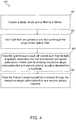
- Figure 4 is a flowchart illustrating a method of coupling light between a single mode optical fiber and single polarization first and second grating couplers with a polarization diversity optical interface assembly (e.g., 100, 200a-200e, 300) according to the present disclosure.
- the method 400 begins at block 460, wherein a single mode optical fiber is coupled to a ferrule.
- bock 462 light is emitted from an optoelectronic device through the single mode optical fiber.
- the light is then passed through a walk-off crystal such that the light is spatially separated into first and second orthogonal polarization modes prior to entering respective single polarization first and second grating couplers disposed on a substrate in block 464.
- the first and second polarization modes are passed through the respective single polarization first and second grating couplers.
- the method 400 further includes passing the first and second polarization modes through first and second polarization dependent waveguides coupled to the respective single polarization first and second grating couplers after passing the first and second polarization modes through the respective single polarization first and second grating couplers.
- the light is passed through the walk-off crystal such that the light is spatially split into the first and second polarization components prior to exiting the ferrule.
- the method 400 further includes passing the first and second polarization modes through respective first and second light tilting elements to orient the first and second polarization modes to propagate along respective optical axes of the respective single polarization first and second grating couplers.
- the method 400 further includes passing the first and second polarization modes through one or more lenses mounted on the substrate to focus the first and second polarization modes onto the respective single polarization first and second grating couplers.
- Optoelectronic devices 112 and 114 such as light emitters, modulators, or photodetectors described herein may include, but are not limited to, vertical cavity surface emitting lasers, distributed feedback lasers, mach-zehnder or ring modulators, or p-i-n or avalanche photodiodes.
- the terms “comprising,” “including,” and “having,” as used herein, are specifically intended to be read as open-ended terms of art.
- the term “or,” in reference to a list of two or more items, covers all of the following interpretations of the word: any of the items in the list, all of the items in the list, and any combination of the items in the list.
- the terms “connected,” “coupled,” or any variant thereof means any connection or coupling, either direct or indirect, between two or more elements; the coupling or connection between the elements can be physical, mechanical, logical, optical, electrical, or a combination thereof.
Landscapes
- Physics & Mathematics (AREA)
- General Physics & Mathematics (AREA)
- Optics & Photonics (AREA)
- Engineering & Computer Science (AREA)
- Microelectronics & Electronic Packaging (AREA)
- Optical Integrated Circuits (AREA)
- Optical Couplings Of Light Guides (AREA)
Abstract
Description
- Optoelectronic communication (e.g., using optical signals to transmit electronic data) is becoming more prevalent as a potential solution, at least in part, to the ever increasing demand for high bandwidth, high quality, and low power consumption data transfer in applications such as high performance computing systems, large capacity data storage servers, and network devices. Optoelectronic systems or devices such as photonic integrated circuits (PICs) may be used to convert, transmit, or process the optical signals or electronic data. Optical signals may be carried, transmitted, or propagated on or off a board or substrate of the PIC via various transmission media including one or more optical fibers. Efficient coupling of light or optical signals to and from the one or more optical fibers is an important aspect of PIC connector design.
- Certain examples are described in the following detailed description and in reference to the drawings, in which:
-
Figure 1A schematically illustrates an example of a polarization diversity optical interface assembly according to the present disclosure; -
Figure 1B illustrates a close-up view of an example of the grating couplers ofFigure 1A ; -
Figures 1C and 1D illustrate close-up views of examples of the walk-off crystal separating the polarization modes of the single mode optical fiber ofFigure 1A ; -
Figure 2A schematically illustrates another example of a polarization diversity optical interface assembly according to the present disclosure; -
Figure 2B illustrates another example of a polarization diversity optical interface assembly according to the present disclosure; -
Figure 2C schematically illustrates another example of a polarization diversity optical interface assembly according to the present disclosure; -
Figure 2D schematically illustrates another example of a polarization diversity optical interface assembly according to the present disclosure; -
Figure 2E schematically illustrates another example of a polarization diversity optical interface assembly according to the present disclosure; -
Figure 3 schematically illustrates yet another example of a polarization diversity optical interface assembly according to the present disclosure; and -
Figure 4 is a flowchart schematically illustrating an example method of coupling light between a single mode optical fiber and single polarization first and second grating couplers with a polarization diversity optical interface assembly according to the present disclosure. - Optical fibers may be used to carry or transmit light or optical signals to and from a PIC. Therefore, efficient coupling of light or optical signals to and from the one or more optical fibers is an important aspect of PIC connector design. In particular, single mode optical fibers present unique challenges due to the two orthogonal polarization modes supported by such fibers which should be considered when designing optical connectors between such fibers and the PIC.
- While single-mode polarization-maintaining fibers are available, they are generally more costly relative to single mode optical fibers. Additionally, such single mode polarization maintaining fibers may need to be "keyed" to align the transmitted polarization modes at a receiver component. Polarization splitting grating couplers (PSGCs) are also presently available which may be used to couple optical signals from single mode optical fibers to the PIC. However, the coupling efficiency of PSGCs to single mode optical fibers may be poor having peak insertion losses generally greater than about 5 dB. Polarization independent grating couplers may also offer a potential solution. However, design and fabrication of such polarization independent grating couplers remain challenging with respect to achieving wide optical bandwidth and low peak insertion loss.
- Typically, single polarization grating couplers are relatively more simple to design and fabricate with wide optical bandwidth and low peak insertion loss (e.g., generally less than about 1.5 dB). Therefore, there remains a need for improvements in efficiently coupling a single mode optical fiber to single polarization grating couplers. A polarization diversity optical interface assembly including a walk-off crystal may be configured to separate the polarization modes of a single mode optical fiber to be coupled to single polarization grating couplers in an efficient manner as described herein. Implementations of the present disclosure provide improved polarization diversity optical interface assemblies and methods thereof to couple light (e.g., optical signals) between a single mode optical fiber and single polarization first and second grating couplers to achieve efficient coupling, low peak insertion loss, or wide optical bandwidth.
-
Figures 1A-1D illustrate an example of a polarization diversityoptical interface assembly 100 and components thereof according to the present disclosure. The polarization diversityoptical interface assembly 100 includes one or more single mode optical fiber(s) 102, grating couplers 104 (e.g., identified individually as afirst grating coupler 104a and asecond grating coupler 104b) disposed on asubstrate 106, and anoptical connector 110 configured to couple light (e.g., optical signals) between the single modeoptical fiber 102 and the first andsecond grating couplers - Each of the first and
second grating couplers first waveguide 108a and asecond waveguide 108b, respectively). Thegrating couplers 104 may each be single polarization grating couplers. The waveguides 108 may each be polarization dependent or sensitive waveguides. The waveguides 108 may transmit light to or from theoptical fiber 102. For example, the waveguides 108 may transmit optical signals from theoptical fiber 102 across thesubstrate 106 to an optoelectronic device 114 (e.g., a light emitter, detector, modulator, or optical transceiver) disposed on thesubstrate 106 to receive, detect, or process such signals. In other implementations, the waveguides 108 may transmit optical signals from theoptoelectronic device 114 off or away from thesubstrate 106 onto the optical fiber 102 (e.g., via thegrating couplers 104 and optical connector 110) to be received, detected, or processed by an optoelectronic device disposed off thesubstrate 106. In some implementations,waveguides respective grating couplers 104a and104b (e.g., a waveguide grating coupler). In other implementations, the waveguides 108 andgrating couplers 104 are separately formed. - The single mode
optical fiber 102 may also be coupled to an optoelectronic device 112 (e.g., a light emitter, detector, modulator, or optical transceiver) disposed off thesubstrate 106. In this manner, theoptical fiber 102 may transmit light or optical signals from theoptoelectronic device 112 onto the substrate 106 (e.g., into the waveguides 108 via theoptical connector 110 and grating couplers 104) to be received, detected, or processed by theoptoelectronic device 114 disposed on thesubstrate 106. In other implementations, optical signals may be carried or transmitted off thesubstrate 106 by theoptical fiber 102 from the optoelectronic 114 device disposed on thesubstrate 106 as described above. The single modeoptical fiber 102 may be a single optical fiber or an array of optical fibers. - The
optical connector 110 couples light between the single modeoptical fiber 102 and each of the first andsecond grating couplers optical connector 110 includes aferrule 116 coupled to at least a portion of the single modeoptical fiber 102. Theoptical connector 110 further includes a walk-offcrystal 118. The walk-offcrystal 118 may spatially separate the light into first and second orthogonal polarization modes (e.g., identified individually as Ex and Ey) prior to passing the polarization modes through the respective first andsecond grating couplers second grating couplers optical fiber 102, or both. Theoptical connector 110 may be a single mode expanded beam optical connector. For example, theoptical connector 110 may include alens 230 coupled to or disposed at an end of the single modeoptical fiber 102 to collimate the light exiting or emerging from the single modeoptical fiber 102 as described in more detail below (seeFigures 2A-2E ). - Referring to
Figure 1B , the first andsecond grating couplers grating couplers 104 may extend along a same horizontal plane or surface of substrate 106 (e.g., a top or front side or bottom or rear side of substrate 106). In some implementations, the first andsecond grating couplers first grating coupler 104a may extend orthogonally relative to thesecond grating coupler 104b such that a direction of the light or beam path of the first polarization mode Ex propagates across thefirst grating coupler 104a in a direction (e.g., east-west direction) orthogonal to a direction (e.g., north-south direction) that the light or beam path of the second polarization mode Ey propagates across thesecond grating coupler 104b. In other implementations, theoptical connector 110 may include one or more lenses or tilt elements 232 (seeFigures 2A-2E ), such as a prism to ensure proper propagation or orientation of the light or beam path from the first and second polarization modes along respective optical beam axes ofrespective grating couplers - The light from the first and second polarization modes Ex and Ey may have the same polarization or orientation once they are in their respective waveguides 108 (e.g., waveguides 108 may have one or more turns or
bends 120 such that the polarizations or beam path directions are the same or parallel). In some implementations, ends of thegrating couplers 104 may be spaced apart as illustrated. - Referring to
Figures 1C-1D and as described above, the walk-offcrystal 118 spatially separates or combines the first and second polarization modes of the light Ex and Ey. The walk-offcrystal 118 may provide angular walk-off (Figure 1C ) or position walk-off (Figure 1D ) to separate (or combine) the polarization modes. The walk-offcrystal 118 may be constructed from a birefringent crystal such as TiO2 or YVO4. The degree or amount of angular or position walk-off 118 (e.g., between 5 and 10 degrees or between 0.1 to 0.2 radians) may be achieved by cutting or shaping the walk-offcrystal 118 at a desired angle, orienting the walk-offcrystal 118 relative to incoming or outgoing light, or orienting incoming or outgoing light with respect to a crystal optic axis of the walk-offcrystal 118 to have a desired angle of incidence. In some implementations, the walk-offcrystal 118 may include only a single crystal. In other implementations, the walk-offcrystal 118 may include two or more crystals. - In some implementations, a thickness T of the walk-off
crystal 118 is selected such that a walk-off distance between the first and second polarization modes of the light Ex and Ey matches a spacing X (e.g.,Figure 1B ) between optical axes ofgrating couplers 104. In other implementations, a thickness of walk-offcrystal 118 is selected such that a walk-off distance between the first and second polarization modes of the light Ex and Ey matches a spacing between axes of lenses (e.g., lenses 232) configured to tilt or focus the light onto thegrating couplers 104. In some implementations, the walk-offcrystal 118 has a thickness between 1 mm to 2.5 mm which may provide or correspond to a walk-off distance between 100 microns to 250 microns between the first and second polarization modes of the light Ex and Ey. - Referring back to
Figure 1A , thesubstrate 106 may serve as a foundation or common carrier for various electronic and optical components of a PIC including thegrating couplers optical fiber 102 by theoptical connector 110. In some implementations, thesubstrate 106 is constructed out of silicon, thus providing a silicon photonics platform. In some implementations, thesubstrate 106 includes a silicon photonic interposer on which the various electronic and optical components may be disposed. Thesubstrate 106 may include multiple layers (e.g., semiconductor, dielectric, or insulating layers). For example, thesubstrate 106 may include an insulating layer sandwiched between semiconductor layers. Thesubstrate 106 may be a silicon-on-insulator (SOI), a silicon-on-glass, silicon on sapphire, or silicon on nothing substrate. In some implementations, thesubstrate 106 includes an insulating layer such as a buried oxide (BOX) layer composed of silicon dioxide or other insulating oxide material. For example, thegrating couplers substrate 106. In other implementations, the insulating layer may be composed of another insulating material such as sapphire, diamond, or glass. - With reference to
Figures 2A-2E , examples of various polarization diversityoptical interface assemblies 200a-200e are illustrated according to the present disclosure with a walk-off crystal positioned at various locations along the optical path or train relative the other components. The polarization diversityoptical interface assemblies 200a-200e may include one or more of any of the features described herein with respect to the polarization diversityoptical interface assembly 100 or with respect to one another, in whole or in part. For example, the polarization diversityoptical interface assemblies 200a-200e may include the single modeoptical fiber 102,grating couplers 104 and waveguides 108 disposed on asubstrate 106,optoelectronic devices substrate 106, oroptical connector 110 withferrule 116 as described herein. - As illustrated in
Figure 2A , the polarization diversityoptical interface assembly 200a includes thelens 230 to collimate light exiting the single mode optical fiber 106 (or focus light entering the single mode optical fiber 106). An optical turning element 234 (e.g., internal reflection mirror, parabolic turning mirror) may be used to turn the light to a proper orientation relative to the crystal optic axis of the walk-offcrystal 118 such that a desired walk-off between the polarization modes of the light is achieved. In this manner, the walk-offcrystal 118 is disposed after theoptical turning element 234 along the optical path. In other implementations, as described in more detail below, the walk-offcrystal 118 may be positioned or disposed at other various locations along the optical path or train between the single modeoptical fiber 102 and the grating couplers 104 (e.g., before theoptical turning element 234, within theferrule 116, outside theferrule 116, disposed on thesubstrate 106, between the one ormore lenses 236 and the grating couplers 104). - After exiting the walk-off
crystal 118, the first and second polarization modes of the light Ex and Ey may be tilted or oriented to ensure the modes propagate along optical axes of the respectivegrating couplers optical interface assembly 200a may include one or more light tilting lenses orelements 232 identified individually as 232a and 232b (e.g., beam tilting prisms). In other implementations, the polarization diversityoptical interface assembly 200a may include one ormore lenses 236 identified individual as 236a and 236b (e.g., disposed, mounted, or established on the substrate 106) instead of or in addition to the tiltingelements 232. The one ormore lenses 236 may be spherical or aspherical lenses. - The one or
more lenses 236 may focus, tilt, or focus and tilt the first and second polarization modes of the light Ex and Ey onto thegrating couplers respective waveguides optoelectronic device 114 disposed on thesubstrate 106 to be further processed. For example, the light may be carried to a data modulation system, polarization diversity circuit, or other photonic integrated circuit. - With reference to
Figure 2B , as illustrated, the walk-offcrystal 118 of polarization diversityoptical interface assembly 200b may be positioned within theferrule 116. In this implementation, the walk-offcrystal 118 is positioned or disposed after theoptical turning element 234 similar to polarization diversityoptical interface assembly 200a. After the light is spatially separated into the first and second polarization modes of the light Ex and Ey, first andsecond tilting elements 232 disposed on or coupled to theferrule 116 may tilt or orient the respective light paths of each mode such that they propagate in proper directions (e.g., east-west and north-south when the grating couplers are orthogonal to each other) along optical axes ofgrating couplers 104 as described above. In some implementations, as illustrated, the first polarization mode is tilted about an x-axis while the second polarization mode is tilted about a y-axis prior to entering respectivegrating couplers respective lenses grating couplers lenses substrate 106. - With reference to
Figure 2C , as illustrated, the walk-offcrystal 118 of polarization diversityoptical interface assembly 200c may be positioned within theferrule 116 before theoptical turning element 234 such that the first and second polarization modes of the light Ex and Ey are spatially separated along the optical path prior to being turned by theoptical turning element 234. - In some implementations, the walk-off
crystal 118 may be positioned or disposed outside or off of theferrule 116. For example, as illustrated inFigure 2D , the walk-offcrystal 118 of polarization diversityoptical interface assembly 200d may be positioned between one ormore lenses 236 andgrating couplers crystal 118 may be established or disposed on thesubstrate 106. The one ormore lenses 236 may be disposed on thesubstrate 106 or coupled to theferrule 116. The polarization diversityoptical interface assembly 200d may further includes one ormore tilting elements 232 as described herein between the walk-offcrystal 118 and thegrating couplers - With reference to
Figure 2E , in some implementations, the polarization diversityoptical interface assembly 200e includes asingle lens 236 disposed after the walk-offcrystal 118 to focus or orient the first and second polarization modes of the light Ex and Ey onto and along optical axes of thegrating couplers optical interface assembly 200e may further include tiltingelements 232 to further ensure that the first and second polarization modes of the light Ex and Ey propagate along the optical axes ofgrating couplers crystal 118 may be disposed at any of the locations as described herein. - With reference to
Figure 3 , any of the polarization diversity optical interface assemblies described herein (e.g., may include anoptical connector 310 with aferrule 316 configured to carry or couple to anarray 350 of single modeoptical fibers 102a-102d. As illustrated, the walk-offcrystal 318 may extend across theentire array 350 to spatially separate the light from eachfiber 102 into first and second polarization modes prior to passing through pairs of correspondinggrating couplers 104. In other implementations, multiple spaced apart walk-offcrystals 318 may be located between eachfiber 102a-102d and grating couplers. -
Figure 4 is a flowchart illustrating a method of coupling light between a single mode optical fiber and single polarization first and second grating couplers with a polarization diversity optical interface assembly (e.g., 100, 200a-200e, 300) according to the present disclosure. Themethod 400 begins atblock 460, wherein a single mode optical fiber is coupled to a ferrule. Atbock 462, light is emitted from an optoelectronic device through the single mode optical fiber. The light is then passed through a walk-off crystal such that the light is spatially separated into first and second orthogonal polarization modes prior to entering respective single polarization first and second grating couplers disposed on a substrate inblock 464. Atblock 466, the first and second polarization modes are passed through the respective single polarization first and second grating couplers. - In some implementations, the
method 400 further includes passing the first and second polarization modes through first and second polarization dependent waveguides coupled to the respective single polarization first and second grating couplers after passing the first and second polarization modes through the respective single polarization first and second grating couplers. In some implementations, the light is passed through the walk-off crystal such that the light is spatially split into the first and second polarization components prior to exiting the ferrule. In some implementations, themethod 400 further includes passing the first and second polarization modes through respective first and second light tilting elements to orient the first and second polarization modes to propagate along respective optical axes of the respective single polarization first and second grating couplers. In yet other implementations, themethod 400 further includes passing the first and second polarization modes through one or more lenses mounted on the substrate to focus the first and second polarization modes onto the respective single polarization first and second grating couplers. -
Optoelectronic devices - In the foregoing description, numerous details are set forth to provide an understanding of the subject disclosed herein. However, implementations may be practiced without some or all of these details. Other implementations may include additions, modifications, or variations from the details discussed above. It is intended that the appended claims cover such modifications and variations. The specification and drawings are, accordingly, to be regarded as illustrative rather than restrictive.
- It will be recognized that the terms "comprising," "including," and "having," as used herein, are specifically intended to be read as open-ended terms of art. The term "or," in reference to a list of two or more items, covers all of the following interpretations of the word: any of the items in the list, all of the items in the list, and any combination of the items in the list. As used herein, the terms "connected," "coupled," or any variant thereof means any connection or coupling, either direct or indirect, between two or more elements; the coupling or connection between the elements can be physical, mechanical, logical, optical, electrical, or a combination thereof.
- In the Figures, identical reference numbers identify identical, or at least generally similar, elements. To facilitate the discussion of any particular element, the most significant digit or digits of any reference number refers to the Figure in which that element is first introduced. For example,
element 110 is first introduced and discussed with reference toFigure 1 .
Claims (15)
- A polarization diversity optical interface assembly comprising:a single mode optical fiber;first and second grating couplers disposed on a substrate, the first and second grating couplers coupled to first and second waveguides, respectively; andan optical connector to couple light between the single mode optical fiber and each of the first and second grating couplers, the optical connector comprising a ferrule and a walk-off crystal, the ferrule coupled to a portion of the single mode optical fiber, the walk-off crystal to one or both of spatially separate the light into first and second orthogonal polarization modes prior to passing through the respective first and second grating couplers or combine the first and second polarization modes of the light prior to passing through the single mode optical fiber.
- The polarization diversity optical interface assembly of claim 1, wherein the first and second grating couplers are single polarization grating couplers and the first and second waveguides are polarization dependent waveguides, and/or
the first and second grating couplers extend orthogonally relative to each other and along a same horizontal plane of the substrate. - The polarization diversity optical interface assembly of claim 1, wherein the optical connector is a single mode expanded beam optical connector, and/or
the optical connector comprises first and second light tilting elements to orient the first and second polarization modes exiting the ferrule to propagate along respective optical axes of the first and second grating couplers. - The polarization diversity optical interface assembly of claim 1, further comprising one or more optoelectronic devices to one or more of emit, modulate, or detect the light, and optionally, wherein the one or more optoelectronic devices are disposed on or off the substrate.
- The polarization diversity optical interface assembly of claim 1, wherein the walk-off crystal consists of a single walk-off crystal, and/or
the walk-off crystal has a thickness from 1 mm to 2.5 mm, and/or
the walk-off crystal is disposed within the ferrule such that the light is spatially separated into the first and second polarization modes prior to exiting the ferrule and passing through the respective first and second grating couplers. - The polarization diversity optical interface assembly of claim 1, further comprising one or more lenses mounted on the substrate to focus the first and second polarization modes exiting the ferrule onto the first and second grating couplers, respectively.
- An optical connector to couple light between a single mode optical fiber and single polarization first and second grating couplers, the optical connector comprising:a ferrule to couple to a portion of a single mode optical fiber;a walk-off crystal in contact with a portion of the ferrule to spatially separate light into first and second orthogonal polarization modes when the light is emitted through the single mode optical fiber from an optoelectronic device coupled to the single mode optical fiber; anda lens to collimate the light prior to passing through the walk-off crystal when the light is emitted through the single mode optical fiber from the optoelectronic device.
- The optical connector of claim 7, wherein the walk-off crystal is disposed within the ferrule such that the light is spatially separated into the first and second polarization modes prior to exiting the ferrule.
- The optical connector of claim 7, further comprising an optical turning element disposed within the ferrule to orient the light at an angle with respect to a crystal optic axis of the walk-off crystal after passing through the lens and prior to passing through the walk-off crystal.
- The optical connector of claim 7, further comprising first and second light tilting elements to orient the first and second polarization modes exiting the ferrule to propagate along respective optical axes of single polarization first and second grating couplers.
- A method of coupling light between a single mode optical fiber and single polarization first and second grating couplers, the method comprising:coupling a single mode optical fiber to a ferrule;emitting light from an optoelectronic device through the single mode optical fiber;passing the light through a walk-off crystal such that the light is spatially separated into first and second orthogonal polarization modes prior to entering respective single polarization first and second grating couplers disposed on a substrate; andpassing the first and second polarization modes through the respective single polarization first and second grating couplers.
- The method of claim 11, further comprising passing the first and second polarization modes through first and second polarization dependent waveguides coupled to the respective single polarization first and second grating couplers after passing the first and second polarization modes through the respective single polarization first and second grating couplers.
- The method of claim 11, wherein the light is passed through the walk-off crystal such that the light is spatially split into the first and second polarization components prior to exiting the ferrule.
- The method of claim 11, further comprising passing the first and second polarization modes through respective first and second light tilting elements to orient the first and second polarization modes to propagate along respective optical axes of the respective single polarization first and second grating couplers.
- The method of claim 11, further comprising passing the first and second polarization modes through one or more lenses mounted on the substrate to focus the first and second polarization modes onto the respective single polarization first and second grating couplers.
Applications Claiming Priority (1)
| Application Number | Priority Date | Filing Date | Title |
|---|---|---|---|
| US16/175,578 US10698163B2 (en) | 2018-10-30 | 2018-10-30 | Polarization diversity optical interface assembly |
Publications (2)
| Publication Number | Publication Date |
|---|---|
| EP3647843A1 true EP3647843A1 (en) | 2020-05-06 |
| EP3647843B1 EP3647843B1 (en) | 2025-05-28 |
Family
ID=68281025
Family Applications (1)
| Application Number | Title | Priority Date | Filing Date |
|---|---|---|---|
| EP19203229.0A Active EP3647843B1 (en) | 2018-10-30 | 2019-10-15 | Polarization diversity optical interface assembly |
Country Status (3)
| Country | Link |
|---|---|
| US (1) | US10698163B2 (en) |
| EP (1) | EP3647843B1 (en) |
| CN (1) | CN111123432A (en) |
Families Citing this family (3)
| Publication number | Priority date | Publication date | Assignee | Title |
|---|---|---|---|---|
| CN115516353B (en) * | 2020-02-26 | 2026-04-17 | 亚琛工业大学 | An optical coupler comprising a molded optical inserter, a PIC, and two polarization-selective elements, enabling isolation and/or polarization management. |
| WO2022169700A1 (en) * | 2021-02-05 | 2022-08-11 | Corning Incorporated | Compact dual polarization couplers for multi-core optical fibers |
| US20260063844A1 (en) * | 2024-09-05 | 2026-03-05 | Globalfoundries U.S. Inc. | Photodetectors with an integrated grating coupler |
Citations (4)
| Publication number | Priority date | Publication date | Assignee | Title |
|---|---|---|---|---|
| US6421480B2 (en) * | 1999-09-23 | 2002-07-16 | Avanex Corporation | High-isolation dense wavelength division multiplexer utilizing birefringent plates and non-linear interferometer |
| WO2002075377A1 (en) * | 2001-03-16 | 2002-09-26 | Corning Incorporated | Polarization combiner/splitter |
| WO2015032095A1 (en) * | 2013-09-09 | 2015-03-12 | 华为技术有限公司 | Grating coupling method, apparatus and system of grating coupler |
| US20180180815A1 (en) * | 2015-06-25 | 2018-06-28 | Huawei Technologies Co., Ltd. | Optical coupling using polarization beam displacer |
Family Cites Families (21)
| Publication number | Priority date | Publication date | Assignee | Title |
|---|---|---|---|---|
| JPS54132358A (en) | 1978-04-06 | 1979-10-15 | Toshiba Corp | Water channel structure of waste water treating device using fibrous tube bundle plants |
| CA2135777C (en) * | 1993-04-02 | 2003-03-18 | Takashi Shigematsu | Optical fiber end portion, method for manufacturing the same, and construction for connecting end portion to optical device |
| US6282025B1 (en) | 1999-08-02 | 2001-08-28 | New Focus, Inc. | Optical polarization beam combiner/splitter |
| US6466704B1 (en) * | 2000-09-13 | 2002-10-15 | Nortel Networks (Photonics) Pty Ltd. | Optical filtering method and device |
| US20030016425A1 (en) * | 2001-07-19 | 2003-01-23 | Tan Tun Sein | Polarization diversity receiver with planar waveguide and polarizing beam splitter |
| US20040184695A1 (en) * | 2003-03-18 | 2004-09-23 | Cheng-Hsi Miao | Optical module |
| US7006732B2 (en) | 2003-03-21 | 2006-02-28 | Luxtera, Inc. | Polarization splitting grating couplers |
| CN101589326B (en) * | 2006-12-28 | 2011-06-29 | 诺基亚公司 | Device for expanding an exit pupil in two dimensions |
| JP5125467B2 (en) * | 2007-12-11 | 2013-01-23 | 日本電気硝子株式会社 | Optical device |
| US8854629B2 (en) | 2010-11-17 | 2014-10-07 | Finisar Corporation | Optical coherence tomography system and method |
| CN202003105U (en) * | 2010-12-28 | 2011-10-05 | 福州高意通讯有限公司 | Optical isolator |
| US9195079B2 (en) * | 2012-01-01 | 2015-11-24 | Acacia Communications, Inc. | Three port transceiver |
| TWI502689B (en) | 2012-03-16 | 2015-10-01 | Luxtera Inc | Method and system for a photonic interposer |
| US9588302B2 (en) * | 2012-06-01 | 2017-03-07 | Te Connectivity Corporation | Expanded-beam connector with molded lens |
| CN103364878B (en) * | 2013-08-05 | 2015-09-30 | 四川飞阳科技有限公司 | A kind of light wavelength division multiplexing device and housing thereof |
| WO2015108589A2 (en) | 2013-10-22 | 2015-07-23 | Massachusetts Institute Of Technology | Waveguide formation using cmos fabrication techniques |
| CN103543493B (en) * | 2013-10-29 | 2016-05-11 | 深圳朗光科技有限公司 | A kind of fibre optic isolater and optical fiber laser |
| US9411106B2 (en) * | 2014-09-30 | 2016-08-09 | International Business Machines Corporation | Polarization-independent grating coupler for silicon on insulator |
| US9798084B2 (en) * | 2015-11-20 | 2017-10-24 | Google Inc. | Photonic chip grating couplers |
| CN105652381A (en) * | 2016-03-21 | 2016-06-08 | 苏州伽蓝致远电子科技股份有限公司 | Efficient low-loss wavelength division multiplexer |
| US9967049B2 (en) * | 2016-04-28 | 2018-05-08 | Oracle International Corporation | Temperature-insensitive optical transceiver |
-
2018
- 2018-10-30 US US16/175,578 patent/US10698163B2/en active Active
-
2019
- 2019-10-09 CN CN201910952318.2A patent/CN111123432A/en active Pending
- 2019-10-15 EP EP19203229.0A patent/EP3647843B1/en active Active
Patent Citations (5)
| Publication number | Priority date | Publication date | Assignee | Title |
|---|---|---|---|---|
| US6421480B2 (en) * | 1999-09-23 | 2002-07-16 | Avanex Corporation | High-isolation dense wavelength division multiplexer utilizing birefringent plates and non-linear interferometer |
| WO2002075377A1 (en) * | 2001-03-16 | 2002-09-26 | Corning Incorporated | Polarization combiner/splitter |
| WO2015032095A1 (en) * | 2013-09-09 | 2015-03-12 | 华为技术有限公司 | Grating coupling method, apparatus and system of grating coupler |
| CN104838299B (en) * | 2013-09-09 | 2017-12-22 | 华为技术有限公司 | Grating coupling process, the apparatus and system of grating coupler |
| US20180180815A1 (en) * | 2015-06-25 | 2018-06-28 | Huawei Technologies Co., Ltd. | Optical coupling using polarization beam displacer |
Also Published As
| Publication number | Publication date |
|---|---|
| US10698163B2 (en) | 2020-06-30 |
| US20200132933A1 (en) | 2020-04-30 |
| CN111123432A (en) | 2020-05-08 |
| EP3647843B1 (en) | 2025-05-28 |
Similar Documents
| Publication | Publication Date | Title |
|---|---|---|
| US11982848B2 (en) | Optical fiber-to-chip interconnection | |
| US10429597B2 (en) | Interposer assemblies and arrangements for coupling at least one optical fiber to at least one optoelectronic device | |
| US7031574B2 (en) | Plug-in module for providing bi-directional data transmission | |
| US9429725B2 (en) | Bidirectional parallel optical transceiver module and a method for bidirectionally communicating optical signals over an optical link | |
| CN103261935B (en) | Multi-laser transmitter optical subassemblies for optoelectronic modules | |
| US6422761B1 (en) | Angled optical connector | |
| WO2021183792A9 (en) | Optical fiber-to-chip interconnection | |
| EP3063574B1 (en) | Multiplexed optoelectronic engines | |
| US10018787B1 (en) | Multi-channel optical wavelength division multiplexing/demultiplexing (WDM) assembly and methods | |
| US12461321B2 (en) | Optical fiber-to-chip interconnection | |
| US10180543B2 (en) | Optical path control system and optical module | |
| WO2022217736A1 (en) | Silicon optical multi-channel parallel optical component and coupling method therefor | |
| EP3647843B1 (en) | Polarization diversity optical interface assembly | |
| US20040086214A1 (en) | Optical circulator for bi-directional communication | |
| You et al. | 10 Gb/s free space optical interconnect with broadcasting capability enabled by a silicon integrated optical phased array | |
| US7039278B1 (en) | Single-fiber bi-directional transceiver | |
| CN114389699A (en) | Optical transceiver integrated circuit | |
| CN104838299B (en) | Grating coupling process, the apparatus and system of grating coupler | |
| US8870467B2 (en) | Optical interface and splitter with micro-lens array | |
| US11112574B1 (en) | Optoelectronic system with a wedge-shaped adapter | |
| US20190018179A1 (en) | Coherent optical receiver module and method for manufacturing the same | |
| US20210058158A1 (en) | Planar assemblies for optical transceivers | |
| US20160041350A1 (en) | Optical coupling lens and optical coupling module | |
| CN103250080B (en) | Use the light polarization of laser array multiplexed | |
| KR100793296B1 (en) | Lens integrated reflector, manufacturing method thereof and optical connection module using lens integrated reflector |
Legal Events
| Date | Code | Title | Description |
|---|---|---|---|
| PUAI | Public reference made under article 153(3) epc to a published international application that has entered the european phase |
Free format text: ORIGINAL CODE: 0009012 |
|
| STAA | Information on the status of an ep patent application or granted ep patent |
Free format text: STATUS: THE APPLICATION HAS BEEN PUBLISHED |
|
| AK | Designated contracting states |
Kind code of ref document: A1 Designated state(s): AL AT BE BG CH CY CZ DE DK EE ES FI FR GB GR HR HU IE IS IT LI LT LU LV MC MK MT NL NO PL PT RO RS SE SI SK SM TR |
|
| AX | Request for extension of the european patent |
Extension state: BA ME |
|
| STAA | Information on the status of an ep patent application or granted ep patent |
Free format text: STATUS: REQUEST FOR EXAMINATION WAS MADE |
|
| 17P | Request for examination filed |
Effective date: 20200907 |
|
| RBV | Designated contracting states (corrected) |
Designated state(s): AL AT BE BG CH CY CZ DE DK EE ES FI FR GB GR HR HU IE IS IT LI LT LU LV MC MK MT NL NO PL PT RO RS SE SI SK SM TR |
|
| STAA | Information on the status of an ep patent application or granted ep patent |
Free format text: STATUS: EXAMINATION IS IN PROGRESS |
|
| 17Q | First examination report despatched |
Effective date: 20210810 |
|
| RAP3 | Party data changed (applicant data changed or rights of an application transferred) |
Owner name: HEWLETT PACKARD ENTERPRISE DEVELOPMENT LP |
|
| GRAP | Despatch of communication of intention to grant a patent |
Free format text: ORIGINAL CODE: EPIDOSNIGR1 |
|
| STAA | Information on the status of an ep patent application or granted ep patent |
Free format text: STATUS: GRANT OF PATENT IS INTENDED |
|
| INTG | Intention to grant announced |
Effective date: 20241220 |
|
| GRAS | Grant fee paid |
Free format text: ORIGINAL CODE: EPIDOSNIGR3 |
|
| GRAA | (expected) grant |
Free format text: ORIGINAL CODE: 0009210 |
|
| STAA | Information on the status of an ep patent application or granted ep patent |
Free format text: STATUS: THE PATENT HAS BEEN GRANTED |
|
| AK | Designated contracting states |
Kind code of ref document: B1 Designated state(s): AL AT BE BG CH CY CZ DE DK EE ES FI FR GB GR HR HU IE IS IT LI LT LU LV MC MK MT NL NO PL PT RO RS SE SI SK SM TR |
|
| REG | Reference to a national code |
Ref country code: GB Ref legal event code: FG4D |
|
| REG | Reference to a national code |
Ref country code: CH Ref legal event code: EP |
|
| REG | Reference to a national code |
Ref country code: DE Ref legal event code: R096 Ref document number: 602019070492 Country of ref document: DE |
|
| REG | Reference to a national code |
Ref country code: IE Ref legal event code: FG4D |
|
| REG | Reference to a national code |
Ref country code: NL Ref legal event code: MP Effective date: 20250528 |
|
| PG25 | Lapsed in a contracting state [announced via postgrant information from national office to epo] |
Ref country code: ES Free format text: LAPSE BECAUSE OF FAILURE TO SUBMIT A TRANSLATION OF THE DESCRIPTION OR TO PAY THE FEE WITHIN THE PRESCRIBED TIME-LIMIT Effective date: 20250528 Ref country code: FI Free format text: LAPSE BECAUSE OF FAILURE TO SUBMIT A TRANSLATION OF THE DESCRIPTION OR TO PAY THE FEE WITHIN THE PRESCRIBED TIME-LIMIT Effective date: 20250528 |
|
| REG | Reference to a national code |
Ref country code: LT Ref legal event code: MG9D |
|
| PG25 | Lapsed in a contracting state [announced via postgrant information from national office to epo] |
Ref country code: NO Free format text: LAPSE BECAUSE OF FAILURE TO SUBMIT A TRANSLATION OF THE DESCRIPTION OR TO PAY THE FEE WITHIN THE PRESCRIBED TIME-LIMIT Effective date: 20250828 Ref country code: GR Free format text: LAPSE BECAUSE OF FAILURE TO SUBMIT A TRANSLATION OF THE DESCRIPTION OR TO PAY THE FEE WITHIN THE PRESCRIBED TIME-LIMIT Effective date: 20250829 |
|
| PG25 | Lapsed in a contracting state [announced via postgrant information from national office to epo] |
Ref country code: NL Free format text: LAPSE BECAUSE OF FAILURE TO SUBMIT A TRANSLATION OF THE DESCRIPTION OR TO PAY THE FEE WITHIN THE PRESCRIBED TIME-LIMIT Effective date: 20250528 Ref country code: PL Free format text: LAPSE BECAUSE OF FAILURE TO SUBMIT A TRANSLATION OF THE DESCRIPTION OR TO PAY THE FEE WITHIN THE PRESCRIBED TIME-LIMIT Effective date: 20250528 |
|
| PG25 | Lapsed in a contracting state [announced via postgrant information from national office to epo] |
Ref country code: BG Free format text: LAPSE BECAUSE OF FAILURE TO SUBMIT A TRANSLATION OF THE DESCRIPTION OR TO PAY THE FEE WITHIN THE PRESCRIBED TIME-LIMIT Effective date: 20250528 |
|
| PG25 | Lapsed in a contracting state [announced via postgrant information from national office to epo] |
Ref country code: HR Free format text: LAPSE BECAUSE OF FAILURE TO SUBMIT A TRANSLATION OF THE DESCRIPTION OR TO PAY THE FEE WITHIN THE PRESCRIBED TIME-LIMIT Effective date: 20250528 |
|
| PG25 | Lapsed in a contracting state [announced via postgrant information from national office to epo] |
Ref country code: RS Free format text: LAPSE BECAUSE OF FAILURE TO SUBMIT A TRANSLATION OF THE DESCRIPTION OR TO PAY THE FEE WITHIN THE PRESCRIBED TIME-LIMIT Effective date: 20250828 |
|
| PG25 | Lapsed in a contracting state [announced via postgrant information from national office to epo] |
Ref country code: IS Free format text: LAPSE BECAUSE OF FAILURE TO SUBMIT A TRANSLATION OF THE DESCRIPTION OR TO PAY THE FEE WITHIN THE PRESCRIBED TIME-LIMIT Effective date: 20250928 |
|
| PG25 | Lapsed in a contracting state [announced via postgrant information from national office to epo] |
Ref country code: LV Free format text: LAPSE BECAUSE OF FAILURE TO SUBMIT A TRANSLATION OF THE DESCRIPTION OR TO PAY THE FEE WITHIN THE PRESCRIBED TIME-LIMIT Effective date: 20250528 |
|
| REG | Reference to a national code |
Ref country code: AT Ref legal event code: MK05 Ref document number: 1798903 Country of ref document: AT Kind code of ref document: T Effective date: 20250528 |
|
| PGFP | Annual fee paid to national office [announced via postgrant information from national office to epo] |
Ref country code: DE Payment date: 20251028 Year of fee payment: 7 |
|
| PG25 | Lapsed in a contracting state [announced via postgrant information from national office to epo] |
Ref country code: DK Free format text: LAPSE BECAUSE OF FAILURE TO SUBMIT A TRANSLATION OF THE DESCRIPTION OR TO PAY THE FEE WITHIN THE PRESCRIBED TIME-LIMIT Effective date: 20250528 Ref country code: AT Free format text: LAPSE BECAUSE OF FAILURE TO SUBMIT A TRANSLATION OF THE DESCRIPTION OR TO PAY THE FEE WITHIN THE PRESCRIBED TIME-LIMIT Effective date: 20250528 Ref country code: SM Free format text: LAPSE BECAUSE OF FAILURE TO SUBMIT A TRANSLATION OF THE DESCRIPTION OR TO PAY THE FEE WITHIN THE PRESCRIBED TIME-LIMIT Effective date: 20250528 |
|
| PG25 | Lapsed in a contracting state [announced via postgrant information from national office to epo] |
Ref country code: CZ Free format text: LAPSE BECAUSE OF FAILURE TO SUBMIT A TRANSLATION OF THE DESCRIPTION OR TO PAY THE FEE WITHIN THE PRESCRIBED TIME-LIMIT Effective date: 20250528 |
|
| PG25 | Lapsed in a contracting state [announced via postgrant information from national office to epo] |
Ref country code: EE Free format text: LAPSE BECAUSE OF FAILURE TO SUBMIT A TRANSLATION OF THE DESCRIPTION OR TO PAY THE FEE WITHIN THE PRESCRIBED TIME-LIMIT Effective date: 20250528 |
|
| PG25 | Lapsed in a contracting state [announced via postgrant information from national office to epo] |
Ref country code: RO Free format text: LAPSE BECAUSE OF FAILURE TO SUBMIT A TRANSLATION OF THE DESCRIPTION OR TO PAY THE FEE WITHIN THE PRESCRIBED TIME-LIMIT Effective date: 20250528 Ref country code: SK Free format text: LAPSE BECAUSE OF FAILURE TO SUBMIT A TRANSLATION OF THE DESCRIPTION OR TO PAY THE FEE WITHIN THE PRESCRIBED TIME-LIMIT Effective date: 20250528 |
|
| PG25 | Lapsed in a contracting state [announced via postgrant information from national office to epo] |
Ref country code: IT Free format text: LAPSE BECAUSE OF FAILURE TO SUBMIT A TRANSLATION OF THE DESCRIPTION OR TO PAY THE FEE WITHIN THE PRESCRIBED TIME-LIMIT Effective date: 20250528 |
|
| REG | Reference to a national code |
Ref country code: DE Ref legal event code: R097 Ref document number: 602019070492 Country of ref document: DE |
|
| PLBE | No opposition filed within time limit |
Free format text: ORIGINAL CODE: 0009261 |
|
| STAA | Information on the status of an ep patent application or granted ep patent |
Free format text: STATUS: NO OPPOSITION FILED WITHIN TIME LIMIT |
|
| REG | Reference to a national code |
Ref country code: CH Ref legal event code: L10 Free format text: ST27 STATUS EVENT CODE: U-0-0-L10-L00 (AS PROVIDED BY THE NATIONAL OFFICE) Effective date: 20260409 |
|
| 26N | No opposition filed |
Effective date: 20260303 |
|
| REG | Reference to a national code |
Ref country code: CH Ref legal event code: H13 Free format text: ST27 STATUS EVENT CODE: U-0-0-H10-H13 (AS PROVIDED BY THE NATIONAL OFFICE) Effective date: 20260527 |
|
| PG25 | Lapsed in a contracting state [announced via postgrant information from national office to epo] |
Ref country code: LU Free format text: LAPSE BECAUSE OF NON-PAYMENT OF DUE FEES Effective date: 20251015 |
|
| REG | Reference to a national code |
Ref country code: BE Ref legal event code: MM Effective date: 20251031 |
|
| GBPC | Gb: european patent ceased through non-payment of renewal fee |
Effective date: 20251015 |
|
| PG25 | Lapsed in a contracting state [announced via postgrant information from national office to epo] |
Ref country code: LT Free format text: LAPSE BECAUSE OF FAILURE TO SUBMIT A TRANSLATION OF THE DESCRIPTION OR TO PAY THE FEE WITHIN THE PRESCRIBED TIME-LIMIT Effective date: 20250528 |
|
| PG25 | Lapsed in a contracting state [announced via postgrant information from national office to epo] |
Ref country code: MC Free format text: LAPSE BECAUSE OF FAILURE TO SUBMIT A TRANSLATION OF THE DESCRIPTION OR TO PAY THE FEE WITHIN THE PRESCRIBED TIME-LIMIT Effective date: 20250528 |
|
| PG25 | Lapsed in a contracting state [announced via postgrant information from national office to epo] |
Ref country code: PT Free format text: LAPSE BECAUSE OF NON-PAYMENT OF DUE FEES Effective date: 20250528 |
|
| PG25 | Lapsed in a contracting state [announced via postgrant information from national office to epo] |
Ref country code: GB Free format text: LAPSE BECAUSE OF NON-PAYMENT OF DUE FEES Effective date: 20251015 |
|
| PG25 | Lapsed in a contracting state [announced via postgrant information from national office to epo] |
Ref country code: BE Free format text: LAPSE BECAUSE OF NON-PAYMENT OF DUE FEES Effective date: 20251031 Ref country code: CH Free format text: LAPSE BECAUSE OF NON-PAYMENT OF DUE FEES Effective date: 20251031 |
|
| PG25 | Lapsed in a contracting state [announced via postgrant information from national office to epo] |
Ref country code: FR Free format text: LAPSE BECAUSE OF NON-PAYMENT OF DUE FEES Effective date: 20251031 |
|
| PG25 | Lapsed in a contracting state [announced via postgrant information from national office to epo] |
Ref country code: SE Free format text: LAPSE BECAUSE OF FAILURE TO SUBMIT A TRANSLATION OF THE DESCRIPTION OR TO PAY THE FEE WITHIN THE PRESCRIBED TIME-LIMIT Effective date: 20250528 |