EP3647796A1 - Shrinkable cable joint and voltage sensor - Google Patents
Shrinkable cable joint and voltage sensor Download PDFInfo
- Publication number
- EP3647796A1 EP3647796A1 EP18306422.9A EP18306422A EP3647796A1 EP 3647796 A1 EP3647796 A1 EP 3647796A1 EP 18306422 A EP18306422 A EP 18306422A EP 3647796 A1 EP3647796 A1 EP 3647796A1
- Authority
- EP
- European Patent Office
- Prior art keywords
- joint
- sensor
- layer
- conductive layer
- electrode
- Prior art date
- Legal status (The legal status is an assumption and is not a legal conclusion. Google has not performed a legal analysis and makes no representation as to the accuracy of the status listed.)
- Granted
Links
Images



Classifications
-
- G—PHYSICS
- G01—MEASURING; TESTING
- G01R—MEASURING ELECTRIC VARIABLES; MEASURING MAGNETIC VARIABLES
- G01R15/00—Details of measuring arrangements of the types provided for in groups G01R17/00 - G01R29/00, G01R33/00 - G01R33/26 or G01R35/00
- G01R15/14—Adaptations providing voltage or current isolation, e.g. for high-voltage or high-current networks
- G01R15/16—Adaptations providing voltage or current isolation, e.g. for high-voltage or high-current networks using capacitive devices
-
- G—PHYSICS
- G01—MEASURING; TESTING
- G01R—MEASURING ELECTRIC VARIABLES; MEASURING MAGNETIC VARIABLES
- G01R19/00—Arrangements for measuring currents or voltages or for indicating presence or sign thereof
- G01R19/0084—Measuring voltage only
-
- H—ELECTRICITY
- H01—ELECTRIC ELEMENTS
- H01B—CABLES; CONDUCTORS; INSULATORS; SELECTION OF MATERIALS FOR THEIR CONDUCTIVE, INSULATING OR DIELECTRIC PROPERTIES
- H01B7/00—Insulated conductors or cables characterised by their form
- H01B7/02—Disposition of insulation
- H01B7/0208—Cables with several layers of insulating material
-
- H—ELECTRICITY
- H01—ELECTRIC ELEMENTS
- H01B—CABLES; CONDUCTORS; INSULATORS; SELECTION OF MATERIALS FOR THEIR CONDUCTIVE, INSULATING OR DIELECTRIC PROPERTIES
- H01B7/00—Insulated conductors or cables characterised by their form
- H01B7/17—Protection against damage caused by external factors, e.g. sheaths or armouring
- H01B7/18—Protection against damage caused by wear, mechanical force or pressure; Sheaths; Armouring
-
- H—ELECTRICITY
- H02—GENERATION; CONVERSION OR DISTRIBUTION OF ELECTRIC POWER
- H02G—INSTALLATION OF ELECTRIC CABLES OR LINES, OR OF COMBINED OPTICAL AND ELECTRIC CABLES OR LINES
- H02G15/00—Cable fittings
- H02G15/08—Cable junctions
- H02G15/18—Cable junctions protected by sleeves, e.g. for communication cable
- H02G15/1806—Heat shrinkable sleeves
-
- H—ELECTRICITY
- H02—GENERATION; CONVERSION OR DISTRIBUTION OF ELECTRIC POWER
- H02G—INSTALLATION OF ELECTRIC CABLES OR LINES, OR OF COMBINED OPTICAL AND ELECTRIC CABLES OR LINES
- H02G15/00—Cable fittings
- H02G15/08—Cable junctions
- H02G15/18—Cable junctions protected by sleeves, e.g. for communication cable
- H02G15/182—Cable junctions protected by sleeves, e.g. for communication cable held in expanded condition in radial direction prior to installation
-
- H—ELECTRICITY
- H05—ELECTRIC TECHNIQUES NOT OTHERWISE PROVIDED FOR
- H05K—PRINTED CIRCUITS; CASINGS OR CONSTRUCTIONAL DETAILS OF ELECTRIC APPARATUS; MANUFACTURE OF ASSEMBLAGES OF ELECTRICAL COMPONENTS
- H05K1/00—Printed circuits
- H05K1/18—Printed circuits structurally associated with non-printed electric components
- H05K1/189—Printed circuits structurally associated with non-printed electric components characterised by the use of flexible or folded printed circuits
-
- G—PHYSICS
- G01—MEASURING; TESTING
- G01R—MEASURING ELECTRIC VARIABLES; MEASURING MAGNETIC VARIABLES
- G01R1/00—Details of instruments or arrangements of the types included in groups G01R5/00 - G01R13/00 and G01R31/00
- G01R1/02—General constructional details
- G01R1/04—Housings; Supporting members; Arrangements of terminals
- G01R1/0408—Test fixtures or contact fields; Connectors or connecting adaptors; Test clips; Test sockets
- G01R1/0416—Connectors, terminals
-
- H—ELECTRICITY
- H05—ELECTRIC TECHNIQUES NOT OTHERWISE PROVIDED FOR
- H05K—PRINTED CIRCUITS; CASINGS OR CONSTRUCTIONAL DETAILS OF ELECTRIC APPARATUS; MANUFACTURE OF ASSEMBLAGES OF ELECTRICAL COMPONENTS
- H05K2201/00—Indexing scheme relating to printed circuits covered by H05K1/00
- H05K2201/05—Flexible printed circuits [FPCs]
-
- H—ELECTRICITY
- H05—ELECTRIC TECHNIQUES NOT OTHERWISE PROVIDED FOR
- H05K—PRINTED CIRCUITS; CASINGS OR CONSTRUCTIONAL DETAILS OF ELECTRIC APPARATUS; MANUFACTURE OF ASSEMBLAGES OF ELECTRICAL COMPONENTS
- H05K2201/00—Indexing scheme relating to printed circuits covered by H05K1/00
- H05K2201/10—Details of components or other objects attached to or integrated in a printed circuit board
- H05K2201/10007—Types of components
- H05K2201/10151—Sensor
Definitions
- the present disclosure relates to voltage sensing tools employable, particularly, in shrinkable cable joints.
- Shrinkable joints either cold or heat shrinkable, employed to connect high or medium voltage cables and provided with capacitive voltage test sockets comprising a metallic insert for detecting the presence of voltage in cable lines are known.
- US2012/0273246 discloses a cold shrinkable primary joint of the type provided with a capacitive voltage socket.
- the joint described by this document comprises an electrically conductive rubber exterior, an electrically and thermally conductive insert, that serves as Faraday cage, and an insulating material disposed between the electrically and thermally conductive insert and the electrically conductive rubber exterior.
- the joint is provided with a capacitive test point structure having a capacitive test point that extends down into the insulating material towards the insert and out beyond the electrically conductive rubber exterior.
- the Applicant observes that the voltage output is, typically, of the order of magnitude of 1 kV so there are potential safety issues for the operator, also because for accessing a capacitive insert to collect the detected voltage the sensor accessory cannot be electrically screened and a fault current cannot be drained to ground through the joint semi-conductive material without increasing temperature and voltage. Moreover, as the sensor accessory comprises a rigid metal insert, it is not elastic and, especially, it cannot shrink to adapt to the joint modification in view of the cable size.
- WO 2012/130816 relates to an apparatus for measuring the potential on a shielded high voltage cable.
- a capacitive sensor arrangement is constructed on a cable.
- the capacitive sensor includes a sensor comprising a sensing electrode positioned on the semiconducting layer of the cable, a dielectric layer and an electrostatic shield.
- the capacitive sensor includes a coaxial conductor that provides electrical connection to the sensing electrode, by a corresponding wire connection, and to the electrostatic shield by another wire connection.
- the Applicant observed that the known shrinkable joints show drawbacks in terms of safety performances and elasticity of their structures.
- the Applicant further noted that voltage sensors showing compact and non-complex structures that facilitate integration in electrical components, such as shrinkable cable joints, are needed.
- a capacitive voltage sensor having an insulating layer having sensor and guard electrodes on a side and a conductive layer extending on the opposite side and electrically contacting both sensor and guard electrodes, is suitable to meet safety, elasticity and adjustability issues, with particular reference to the incorporation in shrinkable joints, either cold or heat shrinkable.
- the present disclosure relates to a shrinkable joint comprising:
- the capacitive voltage sensor has a planar structure being, for example, of one of the following shapes: rectangular shape, quadrangular shape, circular shape. In an embodiment, the capacitive voltage sensor is flexible.
- the sensor electrode and guard electrode are flexible. In an embodiment, the sensor electrode and guard electrode have planar shapes.
- first conductive layer portion and the second conductive layer portion are flexible. In an embodiment, the first conductive layer portion and the second conductive layer portion have planar shapes.
- the joint of the present disclosure further includes a sensor insulating layer arranged to electrically insulate the first conductive layer portion from the second conductive layer portion.
- the sensor insulating layer is made of a material selected from: polyester; polyethylene terephthalate (PET); polyethylene naphthalate (PEN); polyimide.
- the first conductive layer portion has a first area greater than a second area of the second conductive layer portion.
- the sensor electrode, guard electrode and conductive layer are made of a material selected from: a metal like copper, tinned copper, silver, or gold; carbon, carbon nano-tube, a conductive polymer, or composites thereof.
- the capacitive voltage sensor is made according to a Flexible Printed Circuit (FPC) Technology.
- FPC Flexible Printed Circuit
- the sensor insulating layer comprises: a first conductive element connecting the guard electrode with first conductive layer portion and a second conductive element connecting the sensor electrode with the second conductive layer portion.
- the joint of the present disclosure further comprises a signal cable comprising: a first conductor having a first end electrically connected to the second conductive layer portion and a second end connected to an output port; a second conductor having a respective third end electrically connected to the first conductive layer portion of the conductive layer and a respective fourth terminal connected to the output port.
- the signal cable can be one of the following cable types: coaxial cable, twisted-pair cable, shielded flat cable.
- the sheath of the joint can be made of an elastomeric material selected from: ethylene propylene rubber (EPR); ethylene propylene diene monomer rubber (EPDM); silicone rubber, butyl rubber.
- EPR ethylene propylene rubber
- EPDM ethylene propylene diene monomer rubber
- silicone rubber butyl rubber.
- the capacitive voltage sensor is arranged in the joint of the present disclosure to detect a voltage signal dependent on:
- conductive and “semiconductive” are construed to mean “electrically conductive” and “electrically semiconductive”.
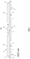
- Figure 1 shows a longitudinal sectional view of a capacitive voltage sensor 100 which can be integrated into a cable joint as from the present disclosure.
- the representation of Figure 1 is schematic and not necessarily in the correct scale.
- Figure 2a and 2b show possible bottom view and a top view, respectively, of the capacitive voltage sensor 100 of Figure 1 .
- the capacitive voltage sensor 100 comprises a sensor insulating layer 1, defining a first side 2 and an opposite second side 3.
- a sensor electrode 4 is placed on the second side 3 of the sensor insulating layer 1. In the present embodiment, the sensor electrode 4 covers only a portion of the surface of the second side 3.
- the capacitive voltage sensor 100 also comprises one guard electrode 5 placed on the second side 3 of the sensor insulating layer 1.
- the guard electrode 5 of the present embodiment has a closed ring form and is laid on the second side 3 so as to circumscribe the sensor electrode 4.
- the guard electrode 5 is electrically isolated from the sensor electrode 4.
- the guard electrode 5 is spatially separated from the sensor electrode 4 (as in the present case) and/or an interposed insulating material ensures the reciprocal electrical isolation.
- the sensor electrode 4 and the guard electrode 5 are flexible and have, particularly, planar shapes.
- the capacitive voltage sensor 100 is provided with a sensor conductive layer 6 placed on the first side 2.
- the sensor conductive layer 6 can have the function of screen layer for shielding the sensor electrode 4 and the guard electrodes 5 from external noise.
- the conductive layer 6 is flexible and has, in particular, a planar shape.
- the sensor conductive layer 6 covers the majority of the first side 2 of the sensor insulating layer 1, for example the conductive layer 6 covers a percentage of the area of the sensor insulating layer 1 greater than 60%, more preferably greater than 80%.
- the sensor conductive layer 6 includes a first conductive layer portion 13 and a second conductive layer portion 14.
- the first conductive layer portion 13 is at least partially faced toward the guard electrode 5 and the second conductive layer portion 14 is at least partially faced toward the sensor electrode 4.
- the first conductive layer portion 13 is electrical isolated from the second conductive layer portion 14.
- the first conductive layer portion 13 is spatially separated from the second conductive layer portion 14 and/or an interposed insulating material ensures the reciprocal electrical isolation.
- the first conductive layer portion 13 and the second conductive layer portion 14 further to the above mentioned shielding function play also the roles of electrical contacts with a signal cable.
- the sensor insulating layer 1 includes a first contacting element 7 ( Figure 1 ) and second contacting elements 8 ( Figures 2a and 2b ) extending in holes formed through the sensor insulating layer 1.
- the first contacting element 7 connects the sensor electrode 4 with the second conductive layer portion 14, and the second contacting elements 8 connect the guard electrode 5 with the first conductive layer portion 13 of the conductive layer 6.
- the capacitive voltage sensor 100 is manufactured according to the Flexible Printed Circuit (FPC) Technology.
- the sensor insulating layer 1 can be made in one of the following materials: a polyester, such as PET or PEN, or a polyimide, such as poly (4,4'-oxydiphenylene-pyromellitimide) (marketed as KaptonTM by DuPont).
- the guard electrode 5 and the sensor electrode 4 can be in form of copper foil, optionally finished by tin, silver foil, carbon foil, carbon nano-tube foil, gold foil or a conductive polymer layer, or in form of an ink or a paint.
- the conductive material forming the first contacting element 7 and the second contacting elements 8 can be copper, aluminium, carbon, conductive polymer.
- the sensor conductive layer 6 is made, as an example, in one of the materials listed for the sensor electrode 4 and the guard electrode 5. Particularly, it is observed that the material of the sensor insulating layer 1 may at least partially fill gap zones 19 between the sensor electrode 4 and the guard electrode 5 and, as an example, between the first conductive layer portion 13 and the second conductive layer portion 14 ( Figure 1 ).
- the capacitive voltage sensor 100 of Figures 1 and 2a-2c has, as an example, a parallelepiped body where the sensor electrode 4 (having, in this case, a quadrangular shape) is placed in a central area of the second side 3, and the guard electrode 5 has a quadrangular shape surrounding the sensor electrode 4.
- the capacitive voltage sensor 100 may have different shapes, for example, rectangular or circular shape, and the sensor electrode 4, the guard electrode 5, the first conductive layer portion 13 and/or the second conductive layer portion 14 may vary in shape accordingly.
- Figure 2c shows a portion of the capacitive voltage sensor 100. According to the shown example, this portion includes ends of a signal cable employed to provide a sensor signal outside the capacitive voltage sensor 100.
- the capacitive voltage sensor 100 is connectable with a signal cable 400 (shown in Figures 4-7 ) comprising a first wire end 17, connected to the first conductive layer portion 13 of the sensor conductive layer 6 to carry a reference signal, and a second wire end 15, connected to the second conductive layer portion 14 to carry a sensor signal.
- the signal cable 400 is a twisted pair cable comprising the first wire end 17 and the second wire end 15.
- the capacitive voltage sensor 100 may be connected with a redundant signal cable comprising a third wire end 16 connected to the second conductive layer portion 14 to carry the guard signal, and a fourth wire end 20 connected to the first conductive layer portion 13 to carry the sensor signal.
- the capacitive voltage sensor 100 is manufactured according to the FPC technology; the sensor insulating layer 1, made of KaptonTM, has a thickness of 35 ⁇ m; and the capacitive voltage sensor 100 has a side length L of 50 mm.
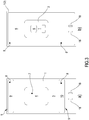
- FIGs 3a and 3b show another embodiment of the capacitive voltage sensor 100 according to the present disclosure.
- the capacitive voltage sensor 100 has a parallelepiped shape and the guard electrode 5 is divided into two portions, a first portion 9 and a separated second portion 10 which are, in the present case, substantially equidistant from the sensor electrode 4.
- the sensor conductive layer 6 and the second connecting elements 8 electrically connect the first portion 9 with the second portion 10 of the guard electrode 5.
- the sensor comprises holes 18 that allows connection to the signal cable 400.
- Figures 4-7 refer to sectional views of a joint 200, which can be a cold shrinkable joint.
- the joint 200 shown in Figure 4-7 is installed over a metallic connector 500 used to splice together two cable conductors 300, 302.
- the joint 200 can be employed in medium voltage power distribution systems.
- the metallic connector 500 can be a known shear bolt connector (provided with an aluminium foil) which connects a first cable conductor 300 of a first cable end 301 with a second cable conductor 302 of a second cable end 303.
- the two jointed cables are single-core medium-voltage cables.
- Each of the first 301 and second cable end 303 includes a cable insulation layer 304, surrounding the first cable conductor 300 and second cable conductor 302, respectively.
- Each of the first 301 and the second cable end 303 is provided with a cable semiconductive layer 305.
- Each of the first 301 and the second cable end 303 further includes a cable screen 306 laying on a corresponding cable sheath 307, as result of the installation procedure ( Figures 4 and 7 ).
- the cable screen 306 can be made of wires, helically wound tapes or a longitudinally folded foil.
- the cable screen material can be copper, aluminium, lead or a composite thereof.
- the joint 200 has a substantially cylindrical shape and comprises a central portion 201 and two end portions 202 connected to a respective end of the central portion 201.
- the joint 200 is made by a plurality of coaxial layers having substantially tubular shapes.
- the joint 200 comprises (from the outside to the inside) a joint sheath 203, a joint screen layer 204 (made, for example, in the form of a metal braid), a joint semiconductive layer 206 and a joint insulating layer 211 and, in this embodiment, a high permittivity layer 212 and a high permittivity mastic structure 213.
- the joint insulating layer 211 surrounds a connection region configured to house metallic connector 500.
- the joint sheath 203 can be made of an elastomeric material, such as ethylene propylene rubber (EPR), ethylene propylene diene monomer rubber (EPDM), silicone rubber, butyl rubber.
- EPR ethylene propylene rubber
- EPDM ethylene propylene diene monomer rubber
- silicone rubber butyl rubber.
- the joint insulating layer 211 can be made, as an example of: EPR, EPDM, silicone rubber; butyl rubber.
- the joint semiconductive layer 206 can be made in the same material of the joint insulating layer 211 and include, in addition, a conductive filler (such as, carbon black) so as to reach the required conductivity, e.g. a conductivity comprised between 10 -1 and 10 S/m.
- a conductive filler such as, carbon black
- the joint sheath 203, the joint screen layer 204 and the joint semiconductive layer 206 extends from the central portion 201 to the two end portions 202.
- the central portion 201 and the two end portions 202 show an elastic behaviour.
- the materials used for manufacturing the joint 200 are of the type that allow the joint 200 to perform a cold shrink over the interconnected cable ends.
- the joint 200 comprises a capacitive voltage sensor 100 and a signal cable 400 (e.g. a coaxial cable).
- the capacitive voltage sensor 100 is arranged between the joint screen layer 204 and the joint semiconductive layer 206, and is kept in place by a semiconducting tape or elastic sleeve 210 provided in radial internal position with respect to the joint screen layer 204.
- the semiconducting tape 210 extends in the central region 201.
- An insulating filler 205 (in form, for example, of a tape) partially covers the capacitive voltage sensor 100 and is in radial internal position with respect to the semiconducting tape 210.
- the insulating filler is made in a material selected from: polyvinyl chloride (PVC); ethylene propylene rubber (EPR); ethylenepropylene diene monomer (EPDM); silicone rubber; butyl rubber.
- the insulating filler 205 may also provide for insulation of the first conductive layer portion 13 from the second conductive layer portion 14.
- the guard electrode 5 and the sensor electrode 4 are in direct contact with the joint semiconductive layer 206.
- the semiconductive layer 206 may at least partially fill the gap zone 19 ( Fig. 1 ), such as the gap between the sensor electrode 4 and the guard electrode 5.
- a portion of the sensor conductive layer 6 is in direct contact with an inner face of the semiconducting tape 210 and another portion of the sensor conductive layer 6 is in contact with the insulating filler 205.
- sensor conductive layer 6 fully contacts the semiconducting tape 210 on one side and cable screen 204 on the other side.
- the signal cable 400 extends from the capacitive voltage sensor 100 to one of joint end portions 202 where has an output port 410 ( Figures 4 and 7 ).
- the signal cable 400 of the embodiments of Figures 4-7 is a coaxial cable but, as already described, other types of cables can be used, such as twisted-pair cables or shielded flat cables.
- the signal coaxial cable 400 of Figures 4-7 comprises a core conductor 401, a dielectric insulator 402 and a conducting shield 403 ( Figure 6 ).
- the core conductor 401 is connected, e.g. via a soldering, to the second conductive layer portion 14 and the conducting shield 403 is connected to the first conductive layer portion 13 of the conductive layer 6.
- the output port 410 is configured to be connected to an external connector employed to transfer a detected voltage signal toward an external device.
- the signal coaxial cable 400 is also provided with a cable jacket 405 surrounding the conducting shield 403.
- an end of the conducting shield 403 is connected to the first conductive layer portion 13 to allow direct electrical contact (with or without the interposition of a soldering material) so avoiding the necessity an internal connection wire.
- joint 200 is made to collapse on the first 301 and second 303 cable ends, for example by a cold shrink action.
- joint 200 can be mounted in a manner analogous to the one employed for the cold-shrink cable splice Elaspeed® marketed by the Applicant.
- the sensor electrode 4 is arranged so as to be capacitively coupled with the metallic connector 500 to detect a voltage detected signal depending on an electrical voltage of the first 301 and second cable ends 303.
- the cable screen 306 of the first 301 and second cable ends 303, together with the screen layer 204 of the joint 200, are connected to a ground terminal GND ( Figure 4 ).
- the sensor electrode 4 and the guard electrode 5 are in direct contact with the joint semiconductive layer 206.
- the first conductive layer portion 13 is electrically connected to the joint screen layer 204, via the semiconducting tape 210 (which represents a low impedance link), and so the guard electrode 5 is electrically connected to the ground terminal GND.
- the guard electrode 5, connected to the ground terminal GND via a low impedance link, imparts ground potential to the region of the joint semiconductive layer 206 to which it is in contact.
- the conducting shield 403 of the signal coaxial cable 400 provides the ground voltage assumed by the guard electrode 5 to the output port 410; the ground voltage represents a reference signal for the measure of a voltage value associated with the voltage signal detected by the sensor electrode 4.
- the voltage signal conveyed outside the joint 200 can be measured by a voltmeter or another measuring device connected to the output port 410 and the measured voltage value depends on the voltage of the electrical current flowing in the cable connector 500.
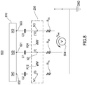
- Figure 8 shows an electrical circuit 600 equivalent to the components of the joint 200 involved in the voltage sensing. Particularly, the following description refers to the capacitive voltage sensor 100 of Figure 3 where the guard electrode 5 comprises a first portion 9 and a second portion 10, but it is valid in an analogous manner also for the embodiment of figure 1 and 2 .
- an electrical component 610 comprising the metallic connector 500, the first cable conductor 300 and the second cable conductor 302, is provided with a first terminal 601, a second terminal 602 and a third terminal 603.
- the first terminal 601 is connected to a first capacitive component C1 representing the capacitance of the portion of the joint insulating layer 211 comprised between the sensor electrode 4 and the metallic connector 500 ( Figure 5 ).
- the second terminal 602 is connected to a second capacitive component C2 representing the capacitance of the portion of the joint insulating layer 211 comprised between the first portion 9 of the guard electrode 5 and the metallic connector 500.
- the third terminal 603 is connected to a third capacitive component C3 representing the capacitance of the portion of the joint insulating layer 211 comprised between the second portion 10 of the guard electrode 5 and the metallic connector 500.
- a first resistor R 12 represents a resistance of a longitudinal portion of the joint semiconductive layer 206 faced to a region extending between the first portion 9 of the guard electrode 5 and the sensor electrode 4.
- a second resistor R 24 represents a resistance of another longitudinal portion of the joint semiconductive layer 206 faced to a further region extending between the sensor electrode 4 and the second portion 10 of the guard electrode 5.
- a third resistor R 1R , a fourth resistor R 2R and fifth resistor R 3R respectively represent the radial resistances of the portions of the joint semiconductive layer 206 in contact with the sensor electrode 4, the first portion 9 and second portion 10 of guard electrode 5.
- the second capacitive component C2 is connected between the second terminal 602 and a first node N1; the first capacitive component C1 is connected between the first terminal 601 and a second node N2, the third capacitive component C3 is connected between the third terminal 603 and a third node N3.
- the first resistor R 1L is connected between the first node N1 and the second node N2.
- the second resistor R 2L is connected between the second node N2 and the third node N3.
- the third resistor R 1R is connected between the first node N1 and the ground terminal GND.
- the fourth resistor R 2R is connected between the second node N2 and a measuring device 604 (such as a voltmeter) also connected with the ground terminal GND.
- the fifth resistor R 3R is connected between the third node N3 and the ground terminal GND.
- a voltage value V out measurable by the voltmeter 604 corresponds to the voltage drop on the second resistor R 2L .
- the measured voltage value V out it is possible to evaluate if the voltage signal value overcomes a voltage threshold to decide about the presence or absence of the applied voltage V in the cables jointed by the joint 200, without calculating a value of the applied voltage V.
- the capacitive voltage sensor of the present disclosure can be integrated in any kind of cable joints, in separable connectors or in power cables to measure applied voltage or partial discharge signals.
- the presence of the sensor conductive layer allows noise shielding of the electrodes.
- the conductive layer also provides for electrical connection (e.g. with the signal cable) simplifying the sensor structure and reducing or avoiding the number of internal wires.
- the capacitive voltage sensor of the disclosure can have a flexible structure that allows non-complex integration in cable joints and manufacturing of fully elastic cable joints.
- the joint encompassing the capacitive voltage sensor of the disclosure is provided with continuous screen layer and sheath so providing high safety performances, in accessing the sensor to read the detected voltage. Particularly, the presence of the uninterrupted joint sheath improves the impermeability of the joint.
- the joint of the present disclosure can be manufactured with an uninterrupted joint semiconductive layer so avoiding discontinuity (circular hole) in this layer.
- the joint of the disclosure operates on the basis a capacitance associated with its insulation and a resistance associated with its semiconductive layer which is part of the joint and is not dependent on external components.
Landscapes
- Physics & Mathematics (AREA)
- General Physics & Mathematics (AREA)
- Engineering & Computer Science (AREA)
- Microelectronics & Electronic Packaging (AREA)
- Measuring Instrument Details And Bridges, And Automatic Balancing Devices (AREA)
- Cable Accessories (AREA)
- Geophysics And Detection Of Objects (AREA)
Abstract
Description
- The present disclosure relates to voltage sensing tools employable, particularly, in shrinkable cable joints.
- Shrinkable joints, either cold or heat shrinkable, employed to connect high or medium voltage cables and provided with capacitive voltage test sockets comprising a metallic insert for detecting the presence of voltage in cable lines are known.
-
US2012/0273246 discloses a cold shrinkable primary joint of the type provided with a capacitive voltage socket. The joint described by this document comprises an electrically conductive rubber exterior, an electrically and thermally conductive insert, that serves as Faraday cage, and an insulating material disposed between the electrically and thermally conductive insert and the electrically conductive rubber exterior. Moreover, the joint is provided with a capacitive test point structure having a capacitive test point that extends down into the insulating material towards the insert and out beyond the electrically conductive rubber exterior. - With reference to capacitive voltage test sockets, the Applicant observes that the voltage output is, typically, of the order of magnitude of 1 kV so there are potential safety issues for the operator, also because for accessing a capacitive insert to collect the detected voltage the sensor accessory cannot be electrically screened and a fault current cannot be drained to ground through the joint semi-conductive material without increasing temperature and voltage. Moreover, as the sensor accessory comprises a rigid metal insert, it is not elastic and, especially, it cannot shrink to adapt to the joint modification in view of the cable size.
-
WO 2012/130816 relates to an apparatus for measuring the potential on a shielded high voltage cable. A capacitive sensor arrangement is constructed on a cable. The capacitive sensor includes a sensor comprising a sensing electrode positioned on the semiconducting layer of the cable, a dielectric layer and an electrostatic shield. The capacitive sensor includes a coaxial conductor that provides electrical connection to the sensing electrode, by a corresponding wire connection, and to the electrostatic shield by another wire connection. - The Applicant observed that the known shrinkable joints show drawbacks in terms of safety performances and elasticity of their structures. The Applicant further noted that voltage sensors showing compact and non-complex structures that facilitate integration in electrical components, such as shrinkable cable joints, are needed.
- The Applicant has found that a capacitive voltage sensor having an insulating layer having sensor and guard electrodes on a side and a conductive layer extending on the opposite side and electrically contacting both sensor and guard electrodes, is suitable to meet safety, elasticity and adjustability issues, with particular reference to the incorporation in shrinkable joints, either cold or heat shrinkable.
- According to a first aspect, the present disclosure relates to a shrinkable joint comprising:
- a joint insulating layer surrounding a connection region configured to house two electrically connected cable ends;
- a joint semiconductive layer surrounding the joint insulating layer;
- a joint screen layer surrounding the joint semiconductive layer;
- a joint sheath surrounding the joint screen layer; and
- a capacitive voltage sensor arranged between the joint screen layer and the joint semiconductive layer and comprising:
- a sensor insulating layer having a first side and an opposite second side;
- a sensor electrode and a guard electrode arranged on the second side and directly contacting the joint semiconductive layer;
- a sensor conductive layer arranged on the first side and comprising a first conductive layer portion in direct contact with the joint screen layer and electrically connected to the guard electrode; and a second conductive layer portion electrically connected to the sensor electrode; the conductive layer extending on the first side.
- In an embodiment, the capacitive voltage sensor has a planar structure being, for example, of one of the following shapes: rectangular shape, quadrangular shape, circular shape. In an embodiment, the capacitive voltage sensor is flexible.
- In an embodiment, the sensor electrode and guard electrode are flexible. In an embodiment, the sensor electrode and guard electrode have planar shapes.
- In an embodiment, the first conductive layer portion and the second conductive layer portion are flexible. In an embodiment, the first conductive layer portion and the second conductive layer portion have planar shapes.
- In an embodiment, the joint of the present disclosure further includes a sensor insulating layer arranged to electrically insulate the first conductive layer portion from the second conductive layer portion. For example, the sensor insulating layer is made of a material selected from: polyester; polyethylene terephthalate (PET); polyethylene naphthalate (PEN); polyimide.
- In an embodiment, the first conductive layer portion has a first area greater than a second area of the second conductive layer portion.
- For example, the sensor electrode, guard electrode and conductive layer are made of a material selected from: a metal like copper, tinned copper, silver, or gold; carbon, carbon nano-tube, a conductive polymer, or composites thereof.
- In an embodiment, the capacitive voltage sensor is made according to a Flexible Printed Circuit (FPC) Technology.
- In an embodiment, the sensor insulating layer comprises: a first conductive element connecting the guard electrode with first conductive layer portion and a second conductive element connecting the sensor electrode with the second conductive layer portion.
- In an embodiment, the joint of the present disclosure further comprises a signal cable comprising: a first conductor having a first end electrically connected to the second conductive layer portion and a second end connected to an output port; a second conductor having a respective third end electrically connected to the first conductive layer portion of the conductive layer and a respective fourth terminal connected to the output port. The signal cable can be one of the following cable types: coaxial cable, twisted-pair cable, shielded flat cable.
- For example, the sheath of the joint can be made of an elastomeric material selected from: ethylene propylene rubber (EPR); ethylene propylene diene monomer rubber (EPDM); silicone rubber, butyl rubber.
- In an embodiment, the capacitive voltage sensor is arranged in the joint of the present disclosure to detect a voltage signal dependent on:
- a capacitance value associated with the joint insulating layer;
- a first resistance value associated with a portion of the joint semiconductive layer faced to a longitudinal region extending between the sensor electrode and a first portion of the guard electrode; and
- a second resistance value associated with a further portion of the semiconductive outer layer faced to a further region extending between the sensor electrode and a second portion of the guard electrode, the sensor electrode being arranged between the first portion and the second portion.
- In accordance with another aspect, the present disclosure relates to a capacitive voltage sensor comprising:
- a sensor insulating layer having a first side and an opposite second side;
- a sensor electrode and a guard electrode arranged on the second side;
- a sensor conductive layer arranged on the first side and comprising a first conductive layer portion electrically connected to the guard electrode a second conductive layer portion electrically connected to the sensor electrode; the conductive layer extending on the first side.
- a joint insulating layer surrounding a connection region configured to house the spliced cable conductors;
- a joint semiconductive layer surrounding the joint insulating layer;
- a joint screen layer surrounding the joint semiconductive layer;
- a joint sheath surrounding the joint screen layer; and
- a capacitive voltage sensor arranged between the joint screen layer and said joint semiconductive layer and comprising:
- a sensor insulating layer having a first side and an opposite second side;
- a sensor electrode and a guard electrode arranged on said second side and directly contacting the joint semiconductive layer;
- a sensor conductive layer arranged on said first side and comprising a first conductive layer portion in direct contact with the joint screen layer and electrically connected to the guard electrode and a second conductive layer portion electrically connected to the sensor electrode; the sensor conductive layer extending on the first side.
- Further characteristics and advantages will be more apparent from the following description of a preferred embodiment and of its alternatives given as a way of an example with reference to the enclosed drawings in which:
-
Figure 1 shows, schematically, a longitudinal sectional view of a capacitive voltage sensor according to an embodiment of the present disclosure; -
Figures 2a, 2b, 2c show the capacitive voltage sensor ofFigure 1 in a bottom view (Figure 2a ), top view (Figure 2b ) and further details of the top view (Figure 2c ); -
Figures 3a and 3b show, respectively, a bottom view and a top view of another embodiment of the capacitive voltage sensor of the disclosure; -
Figure 4 shows a longitudinal sectional view of an embodiment of a joint according to the present disclosure comprising a capacitive voltage sensor; -
Figure 5 shows a longitudinal sectional view of a centre portion of the joint ofFigure 4 ; -
Figure 6 shows, in a longitudinal sectional view, a side portion of the joint ofFigure 4 ; -
Figure 7 shows, in a longitudinal sectional view, another side portion of the joint ofFigure 4 ; -
Figure 8 shows an equivalent electrical circuit illustrating the operation of the voltage sensor of the present disclosure. - For the purpose of the present description and of the appended claims, except where otherwise indicated, all numbers expressing amounts, quantities, percentages, and so forth, are to be understood as being modified in all instances by the term "about". Also, all ranges include any combination of the maximum and minimum points disclosed and include any intermediate ranges therein, which may or may not be specifically enumerated herein.
- As used in the present description and the appended claims, the singular forms "a," "an," and "the" include plural referents unless the context clearly dictates otherwise. In this specification and in the claims that follow, reference will be made to a number of terms that shall be defined to have the following meanings unless a contrary intention is apparent.
- For the purpose of the present description and of the appended claims, the term "conductive" and "semiconductive" are construed to mean "electrically conductive" and "electrically semiconductive".
- In the following description, same alphanumeric references are used for analogous exemplary elements when they are depicted in different drawings.
-
Figure 1 shows a longitudinal sectional view of acapacitive voltage sensor 100 which can be integrated into a cable joint as from the present disclosure. The representation ofFigure 1 is schematic and not necessarily in the correct scale.Figure 2a and 2b show possible bottom view and a top view, respectively, of thecapacitive voltage sensor 100 ofFigure 1 . - The
capacitive voltage sensor 100 comprises asensor insulating layer 1, defining afirst side 2 and an oppositesecond side 3. Asensor electrode 4 is placed on thesecond side 3 of thesensor insulating layer 1. In the present embodiment, thesensor electrode 4 covers only a portion of the surface of thesecond side 3. - The
capacitive voltage sensor 100 also comprises oneguard electrode 5 placed on thesecond side 3 of thesensor insulating layer 1. As fromFigure 2a , theguard electrode 5 of the present embodiment has a closed ring form and is laid on thesecond side 3 so as to circumscribe thesensor electrode 4. Theguard electrode 5 is electrically isolated from thesensor electrode 4. As an example, theguard electrode 5 is spatially separated from the sensor electrode 4 (as in the present case) and/or an interposed insulating material ensures the reciprocal electrical isolation. For example, thesensor electrode 4 and theguard electrode 5 are flexible and have, particularly, planar shapes. - The
capacitive voltage sensor 100 is provided with a sensorconductive layer 6 placed on thefirst side 2. The sensorconductive layer 6 can have the function of screen layer for shielding thesensor electrode 4 and theguard electrodes 5 from external noise. In an example, theconductive layer 6 is flexible and has, in particular, a planar shape. - In the present embodiment, the sensor
conductive layer 6 covers the majority of thefirst side 2 of thesensor insulating layer 1, for example theconductive layer 6 covers a percentage of the area of thesensor insulating layer 1 greater than 60%, more preferably greater than 80%. - The sensor
conductive layer 6 includes a firstconductive layer portion 13 and a secondconductive layer portion 14. The firstconductive layer portion 13 is at least partially faced toward theguard electrode 5 and the secondconductive layer portion 14 is at least partially faced toward thesensor electrode 4. The firstconductive layer portion 13 is electrical isolated from the secondconductive layer portion 14. As an example, the firstconductive layer portion 13 is spatially separated from the secondconductive layer portion 14 and/or an interposed insulating material ensures the reciprocal electrical isolation. As will be described in detail hereinafter, the firstconductive layer portion 13 and the secondconductive layer portion 14 further to the above mentioned shielding function play also the roles of electrical contacts with a signal cable. - The
sensor insulating layer 1 includes a first contacting element 7 (Figure 1 ) and second contacting elements 8 (Figures 2a and 2b ) extending in holes formed through thesensor insulating layer 1. The first contactingelement 7 connects thesensor electrode 4 with the secondconductive layer portion 14, and the second contactingelements 8 connect theguard electrode 5 with the firstconductive layer portion 13 of theconductive layer 6. - In an embodiment of the present disclosure, the
capacitive voltage sensor 100 is manufactured according to the Flexible Printed Circuit (FPC) Technology. Thesensor insulating layer 1 can be made in one of the following materials: a polyester, such as PET or PEN, or a polyimide, such as poly (4,4'-oxydiphenylene-pyromellitimide) (marketed as Kapton™ by DuPont). Theguard electrode 5 and thesensor electrode 4 can be in form of copper foil, optionally finished by tin, silver foil, carbon foil, carbon nano-tube foil, gold foil or a conductive polymer layer, or in form of an ink or a paint. - The conductive material forming the first contacting
element 7 and the second contactingelements 8 can be copper, aluminium, carbon, conductive polymer. The sensorconductive layer 6 is made, as an example, in one of the materials listed for thesensor electrode 4 and theguard electrode 5. Particularly, it is observed that the material of thesensor insulating layer 1 may at least partially fillgap zones 19 between thesensor electrode 4 and theguard electrode 5 and, as an example, between the firstconductive layer portion 13 and the second conductive layer portion 14 (Figure 1 ). - The
capacitive voltage sensor 100 ofFigures 1 and2a-2c has, as an example, a parallelepiped body where the sensor electrode 4 (having, in this case, a quadrangular shape) is placed in a central area of thesecond side 3, and theguard electrode 5 has a quadrangular shape surrounding thesensor electrode 4. In alternative embodiments, thecapacitive voltage sensor 100 may have different shapes, for example, rectangular or circular shape, and thesensor electrode 4, theguard electrode 5, the firstconductive layer portion 13 and/or the secondconductive layer portion 14 may vary in shape accordingly. -
Figure 2c shows a portion of thecapacitive voltage sensor 100. According to the shown example, this portion includes ends of a signal cable employed to provide a sensor signal outside thecapacitive voltage sensor 100. - According to the particular example of
Figures 2a-2c , thecapacitive voltage sensor 100 is connectable with a signal cable 400 (shown inFigures 4-7 ) comprising afirst wire end 17, connected to the firstconductive layer portion 13 of the sensorconductive layer 6 to carry a reference signal, and asecond wire end 15, connected to the secondconductive layer portion 14 to carry a sensor signal. As an example, thesignal cable 400 is a twisted pair cable comprising thefirst wire end 17 and thesecond wire end 15. Thecapacitive voltage sensor 100 may be connected with a redundant signal cable comprising athird wire end 16 connected to the secondconductive layer portion 14 to carry the guard signal, and afourth wire end 20 connected to the firstconductive layer portion 13 to carry the sensor signal. - In the embodiment of
Figures 2a-2c , thecapacitive voltage sensor 100 is manufactured according to the FPC technology; thesensor insulating layer 1, made of Kapton™, has a thickness of 35 µm; and thecapacitive voltage sensor 100 has a side length L of 50 mm. -
Figures 3a and 3b show another embodiment of thecapacitive voltage sensor 100 according to the present disclosure. In this embodiment, thecapacitive voltage sensor 100 has a parallelepiped shape and theguard electrode 5 is divided into two portions, afirst portion 9 and a separatedsecond portion 10 which are, in the present case, substantially equidistant from thesensor electrode 4. As fromFigure 3b , the sensorconductive layer 6 and the second connectingelements 8 electrically connect thefirst portion 9 with thesecond portion 10 of theguard electrode 5. As shown inFigure 3b the sensor comprisesholes 18 that allows connection to thesignal cable 400. -
Figures 4-7 refer to sectional views of a joint 200, which can be a cold shrinkable joint. The joint 200 shown inFigure 4-7 is installed over ametallic connector 500 used to splice together twocable conductors - The
metallic connector 500 can be a known shear bolt connector (provided with an aluminium foil) which connects afirst cable conductor 300 of afirst cable end 301 with asecond cable conductor 302 of asecond cable end 303. According to an example, the two jointed cables are single-core medium-voltage cables. - Each of the first 301 and
second cable end 303 includes acable insulation layer 304, surrounding thefirst cable conductor 300 andsecond cable conductor 302, respectively. - Each of the first 301 and the
second cable end 303 is provided with acable semiconductive layer 305. Each of the first 301 and thesecond cable end 303 further includes acable screen 306 laying on acorresponding cable sheath 307, as result of the installation procedure (Figures 4 and7 ). Thecable screen 306 can be made of wires, helically wound tapes or a longitudinally folded foil. The cable screen material can be copper, aluminium, lead or a composite thereof. - The joint 200 has a substantially cylindrical shape and comprises a
central portion 201 and twoend portions 202 connected to a respective end of thecentral portion 201. The joint 200 is made by a plurality of coaxial layers having substantially tubular shapes. In particular and with reference toFigure 5 , the joint 200 comprises (from the outside to the inside) ajoint sheath 203, a joint screen layer 204 (made, for example, in the form of a metal braid), a jointsemiconductive layer 206 and a joint insulatinglayer 211 and, in this embodiment, ahigh permittivity layer 212 and a highpermittivity mastic structure 213. The joint insulatinglayer 211 surrounds a connection region configured to housemetallic connector 500. - The
joint sheath 203 can be made of an elastomeric material, such as ethylene propylene rubber (EPR), ethylene propylene diene monomer rubber (EPDM), silicone rubber, butyl rubber. The joint insulatinglayer 211 can be made, as an example of: EPR, EPDM, silicone rubber; butyl rubber. - The joint
semiconductive layer 206 can be made in the same material of the joint insulatinglayer 211 and include, in addition, a conductive filler (such as, carbon black) so as to reach the required conductivity, e.g. a conductivity comprised between 10-1 and 10 S/m. - The
joint sheath 203, thejoint screen layer 204 and the jointsemiconductive layer 206 extends from thecentral portion 201 to the twoend portions 202. Thecentral portion 201 and the twoend portions 202 show an elastic behaviour. - It is noticed that the materials used for manufacturing the joint 200 are of the type that allow the joint 200 to perform a cold shrink over the interconnected cable ends.
- The joint 200 comprises a
capacitive voltage sensor 100 and a signal cable 400 (e.g. a coaxial cable). Thecapacitive voltage sensor 100 is arranged between thejoint screen layer 204 and the jointsemiconductive layer 206, and is kept in place by a semiconducting tape orelastic sleeve 210 provided in radial internal position with respect to thejoint screen layer 204. Thesemiconducting tape 210 extends in thecentral region 201. - An insulating filler 205 (in form, for example, of a tape) partially covers the
capacitive voltage sensor 100 and is in radial internal position with respect to thesemiconducting tape 210. For example, the insulating filler is made in a material selected from: polyvinyl chloride (PVC); ethylene propylene rubber (EPR); ethylenepropylene diene monomer (EPDM); silicone rubber; butyl rubber. - As the
capacitive voltage sensor 100 is positioned in the joint 200 so that thefirst side 2 is radially external to thesecond side 3, in an embodiment the insulatingfiller 205 may also provide for insulation of the firstconductive layer portion 13 from the secondconductive layer portion 14. - The
guard electrode 5 and thesensor electrode 4 are in direct contact with the jointsemiconductive layer 206. As an example, thesemiconductive layer 206 may at least partially fill the gap zone 19 (Fig. 1 ), such as the gap between thesensor electrode 4 and theguard electrode 5. According to the example shown, a portion of the sensorconductive layer 6 is in direct contact with an inner face of thesemiconducting tape 210 and another portion of the sensorconductive layer 6 is in contact with the insulatingfiller 205. In another, not illustrated embodiment, sensorconductive layer 6 fully contacts thesemiconducting tape 210 on one side andcable screen 204 on the other side. - The
signal cable 400 extends from thecapacitive voltage sensor 100 to one ofjoint end portions 202 where has an output port 410 (Figures 4 and7 ). Thesignal cable 400 of the embodiments ofFigures 4-7 is a coaxial cable but, as already described, other types of cables can be used, such as twisted-pair cables or shielded flat cables. - The signal
coaxial cable 400 ofFigures 4-7 comprises acore conductor 401, adielectric insulator 402 and a conducting shield 403 (Figure 6 ). Thecore conductor 401 is connected, e.g. via a soldering, to the secondconductive layer portion 14 and the conductingshield 403 is connected to the firstconductive layer portion 13 of theconductive layer 6. Theoutput port 410 is configured to be connected to an external connector employed to transfer a detected voltage signal toward an external device. - The signal
coaxial cable 400 is also provided with acable jacket 405 surrounding the conductingshield 403. In an embodiment, an end of the conductingshield 403 is connected to the firstconductive layer portion 13 to allow direct electrical contact (with or without the interposition of a soldering material) so avoiding the necessity an internal connection wire. - Once positioned onto the
metallic connector 500, as known to the skilled person, the joint 200 is made to collapse on the first 301 and second 303 cable ends, for example by a cold shrink action. As an example, joint 200 can be mounted in a manner analogous to the one employed for the cold-shrink cable splice Elaspeed® marketed by the Applicant. Thesensor electrode 4 is arranged so as to be capacitively coupled with themetallic connector 500 to detect a voltage detected signal depending on an electrical voltage of the first 301 and second cable ends 303. - It is observed that the presence of the
capacitive voltage sensor 100 encompassed in the joint 200 does not make more complex the joint installation steps. - In operation, the
cable screen 306 of the first 301 and second cable ends 303, together with thescreen layer 204 of the joint 200, are connected to a ground terminal GND (Figure 4 ). As fromFigure 5 , in thecapacitive voltage sensor 100, thesensor electrode 4 and theguard electrode 5 are in direct contact with the jointsemiconductive layer 206. The firstconductive layer portion 13 is electrically connected to thejoint screen layer 204, via the semiconducting tape 210 (which represents a low impedance link), and so theguard electrode 5 is electrically connected to the ground terminal GND. Theguard electrode 5, connected to the ground terminal GND via a low impedance link, imparts ground potential to the region of the jointsemiconductive layer 206 to which it is in contact. - If there is a non-zero electric AC voltage along the cables jointed by the
metallic connector 500, an electrical current is induced by capacitive coupling in the jointsemiconductive layer 206. Therefore, this capacitive current passes through the jointsemiconductive layer 206 to flow up to the ground terminal GND causing a voltage drop in the jointsemiconductive layer 206. Thesensor electrode 4 and the secondconductive layer portion 14 harvest such voltage drop and transmit a corresponding voltage signal to thecore conductor 401 of the signalcoaxial cable 400 so this voltage signal can be conveyed outside the joint 200 via theoutput port 410. Moreover, the conductingshield 403 of the signalcoaxial cable 400 provides the ground voltage assumed by theguard electrode 5 to theoutput port 410; the ground voltage represents a reference signal for the measure of a voltage value associated with the voltage signal detected by thesensor electrode 4. The voltage signal conveyed outside the joint 200 can be measured by a voltmeter or another measuring device connected to theoutput port 410 and the measured voltage value depends on the voltage of the electrical current flowing in thecable connector 500. -
Figure 8 shows anelectrical circuit 600 equivalent to the components of the joint 200 involved in the voltage sensing. Particularly, the following description refers to thecapacitive voltage sensor 100 ofFigure 3 where theguard electrode 5 comprises afirst portion 9 and asecond portion 10, but it is valid in an analogous manner also for the embodiment offigure 1 and2 . - In the equivalent circuit of
Figure 8 anelectrical component 610, comprising themetallic connector 500, thefirst cable conductor 300 and thesecond cable conductor 302, is provided with afirst terminal 601, asecond terminal 602 and athird terminal 603. Thefirst terminal 601 is connected to a first capacitive component C1 representing the capacitance of the portion of the joint insulatinglayer 211 comprised between thesensor electrode 4 and the metallic connector 500 (Figure 5 ). Thesecond terminal 602 is connected to a second capacitive component C2 representing the capacitance of the portion of the joint insulatinglayer 211 comprised between thefirst portion 9 of theguard electrode 5 and themetallic connector 500. Thethird terminal 603 is connected to a third capacitive component C3 representing the capacitance of the portion of the joint insulatinglayer 211 comprised between thesecond portion 10 of theguard electrode 5 and themetallic connector 500. - A first resistor R12 represents a resistance of a longitudinal portion of the joint
semiconductive layer 206 faced to a region extending between thefirst portion 9 of theguard electrode 5 and thesensor electrode 4. A second resistor R24 represents a resistance of another longitudinal portion of the jointsemiconductive layer 206 faced to a further region extending between thesensor electrode 4 and thesecond portion 10 of theguard electrode 5. - A third resistor R1R, a fourth resistor R2R and fifth resistor R3R respectively represent the radial resistances of the portions of the joint
semiconductive layer 206 in contact with thesensor electrode 4, thefirst portion 9 andsecond portion 10 ofguard electrode 5. - Particularly, the second capacitive component C2 is connected between the
second terminal 602 and a first node N1; the first capacitive component C1 is connected between thefirst terminal 601 and a second node N2, the third capacitive component C3 is connected between thethird terminal 603 and a third node N3. The first resistor R1L is connected between the first node N1 and the second node N2. The second resistor R2L is connected between the second node N2 and the third node N3. The third resistor R1R is connected between the first node N1 and the ground terminal GND. The fourth resistor R2R is connected between the second node N2 and a measuring device 604 (such as a voltmeter) also connected with the ground terminal GND. The fifth resistor R3R is connected between the third node N3 and the ground terminal GND. - Considering as negligible the resistances of the fourth resistor R2R, of the third resistor R1R and of the fifth resistor R3R with respect to the internal resistance of the
voltmeter 604, a voltage value Vout measurable by thevoltmeter 604 corresponds to the voltage drop on the second resistor R2L. The voltage value Vout con be expressed as:
- IC1 is the capacitive current flowing through the first capacitive component C1;
- Rpar is the parallel of the first resistor R1L and the second resistor R2L;
- V is the voltage applied to the
metallic connector 500, thefirst conductor 300 andsecond conductor 302 with respect to ground GND; - f is the frequency of voltage V.
- According to another embodiment, from the measured voltage value Vout it is possible to evaluate if the voltage signal value overcomes a voltage threshold to decide about the presence or absence of the applied voltage V in the cables jointed by the joint 200, without calculating a value of the applied voltage V.
- The capacitive voltage sensor of the present disclosure can be integrated in any kind of cable joints, in separable connectors or in power cables to measure applied voltage or partial discharge signals.
- It is noticed that the capacitive voltage sensor of the present disclosure and the joint incorporating it show advantages over the known devices.
- The presence of the sensor conductive layer allows noise shielding of the electrodes. The conductive layer also provides for electrical connection (e.g. with the signal cable) simplifying the sensor structure and reducing or avoiding the number of internal wires.
- The capacitive voltage sensor of the disclosure can have a flexible structure that allows non-complex integration in cable joints and manufacturing of fully elastic cable joints.
- The joint encompassing the capacitive voltage sensor of the disclosure is provided with continuous screen layer and sheath so providing high safety performances, in accessing the sensor to read the detected voltage. Particularly, the presence of the uninterrupted joint sheath improves the impermeability of the joint.
- Contrary to the known joints having a metallic insert, the joint of the present disclosure can be manufactured with an uninterrupted joint semiconductive layer so avoiding discontinuity (circular hole) in this layer. Moreover, as discussed with reference to the equivalent circuit of
Figure 8 , the joint of the disclosure operates on the basis a capacitance associated with its insulation and a resistance associated with its semiconductive layer which is part of the joint and is not dependent on external components.

By measuring the resistance Rpar prior to the detection and knowing the parameters f and C1 (the latter depends only on the geometry of the joint 200 and on the material used for the joint insulating layer 211) it is possible to calculate the applied voltage V from the measured voltage Vout.
Claims (14)
- A shrinkable cable joint (200) comprising:a joint insulating layer (211) surrounding a connection region configured to house two connected cable ends;a joint semiconductive layer (206) surrounding the joint insulating layer (211);a joint screen layer (204) surrounding the joint semiconductive layer (206);a joint sheath (203) surrounding the joint screen layer (204); anda capacitive voltage sensor (100) arranged between the joint screen layer (204) and said joint semiconductive layer (206) and comprising:a sensor insulating layer (1) having a first side (2) and an opposite second side (3);a sensor electrode (4) and a guard electrode (5) arranged on said second side (3) and directly contacting the joint semiconductive layer (206);a sensor conductive layer (6) arranged on said first side (2) and comprising a first conductive layer portion (13) in direct contact with the joint screen layer (204) and electrically connected to the guard electrode (5) and a second conductive layer portion (14) electrically connected to the sensor electrode (4); the sensor conductive layer (6) extending on the first side (2).
- The joint of claim 1, wherein: the capacitive voltage sensor (100) has a planar structure and a shape selected from: rectangular shape, quadrangular shape, circular shape.
- The joint of claim 1, wherein the capacitive voltage sensor is flexible.
- The joint of claim 1 further including an insulating filler (205) arranged to electrically insulate the first conductive layer portion (13) from the second conductive layer portion (14).
- The joint of claim 1, wherein the first conductive layer portion (13) has a first area greater than a second area of the second conductive layer portion (14).
- The joint of claim 1, wherein said sensor electrode (4), guard electrode (5) and conductive layer (6) are made a material selected from: metal, carbon, carbon nano-tube, a conductive polymer or composites thereof.
- The joint of claim 1, wherein the sensor insulating layer (1) is made in a material selected from: polyester; polyethylene terephthalate; polyethylene naphthalate; polyimide.
- The joint of claim 1, wherein the capacitive voltage sensor (100) is made according to a Flexible Printed Circuit, FPC, Technology.
- The joint (200) of claim 1, wherein said sensor insulating layer (1) comprises:a first conductive element (8) connecting the guard electrode (5) with the first conductive layer portion (13), anda second conductive element (7) connecting the sensor electrode (5) with the second conductive layer portion (14).
- The joint (200) of claim 1, further comprising a signal cable (400) comprising:a first conductor (401) having a first end connected to the second conductive layer portion (14) and a second end connected to an output port (410);a second conductor (403) having a third end connected to the first conductive layer portion (13) of the sensor conductive layer (6) and a fourth terminal connected to the output port (410).
- The joint (200) of claim 11, wherein said signal cable (400) is one of the following cable types: coaxial cable (400), twisted-pair cable, shielded flat cable.
- The joint (200) of claim 1, wherein the capacitive voltage sensor (100) is arranged so as to detect a voltage signal (Vout) dependent on:a capacitance value (C1) associated with the joint insulating layer (211);a first resistance value (R12) associated with a portion of the joint semiconductive layer (206) faced to a longitudinal region extending between the sensor electrode (4) and a first portion (9) of the guard electrode (5); anda second resistance value (R24) associated with a further portion of the semiconductive outer layer (206) faced to a further region extending between the sensor electrode (4) and a second portion (10) of the guard electrode (5), the sensor electrode (4) being arranged between the first portion (9) and the second portion (10).
- A capacitive voltage sensor (100) comprising:a sensor insulating layer (1) having a first side (2) and an opposite second side (3);a sensor electrode (4) and a guard electrode (5) arranged on said second side (3) configured to perform a capacitive coupling with an electrical conductor (500);a sensor conductive layer (6) arranged on said first side (2) and comprising a first conductive layer portion (13) electrically connected to the guard electrode (5) a second conductive layer portion (14) electrically connected to the sensor electrode (4); the conductive layer (6) extending on the first side (2).
- Power distribution system comprising two cable conductors (300, 302) spliced in a shrinkable cable joint (200) comprising:a joint insulating layer (211) surrounding a connection region configured to house the spliced cable conductors (300, 302);a joint semiconductive layer (206) surrounding the joint insulating layer (211);a joint screen layer (204) surrounding the joint semiconductive layer (206);a joint sheath (203) surrounding the joint screen layer (204); anda capacitive voltage sensor (100) arranged between the joint screen layer (204) and said joint semiconductive layer (206) and comprising:a sensor insulating layer (1) having a first side (2) and an opposite second side (3);a sensor electrode (4) and a guard electrode (5) arranged on said second side (3) and directly contacting the joint semiconductive layer (206);a sensor conductive layer (6) arranged on said first side (2) and comprising a first conductive layer portion (13) in direct contact with the joint screen layer (204) and electrically connected to the guard electrode (5) and a second conductive layer portion (14) electrically connected to the sensor electrode (4); the sensor conductive layer (6) extending on the first side (2).
Priority Applications (7)
| Application Number | Priority Date | Filing Date | Title |
|---|---|---|---|
| ES18306422T ES2949965T3 (en) | 2018-10-30 | 2018-10-30 | Retractable cable joint and voltage sensor |
| EP18306422.9A EP3647796B1 (en) | 2018-10-30 | 2018-10-30 | Shrinkable cable joint and voltage sensor |
| AU2019250187A AU2019250187B2 (en) | 2018-10-30 | 2019-10-17 | Shrinkable cable joint and voltage sensor |
| CA3059570A CA3059570A1 (en) | 2018-10-30 | 2019-10-22 | Shrinkable cable joint and voltage sensor |
| BR102019022563-7A BR102019022563B1 (en) | 2018-10-30 | 2019-10-28 | RETRACTABLE CABLE JOINT, CAPACITIVE VOLTAGE SENSOR, AND, POWER DISTRIBUTION SYSTEM |
| US16/667,078 US10753962B2 (en) | 2018-10-30 | 2019-10-29 | Shrinkable cable joint and voltage sensor |
| CN201911040779.9A CN111122916B (en) | 2018-10-30 | 2019-10-30 | Retractable cable gland and voltage sensor |
Applications Claiming Priority (1)
| Application Number | Priority Date | Filing Date | Title |
|---|---|---|---|
| EP18306422.9A EP3647796B1 (en) | 2018-10-30 | 2018-10-30 | Shrinkable cable joint and voltage sensor |
Publications (3)
| Publication Number | Publication Date |
|---|---|
| EP3647796A1 true EP3647796A1 (en) | 2020-05-06 |
| EP3647796B1 EP3647796B1 (en) | 2023-06-07 |
| EP3647796C0 EP3647796C0 (en) | 2023-06-07 |
Family
ID=64267753
Family Applications (1)
| Application Number | Title | Priority Date | Filing Date |
|---|---|---|---|
| EP18306422.9A Active EP3647796B1 (en) | 2018-10-30 | 2018-10-30 | Shrinkable cable joint and voltage sensor |
Country Status (6)
| Country | Link |
|---|---|
| US (1) | US10753962B2 (en) |
| EP (1) | EP3647796B1 (en) |
| CN (1) | CN111122916B (en) |
| AU (1) | AU2019250187B2 (en) |
| CA (1) | CA3059570A1 (en) |
| ES (1) | ES2949965T3 (en) |
Families Citing this family (9)
| Publication number | Priority date | Publication date | Assignee | Title |
|---|---|---|---|---|
| IT201600103234A1 (en) | 2016-10-14 | 2018-04-14 | Green Seas Ventures Ldt | Constructive system relating to a capacitive voltage sensor |
| IT201800004114A1 (en) | 2018-03-30 | 2019-09-30 | Green Seas Ventures Ltd C/O Citco B V I Ltd | CONSTRUCTION SYSTEM WITH A CAPACITIVE VOLTAGE SENSOR |
| CN113227802B (en) | 2018-12-17 | 2025-02-11 | G&W电气公司 | Electrical sensor assembly |
| EP3899553A4 (en) | 2018-12-17 | 2022-10-26 | G & W Electric Company | ELECTRICAL SENSOR ARRANGEMENT |
| EP3910346B1 (en) * | 2020-05-13 | 2025-11-19 | Schneider Electric Industries SAS | Dual-voltage capacitive sensor |
| CN112034235B (en) * | 2020-09-07 | 2023-06-27 | 广东电网有限责任公司广州供电局 | A device and method suitable for power frequency voltage measurement of cable T-joints |
| IT202100003098A1 (en) * | 2021-02-12 | 2022-08-12 | Repl Italia S R L | ELECTROMAGNETIC FIELD SENSITIVE ELEMENT FOR MEDIUM VOLTAGE JOINT |
| CN112968416B (en) * | 2021-03-12 | 2023-11-24 | 长春捷翼汽车科技股份有限公司 | Cable assembly and preparation method thereof |
| CN117476276B (en) * | 2023-10-23 | 2024-04-23 | 广东新亚光电缆股份有限公司 | Cable with high explosion-proof and anti-electromagnetic interference characteristics |
Citations (6)
| Publication number | Priority date | Publication date | Assignee | Title |
|---|---|---|---|---|
| DE3702735A1 (en) * | 1987-01-30 | 1988-08-11 | Josef Dipl Ing Trott | Capacitive voltage divider for high-voltage cables |
| WO2012130816A1 (en) | 2011-03-25 | 2012-10-04 | Eandis | High voltage measurement systems |
| US20120273246A1 (en) | 2011-04-28 | 2012-11-01 | Luzzi Glenn J | Cold shrinkable primary joint |
| EP2763259A1 (en) * | 2013-02-01 | 2014-08-06 | 3M Innovative Properties Company | Sleeve for high voltage measurements for a power cable |
| WO2016045692A1 (en) * | 2014-09-22 | 2016-03-31 | Prysmian S.P.A. | Cable termination with an integrated monitoring device |
| EP3002594A1 (en) * | 2014-09-30 | 2016-04-06 | 3M Innovative Properties Company | Voltage sensing device |
Family Cites Families (20)
| Publication number | Priority date | Publication date | Assignee | Title |
|---|---|---|---|---|
| US3377422A (en) * | 1966-01-26 | 1968-04-09 | Amp Inc | Splice assembly to connect cable ends together |
| US3826860A (en) * | 1973-03-08 | 1974-07-30 | Amp Inc | High voltage electrical connector |
| US3864013A (en) * | 1973-09-19 | 1975-02-04 | Thomas & Betts Corp | Pre-insulated connector for electrical conductors |
| CA1277371C (en) * | 1984-07-02 | 1990-12-04 | Graham J. Clarke | High voltage apparatus |
| US4766368A (en) * | 1986-09-30 | 1988-08-23 | Cox Harold A | Capacitive sensor |
| US5041027A (en) * | 1989-07-21 | 1991-08-20 | Cooper Power Systems, Inc. | Cable splice |
| US5051733A (en) * | 1990-05-23 | 1991-09-24 | Service Machine Company | High voltage indicator device |
| JP4134528B2 (en) * | 2001-05-16 | 2008-08-20 | 株式会社日立製作所 | Voltage measuring device for coated power line |
| DE102004013606B4 (en) * | 2004-03-18 | 2012-07-26 | Sikora Ag | Device for measuring disturbances or interruptions in the inner smoothing layer in medium and high voltage cables |
| ATE545976T1 (en) * | 2004-10-27 | 2012-03-15 | Prysmian Spa | METHOD AND DEVICE FOR COATING THE CONNECTION AREA BETWEEN AT LEAST TWO ELONGATED ELEMENTS, IN PARTICULAR BETWEEN ELECTRICAL CABLES |
| FR2940457B1 (en) * | 2008-12-18 | 2011-02-18 | Schneider Electric Ind Sas | CAPACITIVE DIVIDER DEVICE, VOLTAGE SENSOR, TRIGGER MODULE, AND ELECTRICAL PROTECTION APPARATUS PROVIDED WITH SUCH A DEVICE |
| US8638109B2 (en) * | 2009-12-31 | 2014-01-28 | Mapper Lithography Ip B.V. | Capacitive sensing system with differential pairs |
| US8461824B2 (en) * | 2010-06-07 | 2013-06-11 | Infineon Technologies Ag | Current sensor |
| US9270031B2 (en) * | 2010-12-22 | 2016-02-23 | Prysmian S.P.A. | Processes for manufacturing jointing assemblies for medium or high voltage electrical cables and jointing assemblies obtainable by the processes |
| AU2010366145B2 (en) * | 2010-12-22 | 2016-05-05 | Prysmian S.P.A. | Jointing assembly for electrical cables |
| RU2558371C2 (en) * | 2011-03-01 | 2015-08-10 | Призмиан С.П.А. | Connection for high-voltage cables isolated by impregnated paper or paper and polypropylene layered material (ppl) |
| ES2445320T3 (en) * | 2011-12-21 | 2014-03-03 | 3M Innovative Properties Company | Terminal connection device for an electric cable |
| PT2818881T (en) * | 2013-06-25 | 2016-08-17 | 3M Innovative Properties Co | Conductor assembly |
| CN105340145B (en) * | 2013-06-26 | 2019-06-18 | 3M创新有限公司 | Power cable terminal connection device |
| EP2887074B1 (en) * | 2013-12-18 | 2020-11-25 | 3M Innovative Properties Company | Voltage sensor |
-
2018
- 2018-10-30 EP EP18306422.9A patent/EP3647796B1/en active Active
- 2018-10-30 ES ES18306422T patent/ES2949965T3/en active Active
-
2019
- 2019-10-17 AU AU2019250187A patent/AU2019250187B2/en active Active
- 2019-10-22 CA CA3059570A patent/CA3059570A1/en active Pending
- 2019-10-29 US US16/667,078 patent/US10753962B2/en active Active
- 2019-10-30 CN CN201911040779.9A patent/CN111122916B/en active Active
Patent Citations (6)
| Publication number | Priority date | Publication date | Assignee | Title |
|---|---|---|---|---|
| DE3702735A1 (en) * | 1987-01-30 | 1988-08-11 | Josef Dipl Ing Trott | Capacitive voltage divider for high-voltage cables |
| WO2012130816A1 (en) | 2011-03-25 | 2012-10-04 | Eandis | High voltage measurement systems |
| US20120273246A1 (en) | 2011-04-28 | 2012-11-01 | Luzzi Glenn J | Cold shrinkable primary joint |
| EP2763259A1 (en) * | 2013-02-01 | 2014-08-06 | 3M Innovative Properties Company | Sleeve for high voltage measurements for a power cable |
| WO2016045692A1 (en) * | 2014-09-22 | 2016-03-31 | Prysmian S.P.A. | Cable termination with an integrated monitoring device |
| EP3002594A1 (en) * | 2014-09-30 | 2016-04-06 | 3M Innovative Properties Company | Voltage sensing device |
Also Published As
| Publication number | Publication date |
|---|---|
| EP3647796B1 (en) | 2023-06-07 |
| ES2949965T3 (en) | 2023-10-04 |
| US20200132729A1 (en) | 2020-04-30 |
| CN111122916B (en) | 2024-11-26 |
| BR102019022563A2 (en) | 2020-10-27 |
| EP3647796C0 (en) | 2023-06-07 |
| AU2019250187A1 (en) | 2020-05-14 |
| CA3059570A1 (en) | 2020-04-30 |
| US10753962B2 (en) | 2020-08-25 |
| AU2019250187B2 (en) | 2024-11-21 |
| CN111122916A (en) | 2020-05-08 |
Similar Documents
| Publication | Publication Date | Title |
|---|---|---|
| EP3647796B1 (en) | Shrinkable cable joint and voltage sensor | |
| EP2806277B1 (en) | Closure | |
| US9504195B2 (en) | Cover assemblies, kits and methods for covering electrical cables and connections | |
| CN105340026B (en) | Conductor assembly | |
| TWI566260B (en) | Sensored cable for a power network | |
| CN105340025B (en) | Conductor assembly | |
| CN107636477A (en) | Voltage sensor | |
| TW201443445A (en) | Sleeve for a power cable | |
| CN107078495A (en) | Cable terminations with integrated form monitoring arrangement | |
| CA1117198A (en) | Splice connector housing with shield break | |
| RU2337447C1 (en) | Coupling joint for power cable | |
| EP3516749B1 (en) | Joint for high voltage direct current cables | |
| JPH03273809A (en) | Prefabricated joint and partial discharge detection method for cv cable | |
| BR102019022563B1 (en) | RETRACTABLE CABLE JOINT, CAPACITIVE VOLTAGE SENSOR, AND, POWER DISTRIBUTION SYSTEM | |
| JP5503993B2 (en) | Equipment direct connection type terminal and inspection method of power cable using equipment direct connection type terminal | |
| JP3280502B2 (en) | Cable terminal |
Legal Events
| Date | Code | Title | Description |
|---|---|---|---|
| PUAI | Public reference made under article 153(3) epc to a published international application that has entered the european phase |
Free format text: ORIGINAL CODE: 0009012 |
|
| STAA | Information on the status of an ep patent application or granted ep patent |
Free format text: STATUS: THE APPLICATION HAS BEEN PUBLISHED |
|
| AK | Designated contracting states |
Kind code of ref document: A1 Designated state(s): AL AT BE BG CH CY CZ DE DK EE ES FI FR GB GR HR HU IE IS IT LI LT LU LV MC MK MT NL NO PL PT RO RS SE SI SK SM TR |
|
| AX | Request for extension of the european patent |
Extension state: BA ME |
|
| STAA | Information on the status of an ep patent application or granted ep patent |
Free format text: STATUS: REQUEST FOR EXAMINATION WAS MADE |
|
| 17P | Request for examination filed |
Effective date: 20201104 |
|
| RBV | Designated contracting states (corrected) |
Designated state(s): AL AT BE BG CH CY CZ DE DK EE ES FI FR GB GR HR HU IE IS IT LI LT LU LV MC MK MT NL NO PL PT RO RS SE SI SK SM TR |
|
| GRAP | Despatch of communication of intention to grant a patent |
Free format text: ORIGINAL CODE: EPIDOSNIGR1 |
|
| STAA | Information on the status of an ep patent application or granted ep patent |
Free format text: STATUS: GRANT OF PATENT IS INTENDED |
|
| RIC1 | Information provided on ipc code assigned before grant |
Ipc: H02G 15/18 20060101ALI20221028BHEP Ipc: G01R 15/16 20060101AFI20221028BHEP |
|
| INTG | Intention to grant announced |
Effective date: 20221123 |
|
| GRAS | Grant fee paid |
Free format text: ORIGINAL CODE: EPIDOSNIGR3 |
|
| GRAA | (expected) grant |
Free format text: ORIGINAL CODE: 0009210 |
|
| STAA | Information on the status of an ep patent application or granted ep patent |
Free format text: STATUS: THE PATENT HAS BEEN GRANTED |
|
| AK | Designated contracting states |
Kind code of ref document: B1 Designated state(s): AL AT BE BG CH CY CZ DE DK EE ES FI FR GB GR HR HU IE IS IT LI LT LU LV MC MK MT NL NO PL PT RO RS SE SI SK SM TR |
|
| REG | Reference to a national code |
Ref country code: GB Ref legal event code: FG4D |
|
| REG | Reference to a national code |
Ref country code: CH Ref legal event code: EP Ref country code: AT Ref legal event code: REF Ref document number: 1576679 Country of ref document: AT Kind code of ref document: T Effective date: 20230615 |
|
| REG | Reference to a national code |
Ref country code: DE Ref legal event code: R096 Ref document number: 602018050837 Country of ref document: DE |
|
| U01 | Request for unitary effect filed |
Effective date: 20230607 |
|
| U07 | Unitary effect registered |
Designated state(s): AT BE BG DE DK EE FI FR IT LT LU LV MT NL PT SE SI Effective date: 20230612 |
|
| REG | Reference to a national code |
Ref country code: LT Ref legal event code: MG9D |
|
| REG | Reference to a national code |
Ref country code: ES Ref legal event code: FG2A Ref document number: 2949965 Country of ref document: ES Kind code of ref document: T3 Effective date: 20231004 |
|
| PG25 | Lapsed in a contracting state [announced via postgrant information from national office to epo] |
Ref country code: NO Free format text: LAPSE BECAUSE OF FAILURE TO SUBMIT A TRANSLATION OF THE DESCRIPTION OR TO PAY THE FEE WITHIN THE PRESCRIBED TIME-LIMIT Effective date: 20230907 |
|
| PG25 | Lapsed in a contracting state [announced via postgrant information from national office to epo] |
Ref country code: RS Free format text: LAPSE BECAUSE OF FAILURE TO SUBMIT A TRANSLATION OF THE DESCRIPTION OR TO PAY THE FEE WITHIN THE PRESCRIBED TIME-LIMIT Effective date: 20230607 Ref country code: HR Free format text: LAPSE BECAUSE OF FAILURE TO SUBMIT A TRANSLATION OF THE DESCRIPTION OR TO PAY THE FEE WITHIN THE PRESCRIBED TIME-LIMIT Effective date: 20230607 Ref country code: GR Free format text: LAPSE BECAUSE OF FAILURE TO SUBMIT A TRANSLATION OF THE DESCRIPTION OR TO PAY THE FEE WITHIN THE PRESCRIBED TIME-LIMIT Effective date: 20230908 |
|
| U20 | Renewal fee for the european patent with unitary effect paid |
Year of fee payment: 6 Effective date: 20231027 |
|
| U1N | Appointed representative for the unitary patent procedure changed after the registration of the unitary effect |
Representative=s name: PRAXI INTELLECTUAL PROPERTY MILANO; IT |
|
| PG25 | Lapsed in a contracting state [announced via postgrant information from national office to epo] |
Ref country code: SK Free format text: LAPSE BECAUSE OF FAILURE TO SUBMIT A TRANSLATION OF THE DESCRIPTION OR TO PAY THE FEE WITHIN THE PRESCRIBED TIME-LIMIT Effective date: 20230607 |
|
| PG25 | Lapsed in a contracting state [announced via postgrant information from national office to epo] |
Ref country code: IS Free format text: LAPSE BECAUSE OF FAILURE TO SUBMIT A TRANSLATION OF THE DESCRIPTION OR TO PAY THE FEE WITHIN THE PRESCRIBED TIME-LIMIT Effective date: 20231007 |
|
| PG25 | Lapsed in a contracting state [announced via postgrant information from national office to epo] |
Ref country code: SM Free format text: LAPSE BECAUSE OF FAILURE TO SUBMIT A TRANSLATION OF THE DESCRIPTION OR TO PAY THE FEE WITHIN THE PRESCRIBED TIME-LIMIT Effective date: 20230607 Ref country code: SK Free format text: LAPSE BECAUSE OF FAILURE TO SUBMIT A TRANSLATION OF THE DESCRIPTION OR TO PAY THE FEE WITHIN THE PRESCRIBED TIME-LIMIT Effective date: 20230607 Ref country code: RO Free format text: LAPSE BECAUSE OF FAILURE TO SUBMIT A TRANSLATION OF THE DESCRIPTION OR TO PAY THE FEE WITHIN THE PRESCRIBED TIME-LIMIT Effective date: 20230607 Ref country code: IS Free format text: LAPSE BECAUSE OF FAILURE TO SUBMIT A TRANSLATION OF THE DESCRIPTION OR TO PAY THE FEE WITHIN THE PRESCRIBED TIME-LIMIT Effective date: 20231007 Ref country code: CZ Free format text: LAPSE BECAUSE OF FAILURE TO SUBMIT A TRANSLATION OF THE DESCRIPTION OR TO PAY THE FEE WITHIN THE PRESCRIBED TIME-LIMIT Effective date: 20230607 |
|
| PG25 | Lapsed in a contracting state [announced via postgrant information from national office to epo] |
Ref country code: PL Free format text: LAPSE BECAUSE OF FAILURE TO SUBMIT A TRANSLATION OF THE DESCRIPTION OR TO PAY THE FEE WITHIN THE PRESCRIBED TIME-LIMIT Effective date: 20230607 |
|
| REG | Reference to a national code |
Ref country code: DE Ref legal event code: R097 Ref document number: 602018050837 Country of ref document: DE |
|
| PLBE | No opposition filed within time limit |
Free format text: ORIGINAL CODE: 0009261 |
|
| STAA | Information on the status of an ep patent application or granted ep patent |
Free format text: STATUS: NO OPPOSITION FILED WITHIN TIME LIMIT |
|
| 26N | No opposition filed |
Effective date: 20240308 |
|
| PG25 | Lapsed in a contracting state [announced via postgrant information from national office to epo] |
Ref country code: MC Free format text: LAPSE BECAUSE OF FAILURE TO SUBMIT A TRANSLATION OF THE DESCRIPTION OR TO PAY THE FEE WITHIN THE PRESCRIBED TIME-LIMIT Effective date: 20230607 |
|
| REG | Reference to a national code |
Ref country code: CH Ref legal event code: PL |
|
| PG25 | Lapsed in a contracting state [announced via postgrant information from national office to epo] |
Ref country code: CH Free format text: LAPSE BECAUSE OF NON-PAYMENT OF DUE FEES Effective date: 20231031 |
|
| PG25 | Lapsed in a contracting state [announced via postgrant information from national office to epo] |
Ref country code: CH Free format text: LAPSE BECAUSE OF NON-PAYMENT OF DUE FEES Effective date: 20231031 |
|
| PG25 | Lapsed in a contracting state [announced via postgrant information from national office to epo] |
Ref country code: IE Free format text: LAPSE BECAUSE OF NON-PAYMENT OF DUE FEES Effective date: 20231030 |
|
| PG25 | Lapsed in a contracting state [announced via postgrant information from national office to epo] |
Ref country code: IE Free format text: LAPSE BECAUSE OF NON-PAYMENT OF DUE FEES Effective date: 20231030 |
|
| U20 | Renewal fee for the european patent with unitary effect paid |
Year of fee payment: 7 Effective date: 20241028 |
|
| PG25 | Lapsed in a contracting state [announced via postgrant information from national office to epo] |
Ref country code: CY Free format text: LAPSE BECAUSE OF FAILURE TO SUBMIT A TRANSLATION OF THE DESCRIPTION OR TO PAY THE FEE WITHIN THE PRESCRIBED TIME-LIMIT; INVALID AB INITIO Effective date: 20181030 |
|
| PG25 | Lapsed in a contracting state [announced via postgrant information from national office to epo] |
Ref country code: HU Free format text: LAPSE BECAUSE OF FAILURE TO SUBMIT A TRANSLATION OF THE DESCRIPTION OR TO PAY THE FEE WITHIN THE PRESCRIBED TIME-LIMIT; INVALID AB INITIO Effective date: 20181030 |
|
| U20 | Renewal fee for the european patent with unitary effect paid |
Year of fee payment: 8 Effective date: 20251027 |
|
| PG25 | Lapsed in a contracting state [announced via postgrant information from national office to epo] |
Ref country code: TR Free format text: LAPSE BECAUSE OF FAILURE TO SUBMIT A TRANSLATION OF THE DESCRIPTION OR TO PAY THE FEE WITHIN THE PRESCRIBED TIME-LIMIT Effective date: 20230607 |
|
| PGFP | Annual fee paid to national office [announced via postgrant information from national office to epo] |
Ref country code: GB Payment date: 20251027 Year of fee payment: 8 |
|
| PGFP | Annual fee paid to national office [announced via postgrant information from national office to epo] |
Ref country code: ES Payment date: 20251103 Year of fee payment: 8 |