EP3644346A1 - Soi wafer manufacturing method - Google Patents
Soi wafer manufacturing method Download PDFInfo
- Publication number
- EP3644346A1 EP3644346A1 EP18820765.8A EP18820765A EP3644346A1 EP 3644346 A1 EP3644346 A1 EP 3644346A1 EP 18820765 A EP18820765 A EP 18820765A EP 3644346 A1 EP3644346 A1 EP 3644346A1
- Authority
- EP
- European Patent Office
- Prior art keywords
- oxidation
- film thickness
- soi
- thickness distribution
- soi layer
- Prior art date
- Legal status (The legal status is an assumption and is not a legal conclusion. Google has not performed a legal analysis and makes no representation as to the accuracy of the status listed.)
- Pending
Links
Images



Classifications
-
- H—ELECTRICITY
- H10—SEMICONDUCTOR DEVICES; ELECTRIC SOLID-STATE DEVICES NOT OTHERWISE PROVIDED FOR
- H10P—GENERIC PROCESSES OR APPARATUS FOR THE MANUFACTURE OR TREATMENT OF DEVICES COVERED BY CLASS H10
- H10P50/00—Etching of wafers, substrates or parts of devices
- H10P50/60—Wet etching
- H10P50/64—Wet etching of semiconductor materials
- H10P50/642—Chemical etching
-
- H—ELECTRICITY
- H10—SEMICONDUCTOR DEVICES; ELECTRIC SOLID-STATE DEVICES NOT OTHERWISE PROVIDED FOR
- H10P—GENERIC PROCESSES OR APPARATUS FOR THE MANUFACTURE OR TREATMENT OF DEVICES COVERED BY CLASS H10
- H10P90/00—Preparation of wafers not covered by a single main group of this subclass, e.g. wafer reinforcement
- H10P90/19—Preparing inhomogeneous wafers
- H10P90/1904—Preparing vertically inhomogeneous wafers
- H10P90/1906—Preparing SOI wafers
- H10P90/1908—Preparing SOI wafers using silicon implanted buried insulating layers, e.g. oxide layers [SIMOX]
-
- H—ELECTRICITY
- H10—SEMICONDUCTOR DEVICES; ELECTRIC SOLID-STATE DEVICES NOT OTHERWISE PROVIDED FOR
- H10P—GENERIC PROCESSES OR APPARATUS FOR THE MANUFACTURE OR TREATMENT OF DEVICES COVERED BY CLASS H10
- H10P14/00—Formation of materials, e.g. in the shape of layers or pillars
- H10P14/60—Formation of materials, e.g. in the shape of layers or pillars of insulating materials
- H10P14/65—Formation of materials, e.g. in the shape of layers or pillars of insulating materials characterised by treatments performed before or after the formation of the materials
- H10P14/6516—Formation of materials, e.g. in the shape of layers or pillars of insulating materials characterised by treatments performed before or after the formation of the materials of treatments performed after formation of the materials
-
- H—ELECTRICITY
- H10—SEMICONDUCTOR DEVICES; ELECTRIC SOLID-STATE DEVICES NOT OTHERWISE PROVIDED FOR
- H10D—INORGANIC ELECTRIC SEMICONDUCTOR DEVICES
- H10D86/00—Integrated devices formed in or on insulating or conducting substrates, e.g. formed in silicon-on-insulator [SOI] substrates or on stainless steel or glass substrates
-
- H—ELECTRICITY
- H10—SEMICONDUCTOR DEVICES; ELECTRIC SOLID-STATE DEVICES NOT OTHERWISE PROVIDED FOR
- H10P—GENERIC PROCESSES OR APPARATUS FOR THE MANUFACTURE OR TREATMENT OF DEVICES COVERED BY CLASS H10
- H10P14/00—Formation of materials, e.g. in the shape of layers or pillars
- H10P14/60—Formation of materials, e.g. in the shape of layers or pillars of insulating materials
- H10P14/63—Formation of materials, e.g. in the shape of layers or pillars of insulating materials characterised by the formation processes
- H10P14/6302—Non-deposition formation processes
- H10P14/6304—Formation by oxidation, e.g. oxidation of the substrate
-
- H—ELECTRICITY
- H10—SEMICONDUCTOR DEVICES; ELECTRIC SOLID-STATE DEVICES NOT OTHERWISE PROVIDED FOR
- H10P—GENERIC PROCESSES OR APPARATUS FOR THE MANUFACTURE OR TREATMENT OF DEVICES COVERED BY CLASS H10
- H10P14/00—Formation of materials, e.g. in the shape of layers or pillars
- H10P14/60—Formation of materials, e.g. in the shape of layers or pillars of insulating materials
- H10P14/63—Formation of materials, e.g. in the shape of layers or pillars of insulating materials characterised by the formation processes
- H10P14/6302—Non-deposition formation processes
- H10P14/6304—Formation by oxidation, e.g. oxidation of the substrate
- H10P14/6306—Formation by oxidation, e.g. oxidation of the substrate of the semiconductor materials
- H10P14/6308—Formation by oxidation, e.g. oxidation of the substrate of the semiconductor materials of Group IV semiconductors
-
- H—ELECTRICITY
- H10—SEMICONDUCTOR DEVICES; ELECTRIC SOLID-STATE DEVICES NOT OTHERWISE PROVIDED FOR
- H10P—GENERIC PROCESSES OR APPARATUS FOR THE MANUFACTURE OR TREATMENT OF DEVICES COVERED BY CLASS H10
- H10P14/00—Formation of materials, e.g. in the shape of layers or pillars
- H10P14/60—Formation of materials, e.g. in the shape of layers or pillars of insulating materials
- H10P14/63—Formation of materials, e.g. in the shape of layers or pillars of insulating materials characterised by the formation processes
- H10P14/6302—Non-deposition formation processes
- H10P14/6322—Formation by thermal treatments
-
- H—ELECTRICITY
- H10—SEMICONDUCTOR DEVICES; ELECTRIC SOLID-STATE DEVICES NOT OTHERWISE PROVIDED FOR
- H10P—GENERIC PROCESSES OR APPARATUS FOR THE MANUFACTURE OR TREATMENT OF DEVICES COVERED BY CLASS H10
- H10P14/00—Formation of materials, e.g. in the shape of layers or pillars
- H10P14/60—Formation of materials, e.g. in the shape of layers or pillars of insulating materials
- H10P14/65—Formation of materials, e.g. in the shape of layers or pillars of insulating materials characterised by treatments performed before or after the formation of the materials
- H10P14/6516—Formation of materials, e.g. in the shape of layers or pillars of insulating materials characterised by treatments performed before or after the formation of the materials of treatments performed after formation of the materials
- H10P14/6528—In-situ cleaning after layer formation, e.g. removing process residues
-
- H—ELECTRICITY
- H10—SEMICONDUCTOR DEVICES; ELECTRIC SOLID-STATE DEVICES NOT OTHERWISE PROVIDED FOR
- H10P—GENERIC PROCESSES OR APPARATUS FOR THE MANUFACTURE OR TREATMENT OF DEVICES COVERED BY CLASS H10
- H10P30/00—Ion implantation into wafers, substrates or parts of devices
- H10P30/20—Ion implantation into wafers, substrates or parts of devices into semiconductor materials, e.g. for doping
-
- H—ELECTRICITY
- H10—SEMICONDUCTOR DEVICES; ELECTRIC SOLID-STATE DEVICES NOT OTHERWISE PROVIDED FOR
- H10P—GENERIC PROCESSES OR APPARATUS FOR THE MANUFACTURE OR TREATMENT OF DEVICES COVERED BY CLASS H10
- H10P72/00—Handling or holding of wafers, substrates or devices during manufacture or treatment thereof
- H10P72/70—Handling or holding of wafers, substrates or devices during manufacture or treatment thereof for supporting or gripping
- H10P72/76—Handling or holding of wafers, substrates or devices during manufacture or treatment thereof for supporting or gripping using mechanical means, e.g. clamps or pinches
- H10P72/7604—Handling or holding of wafers, substrates or devices during manufacture or treatment thereof for supporting or gripping using mechanical means, e.g. clamps or pinches the wafers being placed on a susceptor, stage or support
- H10P72/7618—Handling or holding of wafers, substrates or devices during manufacture or treatment thereof for supporting or gripping using mechanical means, e.g. clamps or pinches the wafers being placed on a susceptor, stage or support characterised by a movable susceptor, stage or support, others than those only rotating on their own vertical axis, e.g. susceptors on a rotating carrousel
-
- H—ELECTRICITY
- H10—SEMICONDUCTOR DEVICES; ELECTRIC SOLID-STATE DEVICES NOT OTHERWISE PROVIDED FOR
- H10P—GENERIC PROCESSES OR APPARATUS FOR THE MANUFACTURE OR TREATMENT OF DEVICES COVERED BY CLASS H10
- H10P90/00—Preparation of wafers not covered by a single main group of this subclass, e.g. wafer reinforcement
- H10P90/19—Preparing inhomogeneous wafers
- H10P90/1904—Preparing vertically inhomogeneous wafers
- H10P90/1906—Preparing SOI wafers
-
- H—ELECTRICITY
- H10—SEMICONDUCTOR DEVICES; ELECTRIC SOLID-STATE DEVICES NOT OTHERWISE PROVIDED FOR
- H10P—GENERIC PROCESSES OR APPARATUS FOR THE MANUFACTURE OR TREATMENT OF DEVICES COVERED BY CLASS H10
- H10P90/00—Preparation of wafers not covered by a single main group of this subclass, e.g. wafer reinforcement
- H10P90/19—Preparing inhomogeneous wafers
- H10P90/1904—Preparing vertically inhomogeneous wafers
- H10P90/1906—Preparing SOI wafers
- H10P90/1922—Preparing SOI wafers using silicon etch back techniques, e.g. BESOI or ELTRAN
-
- H—ELECTRICITY
- H10—SEMICONDUCTOR DEVICES; ELECTRIC SOLID-STATE DEVICES NOT OTHERWISE PROVIDED FOR
- H10P—GENERIC PROCESSES OR APPARATUS FOR THE MANUFACTURE OR TREATMENT OF DEVICES COVERED BY CLASS H10
- H10P95/00—Generic processes or apparatus for manufacture or treatments not covered by the other groups of this subclass
- H10P95/90—Thermal treatments, e.g. annealing or sintering
-
- H—ELECTRICITY
- H10—SEMICONDUCTOR DEVICES; ELECTRIC SOLID-STATE DEVICES NOT OTHERWISE PROVIDED FOR
- H10W—GENERIC PACKAGES, INTERCONNECTIONS, CONNECTORS OR OTHER CONSTRUCTIONAL DETAILS OF DEVICES COVERED BY CLASS H10
- H10W10/00—Isolation regions in semiconductor bodies between components of integrated devices
- H10W10/10—Isolation regions comprising dielectric materials
- H10W10/181—Semiconductor-on-insulator [SOI] isolation regions, e.g. buried oxide regions of SOI wafers
-
- H—ELECTRICITY
- H10—SEMICONDUCTOR DEVICES; ELECTRIC SOLID-STATE DEVICES NOT OTHERWISE PROVIDED FOR
- H10P—GENERIC PROCESSES OR APPARATUS FOR THE MANUFACTURE OR TREATMENT OF DEVICES COVERED BY CLASS H10
- H10P14/00—Formation of materials, e.g. in the shape of layers or pillars
- H10P14/60—Formation of materials, e.g. in the shape of layers or pillars of insulating materials
- H10P14/63—Formation of materials, e.g. in the shape of layers or pillars of insulating materials characterised by the formation processes
- H10P14/6302—Non-deposition formation processes
- H10P14/6304—Formation by oxidation, e.g. oxidation of the substrate
- H10P14/6306—Formation by oxidation, e.g. oxidation of the substrate of the semiconductor materials
- H10P14/6308—Formation by oxidation, e.g. oxidation of the substrate of the semiconductor materials of Group IV semiconductors
- H10P14/6309—Formation by oxidation, e.g. oxidation of the substrate of the semiconductor materials of Group IV semiconductors of silicon in uncombined form, i.e. pure silicon
-
- H—ELECTRICITY
- H10—SEMICONDUCTOR DEVICES; ELECTRIC SOLID-STATE DEVICES NOT OTHERWISE PROVIDED FOR
- H10P—GENERIC PROCESSES OR APPARATUS FOR THE MANUFACTURE OR TREATMENT OF DEVICES COVERED BY CLASS H10
- H10P90/00—Preparation of wafers not covered by a single main group of this subclass, e.g. wafer reinforcement
- H10P90/19—Preparing inhomogeneous wafers
- H10P90/1904—Preparing vertically inhomogeneous wafers
- H10P90/1906—Preparing SOI wafers
- H10P90/1914—Preparing SOI wafers using bonding
- H10P90/1916—Preparing SOI wafers using bonding with separation or delamination along an ion implanted layer, e.g. Smart-cut
-
- H—ELECTRICITY
- H10—SEMICONDUCTOR DEVICES; ELECTRIC SOLID-STATE DEVICES NOT OTHERWISE PROVIDED FOR
- H10P—GENERIC PROCESSES OR APPARATUS FOR THE MANUFACTURE OR TREATMENT OF DEVICES COVERED BY CLASS H10
- H10P95/00—Generic processes or apparatus for manufacture or treatments not covered by the other groups of this subclass
- H10P95/90—Thermal treatments, e.g. annealing or sintering
- H10P95/906—Thermal treatments, e.g. annealing or sintering for altering the shape of semiconductors, e.g. smoothing the surface
Definitions
- the present invention relates to a method for manufacturing an SOI wafer.
- a sacrificial oxidation treatment to adjust the SOI layer to a desired film thickness is performed, and in the sacrificial oxidation, as a thermal oxidation furnace that can obtain an oxide film thickness with an excellent radial distribution, a vertical heat treatment furnace capable of performing a thermal oxidation while rotating a wafer is generally used.
- the greatest advantage is that the uniformity of the film thickness of the SOI layer is not degraded compared to flattening by polishing (touch polishing), but even with the flattening heat treatment, since etching of the SOI layer progresses slightly, compared to the uniformity of the film thickness immediately after delamination, a certain amount of degradation is unavoidable.
- film thickness distribution of the SOI layer immediately after the flattening heat treatment is in a concentric circle shape
- film thickness distribution of the SOI layer can be improved by the sacrificial oxidation treatment after the flattening heat treatment by adopting a method disclosed in Patent Document 1.
- Patent Document 1 it is disclosed that, regarding an SOI film thickness distribution with a concentric circle shape, by performing the thermal oxidation in the sacrificial oxidation treatment during a temperature rise or a temperature fall or both using a batch processing type heat treatment furnace with a wafer rotary mechanism, an oxide film thickness distribution in a concentric circle shape is formed, thereby canceling the SOI film thickness distribution and thereby improving the SOI film thickness distribution.
- Patent Document 2 it is disclosed that the film thickness distribution of the SOI layer is measured, and based on a predetermined radial stock removal distribution in the thinning step, the thinning is performed in a state in which the wafer is rotated and positioned so that the film thickness distribution of the SOI layer will be improved after the thinning step.
- the thinning step in question is an SC-1 cleaning.
- Patent Document 3 it is disclosed that, before performing a thermal oxidation treatment on the SOI layer, a radial film thickness distribution is measured, and based on the measured value, the thermal oxidation treatment is performed with a lamp output adjusted so that a radial temperature of the SOI layer is high in an area where the SOI layer film thickness is thick compared to an area where the SOI layer film thickness is thin.
- the film thickness distribution of the SOI layer after the flattening heat treatment sometimes has a one-way sloping shape (a shape in which an SOI film thickness slopes in a particular direction).
- the present invention has been accomplished in view of the above-described problems. It is an object of the present invention to provide a method for manufacturing an SOI wafer having an SOI layer whose film thickness distribution with a one-way sloping shape has been resolved by performing a sacrificial oxidation treatment on the SOI wafer having an SOI layer film thickness distribution with the one-way sloping shape.
- the present invention provides, a method for manufacturing an SOI wafer by performing a sacrificial oxidation treatment which includes performing a thermal oxidation of an SOI layer surface of an SOI wafer and removing a formed thermal oxide film in order to reduce a thickness of the SOI layer of the SOI wafer, wherein:
- Such a method for manufacturing an SOI wafer can form an oxide film thickness distribution with a one-way sloping shape that corresponds to the one-way sloping shape of the SOI layer by the thermal oxidation in the sacrificial oxidation treatment, and as a result, the film thickness distribution with the one-way sloping shape of the SOI layer can be canceled, and an SOI wafer having an SOI layer whose film thickness distribution with a one-way sloping shape has been resolved can be manufactured.
- the thermal oxidation in the sacrificial oxidation treatment it is preferable to perform the rotating oxidation after performing the non-rotating oxidation.
- an oxide film thickness distribution with a one-way sloping shape that corresponds to the one-way sloping shape of the SOI layer can be formed easily, and therefore, it is preferable.
- the SOI wafer with the SOI layer having a film thickness distribution with the one-way sloping shape can be fabricated by adding a flattening heat treatment for flattening the SOI layer surface which was delaminated at the ion implanted layer by an ion implantation delamination method.
- the film thickness distribution of the SOI layer cannot be improved by the sacrificial oxidation treatment since the one-way sloping shape of the SOI layer remains.
- the present inventor has studied diligently to solve the above problem and consequently found that, when an SOI wafer having an SOI layer film thickness distribution with a one-way sloping shape is subjected to a sacrificial oxidation using a vertical heat treatment furnace having a wafer rotary mechanism, by combining a non-rotating oxidation in which a thermal oxidation is performed without rotating the wafer and a rotating oxidation in which a thermal oxidation is performed while rotating the wafer, a thermal oxide film having an oxide film thickness distribution with a one-way sloping shape that cancels the SOI layer film thickness distribution is formed on the surface of the SOI layer, thereby, after the sacrificial oxidation treatment, an SOI wafer having an SOI layer whose film thickness distribution with a one-way sloping shape has been resolved can be manufactured, and arrived at the present invention.
- FIG. 1 A flow diagram showing an example of the inventive method for manufacturing an SOI wafer is shown in FIG. 1 .
- an SOI wafer 1 with an SOI layer 2 having a film thickness distribution with a one-way sloping shape, sloping in a particular direction is prepared ( FIG. 1(A) , FIG. 3(A) ).
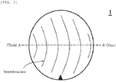
- an SOI wafer 1 having an SOI layer film thickness distribution with a one-way sloping shape having isopachous lines as shown in FIG. 2 can be used.
- FIG. 3 shows diagrams of cross section A-A' after each step when the SOI wafer 1 shown in FIG. 2 is used.
- a method for fabricating an SOI wafer 1 having such an SOI layer 2 with a film thickness distribution with a one-way sloping shape is not particularly limited, but an SOI wafer whose SOI layer came to have a film thickness distribution with a one-way sloping shape as a result of flattening, by a high-temperature long-duration flattening heat treatment, a delaminated surface of the SOI wafer which was delaminated by an ion implantation delamination method, may be used.
- a high-temperature heat treatment furnace for performing such a flattening heat treatment one that is not provided with a wafer rotary mechanism may be used. Since the SOI layer after the flattening heat treatment comes to have a one-way sloping shape depending on conditions such as furnace temperature distribution and heat treatment conditions etc., a heat treatment furnace and heat treatment conditions in which an SOI layer film thickness distribution with a one-way sloping shape is formed are noted experimentally in advance.
- a sacrificial oxidation is often performed as a bonding heat treatment with the object of enhancing a bonding strength while removing the damage on the ion implanted layer.
- the SOI layer immediately after the delamination sometimes comes to have a film thickness distribution with a one-way sloping shape depending on implanting conditions such as an implantation angle (offset angle) at the time of the ion implantation.
- the sacrificial oxidation treatment in the present invention may be applied to the sacrificial oxidation as the bonding heat treatment.
- the SOI layer immediately after polishing sometimes has a film thickness distribution with a one-way sloping shape.
- the SOI wafer after polishing may be used as the SOI wafer 1 whose SOI layer 2 came to have a film thickness distribution with a one-way sloping shape.
- the sacrificial oxidation treatment is performed on the SOI wafer 1 with an SOI layer 2 having a film thickness distribution with a one-way sloping shape, sloping in a particular direction.
- the sacrificial oxidation treatment is performed by a thermal oxidation ( FIG. 1(B) ) and removal of the thermal oxide film ( FIG. 1(C) ).
- the thermal oxidation ( FIG. 1(B) ) in the sacrificial oxidation treatment of the present invention is performed using a vertical heat treatment furnace having a wafer rotary mechanism.
- a non-rotating oxidation is performed using a monitor wafer and the oxide film thickness distribution caused by the non-rotating oxidation is measured beforehand, thereby a thermal oxide film having an oxide film thickness distribution with a one-way sloping shape that corresponds to the one-way sloping shape of the SOI layer can be formed accurately.
- the thermal oxidation in the sacrificial oxidation treatment of the present invention can, by combining a non-rotating oxidation in which a thermal oxidation is performed without rotating the SOI wafer and a rotating oxidation in which a thermal oxidation is performed while rotating the SOI wafer, form a thermal oxide film 3 having an oxide film thickness distribution with a one-way sloping shape on a surface of an SOI layer 2' (( FIG. 1(B) , FIG. 3(B) ).
- the order of the non-rotating oxidation and the rotating oxidation is not particularly limited, but a method of performing the non-rotating oxidation first and then switching to the rotating oxidation is simple and favorable.
- the film thickness distribution of the SOI layer 2 of the SOI wafer (the SOI wafer 1 having a film thickness distribution with a one-way sloping shape) to be subjected to the sacrificial oxidation treatment is measured beforehand, and the introduction direction of the wafer is rotated so that a part where the SOI layer film thickness is greatest (smallest) corresponds to a part where the oxide film thickness distribution of the monitor wafer is greatest(smallest), and then the SOI wafer is set into the wafer boat of the vertical heat treatment furnace.
- the SOI wafer set into the wafer boat is introduced into the vertical heat treatment furnace (oxidation furnace), oxidation is performed for a certain period without rotation, and then, switching to a rotating oxidation, oxidation is performed for a certain period.
- the time when the non-rotating oxidation is switched to the rotating oxidation (that is, the oxidation duration of the non-rotating oxidation) can be experimentally determined taking the SOI layer film thickness distribution before oxidation into consideration so that the film thickness distribution of the SOI layer after the sacrificial oxidation treatment becomes smallest.
- an SOI wafer having an SOI layer whose film thickness distribution with a one-way sloping shape has been resolved is manufactured.
- the method for removing the thermal oxide film is not particularly limited, and a conventional method such as hydrofluoric acid cleaning can be used.
- the present invention is particularly effective when a sacrificial oxidation treatment is performed for canceling the variation of an SOI layer with a radial range of about a few nm at most (typically 1 nm or less) which was formed by an ion implantation delamination method, than when the SOI layer film thickness distribution before oxidation is large to some extent.
- the heat treatment is normally performed at less than 1100°C, mainly at 1050°C or less, and therefore a thermal load is small compared to the flattening heat treatment, and no technical problems arise from the installation of a rotary mechanism.
- an SOI wafer having an SOI layer was fabricated, and by performing a bonding heat treatment and a flattening heat treatment on the SOI wafer under the below-described conditions, an SOI wafer was fabricated.
- Si single crystal wafer diameter: 300 mm, ⁇ 100>,
- the SOI film thickness distribution after the flattening heat treatment was a one-way sloping distribution (a distribution in which the film thickness becomes thinner in a left to right direction with a notch at the bottom) as in FIG. 2 , and a film thickness range (Max-Min) was 0.7 nm.
- a monitor wafer Si single crystal wafer, diameter: 300 mm, ⁇ 100>, p type, 10 ⁇ cm
- the oxide film thickness range was about 5 nm
- the distribution form was, as in FIG. 4 , in a one-way sloping shape, the oxide film thinning from the near side of the furnace towards the far side of the furnace.
- the SOI wafer was set into a wafer boat so that the thickest part of the SOI film thickness was at the near side of the furnace, and in this state, 30 minutes of non-rotating oxidation (1000°C, pyrogenic oxidation) was performed, immediately after which the wafer boat was rotated at a rotational speed of 1 rpm, and then 2 hours of rotating oxidation (1000°C, pyrogenic oxidation) were performed.
- the SOI layer film thickness distribution was measured. As a result, the film thickness distribution with a one-way sloping shape of the SOI layer was resolved, and the film thickness range (Max-Min) was improved to 0.5 nm.
- the sacrificial oxidation treatment was performed under the same conditions as Example 1 except that the sacrificial oxidation was performed with only a rotating oxidation (1 rpm), and the SOI layer film thickness distribution was measured. As a result, the film thickness distribution with a one-way sloping shape of the SOI layer was not resolved, and the film thickness range (Max-Min) had been degraded to 0.9 nm.
- the sacrificial oxidation treatment was performed under the same conditions as Example 1 except that the duration of the non-rotating oxidation and the rotating oxidation (1 rpm) in the sacrificial oxidation was set as shown in Table 1, and the SOI layer film thickness distribution was measured.
- Example 2 resolution of the one-way sloping shape of the SOI layer had progressed compared to before the sacrificial oxidation treatment, the shape was almost uniform, and the film thickness range (Max-Min) had also been improved to 0.6 nm.
Landscapes
- Element Separation (AREA)
- Recrystallisation Techniques (AREA)
- Formation Of Insulating Films (AREA)
Abstract
Description
- The present invention relates to a method for manufacturing an SOI wafer.
- When fabricating an SOI wafer by an ion implantation delamination method, in order to reduce a surface roughness of a delaminated surface while maintaining uniformity of a film thickness of an SOI layer immediately after delamination, a flattening heat treatment which improves surface roughness by performing a high-temperature heat treatment has come to be performed instead of polishing.
- After a flattening heat treatment, normally, a sacrificial oxidation treatment to adjust the SOI layer to a desired film thickness is performed, and in the sacrificial oxidation, as a thermal oxidation furnace that can obtain an oxide film thickness with an excellent radial distribution, a vertical heat treatment furnace capable of performing a thermal oxidation while rotating a wafer is generally used.
- In the flattening heat treatment for improving surface roughness, the greatest advantage is that the uniformity of the film thickness of the SOI layer is not degraded compared to flattening by polishing (touch polishing), but even with the flattening heat treatment, since etching of the SOI layer progresses slightly, compared to the uniformity of the film thickness immediately after delamination, a certain amount of degradation is unavoidable.
- When the film thickness distribution of the SOI layer immediately after the flattening heat treatment is in a concentric circle shape, film thickness distribution of the SOI layer can be improved by the sacrificial oxidation treatment after the flattening heat treatment by adopting a method disclosed in
Patent Document 1. - In
Patent Document 1, it is disclosed that, regarding an SOI film thickness distribution with a concentric circle shape, by performing the thermal oxidation in the sacrificial oxidation treatment during a temperature rise or a temperature fall or both using a batch processing type heat treatment furnace with a wafer rotary mechanism, an oxide film thickness distribution in a concentric circle shape is formed, thereby canceling the SOI film thickness distribution and thereby improving the SOI film thickness distribution. - In addition, in Patent Document 2, it is disclosed that the film thickness distribution of the SOI layer is measured, and based on a predetermined radial stock removal distribution in the thinning step, the thinning is performed in a state in which the wafer is rotated and positioned so that the film thickness distribution of the SOI layer will be improved after the thinning step. However, the thinning step in question is an SC-1 cleaning.
- In addition, in Patent Document 3, it is disclosed that, before performing a thermal oxidation treatment on the SOI layer, a radial film thickness distribution is measured, and based on the measured value, the thermal oxidation treatment is performed with a lamp output adjusted so that a radial temperature of the SOI layer is high in an area where the SOI layer film thickness is thick compared to an area where the SOI layer film thickness is thin.
-
- Patent Document 1: Japanese Unexamined Patent Application Publication No.
2013-125909 - Patent Document 2: Japanese Unexamined Patent Application Publication No.
2016-66692 - Patent Document 3: Japanese Unexamined Patent Application Publication No.
2007-242972 - As stated above, when a film thickness distribution of an SOI layer immediately after performing a flattening heat treatment is in a concentric circle shape, by applying a method disclosed in
Patent Document 1, the film thickness distribution of the SOI layer can be improved with a sacrificial oxidation treatment after the flattening heat treatment. - On the other hand, it has been revealed that, depending on temperature distribution characteristics etc. of a heat treatment furnace in which the flattening heat treatment is performed, the film thickness distribution of the SOI layer after the flattening heat treatment sometimes has a one-way sloping shape (a shape in which an SOI film thickness slopes in a particular direction).
- Even when the SOI layer having a film thickness distribution with such a one-way sloping shape is subjected to a sacrificial oxidation treatment in which a wafer is rotated and an oxide film with a good radial distribution is formed using a vertical heat treatment furnace having a rotary mechanism, the film thickness distribution of the SOI layer cannot be improved by the sacrificial oxidation treatment since the one-way sloping shape of the SOI layer remains.
- The present invention has been accomplished in view of the above-described problems. It is an object of the present invention to provide a method for manufacturing an SOI wafer having an SOI layer whose film thickness distribution with a one-way sloping shape has been resolved by performing a sacrificial oxidation treatment on the SOI wafer having an SOI layer film thickness distribution with the one-way sloping shape.
- To solve the above problems, the present invention provides, a method for manufacturing an SOI wafer by performing a sacrificial oxidation treatment which includes performing a thermal oxidation of an SOI layer surface of an SOI wafer and removing a formed thermal oxide film in order to reduce a thickness of the SOI layer of the SOI wafer, wherein:
- the SOI layer of an SOI wafer on which the sacrificial oxidation treatment is performed has a film thickness distribution with a one-way sloping shape, sloping in a particular direction;
- a thermal oxidation in the sacrificial oxidation treatment is performed by combining a non-rotating oxidation wherein a thermal oxidation is performed without rotating the SOI wafer and a rotating oxidation wherein a thermal oxidation is performed while rotating the SOI wafer, using a vertical heat treatment furnace having a mechanism to rotate a wafer surface in a horizontal direction; whereby a thermal oxide film having an oxide film thickness distribution with a one-way sloping shape canceling the film thickness distribution with a one-way sloping shape of the SOI layer, is formed on a surface of the SOI layer; and
- by removing the formed thermal oxide film, an SOI wafer having an SOI layer whose film thickness distribution with a one-way sloping shape has been resolved is manufactured.
- Such a method for manufacturing an SOI wafer can form an oxide film thickness distribution with a one-way sloping shape that corresponds to the one-way sloping shape of the SOI layer by the thermal oxidation in the sacrificial oxidation treatment, and as a result, the film thickness distribution with the one-way sloping shape of the SOI layer can be canceled, and an SOI wafer having an SOI layer whose film thickness distribution with a one-way sloping shape has been resolved can be manufactured.
- In addition, in this case, as the thermal oxidation in the sacrificial oxidation treatment, it is preferable to perform the rotating oxidation after performing the non-rotating oxidation.
- Thus, by performing the non-rotating oxidation and then switching to the rotating oxidation, an oxide film thickness distribution with a one-way sloping shape that corresponds to the one-way sloping shape of the SOI layer can be formed easily, and therefore, it is preferable.
- In addition, in this case, the SOI wafer with the SOI layer having a film thickness distribution with the one-way sloping shape can be fabricated by adding a flattening heat treatment for flattening the SOI layer surface which was delaminated at the ion implanted layer by an ion implantation delamination method.
- Thus, as the SOI wafer to be subjected to the sacrificial oxidation treatment, an SOI wafer whose SOI layer came to have a film thickness distribution with a one-way sloping shape as a result of adding the flattening heat treatment after the delamination by the ion implantation delamination method can be used.
- The inventive method for manufacturing an SOI wafer can, by performing a thermal oxidation in the sacrificial oxidation treatment, combining a non-rotating oxidation and a rotating oxidation, form an oxide film thickness distribution with a one-way sloping shape that corresponds to the one-way sloping shape of the SOI layer, and as a result, the SOI layer film thickness distribution can be canceled, and an SOI wafer having an SOI layer whose film thickness distribution with a one-way sloping shape has been resolved can be manufactured.
-
-
FIG. 1 is a flow diagram showing an example of the inventive method for manufacturing an SOI wafer. -
FIG. 2 is a diagram showing an example of an SOI wafer whose SOI layer has a film thickness distribution with a one-way sloping shape, sloping in a particular direction which is subjected to a sacrificial oxidation treatment in the present invention. -
FIG. 3 shows cross section A-A' after each step in the inventive method for manufacturing an SOI wafer when the SOI wafer shown inFIG. 2 is used as the SOI wafer to be subjected to the sacrificial oxidation treatment. -
FIG. 4 is a diagram showing an oxide film thickness distribution formed on the monitor wafer by only a non-rotating oxidation in the vertical heat treatment furnace used in Examples and Comparative Examples. - As stated above, even when the SOI layer having a film thickness distribution with such a one-way sloping shape is subjected to a sacrificial oxidation treatment in which a wafer is rotated and an oxide film with a good radial distribution is formed using a vertical heat treatment furnace having a rotary mechanism, the film thickness distribution of the SOI layer cannot be improved by the sacrificial oxidation treatment since the one-way sloping shape of the SOI layer remains.
- The present inventor has studied diligently to solve the above problem and consequently found that, when an SOI wafer having an SOI layer film thickness distribution with a one-way sloping shape is subjected to a sacrificial oxidation using a vertical heat treatment furnace having a wafer rotary mechanism, by combining a non-rotating oxidation in which a thermal oxidation is performed without rotating the wafer and a rotating oxidation in which a thermal oxidation is performed while rotating the wafer, a thermal oxide film having an oxide film thickness distribution with a one-way sloping shape that cancels the SOI layer film thickness distribution is formed on the surface of the SOI layer, thereby, after the sacrificial oxidation treatment, an SOI wafer having an SOI layer whose film thickness distribution with a one-way sloping shape has been resolved can be manufactured, and arrived at the present invention.
- That is, the present invention provides a method for manufacturing an SOI wafer by performing a sacrificial oxidation treatment which includes performing a thermal oxidation of an SOI layer surface of an SOI wafer and removing a formed thermal oxide film in order to reduce a thickness of the SOI layer of the SOI wafer, wherein:
- the SOI layer of an SOI wafer on which the sacrificial oxidation treatment is performed has a film thickness distribution with a one-way sloping shape, sloping in a particular direction;
- a thermal oxidation in the sacrificial oxidation treatment is performed by combining a non-rotating oxidation wherein a thermal oxidation is performed without rotating the SOI wafer and a rotating oxidation wherein a thermal oxidation is performed while rotating the SOI wafer, using a vertical heat treatment furnace having a mechanism to rotate a wafer surface in a horizontal direction;
- whereby a thermal oxide film having an oxide film thickness distribution with a one-way sloping shape canceling the film thickness distribution with a one-way sloping shape of the SOI layer, is formed on a surface of the SOI layer; and
- by removing the formed thermal oxide film, an SOI wafer having an SOI layer whose film thickness distribution with a one-way sloping shape has been resolved is manufactured.
- Hereinafter, the inventive method for manufacturing an SOI wafer will be described. A flow diagram showing an example of the inventive method for manufacturing an SOI wafer is shown in
FIG. 1 . - In the present invention, first, as the SOI wafer on which the sacrificial oxidation treatment is to be performed, an SOI wafer 1 with an SOI layer 2 having a film thickness distribution with a one-way sloping shape, sloping in a particular direction is prepared (
FIG. 1(A) ,FIG. 3(A) ). For example, anSOI wafer 1 having an SOI layer film thickness distribution with a one-way sloping shape having isopachous lines as shown inFIG. 2 can be used. It is to be noted thatFIG. 3 shows diagrams of cross section A-A' after each step when theSOI wafer 1 shown inFIG. 2 is used. - A method for fabricating an
SOI wafer 1 having such an SOI layer 2 with a film thickness distribution with a one-way sloping shape is not particularly limited, but an SOI wafer whose SOI layer came to have a film thickness distribution with a one-way sloping shape as a result of flattening, by a high-temperature long-duration flattening heat treatment, a delaminated surface of the SOI wafer which was delaminated by an ion implantation delamination method, may be used. - As a high-temperature heat treatment furnace for performing such a flattening heat treatment, one that is not provided with a wafer rotary mechanism may be used. Since the SOI layer after the flattening heat treatment comes to have a one-way sloping shape depending on conditions such as furnace temperature distribution and heat treatment conditions etc., a heat treatment furnace and heat treatment conditions in which an SOI layer film thickness distribution with a one-way sloping shape is formed are noted experimentally in advance.
- In addition, after the delamination at the ion implanted layer and before the flattening heat treatment, a sacrificial oxidation is often performed as a bonding heat treatment with the object of enhancing a bonding strength while removing the damage on the ion implanted layer. In such a case, the SOI layer immediately after the delamination sometimes comes to have a film thickness distribution with a one-way sloping shape depending on implanting conditions such as an implantation angle (offset angle) at the time of the ion implantation. In such a case, the sacrificial oxidation treatment in the present invention may be applied to the sacrificial oxidation as the bonding heat treatment.
- In addition, when the flatting is performed by polishing (touch polishing), depending on polishing conditions, the SOI layer immediately after polishing sometimes has a film thickness distribution with a one-way sloping shape. In such a case, the SOI wafer after polishing may be used as the
SOI wafer 1 whose SOI layer 2 came to have a film thickness distribution with a one-way sloping shape. - Subsequently, the sacrificial oxidation treatment is performed on the
SOI wafer 1 with an SOI layer 2 having a film thickness distribution with a one-way sloping shape, sloping in a particular direction. The sacrificial oxidation treatment is performed by a thermal oxidation (FIG. 1(B) ) and removal of the thermal oxide film (FIG. 1(C) ). - The thermal oxidation (
FIG. 1(B) ) in the sacrificial oxidation treatment of the present invention is performed using a vertical heat treatment furnace having a wafer rotary mechanism. - In the present invention, using an oxidation furnace having a rotary mechanism to be used, a non-rotating oxidation is performed using a monitor wafer and the oxide film thickness distribution caused by the non-rotating oxidation is measured beforehand, thereby a thermal oxide film having an oxide film thickness distribution with a one-way sloping shape that corresponds to the one-way sloping shape of the SOI layer can be formed accurately.
- The thermal oxidation in the sacrificial oxidation treatment of the present invention can, by combining a non-rotating oxidation in which a thermal oxidation is performed without rotating the SOI wafer and a rotating oxidation in which a thermal oxidation is performed while rotating the SOI wafer, form a thermal oxide film 3 having an oxide film thickness distribution with a one-way sloping shape on a surface of an SOI layer 2' ((
FIG. 1(B) ,FIG. 3(B) ). It is to be noted that the order of the non-rotating oxidation and the rotating oxidation is not particularly limited, but a method of performing the non-rotating oxidation first and then switching to the rotating oxidation is simple and favorable. - When the non-rotating oxidation is performed first, the film thickness distribution of the SOI layer 2 of the SOI wafer (the
SOI wafer 1 having a film thickness distribution with a one-way sloping shape) to be subjected to the sacrificial oxidation treatment is measured beforehand, and the introduction direction of the wafer is rotated so that a part where the SOI layer film thickness is greatest (smallest) corresponds to a part where the oxide film thickness distribution of the monitor wafer is greatest(smallest), and then the SOI wafer is set into the wafer boat of the vertical heat treatment furnace. - The SOI wafer set into the wafer boat is introduced into the vertical heat treatment furnace (oxidation furnace), oxidation is performed for a certain period without rotation, and then, switching to a rotating oxidation, oxidation is performed for a certain period. The time when the non-rotating oxidation is switched to the rotating oxidation (that is, the oxidation duration of the non-rotating oxidation) can be experimentally determined taking the SOI layer film thickness distribution before oxidation into consideration so that the film thickness distribution of the SOI layer after the sacrificial oxidation treatment becomes smallest.
- In addition, the order of the non-rotating oxidation and the rotating oxidation is not particularly limited in the present invention, and if the position in which to stop the wafer when beginning the non-rotating oxidation can be perceived, it is also possible to perform the non-rotating oxidation after the rotating oxidation, and they can also be repeated one after the other several times.
- Next, by removing the formed thermal oxide film 3 (
FIG. 1(C) ,FIG. 3(C) ), an SOI wafer having an SOI layer whose film thickness distribution with a one-way sloping shape has been resolved is manufactured. The method for removing the thermal oxide film is not particularly limited, and a conventional method such as hydrofluoric acid cleaning can be used. - The present invention is particularly effective when a sacrificial oxidation treatment is performed for canceling the variation of an SOI layer with a radial range of about a few nm at most (typically 1 nm or less) which was formed by an ion implantation delamination method, than when the SOI layer film thickness distribution before oxidation is large to some extent.
- It is to be noted that if a rotary mechanism is installed in a heat treatment furnace for performing the flattening heat treatment at a high temperature for a long duration, an SOI layer after the flattening heat treatment can be obtained in a near concentric circle shape, but with a heat treatment furnace for performing a heat treatment at a high temperature for a long duration that is not provided with a rotary mechanism, there is no danger of the cost of the device itself rising in connection to the installation of the rotary mechanism, and in addition, there is no danger of becoming liable to malfunctions etc. due to effects from deformation of a heat treatment tube etc. and therefore, it is favorable.
- In contrast, with a vertical heat treatment furnace (oxidation furnace) used for the thermal oxidation in the sacrificial oxidation treatment, often, the heat treatment is normally performed at less than 1100°C, mainly at 1050°C or less, and therefore a thermal load is small compared to the flattening heat treatment, and no technical problems arise from the installation of a rotary mechanism.
- In addition, even when a heat treatment furnace with a rotary mechanism installed is used as the heat treatment furnace for performing the flattening heat treatment at a high temperature for a long duration, there is a possibility that a film thickness distribution with a one-way sloping shape is slightly formed depending on conditions such as furnace temperature distribution, deviation in the center of rotation, or heat treatment conditions etc. Even in such a case, it is possible to apply the present invention, and by applying the non-rotating oxidation for a relatively short time, obtain an adjusting effect of the SOI layer film thickness distribution.
- Hereinafter, the present invention will be more specifically described with reference to Examples and Comparative Examples. However, the present invention is not limited to these Examples.
- By forming an ion implanted layer on the surface of a below-described bond wafer (with a thermal oxide film) under the below-described ion implanting conditions, bonding to the surface of a below-described base wafer with the thermal oxide film interposed therebetween, and then performing a delaminating heat treatment under the below-described conditions and delaminating the bond wafer at the ion implanted layer, an SOI wafer having an SOI layer was fabricated, and by performing a bonding heat treatment and a flattening heat treatment on the SOI wafer under the below-described conditions, an SOI wafer was fabricated.
-
- Si single crystal wafer, diameter: 300 mm, <100>, p type, 10 Ω cm
- With thermal oxide film of 25 nm
- Si single crystal wafer, diameter: 300 mm, <100>,
- H+ ion, 50 keV, 6×10¹⁶/cm2
- (Delaminating heat treatment) 500°C, 30 minutes, nitrogen atmosphere
- (Bonding heat treatment) 1050°C, 1 hour, oxidizing atmosphere
- (Flattening treatment) 1200°C, 3 hours, H2 gas 100%
- The SOI film thickness distribution after the flattening heat treatment was a one-way sloping distribution (a distribution in which the film thickness becomes thinner in a left to right direction with a notch at the bottom) as in
FIG. 2 , and a film thickness range (Max-Min) was 0.7 nm. - In the sacrificial oxidation conditions (1000°C, pyrogenic oxidation, forming oxide film of about 410 nm) to perform on the above-described SOI wafer, a monitor wafer (Si single crystal wafer, diameter: 300 mm, <100>, p type, 10 Ω cm) was used to measure the oxide film thickness distribution formed only with the non-rotating oxidation. As a result, it was observed that the oxide film thickness range was about 5 nm, and the distribution form was, as in
FIG. 4 , in a one-way sloping shape, the oxide film thinning from the near side of the furnace towards the far side of the furnace. - The SOI wafer was set into a wafer boat so that the thickest part of the SOI film thickness was at the near side of the furnace, and in this state, 30 minutes of non-rotating oxidation (1000°C, pyrogenic oxidation) was performed, immediately after which the wafer boat was rotated at a rotational speed of 1 rpm, and then 2 hours of rotating oxidation (1000°C, pyrogenic oxidation) were performed. After removing the oxide film on the surface of the SOI layer by immersing the SOI wafer after finishing the sacrificial oxidation in dilute hydrofluoric acid, the SOI layer film thickness distribution was measured. As a result, the film thickness distribution with a one-way sloping shape of the SOI layer was resolved, and the film thickness range (Max-Min) was improved to 0.5 nm.
- The sacrificial oxidation treatment was performed under the same conditions as Example 1 except that the sacrificial oxidation was performed with only a rotating oxidation (1 rpm), and the SOI layer film thickness distribution was measured. As a result, the film thickness distribution with a one-way sloping shape of the SOI layer was not resolved, and the film thickness range (Max-Min) had been degraded to 0.9 nm.
- The sacrificial oxidation treatment was performed under the same conditions as Example 1 except that the duration of the non-rotating oxidation and the rotating oxidation (1 rpm) in the sacrificial oxidation was set as shown in Table 1, and the SOI layer film thickness distribution was measured. In Example 2, resolution of the one-way sloping shape of the SOI layer had progressed compared to before the sacrificial oxidation treatment, the shape was almost uniform, and the film thickness range (Max-Min) had also been improved to 0.6 nm. In addition, in Comparative Examples 2 to 4, the one-way sloping shape had sloped in the opposite direction, having gone beyond canceling the film thickness distribution with the one-way sloping shape of the SOI layer, and the film thickness range (Max-Min) had also been degraded.
- The film thickness range of the SOI wafer manufactured in Examples 1, 2, and Comparative Examples 1 to 4 and the SOI layer film thickness distribution shape are shown in Table 1.
[Table 1] Comparative Example 1 Example 2 Example 1 Comparative Example 2 Comparative Example 3 Comparative Example 4 Duration of non-rotating oxidation (minutes) 0 15 30 45 60 150 Duration of rotating oxidation (minutes) 150 135 120 105 90 0 SOI film thickness range 0.9 nm 0.6 nm 0.5 nm 0.7 nm 1.2 nm 2.5 nm SOI film thickness distribution shape One-way sloping Uniform Uniform One-way sloping One-way sloping One-way sloping - It should be noted that the present invention is not limited to the above-described embodiments. The embodiments are just examples, and any examples that have substantially the same feature and demonstrate the same functions and effects as those in the technical concept disclosed in claims of the present invention are included in the technical scope of the present invention.
Claims (3)
- A method for manufacturing an SOI wafer by performing a sacrificial oxidation treatment which includes performing a thermal oxidation of an SOI layer surface of an SOI wafer and removing a formed thermal oxide film in order to reduce a thickness of the SOI layer of the SOI wafer, wherein:the SOI layer of an SOI wafer on which the sacrificial oxidation treatment is performed has a film thickness distribution with a one-way sloping shape, sloping in a particular direction;a thermal oxidation in the sacrificial oxidation treatment is performed by combining a non-rotating oxidation wherein a thermal oxidation is performed without rotating the SOI wafer and a rotating oxidation wherein a thermal oxidation is performed while rotating the SOI wafer, using a vertical heat treatment furnace having a mechanism to rotate a wafer surface in a horizontal direction;whereby a thermal oxide film having an oxide film thickness distribution with a one-way sloping shape canceling the film thickness distribution with a one-way sloping shape of the SOI layer, is formed on a surface of the SOI layer; andby removing the formed thermal oxide film, an SOI wafer having an SOI layer whose film thickness distribution with a one-way sloping shape has been resolved is manufactured.
- The method for manufacturing an SOI wafer according to claim 1, wherein, as a thermal oxidation in the sacrificial oxidation treatment, the rotating oxidation is performed after the non-rotating oxidation is performed.
- The method for manufacturing an SOI wafer according to claim 1 or 2, wherein the SOI wafer with the SOI layer having a film thickness distribution with the one-way sloping shape is fabricated by adding a flattening heat treatment for flattening an SOI layer surface which was delaminated at the ion implanted layer by an ion implantation delamination method.
Applications Claiming Priority (2)
| Application Number | Priority Date | Filing Date | Title |
|---|---|---|---|
| JP2017123117A JP6747386B2 (en) | 2017-06-23 | 2017-06-23 | Method for manufacturing SOI wafer |
| PCT/JP2018/020640 WO2018235548A1 (en) | 2017-06-23 | 2018-05-30 | Soi wafer manufacturing method |
Publications (2)
| Publication Number | Publication Date |
|---|---|
| EP3644346A1 true EP3644346A1 (en) | 2020-04-29 |
| EP3644346A4 EP3644346A4 (en) | 2021-03-17 |
Family
ID=64737470
Family Applications (1)
| Application Number | Title | Priority Date | Filing Date |
|---|---|---|---|
| EP18820765.8A Pending EP3644346A4 (en) | 2017-06-23 | 2018-05-30 | SELF-SLICE MANUFACTURING PROCESS |
Country Status (8)
| Country | Link |
|---|---|
| US (1) | US11244851B2 (en) |
| EP (1) | EP3644346A4 (en) |
| JP (1) | JP6747386B2 (en) |
| KR (1) | KR102554190B1 (en) |
| CN (1) | CN110785830B (en) |
| SG (1) | SG11201911688XA (en) |
| TW (1) | TWI774781B (en) |
| WO (1) | WO2018235548A1 (en) |
Family Cites Families (10)
| Publication number | Priority date | Publication date | Assignee | Title |
|---|---|---|---|---|
| JPH0750234A (en) * | 1993-08-04 | 1995-02-21 | Komatsu Electron Metals Co Ltd | Semiconductor wafer manufacturing device and method |
| EP2190010A2 (en) * | 2002-08-12 | 2010-05-26 | S.O.I. Tec Silicon on Insulator Technologies | A method of preparing a thin layer of semiconductor material |
| US20040087042A1 (en) * | 2002-08-12 | 2004-05-06 | Bruno Ghyselen | Method and apparatus for adjusting the thickness of a layer of semiconductor material |
| JP2007123643A (en) | 2005-10-31 | 2007-05-17 | Matsushita Electric Ind Co Ltd | Film forming apparatus, film forming method, film forming apparatus monitoring program, and recording medium therefor |
| JP2007242972A (en) * | 2006-03-09 | 2007-09-20 | Shin Etsu Handotai Co Ltd | Manufacturing method for soi wafer |
| JP2010153809A (en) | 2008-11-26 | 2010-07-08 | Sumco Corp | Method of making uniform distribution of layer of predetermined thickness formed on silicon wafer and, and method of making uniform distribution of thickness of the silicon wafer |
| JP5927894B2 (en) * | 2011-12-15 | 2016-06-01 | 信越半導体株式会社 | Manufacturing method of SOI wafer |
| FR3007891B1 (en) | 2013-06-28 | 2016-11-25 | Soitec Silicon On Insulator | METHOD FOR MANUFACTURING A COMPOSITE STRUCTURE |
| JP6107709B2 (en) * | 2014-03-10 | 2017-04-05 | 信越半導体株式会社 | Manufacturing method of bonded SOI wafer |
| JP6086105B2 (en) * | 2014-09-24 | 2017-03-01 | 信越半導体株式会社 | Manufacturing method of SOI wafer |
-
2017
- 2017-06-23 JP JP2017123117A patent/JP6747386B2/en active Active
-
2018
- 2018-05-30 KR KR1020197037214A patent/KR102554190B1/en active Active
- 2018-05-30 CN CN201880038871.9A patent/CN110785830B/en active Active
- 2018-05-30 SG SG11201911688XA patent/SG11201911688XA/en unknown
- 2018-05-30 EP EP18820765.8A patent/EP3644346A4/en active Pending
- 2018-05-30 US US16/621,001 patent/US11244851B2/en active Active
- 2018-05-30 WO PCT/JP2018/020640 patent/WO2018235548A1/en not_active Ceased
- 2018-06-05 TW TW107119237A patent/TWI774781B/en active
Also Published As
| Publication number | Publication date |
|---|---|
| CN110785830A (en) | 2020-02-11 |
| TW201905962A (en) | 2019-02-01 |
| JP6747386B2 (en) | 2020-08-26 |
| EP3644346A4 (en) | 2021-03-17 |
| SG11201911688XA (en) | 2020-01-30 |
| US20200111701A1 (en) | 2020-04-09 |
| US11244851B2 (en) | 2022-02-08 |
| JP2019009257A (en) | 2019-01-17 |
| CN110785830B (en) | 2023-09-22 |
| KR20200019142A (en) | 2020-02-21 |
| WO2018235548A1 (en) | 2018-12-27 |
| TWI774781B (en) | 2022-08-21 |
| KR102554190B1 (en) | 2023-07-12 |
Similar Documents
| Publication | Publication Date | Title |
|---|---|---|
| JP4830290B2 (en) | Manufacturing method of directly bonded wafer | |
| EP2793250B1 (en) | Soi wafer fabrication method | |
| EP3104395B1 (en) | Method for manufacturing laminated wafer | |
| EP3309819B1 (en) | Bonded soi wafer manufacturing method | |
| EP2151851B1 (en) | Method for forming silicon oxide film of soi wafer | |
| JP4442560B2 (en) | Manufacturing method of SOI wafer | |
| EP2887383B1 (en) | Soi wafer manufacturing method | |
| EP2717294B1 (en) | Method for manufacturing bonded wafer | |
| EP3522202B1 (en) | Bonded soi wafer manufacturing method | |
| US11244851B2 (en) | Method for manufacturing SOI wafer | |
| KR101543748B1 (en) | Soi wafer manufacturing method | |
| JP2016201454A (en) | Manufacturing method of SOI wafer | |
| JP5531642B2 (en) | Manufacturing method of bonded wafer | |
| EP3159911B1 (en) | Method for manufacturing soi wafer | |
| JP2001093789A (en) | Method for manufacturing bonded soi wafer | |
| JP5555995B2 (en) | Method for manufacturing bonded silicon wafer | |
| JP2006013179A (en) | Method for manufacturing soi wafer |
Legal Events
| Date | Code | Title | Description |
|---|---|---|---|
| STAA | Information on the status of an ep patent application or granted ep patent |
Free format text: STATUS: THE INTERNATIONAL PUBLICATION HAS BEEN MADE |
|
| PUAI | Public reference made under article 153(3) epc to a published international application that has entered the european phase |
Free format text: ORIGINAL CODE: 0009012 |
|
| STAA | Information on the status of an ep patent application or granted ep patent |
Free format text: STATUS: REQUEST FOR EXAMINATION WAS MADE |
|
| 17P | Request for examination filed |
Effective date: 20191218 |
|
| AK | Designated contracting states |
Kind code of ref document: A1 Designated state(s): AL AT BE BG CH CY CZ DE DK EE ES FI FR GB GR HR HU IE IS IT LI LT LU LV MC MK MT NL NO PL PT RO RS SE SI SK SM TR |
|
| AX | Request for extension of the european patent |
Extension state: BA ME |
|
| DAV | Request for validation of the european patent (deleted) | ||
| DAX | Request for extension of the european patent (deleted) | ||
| A4 | Supplementary search report drawn up and despatched |
Effective date: 20210217 |
|
| RIC1 | Information provided on ipc code assigned before grant |
Ipc: H01L 21/265 20060101ALI20210211BHEP Ipc: H01L 27/12 20060101ALI20210211BHEP Ipc: H01L 21/306 20060101ALI20210211BHEP Ipc: H01L 21/324 20060101ALI20210211BHEP Ipc: H01L 21/02 20060101AFI20210211BHEP |
|
| STAA | Information on the status of an ep patent application or granted ep patent |
Free format text: STATUS: EXAMINATION IS IN PROGRESS |
|
| 17Q | First examination report despatched |
Effective date: 20240506 |