EP3644049A1 - Topographically structured support for electron crystallography - Google Patents
Topographically structured support for electron crystallography Download PDFInfo
- Publication number
- EP3644049A1 EP3644049A1 EP18202868.8A EP18202868A EP3644049A1 EP 3644049 A1 EP3644049 A1 EP 3644049A1 EP 18202868 A EP18202868 A EP 18202868A EP 3644049 A1 EP3644049 A1 EP 3644049A1
- Authority
- EP
- European Patent Office
- Prior art keywords
- data
- sample
- crystals
- sample support
- carbon
- Prior art date
- Legal status (The legal status is an assumption and is not a legal conclusion. Google has not performed a legal analysis and makes no representation as to the accuracy of the status listed.)
- Withdrawn
Links
- 238000002003 electron diffraction Methods 0.000 title claims description 11
- 239000000523 sample Substances 0.000 claims abstract description 64
- 238000000034 method Methods 0.000 claims abstract description 16
- 238000003384 imaging method Methods 0.000 claims abstract description 4
- OKTJSMMVPCPJKN-UHFFFAOYSA-N Carbon Chemical compound [C] OKTJSMMVPCPJKN-UHFFFAOYSA-N 0.000 claims description 29
- 229910052799 carbon Inorganic materials 0.000 claims description 27
- 239000004677 Nylon Substances 0.000 claims description 20
- 229920001778 nylon Polymers 0.000 claims description 20
- 230000001680 brushing effect Effects 0.000 claims description 8
- 239000002071 nanotube Substances 0.000 claims description 5
- 239000004033 plastic Substances 0.000 claims description 5
- -1 nylon Chemical compound 0.000 claims description 2
- 239000013078 crystal Substances 0.000 abstract description 51
- 230000008021 deposition Effects 0.000 abstract description 5
- 239000000835 fiber Substances 0.000 description 8
- HEMHJVSKTPXQMS-UHFFFAOYSA-M Sodium hydroxide Chemical compound [OH-].[Na+] HEMHJVSKTPXQMS-UHFFFAOYSA-M 0.000 description 6
- 229910021536 Zeolite Inorganic materials 0.000 description 6
- 230000005540 biological transmission Effects 0.000 description 6
- HNPSIPDUKPIQMN-UHFFFAOYSA-N dioxosilane;oxo(oxoalumanyloxy)alumane Chemical compound O=[Si]=O.O=[Al]O[Al]=O HNPSIPDUKPIQMN-UHFFFAOYSA-N 0.000 description 6
- 239000010457 zeolite Substances 0.000 description 6
- 238000003917 TEM image Methods 0.000 description 5
- 238000013459 approach Methods 0.000 description 4
- 238000002447 crystallographic data Methods 0.000 description 4
- 239000002121 nanofiber Substances 0.000 description 4
- 239000002245 particle Substances 0.000 description 4
- 238000002360 preparation method Methods 0.000 description 4
- XLYOFNOQVPJJNP-UHFFFAOYSA-N water Substances O XLYOFNOQVPJJNP-UHFFFAOYSA-N 0.000 description 4
- 239000010949 copper Substances 0.000 description 3
- 238000002050 diffraction method Methods 0.000 description 3
- 239000000463 material Substances 0.000 description 3
- 229910001220 stainless steel Inorganic materials 0.000 description 3
- 239000010935 stainless steel Substances 0.000 description 3
- 238000002424 x-ray crystallography Methods 0.000 description 3
- RYGMFSIKBFXOCR-UHFFFAOYSA-N Copper Chemical compound [Cu] RYGMFSIKBFXOCR-UHFFFAOYSA-N 0.000 description 2
- VYPSYNLAJGMNEJ-UHFFFAOYSA-N Silicium dioxide Chemical compound O=[Si]=O VYPSYNLAJGMNEJ-UHFFFAOYSA-N 0.000 description 2
- 238000005162 X-ray Laue diffraction Methods 0.000 description 2
- 238000005119 centrifugation Methods 0.000 description 2
- 230000000739 chaotic effect Effects 0.000 description 2
- 229910052802 copper Inorganic materials 0.000 description 2
- 239000008367 deionised water Substances 0.000 description 2
- 229910021641 deionized water Inorganic materials 0.000 description 2
- 238000010894 electron beam technology Methods 0.000 description 2
- 238000001493 electron microscopy Methods 0.000 description 2
- 238000001523 electrospinning Methods 0.000 description 2
- 238000005421 electrostatic potential Methods 0.000 description 2
- BDAGIHXWWSANSR-UHFFFAOYSA-N methanoic acid Natural products OC=O BDAGIHXWWSANSR-UHFFFAOYSA-N 0.000 description 2
- 239000000203 mixture Substances 0.000 description 2
- 239000002159 nanocrystal Substances 0.000 description 2
- 102000004169 proteins and genes Human genes 0.000 description 2
- 108090000623 proteins and genes Proteins 0.000 description 2
- 230000005855 radiation Effects 0.000 description 2
- 238000005070 sampling Methods 0.000 description 2
- LPSKDVINWQNWFE-UHFFFAOYSA-M tetrapropylazanium;hydroxide Chemical compound [OH-].CCC[N+](CCC)(CCC)CCC LPSKDVINWQNWFE-UHFFFAOYSA-M 0.000 description 2
- 238000003325 tomography Methods 0.000 description 2
- 229910001868 water Inorganic materials 0.000 description 2
- XNDZQQSKSQTQQD-UHFFFAOYSA-N 3-methylcyclohex-2-en-1-ol Chemical compound CC1=CC(O)CCC1 XNDZQQSKSQTQQD-UHFFFAOYSA-N 0.000 description 1
- OSWFIVFLDKOXQC-UHFFFAOYSA-N 4-(3-methoxyphenyl)aniline Chemical compound COC1=CC=CC(C=2C=CC(N)=CC=2)=C1 OSWFIVFLDKOXQC-UHFFFAOYSA-N 0.000 description 1
- 238000012935 Averaging Methods 0.000 description 1
- 229920000049 Carbon (fiber) Polymers 0.000 description 1
- 229920002292 Nylon 6 Polymers 0.000 description 1
- 239000004809 Teflon Substances 0.000 description 1
- 229920006362 Teflon® Polymers 0.000 description 1
- BOTDANWDWHJENH-UHFFFAOYSA-N Tetraethyl orthosilicate Chemical compound CCO[Si](OCC)(OCC)OCC BOTDANWDWHJENH-UHFFFAOYSA-N 0.000 description 1
- PNEYBMLMFCGWSK-UHFFFAOYSA-N aluminium oxide Inorganic materials [O-2].[O-2].[O-2].[Al+3].[Al+3] PNEYBMLMFCGWSK-UHFFFAOYSA-N 0.000 description 1
- 238000004458 analytical method Methods 0.000 description 1
- 230000003466 anti-cipated effect Effects 0.000 description 1
- 239000004917 carbon fiber Substances 0.000 description 1
- 239000002041 carbon nanotube Substances 0.000 description 1
- 229910021393 carbon nanotube Inorganic materials 0.000 description 1
- 229910052681 coesite Inorganic materials 0.000 description 1
- 150000001875 compounds Chemical class 0.000 description 1
- 238000001816 cooling Methods 0.000 description 1
- 229910052593 corundum Inorganic materials 0.000 description 1
- 229910052906 cristobalite Inorganic materials 0.000 description 1
- 238000002425 crystallisation Methods 0.000 description 1
- 230000008025 crystallization Effects 0.000 description 1
- 238000007405 data analysis Methods 0.000 description 1
- 238000013461 design Methods 0.000 description 1
- 230000006866 deterioration Effects 0.000 description 1
- 239000006185 dispersion Substances 0.000 description 1
- 238000006073 displacement reaction Methods 0.000 description 1
- 239000000428 dust Substances 0.000 description 1
- 230000000694 effects Effects 0.000 description 1
- 230000005670 electromagnetic radiation Effects 0.000 description 1
- JROGBPMEKVAPEH-GXGBFOEMSA-N emetine dihydrochloride Chemical compound Cl.Cl.N1CCC2=CC(OC)=C(OC)C=C2[C@H]1C[C@H]1C[C@H]2C3=CC(OC)=C(OC)C=C3CCN2C[C@@H]1CC JROGBPMEKVAPEH-GXGBFOEMSA-N 0.000 description 1
- 238000013213 extrapolation Methods 0.000 description 1
- 235000019253 formic acid Nutrition 0.000 description 1
- PCHJSUWPFVWCPO-UHFFFAOYSA-N gold Chemical compound [Au] PCHJSUWPFVWCPO-UHFFFAOYSA-N 0.000 description 1
- 229910052737 gold Inorganic materials 0.000 description 1
- 239000010931 gold Substances 0.000 description 1
- 229910021389 graphene Inorganic materials 0.000 description 1
- 230000010354 integration Effects 0.000 description 1
- 230000003993 interaction Effects 0.000 description 1
- 238000011835 investigation Methods 0.000 description 1
- 238000010884 ion-beam technique Methods 0.000 description 1
- 238000002386 leaching Methods 0.000 description 1
- 239000007788 liquid Substances 0.000 description 1
- 239000008204 material by function Substances 0.000 description 1
- 238000005259 measurement Methods 0.000 description 1
- 238000001000 micrograph Methods 0.000 description 1
- 238000003801 milling Methods 0.000 description 1
- 238000012986 modification Methods 0.000 description 1
- 230000004048 modification Effects 0.000 description 1
- 230000003287 optical effect Effects 0.000 description 1
- 230000010355 oscillation Effects 0.000 description 1
- 239000008188 pellet Substances 0.000 description 1
- 230000000149 penetrating effect Effects 0.000 description 1
- 238000000634 powder X-ray diffraction Methods 0.000 description 1
- 238000012545 processing Methods 0.000 description 1
- 239000011347 resin Substances 0.000 description 1
- 229920005989 resin Polymers 0.000 description 1
- 239000000377 silicon dioxide Substances 0.000 description 1
- 238000003756 stirring Methods 0.000 description 1
- 229910052682 stishovite Inorganic materials 0.000 description 1
- 230000009897 systematic effect Effects 0.000 description 1
- 229910052905 tridymite Inorganic materials 0.000 description 1
- 238000004017 vitrification Methods 0.000 description 1
- 229910001845 yogo sapphire Inorganic materials 0.000 description 1
Images


Classifications
-
- G—PHYSICS
- G01—MEASURING; TESTING
- G01N—INVESTIGATING OR ANALYSING MATERIALS BY DETERMINING THEIR CHEMICAL OR PHYSICAL PROPERTIES
- G01N23/00—Investigating or analysing materials by the use of wave or particle radiation, e.g. X-rays or neutrons, not covered by groups G01N3/00 – G01N17/00, G01N21/00 or G01N22/00
- G01N23/20—Investigating or analysing materials by the use of wave or particle radiation, e.g. X-rays or neutrons, not covered by groups G01N3/00 – G01N17/00, G01N21/00 or G01N22/00 by using diffraction of the radiation by the materials, e.g. for investigating crystal structure; by using scattering of the radiation by the materials, e.g. for investigating non-crystalline materials; by using reflection of the radiation by the materials
- G01N23/20008—Constructional details of analysers, e.g. characterised by X-ray source, detector or optical system; Accessories therefor; Preparing specimens therefor
- G01N23/20025—Sample holders or supports therefor
-
- H—ELECTRICITY
- H01—ELECTRIC ELEMENTS
- H01J—ELECTRIC DISCHARGE TUBES OR DISCHARGE LAMPS
- H01J37/00—Discharge tubes with provision for introducing objects or material to be exposed to the discharge, e.g. for the purpose of examination or processing thereof
- H01J37/02—Details
- H01J37/20—Means for supporting or positioning the object or the material; Means for adjusting diaphragms or lenses associated with the support
-
- H—ELECTRICITY
- H01—ELECTRIC ELEMENTS
- H01J—ELECTRIC DISCHARGE TUBES OR DISCHARGE LAMPS
- H01J37/00—Discharge tubes with provision for introducing objects or material to be exposed to the discharge, e.g. for the purpose of examination or processing thereof
- H01J37/26—Electron or ion microscopes; Electron or ion diffraction tubes
- H01J37/295—Electron or ion diffraction tubes
-
- G—PHYSICS
- G01—MEASURING; TESTING
- G01N—INVESTIGATING OR ANALYSING MATERIALS BY DETERMINING THEIR CHEMICAL OR PHYSICAL PROPERTIES
- G01N23/00—Investigating or analysing materials by the use of wave or particle radiation, e.g. X-rays or neutrons, not covered by groups G01N3/00 – G01N17/00, G01N21/00 or G01N22/00
- G01N23/20—Investigating or analysing materials by the use of wave or particle radiation, e.g. X-rays or neutrons, not covered by groups G01N3/00 – G01N17/00, G01N21/00 or G01N22/00 by using diffraction of the radiation by the materials, e.g. for investigating crystal structure; by using scattering of the radiation by the materials, e.g. for investigating non-crystalline materials; by using reflection of the radiation by the materials
- G01N23/20058—Measuring diffraction of electrons, e.g. low energy electron diffraction [LEED] method or reflection high energy electron diffraction [RHEED] method
Definitions
- the present invention relates to a sample support for 3D samples in the submicron range for structure investigation by electron transmission systems.
- Electron crystallography retrieves in nearly all of the cases incomplete structural data. The reason for this are crystals which shade their complete space from the sampling electrons by a preferred orientation on conventional sample supports. A new method of sample preparation and a new idea for the design of sample supports obstructs this preferred orientation. Thus sampling of the complete space from only very few crystals is enabled. This suggests that electron crystallography may become versatile and for the first time independent of the crystal shape. Moreover the adjustability of the introduced supports might access the complete space of various objects in transmission electron microscopes.
- Electron crystallography solves three-dimensional atomic structures from submicron crystals that are too small for X-rays.
- the largest drawback of this method is the difficulty to obtain complete datasets that are needed for an accurate structure determination.
- Most crystals obtain a preferred orientation on a conventional, flat sample support. This systematically shades part of the sample and renders it fruitless to combine data from several crystals to achieve full data completeness.
- Three-dimensional crystals can be shaped by ion beam milling to enforce a different orientation, or they are embedded into a resin that disorders their preferred orientation.
- Data can also be completed with X-ray powder diffraction in a hybrid method approach. Every method that produces samples in a varying independent orientation makes it possible to combine data from several samples in order to increase completeness. The data quality is improved when the variation in orientation is random.
- Crystallography is particularly well suited for the combination of different data sets, because determination of the sample orientation is an essential part of data analysis. The correct combination of crystallographic data is well developed. In X-ray crystallography, the crystal is oriented by multi-axis goniometers. Many materials are transparent to X-rays, and shading does not prevent data to be collected from many orientations.
- sample supports have a flat surface, any crystal with a flat shape and a low symmetry space group is going to result in incomplete datasets, even when data from many crystals are merged.
- a conventional sample support used in transmission electron microscopes (TEM) is a thin and flat carbon film transparent for electrons. It is stabilized by a copper or gold grid. The grid is non-transparent for electrons. This restricts the maximum available rotation angle to about 140° when the sample is centered between the grid bars. This is further reduced when the crystal lays off-center.
- TEM transmission electron microscopes
- a sample support for 3D samples in the submicron range in electron microscopy comprising a topographically modulated surface; said surface comprising ridge-like and terrace-like structures having dimensions in the order of magnitude to the size of the 3D samples.
- the topographical structure of ridge-like and terrace like section prevents the samples from the deposition in a preferred direction due to the shape of the crystal structure on the sample support.
- a preferred embodiment can provide for a sample support where the topographically modulated surface is generated by brushing a carbon film having a thickness lower than 1 ⁇ m.
- the 3D crystalline samples are distributed over the topographically modulated surface by the brushing.
- the 3D crystalline samples are deposited on the carbon layer prior to the brushing with a fine-haired brush and then distributed by the brushing.
- the samples adhere to the brushed carbon fibers by cohesion.
- nanotubes and/or nano-cylinders made for example of carbon and/or plastic, such as nylon
- a support grid such as a carbon support grid.
- the nanotubes and/or nano-cylinders may have a diameter of 50 to 1000 nm. The density of the deposited nanotubes and/or cylinders was controlled with the deposition duration and thus could be adjusted to the particle size of the investigated crystal samples: lower density leaves larger holes.
- the sample support as explained above can be used in an electron microscope.
- the present invention therefore provides two examples for three-dimensional sample supports that produce complete datasets from only a few crystals.
- the first type creates the three dimensional sample support by wrapping an ultra-thin carbon layer.
- the second type is composed of chaotic nylon nano fibers. It is demonstrated that both types break the preferred orientation of MFI-type zeolite nano crystals without reducing data quality. In both cases, less than five crystals are sufficient to achieve complete data.
- the easy-to-obtain three-dimensional sample supports possess different features with versatile areas of application. Thus, it is anticipated that this kind of sample support will finally give rise to a broad range of complete three-dimensional reconstructions in TEM. This will allow for a more precise view on molecular and atomic structures of functional materials, chemical compounds, and proteins.
- the present invention proposes a simple and generally applicable concept that solves the problem of the 'missing wedge' problem in electron microscopy by introducing sample supports with a three-dimensional structure.
- One approach wraps up a carbon surface of a thin carbon layer. Crystals to be investigated stick to the curved surface and thus have many different orientations.
- the second approach covers a sample grid with thin nylon fibres with a diameter similar to the crystal size. This creates a mesh that positions crystals in random orientations.
- the efficiency of each approach was determined using crystals of ZSM-5, a zeolite of the MFI framework.
- the habit of ZSM-5 crystals is akin a flat box.
- the direction of the short crystallographic c-axis coincides with the short macroscopic edge of the crystal.
- ZSM-5 crystals are therefore an ideal representative of submicron samples affected by preferred orientation.
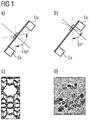
- the chemically leaching of ZSM-5 leads to a cylindrical cavity that runs parallel to the crystallographic c-axis. This provides optical control of the preferred orientation of the crystallites ( Fig. 1d).
- Fig. 1 illustrates that a conventional sample support leads to incomplete data.
- a crystal close to the grid bar reduces the maximum rotation range.
- the dark rim without interruption shows the leached channel parallel to the crystallographic c-axis.
- FIG. 2 schematicalls illustrates a small section of the ZSM-5 framework. Missing wedge data leads to elongated electrostatic potential maps.
- (e) to (h) illustrate the missing volume in reciprocal space. Grey shaded: observed data, white wedge: missing data. Crystallographic b-axis in light grey, c-axis in dark grey.
- ZSM-5 crystals were deposited on a conventional, flat carbon support. Gentle striking of the carbon support with a fine-haired brush caused the carbon film to wrap up ( Fig. 3(a) ). Crystals attached to the carbon film surface, for example by cohesion or adhesion, followed the curvature induced by the soft brushing and thus changed their orientation ( Fig. 3(a) and (b) ). The degree of wrapping per mesh depends on the applied pressure and can be conveniently monitored with a light microscope ( Fig. 3(c) ). The direction of striking provides some control of the direction of the wrapping. Data of nine different crystals were collected. Merging all nine data sets together yielded 100% complete data.
- Figure 3 illustrates the complete data from wrapped carbon grids.
- Plastic fibers in particular nylon fibres
- Nylon fibres with a diameter of about 100 nm were deposited on commercially available carbon grids. This created a chaotic network with open spaces of various diameter ( Fig. 4(a), (b) ). The density was controlled with the deposition duration and thus could be adjusted to the particle size of the investigated crystals: lower density leaves larger holes.
- the size of the ZSM-5 crystals was between 400 and 600 nm.
- the fibrous network and zeolite crystals have more or less matching dimensions. This match of dimensionality can be an important prerequisite for the sample holder.
- a network based on carbon nanotubes is applicable for single particle analysis, but it would appear flat for the large zeolite crystals.
- Fig. 4(c) shows zeolite crystals entangled in the nylon fibre network.
- Figure 4 depicts the complete data from grids coated with 100nm nylon fibres, (a) TEM micrograph of a nylon coated sample support with low fibre density (on top of lacey carbon). (b) TEM micrograph of a nylon coated sample support with mid fibre density. (c) TEM micrograph of a nylon coated sample support with high fibre density. (d) TEM micrograph of ZSM-5 crystals entangled in nylon fibres (on top of lacey carbon). (e) Four data sets reach 100% data completeness. (f) Map calculated from 100% complete data from six crystals results in reliable atom positions (T-O bonds of ZSM-5 shown as bars).
- Imaging and diffraction techniques based on transmission electron microscopes are impeded by incomplete data, as electrons do not penetrate the sample support.
- multiple data sets can be merged to reach complete data.
- most crystals grow with a flat shape and lie on the sample support in preferred orientation. This is ruining the attempt to reach data completeness by merging.
- Plastic fibers such as nylon fibres
- nylon fibres are more reproducible and offer more control: both the fiber diameter and the fiber density can be adjusted to the specimen.
- the concept of nylon fibres is also suitable for sample deposition in a liquid environment and can also be used as a sieve, e.g. for the study of protein crystals in combination with vitrification.
- tomography can benefit from averaging of multiple data sets, the application of these grids may find applications outside the wide field of crystallography.
- ZSM-5 crystals were be prepared as described. Crystals were leached in NaOH solution (0.15 M, 35 ml/g zeolite) at 80°C for 10 h. The product was separated by centrifugation for 15 min at 15,000 rpm, washed three times and dried overnight at 100°C.
- the final gel composition of 0.01 Al 2 O 3 : 1 SiO 2 : 0.25 TPAOH : 0.05 Na 2 : 80 H 2 O and crystallization was performed in a stainless steel autoclave (100 ml). The product was separated by centrifugation for 15 min at 15,000 rpm, washed three times, dried overnight at 100°C and calcined for 10 h at 550°C.
- a nylon nanofiber grid supported by copper TEM grids (Lacey F/C 400 mesh Cu, Ted Pella Inc., USA) was prepared by an electrospinning process. Pellets with 15 wt% of Nylon-6 (particle size 3 mm, Sigma Aldrich, USA) dissolved in formic acid (purum ⁇ 98.0%, Fluka, Germany) and high voltage (20 kV) was applied to the solution through a stainless steel needle on a plastic syringe. A syringe pump (NE-300, New Era Pump Systems Inc., USA) kept feeding the solution to the electrospinning system with 1.5 ⁇ l/min and the TEM grid was placed on the collecting plate made of stainless steel. Electro-spun nylon nanofibers were deposited on the grid for two minutes. The prepared nylon nanofiber grids were dried in the ambient condition for 24 hours.
- the MFI nano crystals were either applied as dispersion (1.5 mg/ ml) or as dust cloud generated by a paintbrush on a commercially available continuous carbon TEM grid (Ted Pella, 01843-F) respectively the nylon grids.
- the continuous carbon TEM grids were plasma-treated before.
- a fine-hair paintbrush was used to wrap up the continuous carbon film on the grids in a controlled way. According process can be observed by eye or targeted folding procedures of single meshes aimed with a light microscope.
- the grids were mounted with the mesh diagonal perpendicular to the rotation axis of the TEM sample holder.
- the read out time of the detector was set to 100 Hz and the data collected in continuous read-out mode at camera lengths of 715 and 495 mm. Resulting datasets were compressed in the HDF5 file format. Integration and optimisation of the data was executed by the program XDS. To control the correct assignment of the a- and b-axis all data sets were solved with direct methods with SHELXT in Laue group mmm. Only the framework atoms Si and O were provided without explicit atom counts. In some cases, SHELXT suggested either of the long unit cell axes as a-axis. In such cases, model refinement was carried out to select the setting with the better R1-value. From thereon, data of MFI crystals was processed without space group constraints, i.e. in Laue group 1 - . Afterwards data was merged by the program XSCALE. The merged datasets again were solved by direct methods with the program SHELXT.
Landscapes
- Chemical & Material Sciences (AREA)
- Analytical Chemistry (AREA)
- Crystallography & Structural Chemistry (AREA)
- Physics & Mathematics (AREA)
- Health & Medical Sciences (AREA)
- Life Sciences & Earth Sciences (AREA)
- Biochemistry (AREA)
- General Health & Medical Sciences (AREA)
- General Physics & Mathematics (AREA)
- Immunology (AREA)
- Pathology (AREA)
- Analysing Materials By The Use Of Radiation (AREA)
Abstract
It is therefore the objective of the present invention to provide a sample support that enables for example sub-micro range crystals to be deposited on the sample support in an arbitrary orientation although the crystals might have a preferred orientation.This objective is achieved according to the present invention by a sample support for samples in the submicron range in imaging and diffraction techniques, comprising a topographically modulated surface; said surface comprising ridge-like and terrace-like structures having dimensions in the order of magnitude to the size of the submicron-sized sample.Therefore, the topographical structure of ridge-like and terrace like section prevents the 3D crystalline probes from the deposition in a preferred direction due to the shape of the crystal structure on the probe support.
Description
- The present invention relates to a sample support for 3D samples in the submicron range for structure investigation by electron transmission systems.
- The ever-growing interest in the atomic structures of submicron-sized crystals has led to the deployment of electron crystallography in transmission electron microscopes. Electron crystallography retrieves in nearly all of the cases incomplete structural data. The reason for this are crystals which shade their complete space from the sampling electrons by a preferred orientation on conventional sample supports. A new method of sample preparation and a new idea for the design of sample supports obstructs this preferred orientation. Thus sampling of the complete space from only very few crystals is enabled. This suggests that electron crystallography may become versatile and for the first time independent of the crystal shape. Moreover the adjustability of the introduced supports might access the complete space of various objects in transmission electron microscopes.
- The overwhelming majority of molecular structures is solved with X-ray crystallography. Electron crystallography solves three-dimensional atomic structures from submicron crystals that are too small for X-rays. The largest drawback of this method is the difficulty to obtain complete datasets that are needed for an accurate structure determination. Most crystals obtain a preferred orientation on a conventional, flat sample support. This systematically shades part of the sample and renders it fruitless to combine data from several crystals to achieve full data completeness.
- Many objects tend to have a preferred orientation. A flat box falls on one of its largest faces and needles do not stand on their tip. This affects material properties of such objects and affects how one can access such objects. Many imaging and diffraction techniques require three-dimensional access to a sample to obtain complete information. Preferred orientation of the sample often makes this impossible. In particular, methods that use electron radiation are particularly affected: The electron beam cannot penetrate the sample support, which is generally much thicker than the sample and which shades the sample from the electron beam. This creates a dead zone with no data, known as the missing wedge problem. Several methods address this problem: In two-dimensional electron crystallography and electron tomography, information of the missing wedge is partly recovered by phase and amplitude extrapolation. Three-dimensional crystals can be shaped by ion beam milling to enforce a different orientation, or they are embedded into a resin that disorders their preferred orientation. Data can also be completed with X-ray powder diffraction in a hybrid method approach. Every method that produces samples in a varying independent orientation makes it possible to combine data from several samples in order to increase completeness. The data quality is improved when the variation in orientation is random. Crystallography is particularly well suited for the combination of different data sets, because determination of the sample orientation is an essential part of data analysis. The correct combination of crystallographic data is well developed. In X-ray crystallography, the crystal is oriented by multi-axis goniometers. Many materials are transparent to X-rays, and shading does not prevent data to be collected from many orientations. In electron diffraction, the situation is very different. The strong interaction of electrons with matter that enables the study of micrometer- and nanometer-sized crystals, prevents electrons from penetrating most common sample supports, except for very few specialized cases. Since sample supports have a flat surface, any crystal with a flat shape and a low symmetry space group is going to result in incomplete datasets, even when data from many crystals are merged. A conventional sample support used in transmission electron microscopes (TEM) is a thin and flat carbon film transparent for electrons. It is stabilized by a copper or gold grid. The grid is non-transparent for electrons. This restricts the maximum available rotation angle to about 140° when the sample is centered between the grid bars. This is further reduced when the crystal lays off-center. The systematic lack of diffraction data leads to a distortion of the calculated electron potential map, which is the basis for the molecular model associated with an increased uncertainty in atom coordinates and atomic displacement parameters.
- It is therefore the objective of the present invention to provide a probe support that enables for example sub-micro range samples to be deposited on the probe support in an arbitrary orientation although the samples might have a preferred orientation.
- This objective is achieved according to the present invention by a sample support for 3D samples in the submicron range in electron microscopy, comprising a topographically modulated surface; said surface comprising ridge-like and terrace-like structures having dimensions in the order of magnitude to the size of the 3D samples.
- Therefore, the topographical structure of ridge-like and terrace like section prevents the samples from the deposition in a preferred direction due to the shape of the crystal structure on the sample support.
- A preferred embodiment can provide for a sample support where the topographically modulated surface is generated by brushing a carbon film having a thickness lower than 1 µm. By varying the pressure and/or the angle of the brushing the generation of the ripples can by controlled in the desired way.
- Preferably, the 3D crystalline samples are distributed over the topographically modulated surface by the brushing. In other words, the 3D crystalline samples are deposited on the carbon layer prior to the brushing with a fine-haired brush and then distributed by the brushing. Coincidently, the samples adhere to the brushed carbon fibers by cohesion.
- Another preferred embodiment can provide for a sample support where the topographically modulated surface is generated by distributing nanotubes and/or nano-cylinders, made for example of carbon and/or plastic, such as nylon, on a support grid, such as a carbon support grid. Typically for the intended use of the sample support, the nanotubes and/or nano-cylinders may have a diameter of 50 to 1000 nm. The density of the deposited nanotubes and/or cylinders was controlled with the deposition duration and thus could be adjusted to the particle size of the investigated crystal samples: lower density leaves larger holes.
- The sample support as explained above can be used in an electron microscope.
- The present invention therefore provides two examples for three-dimensional sample supports that produce complete datasets from only a few crystals. The first type creates the three dimensional sample support by wrapping an ultra-thin carbon layer. The second type is composed of chaotic nylon nano fibers. It is demonstrated that both types break the preferred orientation of MFI-type zeolite nano crystals without reducing data quality. In both cases, less than five crystals are sufficient to achieve complete data. The easy-to-obtain three-dimensional sample supports possess different features with versatile areas of application. Thus, it is anticipated that this kind of sample support will finally give rise to a broad range of complete three-dimensional reconstructions in TEM. This will allow for a more precise view on molecular and atomic structures of functional materials, chemical compounds, and proteins.
- Preferred embodiments of the present invention are hereinafter discussed in more detail with reference to the attached drawings which depict in:
- Fig. 1
- a conventional sample support used in X-ray and electron crystallography;
- Fig. 2
- schematically a small section of the ZSM-5 framework;
- Fig. 3
- the complete data from wrapped carbon grids used as sample support in electron crystallography; and
- Fig. 4
- the complete data from carbon grids coated with 100nm nylon fibres used as sample support in electron crystallography.
- The present invention proposes a simple and generally applicable concept that solves the problem of the 'missing wedge' problem in electron microscopy by introducing sample supports with a three-dimensional structure. One approach wraps up a carbon surface of a thin carbon layer. Crystals to be investigated stick to the curved surface and thus have many different orientations. The second approach covers a sample grid with thin nylon fibres with a diameter similar to the crystal size. This creates a mesh that positions crystals in random orientations. The efficiency of each approach was determined using crystals of ZSM-5, a zeolite of the MFI framework. The habit of ZSM-5 crystals is akin a flat box. The direction of the short crystallographic c-axis coincides with the short macroscopic edge of the crystal. ZSM-5 crystals are therefore an ideal representative of submicron samples affected by preferred orientation. The chemically leaching of ZSM-5 leads to a cylindrical cavity that runs parallel to the crystallographic c-axis. This provides optical control of the preferred orientation of the crystallites (
Fig. 1d). Fig. 1 illustrates that a conventional sample support leads to incomplete data. (a) When the crystal is centered between grid bars, the maximum rotation range is about 140°. (b) A crystal close to the grid bar reduces the maximum rotation range. (c) TEM micrograph of ZSM-5 crystals with preferred orientation. (d) The dark rim without interruption shows the leached channel parallel to the crystallographic c-axis. - The effect of incomplete data is shown in
Figure 2 . With complete data, the electrostatic potential map is spherical centered about the every framework atom (Fig. 2(a) ). Already with 10% data missing, the elongation of the map becomes obvious (Fig. 2 (b-d)). The potential map elongates in the direction of the missing wedge. The elongation increases with increasing volume of the missing wedge.Figure 2 schematicalls illustrates a small section of the ZSM-5 framework. Missing wedge data leads to elongated electrostatic potential maps. (a) complete data. (b) missing wedge with 10° opening, 90% data completeness. (c) Missign wedge with 30° opening, 66% data completeness. (d) Missing wedge with 50° opening, 45% data completeness. (e) to (h) illustrate the missing volume in reciprocal space. Grey shaded: observed data, white wedge: missing data. Crystallographic b-axis in light grey, c-axis in dark grey. - ZSM-5 crystals were deposited on a conventional, flat carbon support. Gentle striking of the carbon support with a fine-haired brush caused the carbon film to wrap up (
Fig. 3(a) ). Crystals attached to the carbon film surface, for example by cohesion or adhesion, followed the curvature induced by the soft brushing and thus changed their orientation (Fig. 3(a) and (b) ). The degree of wrapping per mesh depends on the applied pressure and can be conveniently monitored with a light microscope (Fig. 3(c) ). The direction of striking provides some control of the direction of the wrapping. Data of nine different crystals were collected. Merging all nine data sets together yielded 100% complete data. Subsequently, poorly fitting data sets, judged by the correlation coefficient of intensities between pairs of data sets, were manually excluded from merging as long as this did not reduce the data completeness. This way the number of required data sets could be reduced to only four data sets that yielded 100% complete data (Fig. 3(d) ). A deterioration of the data quality was not observed. For each data set, it was possible to distinguish the crystallographic a-axis from the crystallographic b-axis based on data statistics. -
Figure 3 illustrates the complete data from wrapped carbon grids. (a) STEM micrograph of wrapped carbon with attached ZSM-5 crystals. (b) Cartoon illustrating the randomized orientation. (c) The wrapping is visible with a light microscope. (d) Map calculated from 100% complete data from six crystals results in reliable atom positions (T-O bonds of ZSM-5 shown as bars). - Nylon fibres with a diameter of about 100 nm were deposited on commercially available carbon grids. This created a chaotic network with open spaces of various diameter (
Fig. 4(a), (b) ). The density was controlled with the deposition duration and thus could be adjusted to the particle size of the investigated crystals: lower density leaves larger holes. The size of the ZSM-5 crystals was between 400 and 600 nm. Hence, the fibrous network and zeolite crystals have more or less matching dimensions. This match of dimensionality can be an important prerequisite for the sample holder. A network based on carbon nanotubes is applicable for single particle analysis, but it would appear flat for the large zeolite crystals.Fig. 4(c) shows zeolite crystals entangled in the nylon fibre network. The variation of orientation is less obvious than with the wrapped carbon film. Diffraction data were collected randomly from eight different crystals. The oscillation range for every crystal varied between 115° and 150°. Despite the seemingly lower variation in orientation, complete data was reached by merging diffraction data from four crystals (Fig. 4(d) ). -
Figure 4 depicts the complete data from grids coated with 100nm nylon fibres, (a) TEM micrograph of a nylon coated sample support with low fibre density (on top of lacey carbon). (b) TEM micrograph of a nylon coated sample support with mid fibre density. (c) TEM micrograph of a nylon coated sample support with high fibre density. (d) TEM micrograph of ZSM-5 crystals entangled in nylon fibres (on top of lacey carbon). (e) Four data sets reach 100% data completeness. (f) Map calculated from 100% complete data from six crystals results in reliable atom positions (T-O bonds of ZSM-5 shown as bars). - Imaging and diffraction techniques based on transmission electron microscopes are impeded by incomplete data, as electrons do not penetrate the sample support. In some applications, in particular in crystallography, multiple data sets can be merged to reach complete data. However, most crystals grow with a flat shape and lie on the sample support in preferred orientation. This is ruining the attempt to reach data completeness by merging.
- The general idea of a topographically modulated surface of a probe support and two different types of sample support modification are disclosed herein that lead to a randomisation of the sample orientation and thus to complete data from very few measurements. Both types of sample support are applicable to any samples, both crystalline and non-crystalline, for which 3D structural information are to be obtained through the transmission of electron radiation or electromagnetic radiation like X-rays. Therefore, it will contribute to a deeper understanding of the structure and so the function of many materials. Both types of sample supports are easy to produce and have different properties (see Table 1). This provides a choice depending on the application. Wrapping the carbon layer of the sample support is an easy and fast method. The concept can be further refined through the precise engineering of a sample support, e.g. based on graphene. Plastic fibers, such as nylon fibres, are more reproducible and offer more control: both the fiber diameter and the fiber density can be adjusted to the specimen. The concept of nylon fibres is also suitable for sample deposition in a liquid environment and can also be used as a sieve, e.g. for the study of protein crystals in combination with vitrification. As also tomography can benefit from averaging of multiple data sets, the application of these grids may find applications outside the wide field of crystallography.
- ZSM-5 crystals were be prepared as described. Crystals were leached in NaOH solution (0.15 M, 35 ml/g zeolite) at 80°C for 10 h. The product was separated by centrifugation for 15 min at 15,000 rpm, washed three times and dried overnight at 100°C.
- 12 g tetrapropylammonium hydroxide solution (25 wt% in water) were added to a teflon reactor containing 12.5 g tetraethyl orthosilicate and 77.4 g deionized water. The mixture was heated to 80°C and stirred for 24 h at 500 rpm. After cooling down to room temperature, a solution of sodium hydroxide (0.24 g), aluminum nitrate nonahydrate (0.46 g) and deionized water (4 g) was added dropwise while stirring vigorously. The final gel composition of 0.01 Al2O3: 1 SiO2: 0.25 TPAOH : 0.05 Na2 : 80 H2O and crystallization was performed in a stainless steel autoclave (100 ml). The product was separated by centrifugation for 15 min at 15,000 rpm, washed three times, dried overnight at 100°C and calcined for 10 h at 550°C.
- A nylon nanofiber grid supported by copper TEM grids (Lacey F/C 400 mesh Cu, Ted Pella Inc., USA) was prepared by an electrospinning process. Pellets with 15 wt% of Nylon-6 (particle size 3 mm, Sigma Aldrich, USA) dissolved in formic acid (purum ≥ 98.0%, Fluka, Germany) and high voltage (20 kV) was applied to the solution through a stainless steel needle on a plastic syringe. A syringe pump (NE-300, New Era Pump Systems Inc., USA) kept feeding the solution to the electrospinning system with 1.5 µl/min and the TEM grid was placed on the collecting plate made of stainless steel. Electro-spun nylon nanofibers were deposited on the grid for two minutes. The prepared nylon nanofiber grids were dried in the ambient condition for 24 hours.
- The MFI nano crystals were either applied as dispersion (1.5 mg/ ml) or as dust cloud generated by a paintbrush on a commercially available continuous carbon TEM grid (Ted Pella, 01843-F) respectively the nylon grids. The continuous carbon TEM grids were plasma-treated before. A fine-hair paintbrush was used to wrap up the continuous carbon film on the grids in a controlled way. According process can be observed by eye or targeted folding procedures of single meshes aimed with a light microscope. The grids were mounted with the mesh diagonal perpendicular to the rotation axis of the TEM sample holder.
- Data was collected at room temperature on a Tecnai F30 TEM equipped with a Schottky Emitter at an energy of E=200 keV, i.e. wavelength λ = 0.02508 Å. Dose in TEM Bright field mode was about 0.01 e- Å-2 (the precision of the reading is limited to two digits and displayed 0.00--0.01 e- Å-2. The Goniometer speed was accessed by a hand-written script and operated with a speed of 2.9°/ s. For data acquisition an Eiger X 1M proto-type detector was mounted on the TEM before. The read out time of the detector was set to 100 Hz and the data collected in continuous read-out mode at camera lengths of 715 and 495 mm. Resulting datasets were compressed in the HDF5 file format. Integration and optimisation of the data was executed by the program XDS. To control the correct assignment of the a- and b-axis all data sets were solved with direct methods with SHELXT in Laue group mmm. Only the framework atoms Si and O were provided without explicit atom counts. In some cases, SHELXT suggested either of the long unit cell axes as a-axis. In such cases, model refinement was carried out to select the setting with the better R1-value. From thereon, data of MFI crystals was processed without space group constraints, i.e. in Laue group 1-. Afterwards data was merged by the program XSCALE. The merged datasets again were solved by direct methods with the program SHELXT.
Claims (6)
- A sample support for samples in the submicron range in imaging and diffraction techniques, comprising a topographically modulated surface; said surface comprising ridge-like and terrace-like structures having dimensions in the order of magnitude to the size of the submicron-sized sample.
- The sample support according to claim 1 wherein the topographically modulated surface is generated by brushing a carbon film having a thickness lower than 1 µm.
- The sample support according to claim 2 wherein the 3D crystalline probes are distributed over the topographically modulated surface by the brushing.
- The sample support according to claim 1 wherein the topographically modulated surface is generated by distributing nanotubes and/or nano-cylinders, made for example of carbon and/or plastic, such as nylon, on a support grid, such as a carbon support grid.
- The sample support according to claim 4 wherein the nanotubes and/or nano-cylinders have a diameter of 50 to 1000 nm.
- An electron crystallography system comprising a probe support according to the any of the preceding claims.
Priority Applications (2)
| Application Number | Priority Date | Filing Date | Title |
|---|---|---|---|
| EP18202868.8A EP3644049A1 (en) | 2018-10-26 | 2018-10-26 | Topographically structured support for electron crystallography |
| PCT/EP2019/078145 WO2020083730A1 (en) | 2018-10-26 | 2019-10-17 | Topographically structured support for electron crystallography |
Applications Claiming Priority (1)
| Application Number | Priority Date | Filing Date | Title |
|---|---|---|---|
| EP18202868.8A EP3644049A1 (en) | 2018-10-26 | 2018-10-26 | Topographically structured support for electron crystallography |
Publications (1)
| Publication Number | Publication Date |
|---|---|
| EP3644049A1 true EP3644049A1 (en) | 2020-04-29 |
Family
ID=64082887
Family Applications (1)
| Application Number | Title | Priority Date | Filing Date |
|---|---|---|---|
| EP18202868.8A Withdrawn EP3644049A1 (en) | 2018-10-26 | 2018-10-26 | Topographically structured support for electron crystallography |
Country Status (2)
| Country | Link |
|---|---|
| EP (1) | EP3644049A1 (en) |
| WO (1) | WO2020083730A1 (en) |
Citations (2)
| Publication number | Priority date | Publication date | Assignee | Title |
|---|---|---|---|---|
| US20080237464A1 (en) * | 2007-03-30 | 2008-10-02 | Tsinghua University | Transmission electron microscope micro-grid and method for making the same |
| US20110252619A1 (en) * | 2010-04-14 | 2011-10-20 | Beijing Funate Innovation Technology Co., Ltd. | Method for manufacturing transmission electron microscope micro-grid |
-
2018
- 2018-10-26 EP EP18202868.8A patent/EP3644049A1/en not_active Withdrawn
-
2019
- 2019-10-17 WO PCT/EP2019/078145 patent/WO2020083730A1/en not_active Ceased
Patent Citations (2)
| Publication number | Priority date | Publication date | Assignee | Title |
|---|---|---|---|---|
| US20080237464A1 (en) * | 2007-03-30 | 2008-10-02 | Tsinghua University | Transmission electron microscope micro-grid and method for making the same |
| US20110252619A1 (en) * | 2010-04-14 | 2011-10-20 | Beijing Funate Innovation Technology Co., Ltd. | Method for manufacturing transmission electron microscope micro-grid |
Also Published As
| Publication number | Publication date |
|---|---|
| WO2020083730A1 (en) | 2020-04-30 |
Similar Documents
| Publication | Publication Date | Title |
|---|---|---|
| Lyu et al. | Electron microscopy studies of soft nanomaterials | |
| Szewczyk et al. | Enhanced piezoelectricity of electrospun polyvinylidene fluoride fibers for energy harvesting | |
| Gruene et al. | 3D electron diffraction for chemical analysis: Instrumentation developments and innovative applications | |
| Lv et al. | Low-dose electron microscopy imaging of electron beam-sensitive crystalline materials | |
| Kobayashi et al. | High-resolution TEM images of zinc phthalocyanine polymorphs in thin films | |
| Olszta et al. | Nanofibrous calcite synthesized via a solution− precursor− solid mechanism | |
| Ogawa et al. | Transmission electron microscopy of cellulose. Part 2: technical and practical aspects | |
| Lolla et al. | Polyvinylidene fluoride molecules in nanofibers, imaged at atomic scale by aberration corrected electron microscopy | |
| Griesshaber et al. | Homoepitaxial meso-and microscale crystal co-orientation and organic matrix network structure in Mytilus edulis nacre and calcite | |
| Kim et al. | The cellulose system in the cell wall ofMicrasterias | |
| EP3508622A1 (en) | Nanofiber-nanowire composite and preparation method therefor | |
| Onuma et al. | Artificial enamel induced by phase transformation of amorphous nanoparticles | |
| Wennmacher et al. | 3D-structured supports create complete data sets for electron crystallography | |
| Bourgeois et al. | Boron nitride cones: structure determination by transmission electron microscopy | |
| Khalifa et al. | Mineral and matrix components of the operculum and shell of the barnacle Balanus amphitrite: calcite crystal growth in a hydrogel | |
| EP3644049A1 (en) | Topographically structured support for electron crystallography | |
| KR101222019B1 (en) | Graphene-biomineral hybrid films and preparing method thereof | |
| Dong et al. | Biogenic synthesis of tubular SnO2 with hierarchical intertextures by an aqueous technique involving glycoprotein | |
| CN106841257A (en) | A kind of analysis method of single nanometer materials section stress | |
| Gilis et al. | Morphology, microstructure, crystallography, and chemistry of distinct C a CO 3 deposits formed by early recruits of the scleractinian coral P ocillopora damicornis | |
| RU2845833C1 (en) | Method of producing biocompatible biodegradable polymer piezoactive and magnetoelectric particles | |
| WO2011050518A1 (en) | Method for nanometer textile identification | |
| Koch et al. | Synchrotron radiation studies of non-crystalline systems | |
| Armbruster et al. | H2O ordering and superstructures in armenite, BaCa2Al6Si9O30· 2H2O: A single-crystal X-ray and TEM study | |
| Luo et al. | In situ phosphorus K-edge X-ray absorption spectroscopy studies of calcium–phosphate formation and transformation on the surface of bacterial cellulose nanofibers |
Legal Events
| Date | Code | Title | Description |
|---|---|---|---|
| PUAI | Public reference made under article 153(3) epc to a published international application that has entered the european phase |
Free format text: ORIGINAL CODE: 0009012 |
|
| STAA | Information on the status of an ep patent application or granted ep patent |
Free format text: STATUS: THE APPLICATION HAS BEEN PUBLISHED |
|
| AK | Designated contracting states |
Kind code of ref document: A1 Designated state(s): AL AT BE BG CH CY CZ DE DK EE ES FI FR GB GR HR HU IE IS IT LI LT LU LV MC MK MT NL NO PL PT RO RS SE SI SK SM TR |
|
| AX | Request for extension of the european patent |
Extension state: BA ME |
|
| STAA | Information on the status of an ep patent application or granted ep patent |
Free format text: STATUS: THE APPLICATION IS DEEMED TO BE WITHDRAWN |
|
| 18D | Application deemed to be withdrawn |
Effective date: 20201030 |