EP3642852B1 - Vacuum compatible electrical insulator - Google Patents
Vacuum compatible electrical insulator Download PDFInfo
- Publication number
- EP3642852B1 EP3642852B1 EP18820351.7A EP18820351A EP3642852B1 EP 3642852 B1 EP3642852 B1 EP 3642852B1 EP 18820351 A EP18820351 A EP 18820351A EP 3642852 B1 EP3642852 B1 EP 3642852B1
- Authority
- EP
- European Patent Office
- Prior art keywords
- glass substrate
- electrical insulator
- uncoated
- plasma
- glass
- Prior art date
- Legal status (The legal status is an assumption and is not a legal conclusion. Google has not performed a legal analysis and makes no representation as to the accuracy of the status listed.)
- Active
Links
Images


Classifications
-
- C—CHEMISTRY; METALLURGY
- C03—GLASS; MINERAL OR SLAG WOOL
- C03C—CHEMICAL COMPOSITION OF GLASSES, GLAZES OR VITREOUS ENAMELS; SURFACE TREATMENT OF GLASS; SURFACE TREATMENT OF FIBRES OR FILAMENTS MADE FROM GLASS, MINERALS OR SLAGS; JOINING GLASS TO GLASS OR OTHER MATERIALS
- C03C17/00—Surface treatment of glass, not in the form of fibres or filaments, by coating
- C03C17/22—Surface treatment of glass, not in the form of fibres or filaments, by coating with other inorganic material
- C03C17/23—Oxides
-
- H—ELECTRICITY
- H01—ELECTRIC ELEMENTS
- H01B—CABLES; CONDUCTORS; INSULATORS; SELECTION OF MATERIALS FOR THEIR CONDUCTIVE, INSULATING OR DIELECTRIC PROPERTIES
- H01B3/00—Insulators or insulating bodies characterised by the insulating materials; Selection of materials for their insulating or dielectric properties
- H01B3/02—Insulators or insulating bodies characterised by the insulating materials; Selection of materials for their insulating or dielectric properties mainly consisting of inorganic substances
- H01B3/08—Insulators or insulating bodies characterised by the insulating materials; Selection of materials for their insulating or dielectric properties mainly consisting of inorganic substances quartz; glass; glass wool; slag wool; vitreous enamels
-
- H—ELECTRICITY
- H01—ELECTRIC ELEMENTS
- H01B—CABLES; CONDUCTORS; INSULATORS; SELECTION OF MATERIALS FOR THEIR CONDUCTIVE, INSULATING OR DIELECTRIC PROPERTIES
- H01B3/00—Insulators or insulating bodies characterised by the insulating materials; Selection of materials for their insulating or dielectric properties
- H01B3/02—Insulators or insulating bodies characterised by the insulating materials; Selection of materials for their insulating or dielectric properties mainly consisting of inorganic substances
- H01B3/12—Insulators or insulating bodies characterised by the insulating materials; Selection of materials for their insulating or dielectric properties mainly consisting of inorganic substances ceramics
-
- H—ELECTRICITY
- H01—ELECTRIC ELEMENTS
- H01B—CABLES; CONDUCTORS; INSULATORS; SELECTION OF MATERIALS FOR THEIR CONDUCTIVE, INSULATING OR DIELECTRIC PROPERTIES
- H01B17/00—Insulators or insulating bodies characterised by their form
- H01B17/56—Insulating bodies
-
- H—ELECTRICITY
- H01—ELECTRIC ELEMENTS
- H01J—ELECTRIC DISCHARGE TUBES OR DISCHARGE LAMPS
- H01J37/00—Discharge tubes with provision for introducing objects or material to be exposed to the discharge, e.g. for the purpose of examination or processing thereof
- H01J37/32—Gas-filled discharge tubes
-
- C—CHEMISTRY; METALLURGY
- C03—GLASS; MINERAL OR SLAG WOOL
- C03C—CHEMICAL COMPOSITION OF GLASSES, GLAZES OR VITREOUS ENAMELS; SURFACE TREATMENT OF GLASS; SURFACE TREATMENT OF FIBRES OR FILAMENTS MADE FROM GLASS, MINERALS OR SLAGS; JOINING GLASS TO GLASS OR OTHER MATERIALS
- C03C2217/00—Coatings on glass
- C03C2217/20—Materials for coating a single layer on glass
- C03C2217/21—Oxides
- C03C2217/214—Al2O3
-
- C—CHEMISTRY; METALLURGY
- C03—GLASS; MINERAL OR SLAG WOOL
- C03C—CHEMICAL COMPOSITION OF GLASSES, GLAZES OR VITREOUS ENAMELS; SURFACE TREATMENT OF GLASS; SURFACE TREATMENT OF FIBRES OR FILAMENTS MADE FROM GLASS, MINERALS OR SLAGS; JOINING GLASS TO GLASS OR OTHER MATERIALS
- C03C2217/00—Coatings on glass
- C03C2217/20—Materials for coating a single layer on glass
- C03C2217/21—Oxides
- C03C2217/228—Other specific oxides
-
- H—ELECTRICITY
- H05—ELECTRIC TECHNIQUES NOT OTHERWISE PROVIDED FOR
- H05H—PLASMA TECHNIQUE; PRODUCTION OF ACCELERATED ELECTRICALLY-CHARGED PARTICLES OR OF NEUTRONS; PRODUCTION OR ACCELERATION OF NEUTRAL MOLECULAR OR ATOMIC BEAMS
- H05H1/00—Generating plasma; Handling plasma
- H05H1/24—Generating plasma
- H05H1/46—Generating plasma using applied electromagnetic fields, e.g. high frequency or microwave energy
Definitions
- the present disclosure generally relates to a vacuum compatible electrical insulator.
- Electrical insulators are well known in the art Electrical insulators are used in electrical equipment to support and separate electrical conductors without allowing current flow through the insulator itself. All electrical insulators become electrically conductive when a sufficiently large voltage is applied and the electric field tears electrons away from the atoms of the insulator (known as "breakdown voltage" of the insulator). An electrical insulator is typically used in high energy plasma systems, charged particle accelerators or high-voltage generators. In some applications, electrical insulators need to be vacuum compatible (e.g. when installed as part of a vacuum vessel), such as the electrical insulators must hold a voltage across the insulator's surface without breaking down while maintaining vacuum conditions.
- Electrical insulators used in a vacuum are prone to breakdown across surfaces of the insulator at voltages which are much lower than the voltages required to cause breakdown through the material itself when in an air atmosphere.
- the electrical insulator needs to withstand exposure to high energy ionized plasma that may contact the surface of the insulator, without damaging such surface.
- the most common materials for vacuum compatible electrical insulators are ceramics, such as alumina (Al 2 O 3 ).
- Alumina used as an insulator is vacuum compatible and can sustain voltages across its surface without breakdown; however, manufacturing a large size ceramic insulator can be challenging.
- the largest known commercially available alumina insulator is about 1 meter in diameter. The problem with making large alumina components is that it can fracture easily during the manufacturing process. As a result, the manufacture of large size alumina insulators is a complex and expensive process.
- Some known solutions for providing a large size alumina insulator include using multiple small alumina tiles in place of one large insulator, but this adds additional complexity to the instalment of the insulator and can compromise the vacuum quality.
- Glass can be made to very large sizes and is a good electrical insulator; however, it is easily damaged by exposure to charged particles (e.g. plasma) and under vacuum the charge buildup along the glass surface may trigger a surface flashover due to high surface resistivity of the glass. The charged particles can damage the glass surface and cause the insulator to fail and/or significantly reduce the hold-off voltage that needs to be maintained across the insulator's surface.
- charged particles e.g. plasma
- Plastic is also often used as an electrical insulator material.
- Plastic electrical insulators can be made to very large size, but are not compatible with vacuum applications (outgassing is too high) and are easily broken down with exposure to charged particles.
- a vacuum compatible electrical insulator comprises a glass substrate having at least one face surface with at least a portion exposable to high energy charged particles or photons, and a ceramic layer coating the at least one portion of the at least one face surface of the glass substrate.
- the glass substrate may be a single piece of glass that is circular and has a diameter of at least 1 m.
- the glass substrate may be composed of borosilicate glass.
- the ceramic layer can be composed of a material selected from a group consisting of yttria and alumina.
- a plasma system comprises a vacuum vessel, a first electrode and a second electrode mount in the vacuum vessel and spaced apart to form a gap therein between such that a voltage can be applied between the first and the second electrodes and an electrical insulator mounted between the two electrodes.
- the electrical insulator comprises a glass substrate with at least one face surface with at least a portion exposable to plasma inside the vacuum vessel and a ceramic layer coating the at least one portion of the at least one face surface.
- Embodiments of the invention described herein relate to an electrical insulator suitable for use in large size and vacuum applications.
- the electrical insulator is suitable for use in plasma generating systems and particles accelerators, wherein the insulator is placed in a gap between the electrodes.
- the electrical insulator may have a diameter of about ⁇ 2 meters or larger.
- the largest commercially available ceramic (e.g. alumina) insulator is about 1 meter in diameter and the cost for manufacturing such large alumina insulators is several hundred thousand dollars per piece.
- it is expected that embodiments of the electrical insulator are simpler and less expensive to manufacture.
- Embodiments of the electrical insulator disclosed herein can be installed in a vacuum vessel, are designed to be quite large (not limited by size) and are able to withstand exposure to high energy charged particles, such as plasma.
- Embodiments of the invention are described herein in use with respect to a plasma generation system.
- a plasma generation system for instance, x-ray systems, electron tubes, beam injectors, particle accelerators or other devices that require electrical insulators.
- the discussion of the plasma generation system herein below is merely an example of one such implementation and is not intended to be limiting in terms of modality. Persons skilled in the art would understand that the invention is applicable for other systems that require installation of an electrical insulator that operates under vacuum.
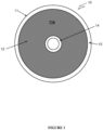
- FIG. 1 illustrates an example of an electrical insulator 10 that comprises a glass (SiO 2 ) substrate 11 and a ceramic coating layer 12.
- the glass substrate 11 comprises a body that can act as a vacuum seal between the high vacuum and the external atmosphere.
- the glass substrate 11 can be composed of a borosilicate glass.
- the glass substrate 11 can be cut out of a single piece of glass and can have a pre-determined desired size and shape.
- the illustrated example of the glass substrate 11 has a ring shape (e.g. a disk).
- the glass substrate 11 has at least one face surface 11a that is coated with the ceramic layer 12.
- the face surface 11a is a surface of the insulator that is exposed to the high energy charged particles.
- the ceramic coating layer 12 is configured to protect the glass substrate 11 from being damaged by high energy charged particles or photons while still holding the voltages under vacuum.
- the ceramic coating 12 is applied to the face surface 11a and it should be thick enough to sustain the voltages and the exposure to charged particles in order to protect the glass substrate 11.
- the ceramic coating layer 12 can be 10 ⁇ m - 200 ⁇ m thick coating the face surface 11a.
- the ceramic coating layer can be a different thickness in other embodiments.
- Any suitable coating process can be used to apply the coating layer 12.
- the ceramic coating layer 12 can be applied to the glass substrate 11 using a plasma spray deposition, vapor deposition or any other suitable deposition process that can be used to apply a ceramic coating on a glass substrate.
- the coating layer 12 can be, for example, an alumina (Al 2 O 3 ) or any other ceramic material known to be suitable for use in vacuum and plasma environments.
- the coating layer 12 can be yttria (yttrium (III) oxide Y 2 O 3 .
- the glass substrate can have a cylindrical, rectangular, tubular or any other desired shape or combination thereof.
- the surface of the glass substrate 11 can comprises a number of folds to compensate for difference between the coefficient of thermal expansion of the glass substrate 11 (e.g. borosilicate glass) and the coefficient of thermal expansion of the ceramic coating 12 (e.g. alumina, yttria).
- the ceramic coating 12 is applied only on one side of the substrate 11, because only one side of the insulator faces and is exposed to the vacuum/plasma; however person skilled in the art would understand that both sides (and/or edges) of the insulator 10 can be coated with the ceramic layer 12 without departing from the scope of the invention.
- the face surface 11a can be a continuous single surface or comprise multiple surface portions.
- the face surface 11a can comprise multiple surface portions when the insulator 10 is used in applications where only parts of the insulator 10 is exposed to high energy changed particles; in such applications, two or more coated face surface portions 11a are interspersed with one or more uncoated surface portions (not shown).
- the electrical insulator 10, illustrated in FIG 1 can have an uncoated region 14 around an inner diameter and an uncoated region 15 around an outer circumference of the electrical insulator 10.
- the uncoated regions 14 and 15 can be used as seats for seal(s), such as for example O-ring seals, that can be mounted against the uncoated glass regions 14, 15, so that the electrical insulator 10 can form a vacuum seal and an electrically insulating barrier between the two conductors.
- the ceramic coating layer 12 maintains the electrically insulating barrier between the electrodes and withstands exposure to the high energy ionized plasma.
- the alumina coating layer 12 protects the glass substrate 11 from being damaged by the plasma and it maintains its electrically insulating properties when it is exposed to the plasma.
- the vacuum seal could also be made through a metal interface ring that is bonded to the glass.
- the uncoated glass regions could be metallized using any standard method to deposit metal on to a glass substrate.
- the metallized region of the glass could then be leak tight bonded to a suitable low thermal expansion metal (such as for example Invar).
- FIG. 2 illustrates a schematic of an example of a plasma system 40 using the ceramic coated glass electrical insulator 10.
- the plasma generation system 40 is configured to generate plasma and it comprises a plasma generation vessel 41 with a first 46 and a second electrode 47.
- the plasma system 40 is evacuated using a pumping system 44.
- the ceramic coated glass electrical insulator 10 is mounted in proximity to a close end 42 of the vessel 41, such that a face surface 10a of a glass substrate 10b faces the inner cavity 45.
- the face surface 10a is coated with a ceramic layer (e.g. alumina), so that the alumina layer covers the face surface 10a of the glass substrate 10b.
- a ceramic layer e.g. alumina
- a number of gas valves 43 can be used to symmetrically inject a precise quantity of gas into an annular gap 48 formed between the electrodes 46 and 47.
- the plasma system 40 can further comprise a power source 52 configured to provide a discharge pulse to the first electrode 46 so that a current flows across the gap 48 between the electrodes 46 and 47, ionizing the gas and forming plasma.
- the electrical insulator 10 separates the electrodes 46 and 47 and forms an electrically insulating barrier therein between.
- the electrical insulator 10 illustrated in FIG. 2 has a disk (ring) shape with diameter of 1 m or larger.
- the electrical insulator 10 can have other shapes depending on the position and relationship of the two electrodes.
- the ceramic coated glass electrical insulator has been tested in a number of plasma systems at General Fusion Inc.
- the ceramic coated glass electrical insulator was installed between an inner electrode and a ground potential electrode.
- the ceramic coated glass electrical insulator comprised an annular discshaped glass substrate composed of borosilicate glass and having an outer diameter of 14 inches (35.56 cm), an inner diameter of 4" (-10.16 cm) and a thickness of 0.75" (-1.9 cm).
- the ceramic layer coating the glass substrate was composed of alumina, had a thickness of about 100 ⁇ m and was applied on the glass substrate by a plasma spray method.
- a vacuum vessel was used as the ground potential electrode for the plasma discharge. O-ring seals were used to seal the vacuum vessel.
- a voltage of about 20kV was applied across the ceramic-coated glass electrical insulator for 50 - 100 ⁇ s per pulse for hundreds of pulses.
- the ceramic-coated glass electrical insulator was further exposed to plasma that was generated between the electrodes.
- the same test was conducted using an uncoated (bare) glass insulator (see FIG. 4 ) having the same composition and dimensions as the glass substrate of the ceramic coated glass electrical insulator. Results are shown in FIGs. 3 and 4 .
- the tests with the ceramic coated glass electrical insulator show a slight discoloration on the coating (most probably contamination from the vacuum chamber); however, no significant damage of the electrical insulator's surface occurred and the electrical insulator withstood the voltage pulses and the plasma exposure.
- the contamination did not stop the coating from maintaining its electrically insulating properties.
- the results show that the ceramic coated glass electrical insulator performs as well as any solid ceramic electrical insulator when exposed to plasma discharges; however the cost for manufacturing a big ceramic coated glass insulator is expected to be much lower than manufacturing a large solid ceramic (alumina) insulator.
- the coating was also applied to a glass substrate shaped as an elongated rod and tested. One electrode was clamped on one end of the coated glass rod and the other electrode was clamped on the opposite end of the glass rod.
- the assembly of the electrodes with the insulator between the electrodes was put in a vacuum chamber and a voltage ( ⁇ 30kV) was applied between the electrodes. A helium gas was injected into the vacuum chamber to initiate a breakdown between the electrodes and to generate plasma.
- the ceramic coating was applied around the circumference of the glass rod forming a coating layer on the face surface of the insulator. In the tests conducted with the coated glass rod insulators, the insulators were able to withstand repeated breakdowns without significant damage or loss of ability to hold off voltage.
Landscapes
- Chemical & Material Sciences (AREA)
- Engineering & Computer Science (AREA)
- Inorganic Chemistry (AREA)
- Physics & Mathematics (AREA)
- Ceramic Engineering (AREA)
- Plasma & Fusion (AREA)
- Chemical Kinetics & Catalysis (AREA)
- Life Sciences & Earth Sciences (AREA)
- Materials Engineering (AREA)
- Organic Chemistry (AREA)
- General Chemical & Material Sciences (AREA)
- Geochemistry & Mineralogy (AREA)
- Spectroscopy & Molecular Physics (AREA)
- Electromagnetism (AREA)
- Analytical Chemistry (AREA)
- Electron Sources, Ion Sources (AREA)
- Plasma Technology (AREA)
- Surface Treatment Of Glass (AREA)
- Inorganic Insulating Materials (AREA)
- Insulating Bodies (AREA)
- Drying Of Semiconductors (AREA)
- Physical Vapour Deposition (AREA)
Description
- The present disclosure generally relates to a vacuum compatible electrical insulator.
- Electrical insulators are well known in the art Electrical insulators are used in electrical equipment to support and separate electrical conductors without allowing current flow through the insulator itself. All electrical insulators become electrically conductive when a sufficiently large voltage is applied and the electric field tears electrons away from the atoms of the insulator (known as "breakdown voltage" of the insulator). An electrical insulator is typically used in high energy plasma systems, charged particle accelerators or high-voltage generators. In some applications, electrical insulators need to be vacuum compatible (e.g. when installed as part of a vacuum vessel), such as the electrical insulators must hold a voltage across the insulator's surface without breaking down while maintaining vacuum conditions. Electrical insulators used in a vacuum are prone to breakdown across surfaces of the insulator at voltages which are much lower than the voltages required to cause breakdown through the material itself when in an air atmosphere. In addition, for some applications (e.g. plasma systems), the electrical insulator needs to withstand exposure to high energy ionized plasma that may contact the surface of the insulator, without damaging such surface.
- The most common materials for vacuum compatible electrical insulators are ceramics, such as alumina (Al2O3). Alumina used as an insulator is vacuum compatible and can sustain voltages across its surface without breakdown; however, manufacturing a large size ceramic insulator can be challenging. The largest known commercially available alumina insulator is about 1 meter in diameter. The problem with making large alumina components is that it can fracture easily during the manufacturing process. As a result, the manufacture of large size alumina insulators is a complex and expensive process. Some known solutions for providing a large size alumina insulator include using multiple small alumina tiles in place of one large insulator, but this adds additional complexity to the instalment of the insulator and can compromise the vacuum quality.
- Another common electrical insulator material is glass (SiO2). Glass can be made to very large sizes and is a good electrical insulator; however, it is easily damaged by exposure to charged particles (e.g. plasma) and under vacuum the charge buildup along the glass surface may trigger a surface flashover due to high surface resistivity of the glass. The charged particles can damage the glass surface and cause the insulator to fail and/or significantly reduce the hold-off voltage that needs to be maintained across the insulator's surface.
- Plastic is also often used as an electrical insulator material. Plastic electrical insulators can be made to very large size, but are not compatible with vacuum applications (outgassing is too high) and are easily broken down with exposure to charged particles.
- Cited prior art includes:
-
US 6 734 629 82 (PATENT TREUHAND GES FUER ELEKTRISCHE GLUEHLAMPEN M8H [DE]); - SZCZEKLIK J ET AL: "Kinetics of the formation of thin films of aluminium oxide in a low temperature plasma", THIN SOLID FILMS, ELSEVIER, AMSTERDAM, NL, vol. 71, no. 1, 15 August 1980 (1980-08-15), pages L17-L19, XP025720065, ISSN: 0040-6090;
-
EP 0 963 015 A2 (CYMER INC [US]) ; -
US 6 331 194 81 (SAMPAYAN STEPHEN E [US] ET AL ) - Aspects of the invention are set out in the appended independent claims. A vacuum compatible electrical insulator is provided. The vacuum compatible electrical insulator comprises a glass substrate having at least one face surface with at least a portion exposable to high energy charged particles or photons, and a ceramic layer coating the at least one portion of the at least one face surface of the glass substrate.
- The glass substrate may be a single piece of glass that is circular and has a diameter of at least 1 m.
- The glass substrate may be composed of borosilicate glass. The ceramic layer can be composed of a material selected from a group consisting of yttria and alumina.
- A plasma system is provided. The plasma system comprises a vacuum vessel, a first electrode and a second electrode mount in the vacuum vessel and spaced apart to form a gap therein between such that a voltage can be applied between the first and the second electrodes and an electrical insulator mounted between the two electrodes. The electrical insulator comprises a glass substrate with at least one face surface with at least a portion exposable to plasma inside the vacuum vessel and a ceramic layer coating the at least one portion of the at least one face surface.
- Throughout the drawings, reference numbers may be re-used to indicate correspondence between referenced elements. The drawings are provided to illustrate example embodiments described herein and are not intended to limit the scope of the disclosure. Sizes and relative positions of elements in the drawings are not necessarily drawn to scale. For example, the shapes of various elements and angles are not drawn to scale, and some of these elements are arbitrarily enlarged and positioned to improve drawing legibility.
-
FIG.1 is a schematic top view of an example of a high-voltage, vacuum compatible, ceramic coated glass electrical insulator. -
FIG. 2 is a schematic cross-sectional view of a plasma generator with the ceramic coated glass electrical insulator installed in a gap between an inner electrode and an outer electrode. -
FIG. 3a is a photo of an experimental ceramic coated glass electrical insulator after being tested under high voltage, high vacuum and plasma exposure. -
FIG. 3b is a close up photo of the coating of the electrical insulator ofFIG. 3a . -
FIG. 4 is a photo of a bare glass side of an uncoated electrical insulator after being tested under high voltage, high vacuum and plasma exposure. - Embodiments of the invention described herein relate to an electrical insulator suitable for use in large size and vacuum applications. In some embodiments, the electrical insulator is suitable for use in plasma generating systems and particles accelerators, wherein the insulator is placed in a gap between the electrodes. In some embodiments, the electrical insulator may have a diameter of about ~ 2 meters or larger. The largest commercially available ceramic (e.g. alumina) insulator is about 1 meter in diameter and the cost for manufacturing such large alumina insulators is several hundred thousand dollars per piece. In contrast, it is expected that embodiments of the electrical insulator are simpler and less expensive to manufacture.
- Embodiments of the electrical insulator disclosed herein can be installed in a vacuum vessel, are designed to be quite large (not limited by size) and are able to withstand exposure to high energy charged particles, such as plasma.
- Embodiments of the invention are described herein in use with respect to a plasma generation system. However, one skilled in the art will recognize that other embodiments of the invention may be used in other applications, for instance, x-ray systems, electron tubes, beam injectors, particle accelerators or other devices that require electrical insulators. The discussion of the plasma generation system herein below is merely an example of one such implementation and is not intended to be limiting in terms of modality. Persons skilled in the art would understand that the invention is applicable for other systems that require installation of an electrical insulator that operates under vacuum.
-
FIG. 1 illustrates an example of anelectrical insulator 10 that comprises a glass (SiO2)substrate 11 and aceramic coating layer 12. Theglass substrate 11 comprises a body that can act as a vacuum seal between the high vacuum and the external atmosphere. In some implementations, theglass substrate 11 can be composed of a borosilicate glass. Theglass substrate 11 can be cut out of a single piece of glass and can have a pre-determined desired size and shape. For example, the illustrated example of theglass substrate 11 has a ring shape (e.g. a disk). Theglass substrate 11 has at least oneface surface 11a that is coated with theceramic layer 12. Theface surface 11a is a surface of the insulator that is exposed to the high energy charged particles. Theceramic coating layer 12 is configured to protect theglass substrate 11 from being damaged by high energy charged particles or photons while still holding the voltages under vacuum. Theceramic coating 12 is applied to theface surface 11a and it should be thick enough to sustain the voltages and the exposure to charged particles in order to protect theglass substrate 11. In some embodiments, theceramic coating layer 12 can be 10 µm - 200 µm thick coating theface surface 11a. However, persons skilled in the art would understand that the ceramic coating layer can be a different thickness in other embodiments. Any suitable coating process can be used to apply thecoating layer 12. For example, theceramic coating layer 12 can be applied to theglass substrate 11 using a plasma spray deposition, vapor deposition or any other suitable deposition process that can be used to apply a ceramic coating on a glass substrate. Thecoating layer 12 can be, for example, an alumina (Al2O3) or any other ceramic material known to be suitable for use in vacuum and plasma environments. In one implementation, thecoating layer 12 can be yttria (yttrium (III) oxide Y2O3. The glass substrate can have a cylindrical, rectangular, tubular or any other desired shape or combination thereof. In one embodiment, the surface of theglass substrate 11 can comprises a number of folds to compensate for difference between the coefficient of thermal expansion of the glass substrate 11 (e.g. borosilicate glass) and the coefficient of thermal expansion of the ceramic coating 12 (e.g. alumina, yttria). - In the illustrated example of the
insulator 10, theceramic coating 12 is applied only on one side of thesubstrate 11, because only one side of the insulator faces and is exposed to the vacuum/plasma; however person skilled in the art would understand that both sides (and/or edges) of theinsulator 10 can be coated with theceramic layer 12 without departing from the scope of the invention. Theface surface 11a can be a continuous single surface or comprise multiple surface portions. For example, theface surface 11a can comprise multiple surface portions when theinsulator 10 is used in applications where only parts of theinsulator 10 is exposed to high energy changed particles; in such applications, two or more coatedface surface portions 11a are interspersed with one or more uncoated surface portions (not shown). Theelectrical insulator 10, illustrated inFIG 1 , can have anuncoated region 14 around an inner diameter and anuncoated region 15 around an outer circumference of theelectrical insulator 10. Theuncoated regions uncoated glass regions electrical insulator 10 can form a vacuum seal and an electrically insulating barrier between the two conductors. Theceramic coating layer 12 maintains the electrically insulating barrier between the electrodes and withstands exposure to the high energy ionized plasma. For example, thealumina coating layer 12 protects theglass substrate 11 from being damaged by the plasma and it maintains its electrically insulating properties when it is exposed to the plasma. The vacuum seal could also be made through a metal interface ring that is bonded to the glass. The uncoated glass regions could be metallized using any standard method to deposit metal on to a glass substrate. The metallized region of the glass could then be leak tight bonded to a suitable low thermal expansion metal (such as for example Invar). -
FIG. 2 illustrates a schematic of an example of aplasma system 40 using the ceramic coated glasselectrical insulator 10. Theplasma generation system 40 is configured to generate plasma and it comprises aplasma generation vessel 41 with a first 46 and asecond electrode 47. Theplasma system 40 is evacuated using apumping system 44. The ceramic coated glasselectrical insulator 10 is mounted in proximity to aclose end 42 of thevessel 41, such that aface surface 10a of aglass substrate 10b faces theinner cavity 45. Theface surface 10a is coated with a ceramic layer (e.g. alumina), so that the alumina layer covers theface surface 10a of theglass substrate 10b. A number ofgas valves 43 can be used to symmetrically inject a precise quantity of gas into anannular gap 48 formed between theelectrodes plasma system 40 can further comprise apower source 52 configured to provide a discharge pulse to thefirst electrode 46 so that a current flows across thegap 48 between theelectrodes electrical insulator 10 separates theelectrodes electrical insulator 10 illustrated inFIG. 2 has a disk (ring) shape with diameter of 1 m or larger. Theelectrical insulator 10 can have other shapes depending on the position and relationship of the two electrodes. - The ceramic coated glass electrical insulator has been tested in a number of plasma systems at General Fusion Inc. The ceramic coated glass electrical insulator was installed between an inner electrode and a ground potential electrode. The ceramic coated glass electrical insulator comprised an annular discshaped glass substrate composed of borosilicate glass and having an outer diameter of 14 inches (35.56 cm), an inner diameter of 4" (-10.16 cm) and a thickness of 0.75" (-1.9 cm). The ceramic layer coating the glass substrate was composed of alumina, had a thickness of about 100 µm and was applied on the glass substrate by a plasma spray method. A vacuum vessel was used as the ground potential electrode for the plasma discharge. O-ring seals were used to seal the vacuum vessel. A voltage of about 20kV was applied across the ceramic-coated glass electrical insulator for 50 - 100 µs per pulse for hundreds of pulses. The ceramic-coated glass electrical insulator was further exposed to plasma that was generated between the electrodes. The same test was conducted using an uncoated (bare) glass insulator (see
FIG. 4 ) having the same composition and dimensions as the glass substrate of the ceramic coated glass electrical insulator. Results are shown inFIGs. 3 and 4 . The tests with the ceramic coated glass electrical insulator (FIGs. 3a, 3b ) show a slight discoloration on the coating (most probably contamination from the vacuum chamber); however, no significant damage of the electrical insulator's surface occurred and the electrical insulator withstood the voltage pulses and the plasma exposure. The contamination did not stop the coating from maintaining its electrically insulating properties. The results show that the ceramic coated glass electrical insulator performs as well as any solid ceramic electrical insulator when exposed to plasma discharges; however the cost for manufacturing a big ceramic coated glass insulator is expected to be much lower than manufacturing a large solid ceramic (alumina) insulator. - In the tests conducted with an uncoated glass electrical insulator (see
FIG. 4 ), where the uncoated side of theelectrical insulator 20 was facing the vacuum and the plasma environment, the exposure to the plasma has caused surface cracking which reduced the ability of the uncoated glass electrical insulator to hold off the voltage between the electrodes, resulting incracks 30 in the bulk material and leading to a vacuum leak through the uncoated glass electrical insulator. - The coating was also applied to a glass substrate shaped as an elongated rod and tested. One electrode was clamped on one end of the coated glass rod and the other electrode was clamped on the opposite end of the glass rod. The assembly of the electrodes with the insulator between the electrodes was put in a vacuum chamber and a voltage (~ 30kV) was applied between the electrodes. A helium gas was injected into the vacuum chamber to initiate a breakdown between the electrodes and to generate plasma. The ceramic coating was applied around the circumference of the glass rod forming a coating layer on the face surface of the insulator. In the tests conducted with the coated glass rod insulators, the insulators were able to withstand repeated breakdowns without significant damage or loss of ability to hold off voltage.
Claims (11)
- An electrical insulator for operating in a vacuum, comprising:an electrically insulating glass substrate having at least one face surface; andan electrically insulating ceramic plasma spray deposition layer for protecting against exposure to ionized plasma and directly coating at least one portion of the at least one face surface of the glass substrate.
- The electrical insulator of claim 1, wherein the glass substrate comprises a single piece of glass, and optionally:wherein the glass substrate is circular and has a diameter of at least 1 m, andoptionally:
wherein the glass substrate is an annular disk with a central opening for receiving an electrode, and further comprising an uncoated inner region of the glass substrate circumscribing the central opening, and an uncoated outer region of the glass substrate circumscribing an outer circumference thereof, and optionally:
further comprising inner and outer fluid seals seated on the uncoated inner region and uncoated outer region, respectively. - The electrical insulator of claim 1, wherein the glass substrate is composed of borosilicate glass.
- The electrical insulator of claim 1, wherein the ceramic layer is composed of a material selected from a group consisting of yttria and alumina, and optionally:
wherein the thickness of the alumina ceramic layer is between 10 µm - 200 µm. - The electrical insulator as claimed in claim 1 wherein the at least one face surface comprises multiple portions coated with the ceramic layer coating, and interspersed by at least one uncoated portion.
- The electrical insulator as claimed in claim 1, wherein the at least one face surface of the glass substrate comprises folds, the folds being sized and configured to compensate for a difference between a coefficient of thermal expansion of the glass substrate and a coefficient of thermal expansion of the ceramic coating.
- A plasma system comprising:a vacuum vessel;a first electrode and a second electrode mounted in the vacuum vessel and spaced apart to form a gap therein between, the plasma system operable to apply a voltage between the first and the second electrodes; andan electrical insulator mounted between the two electrodes, the electrical insulator comprising an electrically insulating glass substrate with at least one face surface, and an electrically insulating plasma spray deposition ceramic layer for protecting against exposure to ionized plasma and directly coating the at least one portion of the at least one face surface and operable to hold the applied voltage under a vacuum.
- The plasma system of claim 7, wherein:the glass substrate comprises a single piece of glass; orwherein the glass substrate is circular and has a diameter of at least 1 m.
- The plasma system of claim 7, wherein the glass substrate is an annular disk with a central opening for receiving the first electrode, and further comprising an uncoated inner region of the glass substrate circumscribing the central opening, and an uncoated outer region of the glass substrate circumscribing an outer circumference thereof, and optionally:
wherein the second electrode is tubular and surrounds the electrical insulator, and the electrical insulator further comprises inner and outer seals seated on the uncoated inner region and uncoated outer region, respectively, such that fluid seals are established between the electrical insulator and the first and second electrodes. - The plasma system of claim 7, wherein:the glass substrate is composed of borosilicate glass; orwherein the at least one face surface comprises multiple portions coated with the ceramic layer coating, and interspersed by at least one uncoated portion.
- The plasma system of claim 7, wherein the ceramic layer is composed of a material selected from a group consisting of yttria and alumina, and optionally:
wherein the thickness of the alumina ceramic layer is between 10 µm - 200 µm.
Applications Claiming Priority (2)
| Application Number | Priority Date | Filing Date | Title |
|---|---|---|---|
| US201762522268P | 2017-06-20 | 2017-06-20 | |
| PCT/CA2018/050595 WO2018232495A1 (en) | 2017-06-20 | 2018-05-22 | ELECTRIC INSULATION COMPATIBLE WITH THE EMPTY |
Publications (3)
| Publication Number | Publication Date |
|---|---|
| EP3642852A1 EP3642852A1 (en) | 2020-04-29 |
| EP3642852A4 EP3642852A4 (en) | 2021-03-24 |
| EP3642852B1 true EP3642852B1 (en) | 2024-05-08 |
Family
ID=64735458
Family Applications (1)
| Application Number | Title | Priority Date | Filing Date |
|---|---|---|---|
| EP18820351.7A Active EP3642852B1 (en) | 2017-06-20 | 2018-05-22 | Vacuum compatible electrical insulator |
Country Status (9)
| Country | Link |
|---|---|
| US (1) | US11066327B2 (en) |
| EP (1) | EP3642852B1 (en) |
| JP (1) | JP2020524877A (en) |
| KR (1) | KR102170135B1 (en) |
| CN (1) | CN110770852A (en) |
| BR (1) | BR112019026983B1 (en) |
| CA (1) | CA3067260A1 (en) |
| RU (1) | RU2765147C2 (en) |
| WO (1) | WO2018232495A1 (en) |
Families Citing this family (4)
| Publication number | Priority date | Publication date | Assignee | Title |
|---|---|---|---|---|
| KR102170135B1 (en) * | 2017-06-20 | 2020-10-27 | 제너럴 퓨전 아이엔씨. | Vacuum compatible electrical insulator |
| KR102189671B1 (en) * | 2019-06-25 | 2020-12-11 | 세메스 주식회사 | Apparatus for treating substrate and method for producing semiconductor process component |
| IL269739B2 (en) | 2019-09-26 | 2024-05-01 | Rafael Advanced Defense Systems Ltd | Dielectric high gradient insulator and method of manufacture |
| KR102521031B1 (en) * | 2021-01-26 | 2023-04-12 | 주식회사 제이시스메디칼 | Needleless syringe based on underwater discharge using pulsed power |
Family Cites Families (23)
| Publication number | Priority date | Publication date | Assignee | Title |
|---|---|---|---|---|
| US2974051A (en) * | 1954-11-09 | 1961-03-07 | Dwight G Moore | Protectively coated metal article and processes |
| US3462982A (en) | 1967-06-05 | 1969-08-26 | William A Moore | Automotive antitheft device |
| US5053283A (en) * | 1988-12-23 | 1991-10-01 | Spectrol Electronics Corporation | Thick film ink composition |
| US5119063A (en) * | 1990-12-19 | 1992-06-02 | United Technologies Corporation | Variable power resistor |
| US5316739A (en) * | 1991-08-20 | 1994-05-31 | Bridgestone Corporation | Method and apparatus for surface treatment |
| JP3413661B2 (en) * | 1991-08-20 | 2003-06-03 | 株式会社ブリヂストン | Surface treatment method and apparatus |
| US6331194B1 (en) * | 1996-06-25 | 2001-12-18 | The United States Of America As Represented By The United States Department Of Energy | Process for manufacturing hollow fused-silica insulator cylinder |
| SE510064C2 (en) | 1997-08-27 | 1999-04-12 | Asea Brown Boveri | Method and apparatus for producing electric insulator with helical or helical coating |
| US6014397A (en) * | 1998-06-02 | 2000-01-11 | Cymer, Inc. | Laser chamber incorporating ceramic insulators coated with dielectric material |
| RU2145748C1 (en) * | 1998-12-03 | 2000-02-20 | Российский Федеральный Ядерный Центр - Всероссийский Научно-Исследовательский Институт Экспериментальной Физики | Flash tube |
| DE10137015A1 (en) * | 2001-07-30 | 2003-02-20 | Patent Treuhand Ges Fuer Elektrische Gluehlampen Mbh | Discharge vessel with excimer filling and associated discharge lamp |
| US7179526B2 (en) * | 2002-08-02 | 2007-02-20 | 3M Innovative Properties Company | Plasma spraying |
| US20060147699A1 (en) * | 2002-10-03 | 2006-07-06 | Alberta Research Council Inc. | Protective ceramic coating |
| US7176528B2 (en) * | 2003-02-18 | 2007-02-13 | Corning Incorporated | Glass-based SOI structures |
| FR2851686B1 (en) * | 2003-02-25 | 2006-03-03 | Cit Alcatel | ELECTRIC ISOLATOR |
| US7615931B2 (en) * | 2005-05-02 | 2009-11-10 | International Technology Center | Pulsed dielectric barrier discharge |
| EP1993779A2 (en) * | 2006-02-23 | 2008-11-26 | Picodeon Ltd OY | Coating on a metal substrate and a coated metal product |
| US20080029032A1 (en) * | 2006-08-01 | 2008-02-07 | Sun Jennifer Y | Substrate support with protective layer for plasma resistance |
| EP2115184A1 (en) * | 2006-12-28 | 2009-11-11 | Exatec, LLC. | Method and apparatus for stabilizing a coating |
| KR20110037282A (en) | 2009-10-06 | 2011-04-13 | (주)티티에스 | Member for substrate processing apparatus, manufacturing method thereof and substrate processing apparatus |
| RU2418339C1 (en) * | 2010-01-28 | 2011-05-10 | Виктор Дмитриевич Бочков | High-voltage electronic device |
| KR102170135B1 (en) * | 2017-06-20 | 2020-10-27 | 제너럴 퓨전 아이엔씨. | Vacuum compatible electrical insulator |
| WO2020061342A1 (en) * | 2018-09-19 | 2020-03-26 | Oconnor Kevin Andrew | Dielectric structures for electrical insulation with vacuum or gas |
-
2018
- 2018-05-22 KR KR1020207001406A patent/KR102170135B1/en active Active
- 2018-05-22 CA CA3067260A patent/CA3067260A1/en active Pending
- 2018-05-22 EP EP18820351.7A patent/EP3642852B1/en active Active
- 2018-05-22 BR BR112019026983-5A patent/BR112019026983B1/en active IP Right Grant
- 2018-05-22 CN CN201880041115.1A patent/CN110770852A/en active Pending
- 2018-05-22 US US16/634,115 patent/US11066327B2/en active Active - Reinstated
- 2018-05-22 WO PCT/CA2018/050595 patent/WO2018232495A1/en not_active Ceased
- 2018-05-22 RU RU2020101355A patent/RU2765147C2/en active
- 2018-05-22 JP JP2019570028A patent/JP2020524877A/en active Pending
Also Published As
| Publication number | Publication date |
|---|---|
| EP3642852A4 (en) | 2021-03-24 |
| US20200231492A1 (en) | 2020-07-23 |
| EP3642852A1 (en) | 2020-04-29 |
| US11066327B2 (en) | 2021-07-20 |
| KR102170135B1 (en) | 2020-10-27 |
| RU2020101355A3 (en) | 2021-07-20 |
| RU2020101355A (en) | 2021-07-20 |
| JP2020524877A (en) | 2020-08-20 |
| CA3067260A1 (en) | 2018-12-27 |
| BR112019026983A2 (en) | 2020-06-30 |
| BR112019026983B1 (en) | 2022-02-01 |
| WO2018232495A1 (en) | 2018-12-27 |
| CN110770852A (en) | 2020-02-07 |
| RU2765147C2 (en) | 2022-01-26 |
| KR20200020815A (en) | 2020-02-26 |
Similar Documents
| Publication | Publication Date | Title |
|---|---|---|
| US11066327B2 (en) | Vacuum compatible electrical insulator | |
| TWI625755B (en) | Insulation structure, ion source device, ion implantation device and insulation method | |
| US20110080094A1 (en) | Radio-frequency antenna unit and plasma processing apparatus | |
| WO2000000992A2 (en) | Focus ring arrangement for substantially eliminating unconfined plasma in a plasma processing chamber | |
| JP5449166B2 (en) | High voltage insulator and ion accelerator provided with the high voltage insulator | |
| Allen et al. | The role of negative ions in the propagation of discharges across insulating surfaces | |
| KR102623907B1 (en) | High voltage vacuum feedthrough | |
| US8735866B2 (en) | High-voltage electronic device | |
| US12207385B2 (en) | Method and apparatus for plasma ignition in toroidal plasma sources | |
| US9806501B1 (en) | Spark gap with triple-point electron emission prompting | |
| Ma et al. | Triple-junction issues in field emission displays | |
| RU2857151C1 (en) | High-voltage vacuum insulation tube | |
| RU2765146C1 (en) | Method for manufacturing an ionising emission meter | |
| CN105027669B (en) | Protection system for sensing heating | |
| Ma et al. | High field characteristics of thin-film metal electrodes | |
| Morita et al. | Electrostatic potential distribution characteristics of glass surfaces in vacuums | |
| Bommakanti et al. | Analysis and design of a traveling wave tube feedthrough | |
| Pilan | Mutual exchange of charged particles in high voltage DC devices insulated by high vacuum | |
| KR20260066603A (en) | Ion Source Including Porous Baffle | |
| KR20250087905A (en) | Ion forming device controling static elimination area | |
| KR20260066604A (en) | Ion Source Comprising An Ion Sensor For Measuring Ion Concentration Of A Baffle | |
| KR20260044095A (en) | Ion Source With Integral Porous Baffle | |
| KR20250030367A (en) | Ion forming device with performance monitoring | |
| Maffei et al. | High voltage breakdown across insulator surfaces in the space environment | |
| Poelker et al. | Ongoing efforts to construct a 350 kV dc high voltage photogun with inverted insulator geometry |
Legal Events
| Date | Code | Title | Description |
|---|---|---|---|
| STAA | Information on the status of an ep patent application or granted ep patent |
Free format text: STATUS: THE INTERNATIONAL PUBLICATION HAS BEEN MADE |
|
| PUAI | Public reference made under article 153(3) epc to a published international application that has entered the european phase |
Free format text: ORIGINAL CODE: 0009012 |
|
| STAA | Information on the status of an ep patent application or granted ep patent |
Free format text: STATUS: REQUEST FOR EXAMINATION WAS MADE |
|
| 17P | Request for examination filed |
Effective date: 20200115 |
|
| AK | Designated contracting states |
Kind code of ref document: A1 Designated state(s): AL AT BE BG CH CY CZ DE DK EE ES FI FR GB GR HR HU IE IS IT LI LT LU LV MC MK MT NL NO PL PT RO RS SE SI SK SM TR |
|
| AX | Request for extension of the european patent |
Extension state: BA ME |
|
| DAV | Request for validation of the european patent (deleted) | ||
| DAX | Request for extension of the european patent (deleted) | ||
| A4 | Supplementary search report drawn up and despatched |
Effective date: 20210224 |
|
| RIC1 | Information provided on ipc code assigned before grant |
Ipc: C03C 17/23 20060101ALI20210218BHEP Ipc: H01B 3/08 20060101ALI20210218BHEP Ipc: H01B 3/12 20060101AFI20210218BHEP |
|
| RAP3 | Party data changed (applicant data changed or rights of an application transferred) |
Owner name: GENERAL FUSION INC. |
|
| GRAP | Despatch of communication of intention to grant a patent |
Free format text: ORIGINAL CODE: EPIDOSNIGR1 |
|
| STAA | Information on the status of an ep patent application or granted ep patent |
Free format text: STATUS: GRANT OF PATENT IS INTENDED |
|
| RIC1 | Information provided on ipc code assigned before grant |
Ipc: H05H 1/46 20060101ALI20231123BHEP Ipc: C03C 17/23 20060101ALI20231123BHEP Ipc: H01B 3/08 20060101ALI20231123BHEP Ipc: H01B 3/12 20060101AFI20231123BHEP |
|
| INTG | Intention to grant announced |
Effective date: 20231211 |
|
| GRAS | Grant fee paid |
Free format text: ORIGINAL CODE: EPIDOSNIGR3 |
|
| GRAA | (expected) grant |
Free format text: ORIGINAL CODE: 0009210 |
|
| STAA | Information on the status of an ep patent application or granted ep patent |
Free format text: STATUS: THE PATENT HAS BEEN GRANTED |
|
| AK | Designated contracting states |
Kind code of ref document: B1 Designated state(s): AL AT BE BG CH CY CZ DE DK EE ES FI FR GB GR HR HU IE IS IT LI LT LU LV MC MK MT NL NO PL PT RO RS SE SI SK SM TR |
|
| REG | Reference to a national code |
Ref country code: GB Ref legal event code: FG4D |
|
| REG | Reference to a national code |
Ref country code: CH Ref legal event code: EP |
|
| REG | Reference to a national code |
Ref country code: DE Ref legal event code: R096 Ref document number: 602018069328 Country of ref document: DE |
|
| REG | Reference to a national code |
Ref country code: IE Ref legal event code: FG4D |
|
| REG | Reference to a national code |
Ref country code: LT Ref legal event code: MG9D |
|
| REG | Reference to a national code |
Ref country code: NL Ref legal event code: MP Effective date: 20240508 |
|
| PG25 | Lapsed in a contracting state [announced via postgrant information from national office to epo] |
Ref country code: IS Free format text: LAPSE BECAUSE OF FAILURE TO SUBMIT A TRANSLATION OF THE DESCRIPTION OR TO PAY THE FEE WITHIN THE PRESCRIBED TIME-LIMIT Effective date: 20240908 |
|
| PG25 | Lapsed in a contracting state [announced via postgrant information from national office to epo] |
Ref country code: BG Free format text: LAPSE BECAUSE OF FAILURE TO SUBMIT A TRANSLATION OF THE DESCRIPTION OR TO PAY THE FEE WITHIN THE PRESCRIBED TIME-LIMIT Effective date: 20240508 |
|
| PG25 | Lapsed in a contracting state [announced via postgrant information from national office to epo] |
Ref country code: HR Free format text: LAPSE BECAUSE OF FAILURE TO SUBMIT A TRANSLATION OF THE DESCRIPTION OR TO PAY THE FEE WITHIN THE PRESCRIBED TIME-LIMIT Effective date: 20240508 Ref country code: FI Free format text: LAPSE BECAUSE OF FAILURE TO SUBMIT A TRANSLATION OF THE DESCRIPTION OR TO PAY THE FEE WITHIN THE PRESCRIBED TIME-LIMIT Effective date: 20240508 |
|
| PG25 | Lapsed in a contracting state [announced via postgrant information from national office to epo] |
Ref country code: GR Free format text: LAPSE BECAUSE OF FAILURE TO SUBMIT A TRANSLATION OF THE DESCRIPTION OR TO PAY THE FEE WITHIN THE PRESCRIBED TIME-LIMIT Effective date: 20240809 |
|
| PG25 | Lapsed in a contracting state [announced via postgrant information from national office to epo] |
Ref country code: PT Free format text: LAPSE BECAUSE OF FAILURE TO SUBMIT A TRANSLATION OF THE DESCRIPTION OR TO PAY THE FEE WITHIN THE PRESCRIBED TIME-LIMIT Effective date: 20240909 |
|
| REG | Reference to a national code |
Ref country code: AT Ref legal event code: MK05 Ref document number: 1685720 Country of ref document: AT Kind code of ref document: T Effective date: 20240508 |
|
| PG25 | Lapsed in a contracting state [announced via postgrant information from national office to epo] |
Ref country code: NL Free format text: LAPSE BECAUSE OF FAILURE TO SUBMIT A TRANSLATION OF THE DESCRIPTION OR TO PAY THE FEE WITHIN THE PRESCRIBED TIME-LIMIT Effective date: 20240508 |
|
| PG25 | Lapsed in a contracting state [announced via postgrant information from national office to epo] |
Ref country code: ES Free format text: LAPSE BECAUSE OF FAILURE TO SUBMIT A TRANSLATION OF THE DESCRIPTION OR TO PAY THE FEE WITHIN THE PRESCRIBED TIME-LIMIT Effective date: 20240508 |
|
| PG25 | Lapsed in a contracting state [announced via postgrant information from national office to epo] |
Ref country code: AT Free format text: LAPSE BECAUSE OF FAILURE TO SUBMIT A TRANSLATION OF THE DESCRIPTION OR TO PAY THE FEE WITHIN THE PRESCRIBED TIME-LIMIT Effective date: 20240508 |
|
| PG25 | Lapsed in a contracting state [announced via postgrant information from national office to epo] |
Ref country code: PL Free format text: LAPSE BECAUSE OF FAILURE TO SUBMIT A TRANSLATION OF THE DESCRIPTION OR TO PAY THE FEE WITHIN THE PRESCRIBED TIME-LIMIT Effective date: 20240508 |
|
| PG25 | Lapsed in a contracting state [announced via postgrant information from national office to epo] |
Ref country code: LV Free format text: LAPSE BECAUSE OF FAILURE TO SUBMIT A TRANSLATION OF THE DESCRIPTION OR TO PAY THE FEE WITHIN THE PRESCRIBED TIME-LIMIT Effective date: 20240508 |
|
| PG25 | Lapsed in a contracting state [announced via postgrant information from national office to epo] |
Ref country code: PT Free format text: LAPSE BECAUSE OF FAILURE TO SUBMIT A TRANSLATION OF THE DESCRIPTION OR TO PAY THE FEE WITHIN THE PRESCRIBED TIME-LIMIT Effective date: 20240909 Ref country code: PL Free format text: LAPSE BECAUSE OF FAILURE TO SUBMIT A TRANSLATION OF THE DESCRIPTION OR TO PAY THE FEE WITHIN THE PRESCRIBED TIME-LIMIT Effective date: 20240508 Ref country code: NO Free format text: LAPSE BECAUSE OF FAILURE TO SUBMIT A TRANSLATION OF THE DESCRIPTION OR TO PAY THE FEE WITHIN THE PRESCRIBED TIME-LIMIT Effective date: 20240808 Ref country code: NL Free format text: LAPSE BECAUSE OF FAILURE TO SUBMIT A TRANSLATION OF THE DESCRIPTION OR TO PAY THE FEE WITHIN THE PRESCRIBED TIME-LIMIT Effective date: 20240508 Ref country code: LV Free format text: LAPSE BECAUSE OF FAILURE TO SUBMIT A TRANSLATION OF THE DESCRIPTION OR TO PAY THE FEE WITHIN THE PRESCRIBED TIME-LIMIT Effective date: 20240508 Ref country code: IS Free format text: LAPSE BECAUSE OF FAILURE TO SUBMIT A TRANSLATION OF THE DESCRIPTION OR TO PAY THE FEE WITHIN THE PRESCRIBED TIME-LIMIT Effective date: 20240908 Ref country code: HR Free format text: LAPSE BECAUSE OF FAILURE TO SUBMIT A TRANSLATION OF THE DESCRIPTION OR TO PAY THE FEE WITHIN THE PRESCRIBED TIME-LIMIT Effective date: 20240508 Ref country code: GR Free format text: LAPSE BECAUSE OF FAILURE TO SUBMIT A TRANSLATION OF THE DESCRIPTION OR TO PAY THE FEE WITHIN THE PRESCRIBED TIME-LIMIT Effective date: 20240809 Ref country code: FI Free format text: LAPSE BECAUSE OF FAILURE TO SUBMIT A TRANSLATION OF THE DESCRIPTION OR TO PAY THE FEE WITHIN THE PRESCRIBED TIME-LIMIT Effective date: 20240508 Ref country code: ES Free format text: LAPSE BECAUSE OF FAILURE TO SUBMIT A TRANSLATION OF THE DESCRIPTION OR TO PAY THE FEE WITHIN THE PRESCRIBED TIME-LIMIT Effective date: 20240508 Ref country code: BG Free format text: LAPSE BECAUSE OF FAILURE TO SUBMIT A TRANSLATION OF THE DESCRIPTION OR TO PAY THE FEE WITHIN THE PRESCRIBED TIME-LIMIT Effective date: 20240508 Ref country code: AT Free format text: LAPSE BECAUSE OF FAILURE TO SUBMIT A TRANSLATION OF THE DESCRIPTION OR TO PAY THE FEE WITHIN THE PRESCRIBED TIME-LIMIT Effective date: 20240508 Ref country code: RS Free format text: LAPSE BECAUSE OF FAILURE TO SUBMIT A TRANSLATION OF THE DESCRIPTION OR TO PAY THE FEE WITHIN THE PRESCRIBED TIME-LIMIT Effective date: 20240808 |
|
| REG | Reference to a national code |
Ref country code: CH Ref legal event code: PL |
|
| PG25 | Lapsed in a contracting state [announced via postgrant information from national office to epo] |
Ref country code: DK Free format text: LAPSE BECAUSE OF FAILURE TO SUBMIT A TRANSLATION OF THE DESCRIPTION OR TO PAY THE FEE WITHIN THE PRESCRIBED TIME-LIMIT Effective date: 20240508 |
|
| PG25 | Lapsed in a contracting state [announced via postgrant information from national office to epo] |
Ref country code: LU Free format text: LAPSE BECAUSE OF NON-PAYMENT OF DUE FEES Effective date: 20240522 |
|
| PG25 | Lapsed in a contracting state [announced via postgrant information from national office to epo] |
Ref country code: EE Free format text: LAPSE BECAUSE OF FAILURE TO SUBMIT A TRANSLATION OF THE DESCRIPTION OR TO PAY THE FEE WITHIN THE PRESCRIBED TIME-LIMIT Effective date: 20240508 |
|
| PG25 | Lapsed in a contracting state [announced via postgrant information from national office to epo] |
Ref country code: CZ Free format text: LAPSE BECAUSE OF FAILURE TO SUBMIT A TRANSLATION OF THE DESCRIPTION OR TO PAY THE FEE WITHIN THE PRESCRIBED TIME-LIMIT Effective date: 20240508 |
|
| PG25 | Lapsed in a contracting state [announced via postgrant information from national office to epo] |
Ref country code: SK Free format text: LAPSE BECAUSE OF FAILURE TO SUBMIT A TRANSLATION OF THE DESCRIPTION OR TO PAY THE FEE WITHIN THE PRESCRIBED TIME-LIMIT Effective date: 20240508 Ref country code: RO Free format text: LAPSE BECAUSE OF FAILURE TO SUBMIT A TRANSLATION OF THE DESCRIPTION OR TO PAY THE FEE WITHIN THE PRESCRIBED TIME-LIMIT Effective date: 20240508 |
|
| PG25 | Lapsed in a contracting state [announced via postgrant information from national office to epo] |
Ref country code: SM Free format text: LAPSE BECAUSE OF FAILURE TO SUBMIT A TRANSLATION OF THE DESCRIPTION OR TO PAY THE FEE WITHIN THE PRESCRIBED TIME-LIMIT Effective date: 20240508 |
|
| PG25 | Lapsed in a contracting state [announced via postgrant information from national office to epo] |
Ref country code: SM Free format text: LAPSE BECAUSE OF FAILURE TO SUBMIT A TRANSLATION OF THE DESCRIPTION OR TO PAY THE FEE WITHIN THE PRESCRIBED TIME-LIMIT Effective date: 20240508 Ref country code: SK Free format text: LAPSE BECAUSE OF FAILURE TO SUBMIT A TRANSLATION OF THE DESCRIPTION OR TO PAY THE FEE WITHIN THE PRESCRIBED TIME-LIMIT Effective date: 20240508 Ref country code: RO Free format text: LAPSE BECAUSE OF FAILURE TO SUBMIT A TRANSLATION OF THE DESCRIPTION OR TO PAY THE FEE WITHIN THE PRESCRIBED TIME-LIMIT Effective date: 20240508 Ref country code: LU Free format text: LAPSE BECAUSE OF NON-PAYMENT OF DUE FEES Effective date: 20240522 Ref country code: EE Free format text: LAPSE BECAUSE OF FAILURE TO SUBMIT A TRANSLATION OF THE DESCRIPTION OR TO PAY THE FEE WITHIN THE PRESCRIBED TIME-LIMIT Effective date: 20240508 Ref country code: DK Free format text: LAPSE BECAUSE OF FAILURE TO SUBMIT A TRANSLATION OF THE DESCRIPTION OR TO PAY THE FEE WITHIN THE PRESCRIBED TIME-LIMIT Effective date: 20240508 Ref country code: CZ Free format text: LAPSE BECAUSE OF FAILURE TO SUBMIT A TRANSLATION OF THE DESCRIPTION OR TO PAY THE FEE WITHIN THE PRESCRIBED TIME-LIMIT Effective date: 20240508 Ref country code: CH Free format text: LAPSE BECAUSE OF NON-PAYMENT OF DUE FEES Effective date: 20240531 |
|
| PG25 | Lapsed in a contracting state [announced via postgrant information from national office to epo] |
Ref country code: IT Free format text: LAPSE BECAUSE OF FAILURE TO SUBMIT A TRANSLATION OF THE DESCRIPTION OR TO PAY THE FEE WITHIN THE PRESCRIBED TIME-LIMIT Effective date: 20240508 Ref country code: MC Free format text: LAPSE BECAUSE OF FAILURE TO SUBMIT A TRANSLATION OF THE DESCRIPTION OR TO PAY THE FEE WITHIN THE PRESCRIBED TIME-LIMIT Effective date: 20240508 |
|
| REG | Reference to a national code |
Ref country code: DE Ref legal event code: R097 Ref document number: 602018069328 Country of ref document: DE |
|
| REG | Reference to a national code |
Ref country code: BE Ref legal event code: MM Effective date: 20240531 |
|
| PLBE | No opposition filed within time limit |
Free format text: ORIGINAL CODE: 0009261 |
|
| STAA | Information on the status of an ep patent application or granted ep patent |
Free format text: STATUS: NO OPPOSITION FILED WITHIN TIME LIMIT |
|
| 26N | No opposition filed |
Effective date: 20250211 |
|
| PG25 | Lapsed in a contracting state [announced via postgrant information from national office to epo] |
Ref country code: IE Free format text: LAPSE BECAUSE OF NON-PAYMENT OF DUE FEES Effective date: 20240522 |
|
| PG25 | Lapsed in a contracting state [announced via postgrant information from national office to epo] |
Ref country code: SI Free format text: LAPSE BECAUSE OF FAILURE TO SUBMIT A TRANSLATION OF THE DESCRIPTION OR TO PAY THE FEE WITHIN THE PRESCRIBED TIME-LIMIT Effective date: 20240508 Ref country code: BE Free format text: LAPSE BECAUSE OF NON-PAYMENT OF DUE FEES Effective date: 20240531 |
|
| PGFP | Annual fee paid to national office [announced via postgrant information from national office to epo] |
Ref country code: DE Payment date: 20250529 Year of fee payment: 8 |
|
| PGFP | Annual fee paid to national office [announced via postgrant information from national office to epo] |
Ref country code: GB Payment date: 20250527 Year of fee payment: 8 |
|
| PGFP | Annual fee paid to national office [announced via postgrant information from national office to epo] |
Ref country code: FR Payment date: 20250526 Year of fee payment: 8 |
|
| PG25 | Lapsed in a contracting state [announced via postgrant information from national office to epo] |
Ref country code: CY Free format text: LAPSE BECAUSE OF FAILURE TO SUBMIT A TRANSLATION OF THE DESCRIPTION OR TO PAY THE FEE WITHIN THE PRESCRIBED TIME-LIMIT; INVALID AB INITIO Effective date: 20180522 |
|
| PG25 | Lapsed in a contracting state [announced via postgrant information from national office to epo] |
Ref country code: HU Free format text: LAPSE BECAUSE OF FAILURE TO SUBMIT A TRANSLATION OF THE DESCRIPTION OR TO PAY THE FEE WITHIN THE PRESCRIBED TIME-LIMIT; INVALID AB INITIO Effective date: 20180522 |
|
| PG25 | Lapsed in a contracting state [announced via postgrant information from national office to epo] |
Ref country code: SE Free format text: LAPSE BECAUSE OF FAILURE TO SUBMIT A TRANSLATION OF THE DESCRIPTION OR TO PAY THE FEE WITHIN THE PRESCRIBED TIME-LIMIT Effective date: 20240508 |