EP3642822B1 - Electronic device including flexible display panel - Google Patents
Electronic device including flexible display panel Download PDFInfo
- Publication number
- EP3642822B1 EP3642822B1 EP18841908.9A EP18841908A EP3642822B1 EP 3642822 B1 EP3642822 B1 EP 3642822B1 EP 18841908 A EP18841908 A EP 18841908A EP 3642822 B1 EP3642822 B1 EP 3642822B1
- Authority
- EP
- European Patent Office
- Prior art keywords
- area
- electronic device
- display panel
- leads
- lead
- Prior art date
- Legal status (The legal status is an assumption and is not a legal conclusion. Google has not performed a legal analysis and makes no representation as to the accuracy of the status listed.)
- Active
Links
Images



Classifications
-
- G—PHYSICS
- G06—COMPUTING OR CALCULATING; COUNTING
- G06F—ELECTRIC DIGITAL DATA PROCESSING
- G06F3/00—Input arrangements for transferring data to be processed into a form capable of being handled by the computer; Output arrangements for transferring data from processing unit to output unit, e.g. interface arrangements
- G06F3/01—Input arrangements or combined input and output arrangements for interaction between user and computer
- G06F3/03—Arrangements for converting the position or the displacement of a member into a coded form
- G06F3/041—Digitisers, e.g. for touch screens or touch pads, characterised by the transducing means
- G06F3/0412—Digitisers structurally integrated in a display
-
- G—PHYSICS
- G09—EDUCATION; CRYPTOGRAPHY; DISPLAY; ADVERTISING; SEALS
- G09F—DISPLAYING; ADVERTISING; SIGNS; LABELS OR NAME-PLATES; SEALS
- G09F9/00—Indicating arrangements for variable information in which the information is built-up on a support by selection or combination of individual elements
- G09F9/30—Indicating arrangements for variable information in which the information is built-up on a support by selection or combination of individual elements in which the desired character or characters are formed by combining individual elements
- G09F9/301—Indicating arrangements for variable information in which the information is built-up on a support by selection or combination of individual elements in which the desired character or characters are formed by combining individual elements flexible foldable or roll-able electronic displays, e.g. thin LCD, OLED
-
- G—PHYSICS
- G02—OPTICS
- G02F—OPTICAL DEVICES OR ARRANGEMENTS FOR THE CONTROL OF LIGHT BY MODIFICATION OF THE OPTICAL PROPERTIES OF THE MEDIA OF THE ELEMENTS INVOLVED THEREIN; NON-LINEAR OPTICS; FREQUENCY-CHANGING OF LIGHT; OPTICAL LOGIC ELEMENTS; OPTICAL ANALOGUE/DIGITAL CONVERTERS
- G02F1/00—Devices or arrangements for the control of the intensity, colour, phase, polarisation or direction of light arriving from an independent light source, e.g. switching, gating or modulating; Non-linear optics
- G02F1/01—Devices or arrangements for the control of the intensity, colour, phase, polarisation or direction of light arriving from an independent light source, e.g. switching, gating or modulating; Non-linear optics for the control of the intensity, phase, polarisation or colour
- G02F1/13—Devices or arrangements for the control of the intensity, colour, phase, polarisation or direction of light arriving from an independent light source, e.g. switching, gating or modulating; Non-linear optics for the control of the intensity, phase, polarisation or colour based on liquid crystals, e.g. single liquid crystal display cells
- G02F1/133—Constructional arrangements; Operation of liquid crystal cells; Circuit arrangements
- G02F1/1333—Constructional arrangements; Manufacturing methods
- G02F1/133305—Flexible substrates, e.g. plastics, organic film
-
- G—PHYSICS
- G06—COMPUTING OR CALCULATING; COUNTING
- G06F—ELECTRIC DIGITAL DATA PROCESSING
- G06F1/00—Details not covered by groups G06F3/00 - G06F13/00 and G06F21/00
- G06F1/16—Constructional details or arrangements
- G06F1/1613—Constructional details or arrangements for portable computers
- G06F1/1633—Constructional details or arrangements of portable computers not specific to the type of enclosures covered by groups G06F1/1615 - G06F1/1626
- G06F1/1637—Details related to the display arrangement, including those related to the mounting of the display in the housing
- G06F1/1652—Details related to the display arrangement, including those related to the mounting of the display in the housing the display being flexible, e.g. mimicking a sheet of paper, or rollable
-
- G—PHYSICS
- G06—COMPUTING OR CALCULATING; COUNTING
- G06F—ELECTRIC DIGITAL DATA PROCESSING
- G06F3/00—Input arrangements for transferring data to be processed into a form capable of being handled by the computer; Output arrangements for transferring data from processing unit to output unit, e.g. interface arrangements
- G06F3/01—Input arrangements or combined input and output arrangements for interaction between user and computer
- G06F3/03—Arrangements for converting the position or the displacement of a member into a coded form
- G06F3/041—Digitisers, e.g. for touch screens or touch pads, characterised by the transducing means
- G06F3/0416—Control or interface arrangements specially adapted for digitisers
- G06F3/04164—Connections between sensors and controllers, e.g. routing lines between electrodes and connection pads
-
- H—ELECTRICITY
- H10—SEMICONDUCTOR DEVICES; ELECTRIC SOLID-STATE DEVICES NOT OTHERWISE PROVIDED FOR
- H10K—ORGANIC ELECTRIC SOLID-STATE DEVICES
- H10K50/00—Organic light-emitting devices
- H10K50/80—Constructional details
- H10K50/84—Passivation; Containers; Encapsulations
- H10K50/844—Encapsulations
-
- H—ELECTRICITY
- H10—SEMICONDUCTOR DEVICES; ELECTRIC SOLID-STATE DEVICES NOT OTHERWISE PROVIDED FOR
- H10K—ORGANIC ELECTRIC SOLID-STATE DEVICES
- H10K59/00—Integrated devices, or assemblies of multiple devices, comprising at least one organic light-emitting element covered by group H10K50/00
- H10K59/10—OLED displays
- H10K59/12—Active-matrix OLED [AMOLED] displays
- H10K59/131—Interconnections, e.g. wiring lines or terminals
-
- H—ELECTRICITY
- H10—SEMICONDUCTOR DEVICES; ELECTRIC SOLID-STATE DEVICES NOT OTHERWISE PROVIDED FOR
- H10K—ORGANIC ELECTRIC SOLID-STATE DEVICES
- H10K59/00—Integrated devices, or assemblies of multiple devices, comprising at least one organic light-emitting element covered by group H10K50/00
- H10K59/40—OLEDs integrated with touch screens
-
- H—ELECTRICITY
- H10—SEMICONDUCTOR DEVICES; ELECTRIC SOLID-STATE DEVICES NOT OTHERWISE PROVIDED FOR
- H10K—ORGANIC ELECTRIC SOLID-STATE DEVICES
- H10K59/00—Integrated devices, or assemblies of multiple devices, comprising at least one organic light-emitting element covered by group H10K50/00
- H10K59/80—Constructional details
- H10K59/87—Passivation; Containers; Encapsulations
- H10K59/873—Encapsulations
-
- H—ELECTRICITY
- H10—SEMICONDUCTOR DEVICES; ELECTRIC SOLID-STATE DEVICES NOT OTHERWISE PROVIDED FOR
- H10K—ORGANIC ELECTRIC SOLID-STATE DEVICES
- H10K77/00—Constructional details of devices covered by this subclass and not covered by groups H10K10/80, H10K30/80, H10K50/80 or H10K59/80
- H10K77/10—Substrates, e.g. flexible substrates
- H10K77/111—Flexible substrates
-
- G—PHYSICS
- G06—COMPUTING OR CALCULATING; COUNTING
- G06F—ELECTRIC DIGITAL DATA PROCESSING
- G06F2203/00—Indexing scheme relating to G06F3/00 - G06F3/048
- G06F2203/041—Indexing scheme relating to G06F3/041 - G06F3/045
- G06F2203/04102—Flexible digitiser, i.e. constructional details for allowing the whole digitising part of a device to be flexed or rolled like a sheet of paper
-
- G—PHYSICS
- G06—COMPUTING OR CALCULATING; COUNTING
- G06F—ELECTRIC DIGITAL DATA PROCESSING
- G06F3/00—Input arrangements for transferring data to be processed into a form capable of being handled by the computer; Output arrangements for transferring data from processing unit to output unit, e.g. interface arrangements
- G06F3/01—Input arrangements or combined input and output arrangements for interaction between user and computer
- G06F3/03—Arrangements for converting the position or the displacement of a member into a coded form
- G06F3/041—Digitisers, e.g. for touch screens or touch pads, characterised by the transducing means
- G06F3/044—Digitisers, e.g. for touch screens or touch pads, characterised by the transducing means by capacitive means
-
- H—ELECTRICITY
- H10—SEMICONDUCTOR DEVICES; ELECTRIC SOLID-STATE DEVICES NOT OTHERWISE PROVIDED FOR
- H10K—ORGANIC ELECTRIC SOLID-STATE DEVICES
- H10K2102/00—Constructional details relating to the organic devices covered by this subclass
- H10K2102/301—Details of OLEDs
- H10K2102/311—Flexible OLED
-
- Y—GENERAL TAGGING OF NEW TECHNOLOGICAL DEVELOPMENTS; GENERAL TAGGING OF CROSS-SECTIONAL TECHNOLOGIES SPANNING OVER SEVERAL SECTIONS OF THE IPC; TECHNICAL SUBJECTS COVERED BY FORMER USPC CROSS-REFERENCE ART COLLECTIONS [XRACs] AND DIGESTS
- Y02—TECHNOLOGIES OR APPLICATIONS FOR MITIGATION OR ADAPTATION AGAINST CLIMATE CHANGE
- Y02E—REDUCTION OF GREENHOUSE GAS [GHG] EMISSIONS, RELATED TO ENERGY GENERATION, TRANSMISSION OR DISTRIBUTION
- Y02E10/00—Energy generation through renewable energy sources
- Y02E10/50—Photovoltaic [PV] energy
- Y02E10/549—Organic PV cells
Definitions
- Various types of electronic devices such as a smartphone, a tablet personal computer (PC), and the like, which include a display.
- the displays of the electronic devices may be implemented with what is called a touch screen display that includes a touch panel.
- the electronic devices may execute various functions, such as taking a photo or video, reproducing a music or video file, playing a game, doing a search on the Internet, and the like, through the touch screen display.
- US20170090661 A1 relates to a touch screen panel and display device comprising the same.
- US 2017/207276 relates to a display device.
- US20160093685A1 relates to a flexible display device with bend stress reduction member and manufacturing method for the same.
- US20180267649A1 relates to an organic light emitting touch display screen.
- US20150060817A1 relates to a display device.
- US20180356921A1 relates to a touch display screen.
- tension or stress exerted on the leads may increase with an increase in curvature of the bent area.
- the path across the display between two points elongates causing tension to be exerted on the leads.
- stronger tension may be exerted on leads disposed on the outside of the bent area under the influence of leads disposed on the inside of the bent area.
- the increased tension exerted on the leads may increase the possibility of cracks in the leads, or reduce the time period before wear and tear result in cracks, causing a malfunction in the display of the electronic device.
- an aspect of the present disclosure is to provide a method that may lower the possibility of cracks in leads arranged in a display panel and an electronic device for performing the same.
- FIG. 1 is a block diagram of an electronic device 101, which includes a flexible display panel, in a network environment 100 according to various embodiments.
- the flexible display panel may be bent to maximize the display area on the front surface and reduce the bezel area.
- the electronic device 101 may communicate with an electronic device 102 through a first network 198 (e.g., a short-range wireless communication) or may communicate with an electronic device 104 or a server 108 through a second network 199 (e.g., a long-distance wireless communication) in the network environment 100.
- the electronic device 101 may communicate with the electronic device 104 through the server 108.
- the electronic device 101 may include a processor 120, a memory 130, an input device 150, a sound output device 155, a display device 160, an audio module 170, a sensor module 176, an interface 177, a haptic module 179, a camera module 180, a power management module 188, a battery 189, a communication module 190, a subscriber identification module 196, and an antenna module 197.
- at least one of the components of the electronic device 101 may be omitted or other components may be added to the electronic device 101.
- some components may be integrated and implemented as in the case of the sensor module 176 (e.g., a fingerprint sensor, an iris sensor, or an illuminance sensor) embedded in the display device 160 (e.g., a display).
- the processor 120 may operate, for example, software (e.g., a program 140) to control at least one of other components (e.g., a hardware or software component) of the electronic device 101 connected to the processor 120 and may process and compute a variety of data.
- the processor 120 may load a command set or data, which is received from other components (e.g., the sensor module 176 or the communication module 190), into a volatile memory 132, may process the loaded command or data, and may store result data into a nonvolatile memory 134.
- the processor 120 may include a main processor 121 (e.g., a central processing unit or an application processor) and an coprocessor 123(e.g., a graphic processing device, an image signal processor, a sensor hub processor, or a communication processor), which operates independently from the main processor 121, additionally or alternatively uses less power than the main processor 121, or is specified to a designated function.
- the coprocessor123 may operate separately from the main processor 121 or embedded.
- the coprocessor 123 may control, for example, at least some of functions or states associated with at least one component (e.g., the display device 160, the sensor module 176, or the communication module 190) among the components of the electronic device 101instead of the main processor 121 while the main processor 121 is in an inactive (e.g., sleep) state or together with the main processor 121 while the main processor 121 is in an active (e.g., an application execution) state.
- the coprocessor123 e.g., the image signal processor or the communication processor
- the memory 130 may store a variety of data used by at least one component (e.g., the processor 120 or the sensor module 176) of the electronic device 101, for example, software (e.g., the program 140) and input data or output data with respect to commands associated with the software.
- the memory 130 may include the volatile memory 132 or the nonvolatile memory 134.
- the input device 150 may be a device for receiving a command or data, which is used for a component (e.g., the processor 120) of the electronic device 101, from an outside (e.g., a user) of the electronic device 101 and may include, for example, a microphone, a mouse, or a keyboard.
- a component e.g., the processor 120
- an outside e.g., a user
- a keyboard e.g., a keyboard
- the sound output device 155 may be a device for outputting a sound signal to the outside of the electronic device 101 and may include, for example, a speaker used for general purposes, such as multimedia play or recordings play, and a receiver used only for receiving calls. According to an embodiment, the receiver and the speaker may be either integrally or separately implemented.
- the display device 160 may be a device for visually presenting information to the user and may include, for example, a display, and a control circuit for controlling a corresponding device.
- the display device 160 may include a touch circuitry or a pressure sensor for measuring an intensity of pressure on the touch.
- the display device 160 will be described in greater detail in Figure 2 .
- the display may include a lower substrate that is bent, thereby increasing the display area. Hardware modules below the display may be connected to components in the screen area using leads. Although the substrate is bent, in certain embodiments, increased tension exerted on the leads is alleviated as will be described below.
- the audio module 170 may convert a sound and an electrical signal in dual directions. According to an embodiment, the audio module 170 may obtain the sound through the input device 150 or may output the sound through an external electronic device (e.g., the electronic device 102 (e.g., a speaker or a headphone)) wired or wirelessly connected to the sound output device 155 or the electronic device 101.
- an external electronic device e.g., the electronic device 102 (e.g., a speaker or a headphone)
- the sensor module 176 may generate an electrical signal or a data value corresponding to an operating state (e.g., power or temperature) inside or an environmental state outside the electronic device 101.
- the sensor module 176 may include, for example, a gesture sensor, a gyro sensor, a barometric pressure sensor, a magnetic sensor, an acceleration sensor, a grip sensor, a proximity sensor, a color sensor, an infrared sensor, a biometric sensor, a temperature sensor, a humidity sensor, or an illuminance sensor.
- the interface 177 may support a designated protocol wired or wirelessly connected to the external electronic device (e.g., the electronic device 102).
- the interface 177 may include, for example, an HDMI (high-definition multimedia interface), a USB (universal serial bus) interface, an SD card interface, or an audio interface.
- the haptic module 179 may convert an electrical signal to a mechanical stimulation (e.g., vibration or movement) or an electrical stimulation perceived by the user through tactile or kinesthetic sensations.
- the haptic module 179 may include, for example, a motor, a piezoelectric element, or an electric stimulator.
- the camera module 180 may shoot a still image or a video image.
- the camera module 180 may include, for example, at least one lens, an image sensor, an image signal processor, or a flash.
- the battery 189 may be a device for supplying power to at least one component of the electronic device 101 and may include, for example, a non-rechargeable (primary) battery, a rechargeable (secondary) battery, or a fuel cell.
- the communication module 190 may establish a wired or wireless communication channel between the electronic device 101 and the external electronic device (e.g., the electronic device 102, the electronic device 104, or the server 108) and support communication execution through the established communication channel.
- the communication module 190 may include at least one communication processor operating independently from the processor 120 (e.g., the application processor) and supporting the wired communication or the wireless communication.
- the wireless communication module 192 may identify and authenticate the electronic device 101 using user information stored in the subscriber identification module 196 in the communication network.
- Some components among the components may be connected to each other through a communication method (e.g., a bus, a GPIO (general purpose input/output), an SPI (serial peripheral interface), or an MIPI (mobile industry processor interface)) used between peripheral devices to exchange signals (e.g., a command or data) with each other.
- a communication method e.g., a bus, a GPIO (general purpose input/output), an SPI (serial peripheral interface), or an MIPI (mobile industry processor interface) used between peripheral devices to exchange signals (e.g., a command or data) with each other.
- the command or data may be transmitted or received between the electronic device 101 and the external electronic device 104 through the server 108 connected to the second network 199.
- Each of the electronic devices 102 and 104 may be the same or different types as or from the electronic device 101.
- all or some of the operations performed by the electronic device 101 may be performed by another electronic device or a plurality of external electronic devices.
- the electronic device 101 may request the external electronic device to perform at least some of the functions related to the functions or services, in addition to or instead of performing the functions or services by itself.
- the external electronic device receiving the request may carry out the requested function or the additional function and transmit the result to the electronic device 101.
- the electronic device 101 may provide the requested functions or services based on the received result as is or after additionally processing the received result.
- a cloud computing, distributed computing, or client-server computing technology may be used.
- FIG. 2 is a block diagram 200 of the display device 160, which includes a flexible display panel, according to various embodiments.
- the display device 160 may include a display 210 and a display driver IC (DDI) 230 for controlling the display 210.
- the DDI 230 may include an interface module 231, a memory 233 (e.g., a buffer memory), an image processing module 235, or a mapping module 237.
- the DDI 230 may receive image information including image data or an image control signal corresponding to a command for controlling the image data, from the processor 120 (e.g., the main processor 121 (e.g., an application processor) or the coprocessor 123 operating independently of the main processor 121) through the interface module 231.
- the DDI 230 may be in communication with touch circuitry 250 or the sensor module 176 through the interface module 231. Furthermore, the DDI 230 may store at least a portion of the received image information in the memory 233, for example, on a frame-by-frame basis.
- the image processing module 235 may pre-process or post-process at least a part of the image data (e.g., adjust the resolution, brightness, or size thereof), based at least on characteristics of the image data or characteristics of the display 210.
- the mapping module 237 may convert the image data pre-processed or post-processed through the image processing module 235 into a voltage or current value for driving pixels of the display 210, based at least partly on properties of the pixels (e.g., an arrangement of the pixels (RGB stripe or PenTile) or the sizes of subpixels). At least some pixels of the display 210 may be driven based on the voltage or current value, and visual information (e.g., text, an image, or an icon) corresponding to the image data may be displayed on the display 210 correspondingly.
- the DDI 160 can be disposed on a flexible substrate corresponding to a planar area.
- the display device 160 may further include at least one sensor (e.g., a fingerprint sensor, an iris sensor, a pressure sensor, or an illuminance sensor) of the sensor module 176 or a control circuit for the at least one sensor.
- the at least one sensor or the control circuit for the same may be embedded and implemented in a part (e.g., the display 210 or the DDI 230) of the display device 160 or a part of the touch circuitry 250.
- the biometric sensor may obtain biometric information (e.g., a fingerprint image) associated with a touch input, through a partial area of the display 210.
- the sensor module 176 embedded in the display device 160 includes a pressure sensor
- the pressure sensor may obtain pressure information on a touch input, through all or a part of the display 210.
- the touch sensor 251 or the sensor module 176 may be disposed between pixels in a pixel layer of the display 210 or above or below the pixel layer.
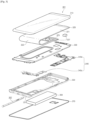
- FIG. 3 illustrates an exploded perspective view of an electronic device according to an embodiment.
- an electronic device 301 may include a cover glass 310, a display device 320, a front hardware module 327, a support member 330, a printed circuit board 340, a side member 350, a battery 360, and/or a back cover 370.
- the electronic device 301 may not include some of the components illustrated in FIG. 3 and may further include components not illustrated in FIG. 3 .
- the display device 320 may be disposed in a space between the cover glass 310 and the back cover 370.
- the display device 320 may be disposed on, or coupled to, the bottom of the cover glass 310 and may be exposed through at least a portion of the cover glass 310.
- the display device 320 may output contents (e.g., text, an image, a video, an icon, a widget, or a symbol), or may receive an input (e.g., a touch input or an electronic pen input) from the user.
- the touch panel may be inserted into the display panel (an add-on touch panel), may be directly formed on the display panel (an on-cell touch panel), or may be included in the display panel (an in-cell touch panel).
- the electronic pen sensor e.g., a digitizer
- the display panel including the touch panel may be referred to as a touch sensitive display panel.
- the display device 320 may include a screen area 321 and an extended area 322 that extends from one side (e.g., an upper side or a lower side) of the screen area 321.
- Pixels e.g., OLEDs
- electrical elements e.g., OLEDs
- a conductive pattern of the touch sensor e.g., OLEDs
- a conductive pattern of the electronic pen sensor may be arranged in the screen area 321.
- the electrical elements arranged in the screen area 321 may be electrically connected to a flexible printed circuit board (FPCB) 325 located on a rear surface of the display device 320 through various conductive patterns (interconnection wires).
- FPCB flexible printed circuit board
- the screen area 321 may include an active area.
- the active area which is a portion of the screen area 321, may include pixels arranged therein.
- the extended area 322 may include a bent area.
- the bent area may be understood as an area where one side of the display device 320 is bent toward the rear surface of the display device 320.
- the display device can include a flexible substrate, a thin film transistor (TFT) layer including a plurality of light-emitting elements, an insulation layer, and a touch sensor.
- TFT thin film transistor
- the extended area 322 may have a width that is substantially the same as (or within 5%), or different from, that of the screen area 321.
- the extended area 322 may be narrower than the screen area 321.
- the active area which is disposed in the screen area 321 and includes the pixels, may have a rectangular shape with rounded corners.
- various types of electronic parts, elements, and printed circuits e.g., a processor, a memory, a communication circuit (e.g., a wireless communication circuit), and the like) of the electronic device 301 may be mounted or arranged on the printed circuit boards 340m and 340s.
- the printed circuit boards 340m and 340s may be referred to as a main board, a printed board assembly (PBA), or simply a PCB.
- the side member 350 may be disposed between the printed circuit board 340 and the back cover 370 to accommodate components of the electronic device 301.
- the side member 350 may be combined with, for example, the support member 330 or the back cover 370 of the electronic device 301.
- the side member 350 may surround the space between the cover glass 310 and the back cover 370.
- a hole 351 extending long toward the inside of the side member 350 may be formed in a portion of the side member 350.
- an electronic pen (stylus pen) 302 may be accommodated in the hole 351.
- the battery 360 may convert chemical energy into electrical energy, and vice versa.
- the battery 360 may convert chemical energy into electrical energy and may supply the electrical energy to the display device 320 and various components or modules mounted on the printed circuit board 340.
- the battery 360 may also convert electrical energy supplied from the outside into chemical energy and may store the chemical energy.
- the printed circuit board 340 may include a power management module for managing charge/discharge of the battery 360.
- the back cover 370 may be coupled to a rear surface of the electronic device 301.
- the back cover 370 may be formed of reinforced glass, a plastic injection-molded material, and/or metal.
- the back cover 370 may be implemented integrally with the side member 350, or may be implemented to be detachable by a user.
- the back cover 370 may also be referred to as a rear case or a rear plate.
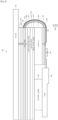
- the cover glass 410 may pass light generated by the display panel 440. According to an embodiment, a user may touch the cover glass 410 with a part (e.g., a finger) of the user's body to apply a touch input.
- a part e.g., a finger
- the OCA 420 which is a transparent adhesive layer, may stick the cover glass 410 and the polarizer 430 together. According to an embodiment, the OCA 420 may stick the polarizer 430 and the display panel 440 together.
- the display panel 440 may include, for example, scan lines, data lines, light-emitting elements (e.g., OLEDs) that generate light based on signals supplied from the scan lines and the data lines, a substrate (e.g., a low-temperature poly silicon (LTPS) substrate) on which the light-emitting elements are arranged, and a thin film encapsulation (TFE) for protecting the light-emitting elements.
- the light-emitting elements may configure pixels.
- a plurality of (e.g., millions to tens of millions of) pixels may be arranged on any one surface of the display panel 440 (e.g., a surface facing the cover glass 410).
- the display panel 440 may include a flexible substrate.
- the flexible substrate may extend from at least some layers of the display panel 440 to the outside.
- interconnection wire(s) for supplying power and/or signals to the display panel 440 may be arranged on the flexible substrate.
- the interconnection wires can include leads.
- a lead can connect a control circuit to the display panel, wherein a first lead connects the control circuit to light-emitting elements, and another lead can connect the control circuit to a touch sensor on the display panel.
- the display panel 440 may include a screen area 441 and extended areas 442 and 443.
- the extended areas 442 and 443 may include the bent area 442 and the planar area 443.
- a portion of the bent area 442 may be bent in a direction toward a rear surface of the display panel 440.
- a rear surface of the screen area 441 and a rear surface of the planar area 443 may face each other.
- the control circuit can be disposed under the planar area 443 with the leads traversing the extended areas connecting the control circuit to the light-emitting elements and touch sensor on the display panel.
- the display panel 440 may be divided into an active area and an inactive area.
- the active area may include light-emitting elements
- the inactive area may include the bent area 442.
- the protection film (PF) 460 may be stuck to the display panel 440 to protect the display panel 440.
- the BPL 450 which is a kind of insulator, may be stuck to the bent area 442 of the display panel 440.
- the BPL 450 may prevent the display panel 440 from being broken in the bent area 442 and may prevent cracks in leads arranged on the display panel 440.
- the neutral plane to which stress is applied in the bent area 442 may be located closer to the leads to lower the possibility of cracks in the leads than when the BPL 450 is not present.
- the back panel 470 may be disposed below the protection film 460.
- the back panel 470 may include at least one of a light-shielding layer 471 (e.g., a black layer including an uneven pattern) for shielding light generated by the display panel 440 or light incident from the outside, a buffer layer 472 (e.g., a sponge layer) for alleviating pressure from the outside, and a metal plate layer 473 (e.g., a copper (Cu) layer, or a graphite layer).
- a light-shielding layer 471 e.g., a black layer including an uneven pattern
- a buffer layer 472 e.g., a sponge layer
- a metal plate layer 473 e.g., a copper (Cu) layer, or a graphite layer
- the adhesive layer 480 may stick the metal plate layer 473 and the protection film 460 together.
- the adhesive layer 480 may physically support components above and below the adhesive layer 480.
- the display panel 501 in the screen area 5a may include light-emitting elements capable of emitting light according to electrical signals.
- the display panel 501 in the extended area 5b may include leads that electrically connect the light-emitting elements and/or the touch sensor 540 to the control circuit 502.
- the TFT layer 520 may be understood as a set of various types of electrical elements arranged on the flexible substrate 510.
- the TFT layer 520 may include a plurality of light-emitting elements.
- the plurality of light-emitting elements may correspond to, for example, organic light-emitting diodes (OLEDs).
- the touch sensor 540 may be disposed on the insulation layer 530.
- the touch sensor 540 may detect a user's touch on a cover glass of the electronic device 500 (e.g., the cover glass 410 of FIG. 4 ).
- the control circuit 502 is electrically connected to the display panel 501 and does control an operation of the display panel 501. Indeed, the control circuit 502 is electrically connected to the display panel 501 through the first leads 503 and the second leads 504.
- the control circuit 502 may include a display driver integrated circuit (DDI) and a touch sensor IC.
- the display driver IC and the touch sensor IC may be implemented with a single chip, or may be implemented with separate chips that are physically distinguished from each other.
- the extended area 5b of the display panel 501 may include in addition to the bent area (e.g., the bent area 442 of FIG. 4 ) a planar area (e.g., the planar area 443 of FIG. 4 ).
- the display driver IC may be disposed on the flexible substrate 510 corresponding to the planar area.
- the first leads 503 are formed on the TFT layer 520 in the screen area 5a and the extended area 5b. In other words, the first leads 503 may be formed below the insulation layer 530 in the screen area 5a and the extended area 5b.
- the first leads 503 do electrically connect the control circuit 502 and the plurality of light-emitting elements included in the TFT layer 520.
- the control circuit 502 may include the display driver IC.
- the first leads 503 do electrically connect the display driver IC and the plurality of light-emitting elements.
- the display driver IC may transmit power and/or image signals to the plurality of light-emitting elements through the first leads 503.
- the second leads 504 are formed on the insulation layer 530 in the screen area 5a and on the TFT layer 520 in the extended area 5b and extend from the screen area 5a to the extended area 5b through the one or more via-holes 511 formed in the insulation layer 530.
- the extended area 5b of the display panel 501 may include the bent area (e.g., the bent area 442 of FIG. 4 ) and additionally a planar area (e.g., the planar 443 area of FIG. 4 ).
- the second leads 504 extend from the bent area to the planar area through the one or more via-holes 512 formed in the insulation layer 530.
- the second leads 504 electrically connect the control circuit 502 and the touch sensor 540.
- the control circuit 502 may include the touch sensor IC.
- the second leads 504 may electrically connect the touch sensor IC and the touch sensor 540.
- the touch sensor IC may receive detected electrical signals from the touch sensor 540 through the second leads 504.
- first leads 503 may also be referred to as first interconnection wires
- second leads 504 may also be referred to as second interconnection wires.
- the display panel 501 may further include a second insulation layer (e.g., the BPL 450 of FIG. 4 ) that is distinguished from the insulation layer 530.
- the second insulation layer may be formed on the insulation layer 530.
- the second insulation layer may further reduce the risk of cracks in the first leads 503 and the second leads 504 in the bent area (e.g., the bent area 442 of FIG. 4 ) included in the extended area 5b.
- FIG. 6 illustrates an arrangement of leads in a display panel according to an embodiment.
- a blowup of a first area 620a of the flexible substrate 610a may be the same as, or similar to, a first area 620b.
- the first area 620b may be divided into a screen area 620_1b and an extended area 620_2b.
- First leads 621b and second leads 622b may be arranged on opposite layers in the screen area 620_1b.
- the first leads 621b may be arranged on an insulation layer (e.g., the insulation layer 530 of FIG. 5 ), and the second leads 622b may be arranged below the insulation layer (e.g., on the TFT layer 520 of FIG. 5 ) in the extended area 620_2b.
- the first leads 621b and the second leads 622b may vertically overlap each other.
- a sectional view taken along line A-A' in the extended area 620_2b of the first area 620b may be the same as, or similar to, a sectional view 620c.
- first leads 621c and second leads 622c may be arranged between an insulation layer 624c and a flexible substrate 625c (e.g., on a TFT layer). Since the first leads 621c and the second leads 622c are arranged on the same layer in the extended area 620_2b, the possibility of cracks due to an overlap between the leads may be lowered even though the display panel 601a is bent in the extended area 620_2b.
- the first leads 621c and the second leads 622c may be electrically isolated from each other. An electrical short may be prevented since the first leads 621c and the second leads 622c are electrically isolated from each other although arranged on the same layer.
- the display panel according to an embodiment of the present disclosure may have various lead patterns in the bent area.
- the bent area may correspond to, for example, the bent area 442 illustrated in FIG. 4 .
- a flexible substrate 701 illustrated in FIG. 7 may correspond to the flexible substrate 610a illustrated in FIG. 6 .
- leads 710 may be arranged in a zigzag pattern in a bent area 7-1 of the flexible substrate 701.
- leads 710 e.g., first leads and second leads
- leads 710 may be arranged in a zigzag pattern in a bent area 7-1 of the flexible substrate 701.
- the possibility of cracks in the leads may be lowered since tension exerted on the leads decreases even though the bent area 7-1 of the flexible substrate 701 is bent.
- leads e.g., first leads and second leads
- leads may be arranged in a wave pattern in the bent area 7-1 of the flexible substrate 701.
- the possibility of cracks in the leads may be lowered since tension exerted on the leads decreases even though the bent area 7-1 of the flexible substrate 701 is bent.
- leads e.g., first leads and second leads
- leads may be formed to have a specified width or more in the bent area 7-1 of the flexible substrate 701. Since the leads are formed to be relatively thick, resistance to tension generated when the bent area 7-1 of the flexible substrate 701 is bent may increase. As a result, the possibility of cracks in the leads may be lowered.
- leads e.g., first leads and second leads
- leads may be split into a specified number of leads in the bent area 7-1 of the flexible substrate 701.
- the leads may maintain an electrical connection even though some of the leads are cracked by tension generated when the bent area 7-1 of the flexible substrate 701 is bent.
- FIG. 8 illustrates an arrangement of leads in a display panel according to various embodiments.
- the first leads 822 and second leads 821 are on opposite sides of the flexible substrate 820b in both the screen area 820_1b and the edge area 820_2b.
- blowups of first areas 820a and 820_1a of the flexible substrates 810a and 810_1a may be the same as, or similar to, a first area 820b.
- the first area 820b may be divided into a screen area 820_1b and an extended area 820_2b.
- first leads 821b and second leads 822b may vertically overlap each other in the screen area 820_1b.
- the first leads 821b and the second leads 822b may be arranged in the extended area 820_2b so as not to vertically overlap each other.
- first leads 821c may be arranged between an insulation layer 823c and a flexible substrate 824c (e.g., on a TFT layer).
- Second leads 822c may be arranged on the top of the insulation layer 823c.
- first leads 821c and the second leads 822c do not vertically overlap each other even though arranged on different layers, the possibility of cracks due to an overlap between the leads may be lowered.
- the display panel 801a or 801_1a may further include a flexible substrate 825d distinguished from a flexible substrate 824d.
- first leads 821d may be arranged between an insulation layer 823d and the flexible substrate 824d.
- second leads 822d may be arranged between an insulation layer 823d and the flexible substrate 825d.
- the insulation layer 823d adjacent to the first leads 821d and the insulation layer 823d adjacent to the second leads 822d may be spaced apart from each other.
- since the first leads 821d and the second leads 822d do not vertically overlap each other even though arranged on different layers, the possibility of cracks due to an overlap between the leads may be lowered.
- FIG. 9 illustrates an arrangement of leads in a display panel according to an embodiment.
- a display panel 901a may include a flexible substrate 910a (e.g., the flexible substrate 510 of FIG. 5 ) that extends to the outside along some layers.
- first leads 911a and/or second leads 912a may be arranged on the flexible substrate 910a. The contents that overlap the description of FIG. 6 and the description of FIG. 8 may be omitted in the following description of FIG. 9 .
- a blowup of a first area 920a of the flexible substrate 910a may be the same as, or similar to, a first area 920b.
- a sectional view taken along line A-A' in the extended area 920_2b of the first area 920b may be the same as, or similar to, a sectional view 920c.
- first leads 921c may be arranged between an insulation layer 923c and a flexible substrate 924c (e.g., on a TFT layer).
- Second leads 922c may be arranged on the top of the insulation layer 923c.
- first leads 921c and the second leads 922c are alternately arranged so as not to vertically overlap each other even though arranged on different layers, the possibility of cracks due to an overlap between the leads may be lowered.
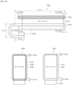
- FIG. 10 illustrates a structure of an electronic device according to an embodiment.
- the electronic devices 1000a, 1000b, and 1000c may correspond to, for example, the electronic device 101 illustrated in FIG. 1 .
- the polarizer 1020a may be longer than the active area. In an embodiment, the polarizer 1020a may completely surround the display panel 1010a corresponding to the active area and may protect the display panel 1010a from an external impact.
- the polarizer 1020a may be longer than a lower portion of the active area by a first length d1 1021a and may be longer than an upper portion of the active area by a second length d2 1022a.
- the first length d1 1021a may be longer than the second length d2 1022a since the extension of an upper portion of the electronic device 1000a is limited in consideration of minimization of a bezel.
- the polarizer 1020a may protect the active area of the display panel 1010a from an external impact.
- the first polymer film 1030a may correspond to, for example, the flexible substrate 510 of FIG. 5 .
- the first polymer film 1030a may constitute a part of the display panel 1010a, and various types of electrical elements included in the display panel 1010a may be arranged on the first polymer film 1030a.
- the first polymer film 1030a may be implemented with polyethylene terephthalate (PET), polyethylene naphthalate (PEN), polyethylene sulfide (PES), polyethylene (PE), or polyimide (PI).
- the second polymer film 1040a may be longer than the active area. In an embodiment, the second polymer film 1040a may completely surround the display panel 1010a corresponding to the active area and may protect the display panel 1010a from an external impact applied from below the display panel 1010a.
- the second polymer film 1040a may be longer than the lower portion of the active area by a third length d3 1043a and may be longer than the upper portion of the active area by a fourth length d4 1044a.
- the third length d3 1043a may be longer than the fourth length d4 1044a since the extension of the upper portion of the electronic device 1000a is limited in consideration of minimization of the bezel.
- the second polymer film 1040a may protect the active area of the display panel 1010a from an external impact applied from below the display panel 1010a.
- the polarizer 1020a and the second polymer film 1040a may be limited to the screen area 10-1a or the planar area 10-3a of the display panel 1010a.
- the polarizer 1020a and the second polymer film 1040a may not be disposed in the bent area 10-2a of the display panel 1010a.
- the display panel 1010a may be more flexibly bent in the bent area 10-2a and may prevent cracks in leads arranged in the bent area 10-2a.
- the relative sizes of an active area of a display panel 1010b, a polarizer 1020b, and a first polymer film 1030b may be compared.
- the polarizer 1020b may be implemented to be larger than the active area of the display panel 1010b and smaller than the first polymer film 1030b.
- the polarizer 1020b may be longer than an upper portion of the active area by a length d2 1022b and may be longer than a lower portion of the active area by a length d1 1021b. In this case, the length d1 1021b may be longer than the length d2 1022b.
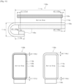
- FIG. 11 illustrates a structure of an electronic device according to an embodiment.
- the polarizer 1120a and the second polymer film 1140a may be wider than an active area of the display panel 1110a to protect the display panel 1110a from an external impact.
- the electronic device 1100a may protect the active area of the display panel 1110a and may allow a bent area 11-2a of the display panel 1110a to be more easily bent.
- the second polymer film 1140a may be further away from the bent area 11-2a of the display panel 1110a to allow the bent area 11-2a of the display panel 1110a to be more easily bent.
- a length d3 1143a may be shorter than a length d4 1144a.
- the second polymer film 1140a may allow the bent area 11-2a of the display panel 1110a to be more easily bent.
- the relative sizes of an active area of a display panel 1110c, a first polymer film 1130c, and a second polymer film 1140c may be compared.
- the second polymer film 1140c may be longer than an upper portion of the active area by a length d4 1144c and may be longer than a lower portion of the active area by a length d3 1143c.
- the length d3 1143c may be shorter than the length d4 1144c.
- module used herein may represent, for example, a unit including one or more combinations of hardware, software and firmware.
- module may be interchangeably used with the terms “logic”, “logical block”, “part” and “circuit”.
- the “module” may be a minimum unit of an integrated part or may be a part thereof.
- the “module” may be a minimum unit for performing one or more functions or a part thereof.
- the “module” may include an application-specific integrated circuit (ASIC).
- ASIC application-specific integrated circuit
- the machine-readable storage media may be provided in the form of non-transitory storage media.
- non-transitory is a limitation of the medium itself (i.e., tangible, not a signal) as opposed to a limitation on data storage persistency.
- the method according to various embodiments disclosed in the present disclosure may be provided as a part of a computer program product.
- the computer program product may be traded between a seller and a buyer as a product.
- the computer program product may be distributed in the form of machine-readable storage medium (e.g., a compact disc read only memory (CD-ROM)) or may be distributed only through an application store (e.g., a Play Store ).
- an application store e.g., a Play Store
- at least a portion of the computer program product may be temporarily stored or generated in a storage medium such as a memory of a manufacturer's server, an application store's server, or a relay server.
Landscapes
- Engineering & Computer Science (AREA)
- Theoretical Computer Science (AREA)
- Physics & Mathematics (AREA)
- General Engineering & Computer Science (AREA)
- General Physics & Mathematics (AREA)
- Human Computer Interaction (AREA)
- Computer Hardware Design (AREA)
- Nonlinear Science (AREA)
- Optics & Photonics (AREA)
- Computer Networks & Wireless Communication (AREA)
- Microelectronics & Electronic Packaging (AREA)
- Mathematical Physics (AREA)
- Chemical & Material Sciences (AREA)
- Crystallography & Structural Chemistry (AREA)
- Devices For Indicating Variable Information By Combining Individual Elements (AREA)
- Electroluminescent Light Sources (AREA)
Description
- Embodiments of the present disclosure described herein relate to an electronic device including a display panel.
- Various types of electronic devices, such as a smartphone, a tablet personal computer (PC), and the like, which include a display. The displays of the electronic devices may be implemented with what is called a touch screen display that includes a touch panel. The electronic devices may execute various functions, such as taking a photo or video, reproducing a music or video file, playing a game, doing a search on the Internet, and the like, through the touch screen display.
- In recent years, many attempts have been made to minimize a bezel area of an electronic device at the same time as making a touch screen display larger in size.
- The above information is presented as background information only to assist with an understanding of the present disclosure. No determination has been made, and no assertion is made, as to whether any of the above might be applicable as prior art with regard to the present disclosure.
US20170090661 A1 relates to a touch screen panel and display device comprising the same.US 2017/207276 relates to a display device.US20160093685A1 relates to a flexible display device with bend stress reduction member and manufacturing method for the same.US20180267649A1 relates to an organic light emitting touch display screen.US20150060817A1 relates to a display device.US20180356921A1 relates to a touch display screen. - A flexible display panel may be used to make a display of an electronic device larger in size and to minimize a bezel area. In this case, a lower substrate of the display may be bent, and various types of hardware modules may be arranged below a front surface of the electronic device. As a result, a display area may maximized on the front surface of the electronic device, while the bezel area may be minimized.
- The hardware modules below the front surface of the electronic device may be connected to electrical elements in a screen area of the display through leads arranged in a bent area of the display panel. For example, a display driver IC may be connected to light-emitting elements through the leads arranged in the bent area of the display panel. In another example, a touch sensor IC may be connected to a touch sensor through the leads arranged in the bent area of the display panel.
- In the case where various types of leads are arranged in the bent area, tension or stress exerted on the leads may increase with an increase in curvature of the bent area. When the lower substrate of the display is bent, the path across the display between two points elongates causing tension to be exerted on the leads. Especially, in the case where the leads vertically overlap one another, stronger tension may be exerted on leads disposed on the outside of the bent area under the influence of leads disposed on the inside of the bent area.
- The increased tension exerted on the leads may increase the possibility of cracks in the leads, or reduce the time period before wear and tear result in cracks, causing a malfunction in the display of the electronic device.
- Aspects of the present disclosure may address at least the above-mentioned problems and/or disadvantages and may provide at least some of the advantages described below. Accordingly, an aspect of the present disclosure is to provide a method that may lower the possibility of cracks in leads arranged in a display panel and an electronic device for performing the same.
- The present invention is defined in claim 1. Furthere aspects of the invention are defined in the dependent claims.
- According to embodiments of the present disclosure, it is possible to lower the possibility of cracks in leads arranged in a bent area of a display panel in an electronic device. Accordingly, it is possible to set the curvature of the bent area to a larger value and to minimize a bezel area with an increase in size of a screen area where the display panel is exposed. In addition, the present disclosure may provide various effects that are directly or indirectly recognized.
- Other aspects, advantages, and salient features of the disclosure will become apparent to those skilled in the art from the following detailed description, which, taken in conjunction with the annexed drawings, discloses various embodiments of the present disclosure.
- The above and other aspects, features, and advantages of certain embodiments of the present disclosure will be more apparent from the following description taken in conjunction with the accompanying drawings, in which:
-
FIG. 1 is a block diagram of an electronic device, which includes a flexible display panel, in a network environment according to various embodiments; -
FIG. 2 is a block diagram of a display device, which includes a flexible display panel, according to various embodiments; -
FIG. 3 illustrates an exploded perspective view of an electronic device according to an embodiment; -
FIG. 4 illustrates an arrangement structure of a hardware module of an electronic device according to an embodiment; -
FIG. 5 illustrates a configuration of an electronic device according to an embodiment; -
FIG. 6 illustrates an arrangement of leads in a display panel according to an embodiment; -
FIG. 7 illustrates an arrangement of leads in a bent area of a display panel according to an embodiment; -
FIG. 8 illustrates an arrangement of leads in a display panel according to various embodiments; -
FIG. 9 illustrates an arrangement of leads in a display panel according to an embodiment; -
FIG. 10 illustrates a structure of an electronic device according to an embodiment; and -
FIG. 11 illustrates a structure of an electronic device according to an embodiment. - Throughout the drawings, it should be noted that like reference numerals are used to depict the same or similar components, features, and structures.
-
FIG. 1 is a block diagram of anelectronic device 101, which includes a flexible display panel, in anetwork environment 100 according to various embodiments. The flexible display panel may be bent to maximize the display area on the front surface and reduce the bezel area. - Referring to
FIG. 1 , theelectronic device 101 may communicate with anelectronic device 102 through a first network 198 (e.g., a short-range wireless communication) or may communicate with anelectronic device 104 or aserver 108 through a second network 199 (e.g., a long-distance wireless communication) in thenetwork environment 100. According to an embodiment, theelectronic device 101 may communicate with theelectronic device 104 through theserver 108. According to an embodiment, theelectronic device 101 may include aprocessor 120, amemory 130, aninput device 150, asound output device 155, adisplay device 160, anaudio module 170, asensor module 176, aninterface 177, ahaptic module 179, acamera module 180, apower management module 188, abattery 189, acommunication module 190, asubscriber identification module 196, and anantenna module 197. According to some embodiments, at least one of the components of theelectronic device 101 may be omitted or other components may be added to theelectronic device 101. According to some embodiments, some components may be integrated and implemented as in the case of the sensor module 176 (e.g., a fingerprint sensor, an iris sensor, or an illuminance sensor) embedded in the display device 160 (e.g., a display). - The
processor 120 may operate, for example, software (e.g., a program 140) to control at least one of other components (e.g., a hardware or software component) of theelectronic device 101 connected to theprocessor 120 and may process and compute a variety of data. Theprocessor 120 may load a command set or data, which is received from other components (e.g., thesensor module 176 or the communication module 190), into avolatile memory 132, may process the loaded command or data, and may store result data into anonvolatile memory 134. According to an embodiment, theprocessor 120 may include a main processor 121 (e.g., a central processing unit or an application processor) and an coprocessor 123(e.g., a graphic processing device, an image signal processor, a sensor hub processor, or a communication processor), which operates independently from themain processor 121, additionally or alternatively uses less power than themain processor 121, or is specified to a designated function. In this case, the coprocessor123 may operate separately from themain processor 121 or embedded. - In this case, the
coprocessor 123 may control, for example, at least some of functions or states associated with at least one component (e.g., thedisplay device 160, thesensor module 176, or the communication module 190) among the components of the electronic device 101instead of themain processor 121 while themain processor 121 is in an inactive (e.g., sleep) state or together with themain processor 121 while themain processor 121 is in an active (e.g., an application execution) state. According to an embodiment, the coprocessor123 (e.g., the image signal processor or the communication processor) may be implemented as a part of another component (e.g., thecamera module 180 or the communication module 190) that is functionally related to the coprocessor123. Thememory 130 may store a variety of data used by at least one component (e.g., theprocessor 120 or the sensor module 176) of theelectronic device 101, for example, software (e.g., the program 140) and input data or output data with respect to commands associated with the software. The memory 130may include thevolatile memory 132 or thenonvolatile memory 134. - The
program 140 may be stored in thememory 130 as software and may include, for example, anoperating system 142, amiddleware 144, or anapplication 146. - The
input device 150 may be a device for receiving a command or data, which is used for a component (e.g., the processor 120) of theelectronic device 101, from an outside (e.g., a user) of theelectronic device 101 and may include, for example, a microphone, a mouse, or a keyboard. - The
sound output device 155 may be a device for outputting a sound signal to the outside of theelectronic device 101 and may include, for example, a speaker used for general purposes, such as multimedia play or recordings play, and a receiver used only for receiving calls. According to an embodiment, the receiver and the speaker may be either integrally or separately implemented. - The
display device 160 may be a device for visually presenting information to the user and may include, for example, a display, and a control circuit for controlling a corresponding device. According to an embodiment, thedisplay device 160 may include a touch circuitry or a pressure sensor for measuring an intensity of pressure on the touch. Thedisplay device 160 will be described in greater detail inFigure 2 . In certain embodiments, the display may include a lower substrate that is bent, thereby increasing the display area. Hardware modules below the display may be connected to components in the screen area using leads. Although the substrate is bent, in certain embodiments, increased tension exerted on the leads is alleviated as will be described below. - The
audio module 170 may convert a sound and an electrical signal in dual directions. According to an embodiment, theaudio module 170 may obtain the sound through theinput device 150 or may output the sound through an external electronic device (e.g., the electronic device 102 (e.g., a speaker or a headphone)) wired or wirelessly connected to thesound output device 155 or theelectronic device 101. - The
sensor module 176 may generate an electrical signal or a data value corresponding to an operating state (e.g., power or temperature) inside or an environmental state outside theelectronic device 101. The sensor module 176may include, for example, a gesture sensor, a gyro sensor, a barometric pressure sensor, a magnetic sensor, an acceleration sensor, a grip sensor, a proximity sensor, a color sensor, an infrared sensor, a biometric sensor, a temperature sensor, a humidity sensor, or an illuminance sensor. - The
interface 177 may support a designated protocol wired or wirelessly connected to the external electronic device (e.g., the electronic device 102). According to an embodiment, theinterface 177 may include, for example, an HDMI (high-definition multimedia interface), a USB (universal serial bus) interface, an SD card interface, or an audio interface. - A
connection terminal 178 may include a connector that physically connects theelectronic device 101 to the external electronic device (e.g., the electronic device 102), for example, an HDMI connector, a USB connector, an SD card connector, or an audio connector (e.g., a headphone connector). - The
haptic module 179 may convert an electrical signal to a mechanical stimulation (e.g., vibration or movement) or an electrical stimulation perceived by the user through tactile or kinesthetic sensations. Thehaptic module 179 may include, for example, a motor, a piezoelectric element, or an electric stimulator. - The
camera module 180 may shoot a still image or a video image. According to an embodiment, thecamera module 180 may include, for example, at least one lens, an image sensor, an image signal processor, or a flash. - The
power management module 188 may be a module for managing power supplied to theelectronic device 101 and may serve as at least a part of a power management integrated circuit (PMIC). - The
battery 189 may be a device for supplying power to at least one component of theelectronic device 101 and may include, for example, a non-rechargeable (primary) battery, a rechargeable (secondary) battery, or a fuel cell. - The
communication module 190 may establish a wired or wireless communication channel between theelectronic device 101 and the external electronic device (e.g., theelectronic device 102, theelectronic device 104, or the server 108) and support communication execution through the established communication channel. Thecommunication module 190 may include at least one communication processor operating independently from the processor 120 (e.g., the application processor) and supporting the wired communication or the wireless communication. According to an embodiment, the communication module 190may include a wireless communication module 192 (e.g., a cellular communication module, a short-range wireless communication module, or a GNSS (global navigation satellite system) communication module) or a wired communication module 194 (e.g., an LAN (local area network) communication module or a power line communication module) and may communicate with the external electronic device using a corresponding communication module among them through the first network 198 (e.g., the short-range communication network such as a Bluetooth, a WiFi direct, or an IrDA (infrared data association)) or the second network 199 (e.g., the long-distance wireless communication network such as a cellular network, an internet, or a computer network (e.g., LAN or WAN)). The above-mentionedvarious communication modules 190 may be implemented into one chip or into separate chips, respectively. - According to an embodiment, the wireless communication module 192may identify and authenticate the
electronic device 101 using user information stored in thesubscriber identification module 196 in the communication network. - The
antenna module 197 may include one or more antennas to transmit or receive the signal or power to or from an external source. According to an embodiment, the communication module 190 (e.g., the wireless communication module 192) may transmit or receive the signal to or from the external electronic device through the antenna suitable for the communication method. - Some components among the components may be connected to each other through a communication method (e.g., a bus, a GPIO (general purpose input/output), an SPI (serial peripheral interface), or an MIPI (mobile industry processor interface)) used between peripheral devices to exchange signals (e.g., a command or data) with each other.
- According to an embodiment, the command or data may be transmitted or received between the
electronic device 101 and the externalelectronic device 104 through theserver 108 connected to thesecond network 199. Each of theelectronic devices electronic device 101. According to an embodiment, all or some of the operations performed by theelectronic device 101 may be performed by another electronic device or a plurality of external electronic devices. When theelectronic device 101 performs some functions or services automatically or by request, theelectronic device 101 may request the external electronic device to perform at least some of the functions related to the functions or services, in addition to or instead of performing the functions or services by itself. The external electronic device receiving the request may carry out the requested function or the additional function and transmit the result to theelectronic device 101. Theelectronic device 101 may provide the requested functions or services based on the received result as is or after additionally processing the received result. To this end, for example, a cloud computing, distributed computing, or client-server computing technology may be used. -
FIG. 2 is a block diagram 200 of thedisplay device 160, which includes a flexible display panel, according to various embodiments. - Referring to
FIG. 2 , thedisplay device 160 may include adisplay 210 and a display driver IC (DDI) 230 for controlling thedisplay 210. TheDDI 230 may include aninterface module 231, a memory 233 (e.g., a buffer memory), animage processing module 235, or amapping module 237. TheDDI 230 may receive image information including image data or an image control signal corresponding to a command for controlling the image data, from the processor 120 (e.g., the main processor 121 (e.g., an application processor) or thecoprocessor 123 operating independently of the main processor 121) through theinterface module 231. - The
DDI 230 may be in communication withtouch circuitry 250 or thesensor module 176 through theinterface module 231. Furthermore, theDDI 230 may store at least a portion of the received image information in thememory 233, for example, on a frame-by-frame basis. Theimage processing module 235 may pre-process or post-process at least a part of the image data (e.g., adjust the resolution, brightness, or size thereof), based at least on characteristics of the image data or characteristics of thedisplay 210. Themapping module 237 may convert the image data pre-processed or post-processed through theimage processing module 235 into a voltage or current value for driving pixels of thedisplay 210, based at least partly on properties of the pixels (e.g., an arrangement of the pixels (RGB stripe or PenTile) or the sizes of subpixels). At least some pixels of thedisplay 210 may be driven based on the voltage or current value, and visual information (e.g., text, an image, or an icon) corresponding to the image data may be displayed on thedisplay 210 correspondingly. In certain embodiments, theDDI 160 can be disposed on a flexible substrate corresponding to a planar area. - According to an embodiment, the
display device 160 may further include thetouch circuitry 250. Thetouch circuitry 250 may include atouch sensor 251 and atouch sensor IC 253 for controlling thetouch sensor 251. Thetouch sensor IC 253 may control thetouch sensor 251 to measure a change in signal (e.g., voltage, an amount of light, resistance, or an amount of electric charge) for a specific location of thedisplay 210 to detect a touch or hovering input to the specific location and may provide, to theprocessor 120, information (e.g., location, area, pressure, or time) about the detected touch or hovering input. According to an embodiment, at least a part (e.g., the touch sensor IC 253) of thetouch circuitry 250 may be included as a part of thedisplay driver IC 230 or thedisplay 210 or a part of another component (e.g., the coprocessor 123) disposed outside thedisplay device 160. In certain embodiments, thetouch sensor IC 253 and thetouch sensor 251 can be connected by a lead. - According to an embodiment, the
display device 160 may further include at least one sensor (e.g., a fingerprint sensor, an iris sensor, a pressure sensor, or an illuminance sensor) of thesensor module 176 or a control circuit for the at least one sensor. In this case, the at least one sensor or the control circuit for the same may be embedded and implemented in a part (e.g., thedisplay 210 or the DDI 230) of thedisplay device 160 or a part of thetouch circuitry 250. For example, in the case where thesensor module 176 embedded in thedisplay device 160 includes a biometric sensor (e.g., a fingerprint sensor), the biometric sensor may obtain biometric information (e.g., a fingerprint image) associated with a touch input, through a partial area of thedisplay 210. In another example, in the case where thesensor module 176 embedded in thedisplay device 160 includes a pressure sensor, the pressure sensor may obtain pressure information on a touch input, through all or a part of thedisplay 210. According to an embodiment, thetouch sensor 251 or thesensor module 176 may be disposed between pixels in a pixel layer of thedisplay 210 or above or below the pixel layer. -
FIG. 3 illustrates an exploded perspective view of an electronic device according to an embodiment. - Referring to
FIG. 3 , anelectronic device 301 according to an embodiment (e.g., theelectronic device 101 ofFIG. 1 ) may include acover glass 310, adisplay device 320, afront hardware module 327, asupport member 330, a printedcircuit board 340, aside member 350, abattery 360, and/or aback cover 370. According to various embodiments, theelectronic device 301 may not include some of the components illustrated inFIG. 3 and may further include components not illustrated inFIG. 3 . - According to an embodiment, the
cover glass 310 may pass light generated by thedisplay device 320. In another example, a user may touch thecover glass 310 with a part (e.g., a finger) of the user's body to provide a touch input (including contact using an electronic pen) to theelectronic device 301. Thecover glass 310 may be formed of, for example, reinforced glass, reinforced plastic, a flexible polymer, or the like and may protect thedisplay device 320 and components included in theelectronic device 301 from an external impact. According to various embodiments, thecover glass 310 may also be referred to as a glass window or a transparent member. - According to an embodiment, the
display device 320 may be disposed in a space between thecover glass 310 and theback cover 370. For example, thedisplay device 320 may be disposed on, or coupled to, the bottom of thecover glass 310 and may be exposed through at least a portion of thecover glass 310. Thedisplay device 320 may output contents (e.g., text, an image, a video, an icon, a widget, or a symbol), or may receive an input (e.g., a touch input or an electronic pen input) from the user. - According to an embodiment, the
display device 320 may include a display panel, a touch sensor, and/or an electronic pen sensor. The display panel may include, for example, a liquid crystal display (LCD) panel, a light-emitting diode (LED) display panel, an organic light-emitting diode (OLED) display panel, a microelectrome-chanical systems (MEMS) display panel, or an electronic paper display panel. The touch sensor may include a capacitive touch panel, a pressure-sensitive touch panel, a resistive touch panel, an infrared touch panel, or an ultrasonic touch panel. The touch panel may be inserted into the display panel (an add-on touch panel), may be directly formed on the display panel (an on-cell touch panel), or may be included in the display panel (an in-cell touch panel). The electronic pen sensor (e.g., a digitizer) may detect a touch, a gesture, hovering, or the like from an electronic pen. In various embodiments, the display panel including the touch panel may be referred to as a touch sensitive display panel. - According to an embodiment, the
display device 320 may include ascreen area 321 and anextended area 322 that extends from one side (e.g., an upper side or a lower side) of thescreen area 321. Pixels (e.g., OLEDs) of the display panel, electrical elements, a conductive pattern of the touch sensor, and/or a conductive pattern of the electronic pen sensor may be arranged in thescreen area 321. The electrical elements arranged in thescreen area 321 may be electrically connected to a flexible printed circuit board (FPCB) 325 located on a rear surface of thedisplay device 320 through various conductive patterns (interconnection wires). - According to an embodiment, the
screen area 321 may include an active area. The active area, which is a portion of thescreen area 321, may include pixels arranged therein. - According to an embodiment, the
extended area 322 may include a bent area. The bent area may be understood as an area where one side of thedisplay device 320 is bent toward the rear surface of thedisplay device 320. - In certain embodiments, the display device can include a flexible substrate, a thin film transistor (TFT) layer including a plurality of light-emitting elements, an insulation layer, and a touch sensor.
- According to various embodiments, interconnection wiring of the
FPCB 325 may pass by a side surface of thesupport member 330 and may be electrically connected to the printed circuit board 340 (e.g., a main printedcircuit board 340m) through a specified connector. According to various embodiments, theextended area 322 may include pixels arranged therein for displaying various pieces of information, similarly to thescreen area 321. - According to an embodiment, the
extended area 322 may have a width that is substantially the same as (or within 5%), or different from, that of thescreen area 321. For example, theextended area 322 may be narrower than thescreen area 321. In this case, the active area, which is disposed in thescreen area 321 and includes the pixels, may have a rectangular shape with rounded corners. - According to an embodiment, the
front hardware module 327 may include various components, such as a fingerprint sensor, a camera module, a proximity sensor, an iris sensor, a receiver, and the like, which are arranged to face a front surface of theelectronic device 301. Thefront hardware module 327 may be disposed below thedisplay device 320. For example, thefront hardware module 327 may be disposed between a specified area of thedisplay device 320 and theback cover 370 and may be arranged to face thecover glass 310. - According to an embodiment, the support member 330 (e.g., a bracket) may be formed of metal or a polymer. The
support member 330 may be disposed, for example, between thedisplay device 320 and the printedcircuit board 340. Thesupport member 330 may be combined with thedisplay device 320 and the printedcircuit board 340 to physically support thedisplay device 320 and the printedcircuit board 340. According to an embodiment, thesupport member 330 may have a swelling gap formed therein in consideration of swelling of thebattery 360 according to a secular change. - According to an embodiment, the printed
circuit board 340 may include, for example, the main printedcircuit board 340m and asub-printed circuit board 340s. According to an embodiment, the main printedcircuit board 340m and thesub-printed circuit board 340s may be disposed below thesupport member 330 and may be electrically connected together through a specified connector or specified interconnection wiring. The printedcircuit boards electronic device 301 may be mounted or arranged on the printedcircuit boards circuit boards - According to an embodiment, the
side member 350 may be disposed between the printedcircuit board 340 and theback cover 370 to accommodate components of theelectronic device 301. Theside member 350 may be combined with, for example, thesupport member 330 or theback cover 370 of theelectronic device 301. Theside member 350 may surround the space between thecover glass 310 and theback cover 370. According to various embodiments, ahole 351 extending long toward the inside of theside member 350 may be formed in a portion of theside member 350. For example, an electronic pen (stylus pen) 302 may be accommodated in thehole 351. - According to an embodiment, the
battery 360 may convert chemical energy into electrical energy, and vice versa. For example, thebattery 360 may convert chemical energy into electrical energy and may supply the electrical energy to thedisplay device 320 and various components or modules mounted on the printedcircuit board 340. In another example, thebattery 360 may also convert electrical energy supplied from the outside into chemical energy and may store the chemical energy. According to an embodiment, the printedcircuit board 340 may include a power management module for managing charge/discharge of thebattery 360. - According to an embodiment, the
back cover 370 may be coupled to a rear surface of theelectronic device 301. Theback cover 370 may be formed of reinforced glass, a plastic injection-molded material, and/or metal. According to various embodiments, theback cover 370 may be implemented integrally with theside member 350, or may be implemented to be detachable by a user. Theback cover 370 may also be referred to as a rear case or a rear plate. -
FIG. 4 illustrates a hardware configuration of an electronic device according to an embodiment. - Referring to
FIG. 4 , anelectronic device 400 may include acover glass 410, an optical clear adhesive (OCA) 420, a polarizer (POL) 430, adisplay panel 440, a bending protecting layer (BPL) 450, a protection film (PF) 460, aback panel 470, anadhesive layer 480, apressure sensor 490, a display driver IC (DDI) 401, and/or a flexible printed circuit board (FPCB) 402. According to various embodiments, the electronic device 400 (e.g., theelectronic device 101 ofFIG. 1 ) may not include some of the components illustrated inFIG. 4 and may further include components not illustrated inFIG. 4 . For example, among the components illustrated inFIG. 4 , adjacent components may be attached to each other by an adhesive tape not illustrated inFIG. 4 . - The
cover glass 410 may pass light generated by thedisplay panel 440. According to an embodiment, a user may touch thecover glass 410 with a part (e.g., a finger) of the user's body to apply a touch input. - The
OCA 420, which is a transparent adhesive layer, may stick thecover glass 410 and thepolarizer 430 together. According to an embodiment, theOCA 420 may stick thepolarizer 430 and thedisplay panel 440 together. - The
polarizer 430 may prevent reflection of external light to improve visibility in bright places such as the outdoors. For example, the polarizer (or polarizer film) 430 may improve visibility by passing only light waves oscillating in a specific direction among light waves input through thecover glass 410. In various embodiments, thepolarizer 430 may include, for example, poly ethylene terephthalate (PET) or tri-acetyl cellulose (TAC). - The
display panel 440 may include, for example, scan lines, data lines, light-emitting elements (e.g., OLEDs) that generate light based on signals supplied from the scan lines and the data lines, a substrate (e.g., a low-temperature poly silicon (LTPS) substrate) on which the light-emitting elements are arranged, and a thin film encapsulation (TFE) for protecting the light-emitting elements. The light-emitting elements may configure pixels. A plurality of (e.g., millions to tens of millions of) pixels may be arranged on any one surface of the display panel 440 (e.g., a surface facing the cover glass 410). - According to an embodiment, the
display panel 440 may include a flexible substrate. According to an embodiment, the flexible substrate may extend from at least some layers of thedisplay panel 440 to the outside. According to an embodiment, interconnection wire(s) for supplying power and/or signals to thedisplay panel 440 may be arranged on the flexible substrate. For example, the interconnection wires can include leads. A lead can connect a control circuit to the display panel, wherein a first lead connects the control circuit to light-emitting elements, and another lead can connect the control circuit to a touch sensor on the display panel. - According to an embodiment, the
display panel 440 may include ascreen area 441 andextended areas extended areas bent area 442 and theplanar area 443. In an embodiment, a portion of thebent area 442 may be bent in a direction toward a rear surface of thedisplay panel 440. In this case, a rear surface of thescreen area 441 and a rear surface of theplanar area 443 may face each other. In certain embodiments, the control circuit can be disposed under theplanar area 443 with the leads traversing the extended areas connecting the control circuit to the light-emitting elements and touch sensor on the display panel. - According to an embodiment, the
display panel 440 may be divided into an active area and an inactive area. In an embodiment, the active area may include light-emitting elements, and the inactive area may include thebent area 442. - According to an embodiment, the protection film (PF) 460 may be stuck to the
display panel 440 to protect thedisplay panel 440. - According to an embodiment, the
BPL 450, which is a kind of insulator, may be stuck to thebent area 442 of thedisplay panel 440. TheBPL 450 may prevent thedisplay panel 440 from being broken in thebent area 442 and may prevent cracks in leads arranged on thedisplay panel 440. For example, when theBPL 450 is disposed on thebent area 442, the neutral plane to which stress is applied in thebent area 442 may be located closer to the leads to lower the possibility of cracks in the leads than when theBPL 450 is not present. - According to an embodiment, the
back panel 470 may be disposed below theprotection film 460. Theback panel 470 may include at least one of a light-shielding layer 471 (e.g., a black layer including an uneven pattern) for shielding light generated by thedisplay panel 440 or light incident from the outside, a buffer layer 472 (e.g., a sponge layer) for alleviating pressure from the outside, and a metal plate layer 473 (e.g., a copper (Cu) layer, or a graphite layer). - According to an embodiment, an opening (e.g., an opening with a thickness of 0.1 mm to 0.18 mm) may be formed in at least a partial area of the
back panel 470. A fingerprint sensor (not illustrated) may be disposed in an area corresponding to the opening. According to an embodiment, the fingerprint sensor may obtain fingerprint information of a finger through the opening. In the case where the fingerprint sensor is of an optical type, the fingerprint sensor may be disposed in the area corresponding to the opening. In the case where the fingerprint sensor is of a capacitive type, the opening may not be formed in theback panel 470, or the fingerprint sensor may be disposed regardless of the opening. - According to an embodiment, the
adhesive layer 480 may stick themetal plate layer 473 and theprotection film 460 together. Theadhesive layer 480 may physically support components above and below theadhesive layer 480. - According to an embodiment, the
pressure sensor 490 may be disposed to correspond to the entire surface of thedisplay panel 440, or may be disposed in only a partial area of thedisplay panel 440. Thepressure sensor 490 may be disposed to surround the fingerprint sensor. According to an embodiment, thepressure sensor 490 may obtain the magnitude of pressure of a user input (e.g., an input using a finger or an electronic pen) that is applied to thecover glass 410. - According to an embodiment, the
DDI 401 may drive the pixels of thedisplay panel 440. For example, theDDI 401 may receive image data from a processor (a host) and may supply signals corresponding to the image data to thedisplay panel 440 based on a preset number of frames. According to an embodiment, theDDI 401 may be disposed on a surface of theplanar area 443 of thedisplay panel 440. In certain embodiments, theDDI 401 may be connected by a lead to a light-emitting elements on thescreen area 441. - According to an embodiment, the
FPCB 402 may be electrically connected to a portion of thedisplay panel 440. For example, theFPCB 402 may be electrically connected to the interconnection wires formed on the substrate of thedisplay panel 440. According to an embodiment, theFPCB 402 may include leads for supplying scan signals to a touch sensor included in thedisplay panel 440. - According to an embodiment, the
FPCB 402 may include interconnection wiring related to the components illustrated inFIG. 4 . TheFPCB 402 may correspond to, for example, theFPCB 325 illustrated inFIG. 3 . For example, the interconnection wiring of theFPCB 402 may pass by a side surface of thesupport member 330 illustrated inFIG. 3 and may be electrically connected to the printed circuit board 340 (e.g., the main printedcircuit board 340m) through a specified connector. - The curvature of the
display panel 440 increases the display area, but can cause tension in wires traversing theextended areas 442. As will be described in certain embodiments below, the tension caused by the curvature ofextended area 442 can be alleviated. -
FIG. 5 illustrates a configuration of an electronic device according to an embodiment. - Referring to
FIG. 5 , an electronic device 500 (e.g., theelectronic device 400 ofFIG. 4 ) may include a touch sensitive display panel 501 (e.g., thedisplay panel 440 ofFIG. 4 ), acontrol circuit 502, first leads 503, and second leads 504. According to various embodiments, theelectronic device 500 may not include some of the components, or may include additional components. The touchsensitive display panel 501 may include aflexible substrate 510, a thin film transistor (TFT)layer 520, aninsulation layer 530, and atouch sensor 540. According to an embodiment, the touchsensitive display panel 501 may be divided into ascreen area 5a and anextended area 5b. In an embodiment, theextended area 5b may be bent toward a rear surface of thedisplay panel 501. - According to an embodiment, the
display panel 501 in thescreen area 5a may include light-emitting elements capable of emitting light according to electrical signals. Thedisplay panel 501 in theextended area 5b may include leads that electrically connect the light-emitting elements and/or thetouch sensor 540 to thecontrol circuit 502. - According to an embodiment, the
flexible substrate 510 may be a substrate made of plastic or a polymer. In various embodiments, theflexible substrate 510 may include at least one of, for example, polyethylene terephthalate (PET), polyethylene naphthalate (PEN), polyethylene sulfide (PES), polyethylene (PE), and polyimide (PI). In various embodiments, theflexible substrate 510 may also be referred to as a flexible printed circuit board. - According to an embodiment, leads and electrical elements for supplying power and/ or signals to the
display panel 501 may be arranged on theflexible substrate 510. For example, leads, transistors, and light-emitting elements included in theTFT layer 520 may be arranged on theflexible substrate 510. - According to an embodiment, the
TFT layer 520 may be understood as a set of various types of electrical elements arranged on theflexible substrate 510. For example, theTFT layer 520 may include a plurality of light-emitting elements. The plurality of light-emitting elements may correspond to, for example, organic light-emitting diodes (OLEDs). - In various embodiments, the arrangement of the electrical elements on the
TFT layer 520 may be understood to be the same as, or similar to, the formation of the electrical elements on theflexible substrate 510. - According to an embodiment, the
insulation layer 530 may be formed on theTFT layer 520. According to an embodiment, theinsulation layer 530 may be applied onto theTFT layer 520 to prevent electrical short between the electrical elements included in theTFT layer 520. In an embodiment, a portion of theinsulation layer 530 may be a thin film encapsulation. The thin film encapsulation may protect the plurality of light-emitting elements from moisture or oxygen by forming, for example, a plurality of organic layers and/or inorganic layers. - According to an embodiment, the
insulation layer 530 may have via-holes holes holes screen area 5a and theextended area 5b. In various embodiments, the via-holes screen area 5a or theextended area 5b. In an embodiment, leads (e.g., the second leads 504) may extend from the top to the bottom of theinsulation layer 530 through the via-holes - According to an embodiment, the
touch sensor 540 may be disposed on theinsulation layer 530. Thetouch sensor 540 may detect a user's touch on a cover glass of the electronic device 500 (e.g., thecover glass 410 ofFIG. 4 ). - According to an embodiment, the
touch sensor 540 may include a touch electrode. The touch electrode may be a terminal for a signal transmitted to or from thetouch sensor 540. The touch electrode may be disposed, for example, on or over theflexible substrate 510. For example, the touch electrode may be directly formed on theflexible substrate 510, or may be disposed on or over theinsulation layer 530 or a conductive layer (not illustrated) disposed over theflexible substrate 510. - The
control circuit 502 is electrically connected to thedisplay panel 501 and does control an operation of thedisplay panel 501. Indeed, thecontrol circuit 502 is electrically connected to thedisplay panel 501 through the first leads 503 and the second leads 504. - According to an embodiment, the
control circuit 502 may include a display driver integrated circuit (DDI) and a touch sensor IC. In various embodiments, the display driver IC and the touch sensor IC may be implemented with a single chip, or may be implemented with separate chips that are physically distinguished from each other. According to an embodiment, theextended area 5b of thedisplay panel 501 may include in addition to the bent area (e.g., thebent area 442 ofFIG. 4 ) a planar area (e.g., theplanar area 443 ofFIG. 4 ). In this case, the display driver IC may be disposed on theflexible substrate 510 corresponding to the planar area. - The first leads 503 are formed on the
TFT layer 520 in thescreen area 5a and theextended area 5b. In other words, the first leads 503 may be formed below theinsulation layer 530 in thescreen area 5a and theextended area 5b. - According to an embodiment, the first leads 503 do electrically connect the
control circuit 502 and the plurality of light-emitting elements included in theTFT layer 520. According to an embodiment, thecontrol circuit 502 may include the display driver IC. The first leads 503 do electrically connect the display driver IC and the plurality of light-emitting elements. In an embodiment, the display driver IC may transmit power and/or image signals to the plurality of light-emitting elements through the first leads 503. - The second leads 504 are formed on the
insulation layer 530 in thescreen area 5a and on theTFT layer 520 in theextended area 5b and extend from thescreen area 5a to theextended area 5b through the one or more via-holes 511 formed in theinsulation layer 530. According to an embodiment, theextended area 5b of thedisplay panel 501 may include the bent area (e.g., thebent area 442 ofFIG. 4 ) and additionally a planar area (e.g., the planar 443 area ofFIG. 4 ). In this case, the second leads 504 extend from the bent area to the planar area through the one or more via-holes 512 formed in theinsulation layer 530. - The second leads 504 electrically connect the
control circuit 502 and thetouch sensor 540. According to an embodiment, thecontrol circuit 502 may include the touch sensor IC. The second leads 504 may electrically connect the touch sensor IC and thetouch sensor 540. In an embodiment, the touch sensor IC may receive detected electrical signals from thetouch sensor 540 through the second leads 504. - According to various embodiments, the first leads 503 may also be referred to as first interconnection wires, and the second leads 504 may also be referred to as second interconnection wires.
- The first leads 503 and the second leads 504 may be formed on the same layer in the
extended area 5b according to the above-described lead arrangement and may not vertically overlap each other. That is, the first leads 503 and the second leads 504 may not overlap each other when viewed in a direction perpendicular to the bent area (e.g., thebent area 442 ofFIG. 4 ). The lead arrangement may lower the possibility of cracks in the first leads 503 and/or the second leads 504. - According to an embodiment, the
display panel 501 may further include a second insulation layer (e.g., theBPL 450 ofFIG. 4 ) that is distinguished from theinsulation layer 530. In an embodiment, the second insulation layer may be formed on theinsulation layer 530. The second insulation layer may further reduce the risk of cracks in the first leads 503 and the second leads 504 in the bent area (e.g., thebent area 442 ofFIG. 4 ) included in theextended area 5b. -
FIG. 6 illustrates an arrangement of leads in a display panel according to an embodiment. - Referring to
FIG. 6 , adisplay panel 601a may include aflexible substrate 610a (e.g., theflexible substrate 510 ofFIG. 5 ) that extends to the outside along some layers. In an embodiment, theflexible substrate 610a may have first leads (e.g., the first leads 503 ofFIG. 5 ) and/or second leads (e.g., the second leads 504 ofFIG. 5 ) arranged thereon. According to an embodiment, a portion of the flexible substrate may be a screen area (e.g., thescreen area 5a ofFIG. 5 ), and the remaining portion may be an extendedarea 610a (e.g., theextended area 5b ofFIG. 5 ). - According to an embodiment, a blowup of a
first area 620a of theflexible substrate 610a may be the same as, or similar to, afirst area 620b. Thefirst area 620b may be divided into a screen area 620_1b and an extended area 620_2b. First leads 621b andsecond leads 622b may be arranged on opposite layers in the screen area 620_1b. For example, the first leads 621b may be arranged on an insulation layer (e.g., theinsulation layer 530 ofFIG. 5 ), and the second leads 622b may be arranged below the insulation layer (e.g., on theTFT layer 520 ofFIG. 5 ) in the extended area 620_2b. In this case, the first leads 621b and the second leads 622b may vertically overlap each other. - According to an embodiment, one or more via-
holes 623b may be formed in the insulation layer in the vicinity of the border between the screen area 620_1b and the extended area 620_2b. In an embodiment, the second leads 622b may extend from the screen area 620_1b to the extended area 620_2b through the via-holes 623b. In other words, the second leads 622b may extend from the top to the bottom of the insulation layer through the via-holes 623b. - According to an embodiment, a sectional view taken along line A-A' in the extended area 620_2b of the
first area 620b may be the same as, or similar to, asectional view 620c. In an embodiment, referring to thesectional view 620c, first leads 621c andsecond leads 622c may be arranged between aninsulation layer 624c and aflexible substrate 625c (e.g., on a TFT layer). Since the first leads 621c and the second leads 622c are arranged on the same layer in the extended area 620_2b, the possibility of cracks due to an overlap between the leads may be lowered even though thedisplay panel 601a is bent in the extended area 620_2b. - According to an embodiment, the first leads 621c and the second leads 622c may be electrically isolated from each other. An electrical short may be prevented since the first leads 621c and the second leads 622c are electrically isolated from each other although arranged on the same layer.
-
FIG. 7 illustrates an arrangement of leads in a bent area of a display panel according to an embodiment. - Referring to
FIG. 7 , the display panel according to an embodiment of the present disclosure may have various lead patterns in the bent area. The bent area may correspond to, for example, thebent area 442 illustrated inFIG. 4 . Aflexible substrate 701 illustrated inFIG. 7 may correspond to theflexible substrate 610a illustrated inFIG. 6 . - When the bent area 7-1 of the
flexible substrate 701 is bent, the distance between two points on theflexible substrate 701 increases. This can cause tension in leads. In various embodiments, the leads have a longer length, due to zig-zagging, or wave patterning, and increased thickness, to prevent cracks due to the tension. - According to an embodiment, leads 710 (e.g., first leads and second leads) may be arranged in a zigzag pattern in a bent area 7-1 of the
flexible substrate 701. In this case, the possibility of cracks in the leads may be lowered since tension exerted on the leads decreases even though the bent area 7-1 of theflexible substrate 701 is bent. - According to another embodiment, unlike that illustrated in
FIG. 7 , leads (e.g., first leads and second leads) may be arranged in the bent area 7-1 of theflexible substrate 701 such that the leads extend at a specified angle (e.g., obliquely) with respect to the vertical direction. In this case, the possibility of cracks in the leads may be lowered since tension exerted on the leads decreases even though the bent area 7-1 of theflexible substrate 701 is bent. - According to another embodiment, unlike that illustrated in
FIG. 7 , leads (e.g., first leads and second leads) may be arranged in a wave pattern in the bent area 7-1 of theflexible substrate 701. In this case, the possibility of cracks in the leads may be lowered since tension exerted on the leads decreases even though the bent area 7-1 of theflexible substrate 701 is bent. - According to another embodiment, unlike that illustrated in
FIG. 7 , leads (e.g., first leads and second leads) may be formed to have a specified width or more in the bent area 7-1 of theflexible substrate 701. Since the leads are formed to be relatively thick, resistance to tension generated when the bent area 7-1 of theflexible substrate 701 is bent may increase. As a result, the possibility of cracks in the leads may be lowered. - According to another embodiment, unlike that illustrated in
FIG. 7 , leads (e.g., first leads and second leads) may be split into a specified number of leads in the bent area 7-1 of theflexible substrate 701. The leads may maintain an electrical connection even though some of the leads are cracked by tension generated when the bent area 7-1 of theflexible substrate 701 is bent. -
FIG. 8 illustrates an arrangement of leads in a display panel according to various embodiments. InFigure 8 , the first leads 822 and second leads 821 are on opposite sides of theflexible substrate 820b in both the screen area 820_1b and the edge area 820_2b. - Referring to
FIG. 8 , adisplay panel 801a or 801_1a may include aflexible substrate 810a or 810_1a (e.g., theflexible substrate 510 ofFIG. 5 ) that extends to the outside along some layers. In an embodiment, first leads 811a and/orsecond leads 812a may be arranged on theflexible substrate 810a, and first leads 811_1a and/or second leads 812_1a may be arranged on the flexible substrate 810_1a. According to various embodiments, the first leads 811a and thesecond leads 812a may be arranged such that the same type of leads are adjacent to one another, and the second leads 812_1a may be arranged on opposite sides of the first leads 811_1a. The contents that overlap the description ofFIG. 6 may be omitted in the following description ofFIG. 8 . - According to an embodiment, blowups of
first areas 820a and 820_1a of theflexible substrates 810a and 810_1a may be the same as, or similar to, afirst area 820b. - The
first area 820b may be divided into a screen area 820_1b and an extended area 820_2b. According to an embodiment, first leads 821b andsecond leads 822b may vertically overlap each other in the screen area 820_1b. According to an embodiment, the first leads 821b and the second leads 822b may be arranged in the extended area 820_2b so as not to vertically overlap each other. - According to an embodiment, a sectional view taken along line A-A' in the extended area 820_2b of the
first area 820b may be the same as, or similar to, asectional view - In an embodiment, referring to the
sectional view 820c, first leads 821c may be arranged between aninsulation layer 823c and aflexible substrate 824c (e.g., on a TFT layer). Second leads 822c may be arranged on the top of theinsulation layer 823c. In an embodiment, since the first leads 821c and the second leads 822c do not vertically overlap each other even though arranged on different layers, the possibility of cracks due to an overlap between the leads may be lowered. - In an embodiment, referring to the
sectional view 820d, thedisplay panel 801a or 801_1a may further include aflexible substrate 825d distinguished from aflexible substrate 824d. In an embodiment, first leads 821d may be arranged between aninsulation layer 823d and theflexible substrate 824d. In an embodiment, second leads 822d may be arranged between aninsulation layer 823d and theflexible substrate 825d. In this case, theinsulation layer 823d adjacent to the first leads 821d and theinsulation layer 823d adjacent to the second leads 822d may be spaced apart from each other. In an embodiment, since the first leads 821d and thesecond leads 822d do not vertically overlap each other even though arranged on different layers, the possibility of cracks due to an overlap between the leads may be lowered. -
FIG. 9 illustrates an arrangement of leads in a display panel according to an embodiment. - Referring to
FIG. 9 , adisplay panel 901a may include aflexible substrate 910a (e.g., theflexible substrate 510 ofFIG. 5 ) that extends to the outside along some layers. In an embodiment, first leads 911a and/orsecond leads 912a may be arranged on theflexible substrate 910a. The contents that overlap the description ofFIG. 6 and the description ofFIG. 8 may be omitted in the following description ofFIG. 9 . - According to an embodiment, a blowup of a
first area 920a of theflexible substrate 910a may be the same as, or similar to, afirst area 920b. - The
first area 920b may be divided into a screen area 920_1b and an extended area 920_2b. According to an embodiment, first leads 921b andsecond leads 922b may vertically overlap each other in the screen area 920_1b. According to an embodiment, the first leads 921b and the second leads 922b may be alternately arranged in the extended area 920_2b so as not to vertically overlap each other. - According to an embodiment, a sectional view taken along line A-A' in the extended area 920_2b of the
first area 920b may be the same as, or similar to, asectional view 920c. - In an embodiment, referring to the
sectional view 920c, first leads 921c may be arranged between aninsulation layer 923c and aflexible substrate 924c (e.g., on a TFT layer). Second leads 922c may be arranged on the top of theinsulation layer 923c. In an embodiment, since the first leads 921c and the second leads 922c are alternately arranged so as not to vertically overlap each other even though arranged on different layers, the possibility of cracks due to an overlap between the leads may be lowered. -
FIG. 10 illustrates a structure of an electronic device according to an embodiment. - Referring to
FIG. 10 , stack structures and front views ofelectronic devices electronic devices electronic device 101 illustrated inFIG. 1 . - In an embodiment, the
electronic device 1000a may include adisplay panel 1010a, apolarizer 1020a, afirst polymer film 1030a, and asecond polymer film 1040a. In various embodiments, theelectronic device 1000a may not include some of the components or may include additional components, or one component may be included in another component. For example, thefirst polymer film 1030a may be understood as a component of thedisplay panel 1010a. - The
display panel 1010a may correspond to, for example, thedisplay panel 440 ofFIG. 4 or thedisplay panel 501 ofFIG. 5 . According to an embodiment, thedisplay panel 1010a may be divided into a plurality of areas. For example, thedisplay panel 1010a may be divided into a screen area 10-1a and extended areas 10-2a and 10-3a. The extended areas 10-2a and 10-3a may be divided into the bent area 10-2a and the planar area 10-3a. It may be understood that only an active area of thedisplay panel 1010a is illustrated inFIG. 10 . The active area may be, for example, a portion of the screen area 10-1a of thedisplay panel 1010a and may be understood as an area where pixels are arranged. A plurality of light-emitting elements may be densely arranged in the active area of thedisplay panel 1010a. - The
polarizer 1020a may correspond to, for example, thepolarizer 430 ofFIG. 4 . In various embodiments, thepolarizer 1020a may include, for example, a poly ethylene terephthalate (PET) film, a tri-acetyl cellulose (TAC) film, a cycle-olefin polymer (COP) film, or a poly-vinyl alcohol (PVA) film. - According to an embodiment, the
polarizer 1020a may be longer than the active area. In an embodiment, thepolarizer 1020a may completely surround thedisplay panel 1010a corresponding to the active area and may protect thedisplay panel 1010a from an external impact. - According to an embodiment, the
polarizer 1020a may be longer than a lower portion of the active area by afirst length d1 1021a and may be longer than an upper portion of the active area by asecond length d2 1022a. In an embodiment, thefirst length d1 1021a may be longer than thesecond length d2 1022a since the extension of an upper portion of theelectronic device 1000a is limited in consideration of minimization of a bezel. By making thefirst length d1 1021a longer than thesecond length d2 1022a, thepolarizer 1020a may protect the active area of thedisplay panel 1010a from an external impact. - The
first polymer film 1030a may correspond to, for example, theflexible substrate 510 ofFIG. 5 . Thefirst polymer film 1030a may constitute a part of thedisplay panel 1010a, and various types of electrical elements included in thedisplay panel 1010a may be arranged on thefirst polymer film 1030a. In various embodiments, thefirst polymer film 1030a may be implemented with polyethylene terephthalate (PET), polyethylene naphthalate (PEN), polyethylene sulfide (PES), polyethylene (PE), or polyimide (PI). - The
second polymer film 1040a may correspond to, for example, theprotection film 460 ofFIG. 4 . According to an embodiment, thesecond polymer film 1040a may be attached to a lower portion of thedisplay panel 1010a to protect thedisplay panel 1010a from an external impact applied from below thedisplay panel 1010a. According to various embodiments, thesecond polymer film 1040a may be implemented with a material that is the same as, or similar to, that of thefirst polymer film 1030a. - According to an embodiment, the
second polymer film 1040a may be longer than the active area. In an embodiment, thesecond polymer film 1040a may completely surround thedisplay panel 1010a corresponding to the active area and may protect thedisplay panel 1010a from an external impact applied from below thedisplay panel 1010a. - According to an embodiment, the
second polymer film 1040a may be longer than the lower portion of the active area by athird length d3 1043a and may be longer than the upper portion of the active area by afourth length d4 1044a. In an embodiment, thethird length d3 1043a may be longer than thefourth length d4 1044a since the extension of the upper portion of theelectronic device 1000a is limited in consideration of minimization of the bezel. By making thethird length d3 1043a longer than thefourth length d4 1044a, thesecond polymer film 1040a may protect the active area of thedisplay panel 1010a from an external impact applied from below thedisplay panel 1010a. - According to an embodiment, the
polarizer 1020a and thesecond polymer film 1040a may be limited to the screen area 10-1a or the planar area 10-3a of thedisplay panel 1010a. In other words, thepolarizer 1020a and thesecond polymer film 1040a may not be disposed in the bent area 10-2a of thedisplay panel 1010a. As a result, thedisplay panel 1010a may be more flexibly bent in the bent area 10-2a and may prevent cracks in leads arranged in the bent area 10-2a. - Referring to the front view of the
electronic device 1000b, the relative sizes of an active area of adisplay panel 1010b, apolarizer 1020b, and afirst polymer film 1030b may be compared. According to an embodiment, thepolarizer 1020b may be implemented to be larger than the active area of thedisplay panel 1010b and smaller than thefirst polymer film 1030b. In an embodiment, thepolarizer 1020b may be longer than an upper portion of the active area by alength d2 1022b and may be longer than a lower portion of the active area by alength d1 1021b. In this case, thelength d1 1021b may be longer than thelength d2 1022b. - Referring to the front view of the
electronic device 1000c, the relative sizes of an active area of adisplay panel 1010c, afirst polymer film 1030c, and asecond polymer film 1040c may be compared. According to an embodiment, thesecond polymer film 1040c may be implemented to be larger than the active area of thedisplay panel 1010c. According to an embodiment, thesecond polymer film 1040c may be implemented to be smaller than thefirst polymer film 1030c so as to be attached to thefirst polymer film 1030c. In an embodiment, thesecond polymer film 1040c may be longer than an upper portion of the active area by alength d4 1044c and may be longer than a lower portion of the active area by alength d3 1043c. In this case, thelength d3 1043c may be longer than thelength d4 1044c. -
FIG. 11 illustrates a structure of an electronic device according to an embodiment. - Referring to
FIG. 11 , stack structures and front views ofelectronic devices electronic devices electronic devices FIG. 10 . The contents that overlap the description ofFIG. 10 may be omitted in the following description ofFIG. 11 . - In an embodiment, the
electronic device 1100a may include adisplay panel 1110a, apolarizer 1120a, afirst polymer film 1130a, and asecond polymer film 1140a. - According to an embodiment, the
polarizer 1120a and thesecond polymer film 1140a may be wider than an active area of thedisplay panel 1110a to protect thedisplay panel 1110a from an external impact. - According to an embodiment, the
electronic device 1100a may protect the active area of thedisplay panel 1110a and may allow a bent area 11-2a of thedisplay panel 1110a to be more easily bent. According to an embodiment, thesecond polymer film 1140a may be further away from the bent area 11-2a of thedisplay panel 1110a to allow the bent area 11-2a of thedisplay panel 1110a to be more easily bent. In this case, alength d3 1143a may be shorter than alength d4 1144a. In an embodiment, by making thelength d3 1143a shorter than thelength d4 1144a, thesecond polymer film 1140a may allow the bent area 11-2a of thedisplay panel 1110a to be more easily bent. - Referring to the front view of the
electronic device 1100c, the relative sizes of an active area of adisplay panel 1110c, afirst polymer film 1130c, and asecond polymer film 1140c may be compared. According to an embodiment, thesecond polymer film 1140c may be longer than an upper portion of the active area by alength d4 1144c and may be longer than a lower portion of the active area by alength d3 1143c. In this case, thelength d3 1143c may be shorter than thelength d4 1144c. - According to embodiments of the present disclosure, by arranging leads in a bent area of a display of an electronic device that includes a display panel, it is possible to reduce the risk of cracks in the leads.
- With the reduction in the risk of cracks in the leads, the curvature of the display panel in the electronic device may be set to be larger. Accordingly, a bezel area may be minimized with an increase in size of a screen area through which the display is exposed in the electronic device. The electronic device may provide better visibility for a user.
- The electronic device according to various embodiments disclosed in the present disclosure may be various types of devices. The electronic device may include, for example, at least one of a portable communication device (e.g., a smartphone), a computer device, a portable multimedia device, a mobile medical appliance, a camera, a wearable device, or a home appliance. The electronic device according to an embodiment of the present disclosure should not be limited to the above-mentioned devices.
- The term "module" used herein may represent, for example, a unit including one or more combinations of hardware, software and firmware. The term "module" may be interchangeably used with the terms "logic", "logical block", "part" and "circuit". The "module" may be a minimum unit of an integrated part or may be a part thereof. The "module" may be a minimum unit for performing one or more functions or a part thereof. For example, the "module" may include an application-specific integrated circuit (ASIC).
- Various embodiments of the present disclosure may be implemented by software (e.g., the program 140) including an instruction stored in a machine-readable storage media (e.g., an
internal memory 136 or an external memory 138) readable by a machine (e.g., a computer). The machine may be a device that calls the instruction from the machine-readable storage media and operates depending on the called instruction and may include the electronic device (e.g., the electronic device 101). When the instruction is executed by the processor (e.g., the processor 120), the processor may perform a function corresponding to the instruction directly or using other components under the control of the processor. The instruction may include a code generated or executed by a compiler or an interpreter. The machine-readable storage media may be provided in the form of non-transitory storage media. Here, the term "non-transitory", as used herein, is a limitation of the medium itself (i.e., tangible, not a signal) as opposed to a limitation on data storage persistency. - According to an embodiment, the method according to various embodiments disclosed in the present disclosure may be provided as a part of a computer program product. The computer program product may be traded between a seller and a buyer as a product. The computer program product may be distributed in the form of machine-readable storage medium (e.g., a compact disc read only memory (CD-ROM)) or may be distributed only through an application store (e.g., a Play Store). In the case of online distribution, at least a portion of the computer program product may be temporarily stored or generated in a storage medium such as a memory of a manufacturer's server, an application store's server, or a relay server.

Claims (13)
- An electronic device (301) comprising:a first lead (503)(621c)(821c)(821d)(921c);a second lead (504)(822b)(622c)(822d)(922c);a touch sensitive display panel (501)(601a)(801a)(901a) including a screen area (5a) and an extended area (5b) that extends from the screen area (5a); anda control circuit (502) electrically connected to the touch sensitive display panel (501) (601a)(801a)(901a) through the first lead (503) and the second lead (504),wherein the touch sensitive display panel (501)(601a)(801a)(901a) includes:a flexible substrate (510);a thin film transistor (TFT) layer (520) formed on the flexible substrate (510) and including a plurality of light-emitting elements;an insulation layer (530) that is disposed on the TFT layer (520) and in which a via-hole (511) is formed; anda touch sensor (540) disposed on the insulation layer (530),wherein the first lead (503)(621c)(821c)(821d)(921c) is formed on the TFT layer (520) in the screen area (5a) and the extended area (5b) and connects the control circuit (502) and the plurality of light-emitting elements,the second lead (504)(822b)(622c)(822d)(922c) is formed on the insulation layer (530) in the screen area (5a) and on the TFT layer (520) in the extended area (5b) and extends from the screen area to the extended area (5b) through the via-hole (511) formed in the insulation layer (530), the second lead (504) connecting the control circuit (502) and the touch sensor (540),wherein the extended area (5b) includes a bent area (442)(620_2b)(820_2b)(920_2b), andcharacterized in that the first lead (503)(621c)(821c)(821d)(921c) and the second lead (504)(822b)(622c)(822d)(922c) do not overlap each other in the bent area (442)(620_2b)(820_2b)(920_2b) when viewed in a direction perpendicular to the bent area (442)(620_2b)(820_2b)(920_2b) of the touch sensitive display panel (501)(601a)(801a)(901a).
- The electronic device (301) of claim 1,
wherein at least a section of the bent area is bent toward a rear surface of the touch sensitive display panel (501). - The electronic device (301) of claim 1, wherein the first lead (503) and the second lead (504) are electrically isolated from each other.
- The electronic device (301) of claim 1, wherein the flexible substrate (510) includes polyimide (PI).
- The electronic device (301) of claim 1, wherein the control circuit (502) includes a display driver IC (230) and a touch sensor IC (253),wherein the first lead (503) connects the display driver IC (230) and the plurality of light-emitting elements, andwherein the second lead (504) connects the touch sensor IC (253) and the touch sensor (251).
- The electronic device (301) of claim 5, wherein the extended area (5b) further includes a planar area (443), the bent area being provided between the display area and the planar area, and
wherein the display driver IC (230) is disposed on the flexible substrate (510) corresponding to the planar area. - The electronic device (301) of claim 1, wherein the plurality of light-emitting elements include organic light-emitting diodes (OLEDs).
- The electronic device (301) of claim 1, wherein a portion of the insulation layer (530) in the screen area (5a) includes a thin film encapsulation (TFE).
- The electronic device (301) of claim 1, wherein the first lead (503) and the second lead (504) are arranged in a zigzag pattern in the bent area.
- The electronic device (301) of claim 1,
wherein the first lead (503) and the second lead (504) are split into a specified number of leads in the bent area. - The electronic device (301) of claim 1,
wherein the first lead (503) and the second lead (504) are obliquely arranged in the bent area. - The electronic device (301) of claim 1, wherein the first lead (503) and the second lead (504) are arranged in a wave pattern in the bent area.
- The electronic device (301) of claim 1, wherein the touch sensitive display panel (501) further includes a second insulation layer distinguished from the insulation layer (530),
wherein the second insulation layer is formed on the insulation layer (530) in the bent area.
Applications Claiming Priority (2)
| Application Number | Priority Date | Filing Date | Title |
|---|---|---|---|
| KR1020170098289A KR102517092B1 (en) | 2017-08-02 | 2017-08-02 | An electronic device comprising a flexible display panel |
| PCT/KR2018/008777 WO2019027266A1 (en) | 2017-08-02 | 2018-08-02 | Electronic device including flexible display panel |
Publications (3)
| Publication Number | Publication Date |
|---|---|
| EP3642822A1 EP3642822A1 (en) | 2020-04-29 |
| EP3642822A4 EP3642822A4 (en) | 2020-06-24 |
| EP3642822B1 true EP3642822B1 (en) | 2025-04-09 |
Family
ID=65230662
Family Applications (1)
| Application Number | Title | Priority Date | Filing Date |
|---|---|---|---|
| EP18841908.9A Active EP3642822B1 (en) | 2017-08-02 | 2018-08-02 | Electronic device including flexible display panel |
Country Status (5)
| Country | Link |
|---|---|
| US (1) | US11201195B2 (en) |
| EP (1) | EP3642822B1 (en) |
| KR (1) | KR102517092B1 (en) |
| CN (1) | CN109388278B (en) |
| WO (1) | WO2019027266A1 (en) |
Families Citing this family (19)
| Publication number | Priority date | Publication date | Assignee | Title |
|---|---|---|---|---|
| US10732747B2 (en) * | 2018-05-24 | 2020-08-04 | Innolux Corporation | Display device |
| CA3016051A1 (en) * | 2018-08-31 | 2020-02-29 | Alain Carel | A method of providing power input to a flexible printed circuit and a flexible printed circuit having power input in accordance with the method. |
| KR102644091B1 (en) * | 2018-12-20 | 2024-03-06 | 삼성디스플레이 주식회사 | Display device |
| CN113454788A (en) * | 2019-03-19 | 2021-09-28 | 希迪普公司 | Display device |
| KR102793085B1 (en) * | 2019-03-22 | 2025-04-08 | 삼성디스플레이 주식회사 | Touch sensing device and display device comprising the same |
| CN110196655B (en) * | 2019-05-14 | 2023-11-28 | 武汉华星光电半导体显示技术有限公司 | Pressure sensing touch screen and input device comprising same |
| KR102804702B1 (en) * | 2019-06-28 | 2025-05-12 | 엘지디스플레이 주식회사 | Display device |
| KR20210035382A (en) * | 2019-09-23 | 2021-04-01 | 삼성디스플레이 주식회사 | Display device and carrier panel |
| KR102823806B1 (en) * | 2019-12-31 | 2025-06-20 | 엘지디스플레이 주식회사 | Display apparatus |
| CN111105717B (en) * | 2020-01-14 | 2022-01-25 | 合肥维信诺科技有限公司 | Display panel and display device |
| KR20210091867A (en) * | 2020-01-14 | 2021-07-23 | 삼성디스플레이 주식회사 | Display device |
| CN111258453B (en) | 2020-01-15 | 2026-04-21 | 京东方科技集团股份有限公司 | A touch panel, its manufacturing method and display device |
| EP4095655B1 (en) * | 2020-01-22 | 2026-03-18 | Hideep Inc. | Electronic device, stylus pen, and method for driving and controlling same |
| CN111416892A (en) * | 2020-02-18 | 2020-07-14 | Oppo广东移动通信有限公司 | Electronic device |
| CN111399689A (en) * | 2020-04-23 | 2020-07-10 | 深圳莱宝高科技股份有限公司 | Flexible circuit board, display screen and touch screen |
| KR102937329B1 (en) * | 2020-07-10 | 2026-03-11 | 삼성디스플레이 주식회사 | Digitizer and display apparatus having the same |
| KR20220060078A (en) * | 2020-11-03 | 2022-05-11 | 삼성디스플레이 주식회사 | Display device |
| CN114171561B (en) * | 2021-11-12 | 2026-03-06 | 云谷(固安)科技有限公司 | Display panel and display device |
| CN114446174B (en) | 2022-02-11 | 2024-03-15 | 武汉华星光电半导体显示技术有限公司 | Display panels and mobile terminals |
Citations (2)
| Publication number | Priority date | Publication date | Assignee | Title |
|---|---|---|---|---|
| US20150325631A1 (en) * | 2014-05-09 | 2015-11-12 | Semiconductor Energy Laboratory Co., Ltd. | Display device, light-emitting device, and electronic appliance |
| US20200225545A1 (en) * | 2017-02-08 | 2020-07-16 | Boe Technology Group Co., Ltd. | Display substrate, display panel, display device and bonding method |
Family Cites Families (33)
| Publication number | Priority date | Publication date | Assignee | Title |
|---|---|---|---|---|
| GB0515175D0 (en) * | 2005-07-25 | 2005-08-31 | Plastic Logic Ltd | Flexible resistive touch screen |
| US20110134075A1 (en) * | 2008-08-07 | 2011-06-09 | Sharp Kabushiki Kaisha | Touch panel, display, and electronic device |
| KR101408715B1 (en) * | 2008-09-19 | 2014-06-17 | 가부시키가이샤 한도오따이 에네루기 켄큐쇼 | Display device |
| KR101803720B1 (en) * | 2008-10-03 | 2017-12-01 | 가부시키가이샤 한도오따이 에네루기 켄큐쇼 | Display device |
| WO2011043195A1 (en) * | 2009-10-09 | 2011-04-14 | Semiconductor Energy Laboratory Co., Ltd. | Semiconductor device |
| KR101320384B1 (en) * | 2011-06-30 | 2013-10-23 | 삼성디스플레이 주식회사 | Flexible display panel and the display apparatus comprising the flexible display panel |
| US9419065B2 (en) * | 2012-08-07 | 2016-08-16 | Apple Inc. | Flexible displays |
| US9195108B2 (en) | 2012-08-21 | 2015-11-24 | Apple Inc. | Displays with bent signal lines |
| KR102097150B1 (en) * | 2013-02-01 | 2020-04-03 | 엘지디스플레이 주식회사 | Flexible display substrate, flexible organic light emitting display device and method for manufacturing the same |
| KR101796812B1 (en) * | 2013-02-15 | 2017-11-10 | 엘지디스플레이 주식회사 | Flexible organic light emitting display device and method of manufacturing the same |
| US9740035B2 (en) * | 2013-02-15 | 2017-08-22 | Lg Display Co., Ltd. | Flexible organic light emitting display device and method for manufacturing the same |
| JP6253923B2 (en) | 2013-08-30 | 2017-12-27 | 株式会社ジャパンディスプレイ | Organic electroluminescence device with built-in touch sensor |
| TWI520324B (en) * | 2013-11-05 | 2016-02-01 | 群創光電股份有限公司 | Display panel with conductive pattern change area |
| KR102145961B1 (en) * | 2013-12-18 | 2020-08-20 | 삼성디스플레이 주식회사 | Organic light emitting device |
| KR102086644B1 (en) * | 2013-12-31 | 2020-03-09 | 엘지디스플레이 주식회사 | Flexible display device and manufacturing method thereof |
| US9544994B2 (en) * | 2014-08-30 | 2017-01-10 | Lg Display Co., Ltd. | Flexible display device with side crack protection structure and manufacturing method for the same |
| US9425418B2 (en) | 2014-09-30 | 2016-08-23 | Lg Display Co., Ltd. | Flexible display device with bend stress reduction member and manufacturing method for the same |
| US9600112B2 (en) * | 2014-10-10 | 2017-03-21 | Apple Inc. | Signal trace patterns for flexible substrates |
| US9614168B2 (en) * | 2015-01-12 | 2017-04-04 | Apple Inc. | Flexible display panel with bent substrate |
| KR102416467B1 (en) * | 2015-07-30 | 2022-07-04 | 엘지디스플레이 주식회사 | Touch screen panel and display device |
| US9778772B2 (en) * | 2015-09-16 | 2017-10-03 | Microsoft Technology Licensing, Llc | Bendable device with display in movable connection with body |
| KR102394723B1 (en) * | 2015-09-30 | 2022-05-09 | 엘지디스플레이 주식회사 | Touch screen panel and display device comprising the same |
| CN105718105B (en) * | 2015-12-25 | 2018-12-11 | 业成科技(成都)有限公司 | Organic Light Emitting Diode touch-control display panel |
| KR102439350B1 (en) * | 2015-12-31 | 2022-09-02 | 엘지디스플레이 주식회사 | Touch screen built-in display device and manufacturing method thereof |
| KR102429122B1 (en) * | 2015-12-31 | 2022-08-05 | 엘지디스플레이 주식회사 | Display device with a built-in touch screen and method for fabricating the same |
| JP6636807B2 (en) | 2016-01-15 | 2020-01-29 | 株式会社ジャパンディスプレイ | Organic EL display |
| KR102481691B1 (en) * | 2016-01-20 | 2022-12-29 | 삼성전자주식회사 | Display and electronic device including the same |
| KR102324830B1 (en) * | 2016-01-26 | 2021-11-12 | 삼성디스플레이 주식회사 | Organic light emitting display device |
| KR102399297B1 (en) * | 2016-01-27 | 2022-05-19 | 삼성디스플레이 주식회사 | Touch panel and touch screen panel having the same |
| KR102510396B1 (en) * | 2016-02-12 | 2023-03-16 | 삼성디스플레이 주식회사 | Flexible display apparatus and manufacturing method thereof |
| KR102720611B1 (en) * | 2016-10-24 | 2024-10-24 | 삼성디스플레이 주식회사 | Display apparatus |
| CN106816458A (en) * | 2017-02-22 | 2017-06-09 | 武汉华星光电技术有限公司 | A kind of touch display screen |
| CN106876431A (en) * | 2017-02-23 | 2017-06-20 | 武汉华星光电技术有限公司 | Organic light emission touching display screen |
-
2017
- 2017-08-02 KR KR1020170098289A patent/KR102517092B1/en active Active
-
2018
- 2018-08-02 EP EP18841908.9A patent/EP3642822B1/en active Active
- 2018-08-02 US US16/052,734 patent/US11201195B2/en active Active
- 2018-08-02 WO PCT/KR2018/008777 patent/WO2019027266A1/en not_active Ceased
- 2018-08-02 CN CN201810873464.1A patent/CN109388278B/en active Active
Patent Citations (2)
| Publication number | Priority date | Publication date | Assignee | Title |
|---|---|---|---|---|
| US20150325631A1 (en) * | 2014-05-09 | 2015-11-12 | Semiconductor Energy Laboratory Co., Ltd. | Display device, light-emitting device, and electronic appliance |
| US20200225545A1 (en) * | 2017-02-08 | 2020-07-16 | Boe Technology Group Co., Ltd. | Display substrate, display panel, display device and bonding method |
Also Published As
| Publication number | Publication date |
|---|---|
| KR102517092B1 (en) | 2023-04-04 |
| KR20190014436A (en) | 2019-02-12 |
| CN109388278A (en) | 2019-02-26 |
| US20190043928A1 (en) | 2019-02-07 |
| CN109388278B (en) | 2023-11-21 |
| US11201195B2 (en) | 2021-12-14 |
| EP3642822A1 (en) | 2020-04-29 |
| WO2019027266A1 (en) | 2019-02-07 |
| EP3642822A4 (en) | 2020-06-24 |
Similar Documents
| Publication | Publication Date | Title |
|---|---|---|
| US11201195B2 (en) | Electronic device including flexible display panel | |
| US11429154B2 (en) | Electronic device including sensor for generating image data using incident light through opening formed in display | |
| US11531441B2 (en) | Display having opaque member disposed in area surrounded by pixels and electronic apparatus having the same | |
| US11243634B2 (en) | Flexible display and electronic device equipped with same | |
| US11503749B2 (en) | Display including shielding member arranged to cover at least part of display driving circuit, and electronic device including same | |
| EP4250694B1 (en) | Foldable electronic device comprising protection member | |
| KR102400712B1 (en) | Display including bending area and electronic device with the same | |
| KR102550504B1 (en) | Display including a plurality of wiring layers in bending region | |
| EP2527962B1 (en) | Integrated digitizer display | |
| US20190312090A1 (en) | Electronic device including bendable display | |
| US10939570B2 (en) | Display and electronic device including waterproof structure | |
| KR20200017874A (en) | A printed circuit board comprising an overvoltage preventing element and an electronic device comprising the same | |
| US11861121B2 (en) | Electronic device comprising metal mesh touch electrode | |
| US20200357361A1 (en) | Electronic apparatus receiving supplied power through substrate comprising multiple layers | |
| KR20260037566A (en) | Foldable electronic device |
Legal Events
| Date | Code | Title | Description |
|---|---|---|---|
| STAA | Information on the status of an ep patent application or granted ep patent |
Free format text: STATUS: THE INTERNATIONAL PUBLICATION HAS BEEN MADE |
|
| PUAI | Public reference made under article 153(3) epc to a published international application that has entered the european phase |
Free format text: ORIGINAL CODE: 0009012 |
|
| STAA | Information on the status of an ep patent application or granted ep patent |
Free format text: STATUS: REQUEST FOR EXAMINATION WAS MADE |
|
| 17P | Request for examination filed |
Effective date: 20200124 |
|
| AK | Designated contracting states |
Kind code of ref document: A1 Designated state(s): AL AT BE BG CH CY CZ DE DK EE ES FI FR GB GR HR HU IE IS IT LI LT LU LV MC MK MT NL NO PL PT RO RS SE SI SK SM TR |
|
| AX | Request for extension of the european patent |
Extension state: BA ME |
|
| A4 | Supplementary search report drawn up and despatched |
Effective date: 20200526 |
|
| RIC1 | Information provided on ipc code assigned before grant |
Ipc: G02F 1/1333 20060101ALI20200518BHEP Ipc: H01L 27/32 20060101ALI20200518BHEP Ipc: G09F 9/30 20060101AFI20200518BHEP Ipc: G06F 1/16 20060101ALI20200518BHEP Ipc: H01L 51/00 20060101ALI20200518BHEP |
|
| DAV | Request for validation of the european patent (deleted) | ||
| DAX | Request for extension of the european patent (deleted) | ||
| STAA | Information on the status of an ep patent application or granted ep patent |
Free format text: STATUS: EXAMINATION IS IN PROGRESS |
|
| 17Q | First examination report despatched |
Effective date: 20220311 |
|
| REG | Reference to a national code |
Ref country code: DE Ref legal event code: R079 Free format text: PREVIOUS MAIN CLASS: G09F0009300000 Ipc: H10K0059131000 Ref country code: DE Ref legal event code: R079 Ref document number: 602018081018 Country of ref document: DE Free format text: PREVIOUS MAIN CLASS: G09F0009300000 Ipc: H10K0059131000 |
|
| RIC1 | Information provided on ipc code assigned before grant |
Ipc: H10K 102/00 20230101ALN20240927BHEP Ipc: H10K 59/80 20230101ALI20240927BHEP Ipc: H10K 59/40 20230101ALI20240927BHEP Ipc: G06F 3/041 20060101ALI20240927BHEP Ipc: G06F 3/044 20060101ALI20240927BHEP Ipc: H10K 77/10 20230101ALI20240927BHEP Ipc: H10K 59/131 20230101AFI20240927BHEP |
|
| GRAP | Despatch of communication of intention to grant a patent |
Free format text: ORIGINAL CODE: EPIDOSNIGR1 |
|
| RIC1 | Information provided on ipc code assigned before grant |
Ipc: H10K 102/00 20230101ALN20241018BHEP Ipc: H10K 59/80 20230101ALI20241018BHEP Ipc: H10K 59/40 20230101ALI20241018BHEP Ipc: G06F 3/041 20060101ALI20241018BHEP Ipc: G06F 3/044 20060101ALI20241018BHEP Ipc: H10K 77/10 20230101ALI20241018BHEP Ipc: H10K 59/131 20230101AFI20241018BHEP |
|
| STAA | Information on the status of an ep patent application or granted ep patent |
Free format text: STATUS: GRANT OF PATENT IS INTENDED |
|
| RIC1 | Information provided on ipc code assigned before grant |
Ipc: H10K 102/00 20230101ALN20241114BHEP Ipc: H10K 59/80 20230101ALI20241114BHEP Ipc: H10K 59/40 20230101ALI20241114BHEP Ipc: G06F 3/041 20060101ALI20241114BHEP Ipc: G06F 3/044 20060101ALI20241114BHEP Ipc: H10K 77/10 20230101ALI20241114BHEP Ipc: H10K 59/131 20230101AFI20241114BHEP |
|
| INTG | Intention to grant announced |
Effective date: 20241128 |
|
| GRAS | Grant fee paid |
Free format text: ORIGINAL CODE: EPIDOSNIGR3 |
|
| GRAA | (expected) grant |
Free format text: ORIGINAL CODE: 0009210 |
|
| STAA | Information on the status of an ep patent application or granted ep patent |
Free format text: STATUS: THE PATENT HAS BEEN GRANTED |
|
| AK | Designated contracting states |
Kind code of ref document: B1 Designated state(s): AL AT BE BG CH CY CZ DE DK EE ES FI FR GB GR HR HU IE IS IT LI LT LU LV MC MK MT NL NO PL PT RO RS SE SI SK SM TR |
|
| REG | Reference to a national code |
Ref country code: GB Ref legal event code: FG4D |
|
| REG | Reference to a national code |
Ref country code: CH Ref legal event code: EP |
|
| REG | Reference to a national code |
Ref country code: DE Ref legal event code: R096 Ref document number: 602018081018 Country of ref document: DE |
|
| REG | Reference to a national code |
Ref country code: IE Ref legal event code: FG4D |
|
| REG | Reference to a national code |
Ref country code: NL Ref legal event code: MP Effective date: 20250409 |
|
| PG25 | Lapsed in a contracting state [announced via postgrant information from national office to epo] |
Ref country code: NL Free format text: LAPSE BECAUSE OF FAILURE TO SUBMIT A TRANSLATION OF THE DESCRIPTION OR TO PAY THE FEE WITHIN THE PRESCRIBED TIME-LIMIT Effective date: 20250409 |
|
| REG | Reference to a national code |
Ref country code: AT Ref legal event code: MK05 Ref document number: 1784816 Country of ref document: AT Kind code of ref document: T Effective date: 20250409 |
|
| PG25 | Lapsed in a contracting state [announced via postgrant information from national office to epo] |
Ref country code: PT Free format text: LAPSE BECAUSE OF FAILURE TO SUBMIT A TRANSLATION OF THE DESCRIPTION OR TO PAY THE FEE WITHIN THE PRESCRIBED TIME-LIMIT Effective date: 20250811 Ref country code: FI Free format text: LAPSE BECAUSE OF FAILURE TO SUBMIT A TRANSLATION OF THE DESCRIPTION OR TO PAY THE FEE WITHIN THE PRESCRIBED TIME-LIMIT Effective date: 20250409 Ref country code: ES Free format text: LAPSE BECAUSE OF FAILURE TO SUBMIT A TRANSLATION OF THE DESCRIPTION OR TO PAY THE FEE WITHIN THE PRESCRIBED TIME-LIMIT Effective date: 20250409 |
|
| PGFP | Annual fee paid to national office [announced via postgrant information from national office to epo] |
Ref country code: DE Payment date: 20250721 Year of fee payment: 8 |
|
| REG | Reference to a national code |
Ref country code: LT Ref legal event code: MG9D |
|
| PG25 | Lapsed in a contracting state [announced via postgrant information from national office to epo] |
Ref country code: GR Free format text: LAPSE BECAUSE OF FAILURE TO SUBMIT A TRANSLATION OF THE DESCRIPTION OR TO PAY THE FEE WITHIN THE PRESCRIBED TIME-LIMIT Effective date: 20250710 Ref country code: NO Free format text: LAPSE BECAUSE OF FAILURE TO SUBMIT A TRANSLATION OF THE DESCRIPTION OR TO PAY THE FEE WITHIN THE PRESCRIBED TIME-LIMIT Effective date: 20250709 |
|
| PG25 | Lapsed in a contracting state [announced via postgrant information from national office to epo] |
Ref country code: PL Free format text: LAPSE BECAUSE OF FAILURE TO SUBMIT A TRANSLATION OF THE DESCRIPTION OR TO PAY THE FEE WITHIN THE PRESCRIBED TIME-LIMIT Effective date: 20250409 |
|
| PG25 | Lapsed in a contracting state [announced via postgrant information from national office to epo] |
Ref country code: BG Free format text: LAPSE BECAUSE OF FAILURE TO SUBMIT A TRANSLATION OF THE DESCRIPTION OR TO PAY THE FEE WITHIN THE PRESCRIBED TIME-LIMIT Effective date: 20250409 |
|
| PG25 | Lapsed in a contracting state [announced via postgrant information from national office to epo] |
Ref country code: HR Free format text: LAPSE BECAUSE OF FAILURE TO SUBMIT A TRANSLATION OF THE DESCRIPTION OR TO PAY THE FEE WITHIN THE PRESCRIBED TIME-LIMIT Effective date: 20250409 |
|
| PG25 | Lapsed in a contracting state [announced via postgrant information from national office to epo] |
Ref country code: AT Free format text: LAPSE BECAUSE OF FAILURE TO SUBMIT A TRANSLATION OF THE DESCRIPTION OR TO PAY THE FEE WITHIN THE PRESCRIBED TIME-LIMIT Effective date: 20250409 |
|
| PG25 | Lapsed in a contracting state [announced via postgrant information from national office to epo] |
Ref country code: RS Free format text: LAPSE BECAUSE OF FAILURE TO SUBMIT A TRANSLATION OF THE DESCRIPTION OR TO PAY THE FEE WITHIN THE PRESCRIBED TIME-LIMIT Effective date: 20250709 |
|
| PG25 | Lapsed in a contracting state [announced via postgrant information from national office to epo] |
Ref country code: IS Free format text: LAPSE BECAUSE OF FAILURE TO SUBMIT A TRANSLATION OF THE DESCRIPTION OR TO PAY THE FEE WITHIN THE PRESCRIBED TIME-LIMIT Effective date: 20250809 |
|
| PG25 | Lapsed in a contracting state [announced via postgrant information from national office to epo] |
Ref country code: LV Free format text: LAPSE BECAUSE OF FAILURE TO SUBMIT A TRANSLATION OF THE DESCRIPTION OR TO PAY THE FEE WITHIN THE PRESCRIBED TIME-LIMIT Effective date: 20250409 |
|
| REG | Reference to a national code |
Ref country code: DE Ref legal event code: R097 Ref document number: 602018081018 Country of ref document: DE |
|
| PG25 | Lapsed in a contracting state [announced via postgrant information from national office to epo] |
Ref country code: DK Free format text: LAPSE BECAUSE OF FAILURE TO SUBMIT A TRANSLATION OF THE DESCRIPTION OR TO PAY THE FEE WITHIN THE PRESCRIBED TIME-LIMIT Effective date: 20250409 Ref country code: SM Free format text: LAPSE BECAUSE OF FAILURE TO SUBMIT A TRANSLATION OF THE DESCRIPTION OR TO PAY THE FEE WITHIN THE PRESCRIBED TIME-LIMIT Effective date: 20250409 |
|
| PG25 | Lapsed in a contracting state [announced via postgrant information from national office to epo] |
Ref country code: CZ Free format text: LAPSE BECAUSE OF FAILURE TO SUBMIT A TRANSLATION OF THE DESCRIPTION OR TO PAY THE FEE WITHIN THE PRESCRIBED TIME-LIMIT Effective date: 20250409 |
|
| PG25 | Lapsed in a contracting state [announced via postgrant information from national office to epo] |
Ref country code: EE Free format text: LAPSE BECAUSE OF FAILURE TO SUBMIT A TRANSLATION OF THE DESCRIPTION OR TO PAY THE FEE WITHIN THE PRESCRIBED TIME-LIMIT Effective date: 20250409 |
|
| PG25 | Lapsed in a contracting state [announced via postgrant information from national office to epo] |
Ref country code: SK Free format text: LAPSE BECAUSE OF FAILURE TO SUBMIT A TRANSLATION OF THE DESCRIPTION OR TO PAY THE FEE WITHIN THE PRESCRIBED TIME-LIMIT Effective date: 20250409 Ref country code: RO Free format text: LAPSE BECAUSE OF FAILURE TO SUBMIT A TRANSLATION OF THE DESCRIPTION OR TO PAY THE FEE WITHIN THE PRESCRIBED TIME-LIMIT Effective date: 20250409 |
|
| PG25 | Lapsed in a contracting state [announced via postgrant information from national office to epo] |
Ref country code: IT Free format text: LAPSE BECAUSE OF FAILURE TO SUBMIT A TRANSLATION OF THE DESCRIPTION OR TO PAY THE FEE WITHIN THE PRESCRIBED TIME-LIMIT Effective date: 20250409 |
|
| PLBE | No opposition filed within time limit |
Free format text: ORIGINAL CODE: 0009261 |
|
| STAA | Information on the status of an ep patent application or granted ep patent |
Free format text: STATUS: NO OPPOSITION FILED WITHIN TIME LIMIT |
|
| REG | Reference to a national code |
Ref country code: CH Ref legal event code: L10 Free format text: ST27 STATUS EVENT CODE: U-0-0-L10-L00 (AS PROVIDED BY THE NATIONAL OFFICE) Effective date: 20260218 |
|
| 26N | No opposition filed |
Effective date: 20260112 |
|
| REG | Reference to a national code |
Ref country code: CH Ref legal event code: H13 Free format text: ST27 STATUS EVENT CODE: U-0-0-H10-H13 (AS PROVIDED BY THE NATIONAL OFFICE) Effective date: 20260324 |
|
| PG25 | Lapsed in a contracting state [announced via postgrant information from national office to epo] |
Ref country code: MC Free format text: LAPSE BECAUSE OF FAILURE TO SUBMIT A TRANSLATION OF THE DESCRIPTION OR TO PAY THE FEE WITHIN THE PRESCRIBED TIME-LIMIT Effective date: 20250409 |
|
| PG25 | Lapsed in a contracting state [announced via postgrant information from national office to epo] |
Ref country code: LU Free format text: LAPSE BECAUSE OF NON-PAYMENT OF DUE FEES Effective date: 20250802 |
|
| PG25 | Lapsed in a contracting state [announced via postgrant information from national office to epo] |
Ref country code: CH Free format text: LAPSE BECAUSE OF NON-PAYMENT OF DUE FEES Effective date: 20250831 |
|
| GBPC | Gb: european patent ceased through non-payment of renewal fee |
Effective date: 20250802 |