EP3640964A1 - Direct-current circuit breaker, mechanical switching device for direct-current circuit breaker and semiconductor switching device for direct current circuit breaker - Google Patents
Direct-current circuit breaker, mechanical switching device for direct-current circuit breaker and semiconductor switching device for direct current circuit breaker Download PDFInfo
- Publication number
- EP3640964A1 EP3640964A1 EP18817267.0A EP18817267A EP3640964A1 EP 3640964 A1 EP3640964 A1 EP 3640964A1 EP 18817267 A EP18817267 A EP 18817267A EP 3640964 A1 EP3640964 A1 EP 3640964A1
- Authority
- EP
- European Patent Office
- Prior art keywords
- contact
- switching part
- mechanical
- unitary
- semiconductor
- Prior art date
- Legal status (The legal status is an assumption and is not a legal conclusion. Google has not performed a legal analysis and makes no representation as to the accuracy of the status listed.)
- Granted
Links
Images





Classifications
-
- H—ELECTRICITY
- H01—ELECTRIC ELEMENTS
- H01H—ELECTRIC SWITCHES; RELAYS; SELECTORS; EMERGENCY PROTECTIVE DEVICES
- H01H9/00—Details of switching devices, not covered by groups H01H1/00 - H01H7/00
- H01H9/54—Circuit arrangements not adapted to a particular application of the switching device and for which no provision exists elsewhere
- H01H9/541—Contacts shunted by semiconductor devices
- H01H9/542—Contacts shunted by static switch means
-
- H—ELECTRICITY
- H01—ELECTRIC ELEMENTS
- H01H—ELECTRIC SWITCHES; RELAYS; SELECTORS; EMERGENCY PROTECTIVE DEVICES
- H01H33/00—High-tension or heavy-current switches with arc-extinguishing or arc-preventing means
- H01H33/02—Details
- H01H33/04—Means for extinguishing or preventing arc between current-carrying parts
- H01H33/14—Multiple main contacts for the purpose of dividing the current through, or potential drop along, the arc
-
- H—ELECTRICITY
- H01—ELECTRIC ELEMENTS
- H01H—ELECTRIC SWITCHES; RELAYS; SELECTORS; EMERGENCY PROTECTIVE DEVICES
- H01H33/00—High-tension or heavy-current switches with arc-extinguishing or arc-preventing means
- H01H33/02—Details
- H01H33/59—Circuit arrangements not adapted to a particular application of the switch and not otherwise provided for, e.g. for ensuring operation of the switch at a predetermined point in the AC cycle
- H01H33/596—Circuit arrangements not adapted to a particular application of the switch and not otherwise provided for, e.g. for ensuring operation of the switch at a predetermined point in the AC cycle for interrupting DC
-
- H—ELECTRICITY
- H01—ELECTRIC ELEMENTS
- H01H—ELECTRIC SWITCHES; RELAYS; SELECTORS; EMERGENCY PROTECTIVE DEVICES
- H01H33/00—High-tension or heavy-current switches with arc-extinguishing or arc-preventing means
- H01H33/60—Switches wherein the means for extinguishing or preventing the arc do not include separate means for obtaining or increasing flow of arc-extinguishing fluid
- H01H33/66—Vacuum switches
- H01H33/666—Operating arrangements
- H01H33/6661—Combination with other type of switch, e.g. for load break switches
-
- H—ELECTRICITY
- H01—ELECTRIC ELEMENTS
- H01H—ELECTRIC SWITCHES; RELAYS; SELECTORS; EMERGENCY PROTECTIVE DEVICES
- H01H9/00—Details of switching devices, not covered by groups H01H1/00 - H01H7/00
- H01H9/54—Circuit arrangements not adapted to a particular application of the switching device and for which no provision exists elsewhere
- H01H9/541—Contacts shunted by semiconductor devices
- H01H9/542—Contacts shunted by static switch means
- H01H2009/543—Contacts shunted by static switch means third parallel branch comprising an energy absorber, e.g. MOV, PTC, Zener
-
- H—ELECTRICITY
- H01—ELECTRIC ELEMENTS
- H01H—ELECTRIC SWITCHES; RELAYS; SELECTORS; EMERGENCY PROTECTIVE DEVICES
- H01H9/00—Details of switching devices, not covered by groups H01H1/00 - H01H7/00
- H01H9/54—Circuit arrangements not adapted to a particular application of the switching device and for which no provision exists elsewhere
- H01H9/541—Contacts shunted by semiconductor devices
- H01H9/542—Contacts shunted by static switch means
- H01H2009/544—Contacts shunted by static switch means the static switching means being an insulated gate bipolar transistor, e.g. IGBT, Darlington configuration of FET and bipolar transistor
Definitions
- the present invention relates to a direct-current circuit breaker, a mechanical switching device for a direct-current circuit breaker, and a semiconductor switching device for a direct-current circuit breaker.
- Direct-current power transmission has higher power transmission efficiency than alternating-current power transmission.
- the introduction costs of equipment for direct-current power transmission is higher than that for alternating-current transmission.
- direct-current power transmission generally has lower costs when this is evaluated by adding operating costs to the equipment costs. Therefore, direct-current power transmission is used, for example, for power transmission between two bases across the sea.
- a device capable of rapidly isolating a point at which an accident has occurred from a healthy system is required when an accident occurs in the power transmission network.
- a mechanical contact type circuit breaker is used in an alternating current system.
- a mechanical contact type circuit breaker opens contacts at a current zero point generated by an alternating current and interrupts a fault current by blowing an insulating medium with an arc current between the contacts.
- a current zero point does not occur in a fault current, it is thought that it would be difficult to quickly interrupt a fault current in a conventional mechanical contact type circuit breaker.
- a semiconductor circuit breaker using a plurality of semiconductor elements having a self-extinguishing capability such as insulated gate bipolar transistors (IGBTs)
- IGBTs insulated gate bipolar transistors
- the conduction loss at the time of steady energization is only the conduction loss in the auxiliary semiconductor circuit breaker, the conduction loss can be reduced as compared with a constitution in which the steady current conduction path is only in the semiconductor circuit breaker which can interrupt a direct current alone as described above.
- the hybrid circuit breaker since the conduction loss in the auxiliary semiconductor circuit breaker still occurs, the hybrid circuit breaker has a large conduction loss as compared with a conventional mechanical contact type circuit breaker in which the steady current conduction path includes only the mechanical contacts.
- a direct-current circuit breaker in which a mechanical contact type circuit breaker is connected in parallel to a circuit in which a semiconductor circuit breaker and a commutation circuit constituted by a half bridge circuit are connected in series has been proposed.
- the mechanical contact type disconnector when power is transmitted normally, the mechanical contact type disconnector is in a conductive state, and the semiconductor circuit breaker and the commutation circuit are in an interrupted state. Therefore, when power is transmitted normally, the transmission current flows only through the mechanical contact type disconnector.
- an opening command is given to the mechanical contact type circuit breaker, the semiconductor circuit breaker is brought into a conductive state, and a commutation command is given to the commutation circuit. Then, the commutation circuit generates a zero point in the current of the mechanical contact type circuit breaker by causing a current to flow in a direction opposite to a fault current flowing to the mechanical contact type circuit breaker, and the fault current is commutated from the mechanical contact type circuit breaker to the semiconductor circuit breaker and the commutation circuit by the mechanical contact type circuit breaker opening. After the commutation of the fault current, interruption of the fault current is completed by shutting off the semiconductor circuit breaker.
- a general mechanical contact type circuit breaker includes a fixed contact and a mobile contact which are provided to be brought into contact with or separated from each other, a metal tank which encloses the fixed contact and the mobile contact therein, and an operation mechanism which is driven so that the mobile contact is brought into contact with or separated from the fixed contact.
- the inside of the metal tank is filled with an insulating medium.
- the metal tank is grounded and electrically insulated from the fixed contact and the mobile contact.
- the operation mechanism is grounded and located outside of the metal tank and is connected to the mobile contact in the metal tank via a seal rod which passes through the metal tank and an insulating operation rod which is connected to the seal rod in the metal tank.
- An object of the present invention is to provide a direct-current circuit breaker capable of easily increasing a voltage, curbing an increase in a size thereof, and ensuring responsiveness of an interrupting operation, a mechanical switching device for a direct-current circuit breaker, and a semiconductor switching device for a direct-current circuit breaker.
- a direct-current circuit breaker of an embodiment includes a mechanical switching part, a semiconductor switching part, and a commutation device.
- the mechanical switching part includes at least one mechanical switching unit, and an insulating column which supports the at least one mechanical switching unit.
- the mechanical switching unit has at least one unitary switching part.
- the unitary switching part includes a mechanical contact part, a sealed container, an operation rod, and an operation mechanism.
- the mechanical contact part has a fixed contact and a movable contact.
- the mechanical contact part is electrically insulated from the ground.
- the sealed container encloses the mechanical contact part and an insulating gas.
- the sealed container is electrically insulated from the ground.
- the operation rod is connected to the movable contact. The operation rod extends from an inside of the sealed container to outside thereof.
- the operation mechanism is connected to the operation rod.
- the operation mechanism causes the movable contact to be brought into contact with or separated from the fixed contact.
- the operation mechanism is provided at the same potential as that of the movable contact.
- the semiconductor switching part includes a semiconductor module and a surge absorber.
- the semiconductor module includes a semiconductor stack in which a plurality of semiconductor elements are connected in series.
- the surge absorber is connected in parallel to the semiconductor module.
- the commutation device includes a commutation circuit and a commutation reactor.
- the commutation circuit is constituted by connecting in parallel a pair of legs formed by connecting one pair of semiconductor elements in series with a capacitor.
- the commutation reactor is connected in series to the commutation circuit.
- the mechanical switching part includes a current interrupting contact, and a high voltage contact.
- the high voltage contact has a withstand voltage performance higher than or equivalent to that of the current interrupting contact.
- the at least one mechanical switching unit further includes a mechanical switching part support plate.
- the at least one unitary switching part is disposed on the mechanical switching part support plate.
- the mechanical switching part support plate is supported by the insulating column.
- the mechanical switching part support plate is provided at the same potential as that of the operation mechanism.
- the at least one unitary switching part includes a first unitary switching part and a second unitary switching part.
- the first unitary switching part constitutes one of the current interrupting contact and the high voltage contact.
- the second unitary switching part constitutes one of the current interrupting contact and the high voltage contact.
- the first unitary switching part and the second unitary switching part are disposed so that the respective operation rods are operated on the same straight line by the operation mechanism.
- the first unitary switching part and the second unitary switching part are disposed so that operating directions of the operation rods using the operation mechanism are opposite to each other.
- the first unitary switching part and the second unitary switching part are disposed so that the respective operation mechanisms face each other.
- At least a part of the sealed container of the first unitary switching part is disposed outside of the mechanical switching part support plate in a horizontal direction.
- At least a part of the sealed container of the second unitary switching part is disposed outside of the mechanical switching part support plate in a horizontal direction.
- the current interrupting contact and the high voltage contact are connected in series to form a mechanical contact module.
- Both ends of the mechanical contact module are connected to a direct-current transmission system.
- the commutation circuit and the commutation reactor are connected in parallel to the current interrupting contact.
- the commutation circuit is connected to the high voltage contact side from the commutation reactor.
- the semiconductor module is connected in parallel to the high voltage contact and the commutation circuit.
- FIG. 1 is a perspective view showing a direct-current circuit breaker according to the first embodiment.
- FIG. 2 is a perspective view schematically showing the direct-current circuit breaker according to the first embodiment.
- the direct-current circuit breaker 1 includes a mechanical switching part 2 (a mechanical switching device), a semiconductor switching part 3 (a semiconductor switching device), and a commutation device 4.
- FIG. 3 is a perspective view showing the mechanical switching part according to the first embodiment.
- the mechanical switching part 2 includes a plurality of (four in the illustrated example) mechanical switching units 10 and a plurality of (four in the illustrated example) insulating columns 12 which support the mechanical switching units 10.
- the plurality of mechanical switching units 10 are stacked in multiple stages in the vertical direction with respect to the insulating columns 12.
- Each of the mechanical switching units 10 includes a pair of unitary switching parts 14, a power supply part 30, a control part 31, and a mechanical switching part support plate 33 onto which the pair of unitary switching parts 14 (a first unitary switching part and a second unitary switching part), the power supply part 30 and the control part 31 are fixedly disposed.
- Each of the unitary switching parts 14 constitutes a high voltage contact 14A or a current interrupting contact 14B.
- the mechanical switching unit 10 includes only the high voltage contact 14A or only the current interrupting contact 14B.
- the uppermost mechanical switching unit 10 has a pair of current interrupting contacts 14B.
- each of the other mechanical switching units 10 has a pair of high voltage contacts 14A.
- the high voltage contact 14A is preferably a disconnector having a withstand voltage performance higher than or equivalent to that of the current interrupting contact 14B.
- the current interrupting contact 14B is preferably a circuit breaker having high current interrupting performance as compared to the high voltage contact 14A.
- the disconnector having high voltage withstand performance is, for example, a gas disconnector having a gas contact.
- the circuit breaker having high current interrupting performance is, for example, a vacuum circuit breaker having a vacuum interrupter.
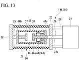
- FIG. 4 is a cross-sectional view showing the high voltage contact.
- a mechanical contact part 16 of the unitary switching part 14 constituting the high voltage contact 14A is a gas contact.
- the unitary switching part 14 constituting the high voltage contact 14A includes the mechanical contact part 16 having a fixed contact 17 and a movable contact 18, a sealed container 20 in which the mechanical contact part 16 and an insulating gas are enclosed, a fixed rod 25 connected to the fixed contact 17, an operation rod 26 connected to the movable contact 18, an operation mechanism 27 connected to the operation rod 26, and a capacitor 29 (refer to FIGS. 1 and 3 ) connected in parallel to the mechanical contact part 16.
- the mechanical contact part 16 is a contact having high withstand voltage performance.
- the fixed contact 17 and the movable contact 18 are provided to be brought into contact with or separated from each other.
- the mechanical contact part 16 is opened by separating the fixed contact 17 and the movable contact 18 from each other.
- a current conduction path which passes through the mechanical contact part 16 is opened by separating the fixed contact 17 and the movable contact 18 from each other.
- a direction in which the fixed contact 17 and the movable contact 18 are brought into contact with or separated from each other is referred to as a first direction.
- the first direction is one horizontal direction.
- the sealed container 20 encloses, for example, sulfur hexafluoride (SF 6 ) gas or the like as an insulating gas.
- the sealed container 20 includes a cylindrical insulated cylinder 21, and a first flange 22 and a second flange 23 which close openings at both ends of the insulated cylinder 21.
- the insulated cylinder 21 extends in the first direction.
- the insulated cylinder 21 is, for example, a bushing formed of an insulating material.
- Each of the first flange 22 and the second flange 23 is formed of a metal material.
- the fixing rod 25 is formed of a metal material.
- the fixing rod 25 extends in the first direction.
- the fixed rod 25 connects the first flange 22 with the fixed contact 17 in the sealed container 20.
- the fixed rod 25 may be integrally formed with the fixed contact 17.
- the fixed rod 25 electrically connects the fixed contact 17 to the first flange 22.
- the entire operation rod 26 is formed of a metal material.
- the operation rod 26 extends in the first direction.
- the operation rod 26 is connected to the movable contact 18 in the sealed container 20 and extends outside of the sealed container 20 through a through hole 23a provided in the second flange 23.
- the operation rod 26 may be integrally formed with the movable contact 18.
- the operation rod 26 is provided to be slidable with respect to the second flange 23 while keeping the inside of the sealed container 20 airtight.
- the operation rod 26 electrically connects the movable contact 18 with the second flange 23.
- the operation mechanism 27 is a highly responsive electromagnetic actuator energized by a power source.
- the electromagnetic actuator may be, for example, an electromagnetic repulsion operation mechanism.
- the electromagnetic repulsion operation mechanism has a metal plate of a good conductor connected to the operation rod 26, and a coil installed to face the metal plate. When the electromagnetic repulsion operation mechanism is driven, a current is applied to the coil to generate an induced current for the metal plate in a reverse direction, and a repulsive force in the reverse direction to the coil is applied to the metal plate to operate the operation rod 26.
- the operation mechanism 27 is disposed outside of the sealed container 20 to be parallel to the second flange 23 in the first direction.
- the operation mechanism 27 is fixed to the second flange 23 via a support portion 28.
- the entire support portion 28 is formed of a metal material.
- the operation mechanism 27 reciprocates the operation rod 26 in the first direction.
- the operation mechanism 27 displaces the movable contact 18 connected to the operation rod 26 and causes the movable contact 18 to be brought into contact with or separated from the fixed contact 17.
- the capacitor 29 is disposed outside of the sealed container 20.
- the capacitor 29 is connected to the first flange 22 and the second flange 23.
- the capacitor 29 is formed by encapsulating a dielectric in a high-resistance cylinder, and has electrodes at both ends thereof, and has capacitance and resistance.
- the capacitor 29 adjusts a voltage applied to the mechanical contact part 16 (refer to FIG. 4 ) at the time of current interruption and in an open state.
- FIG. 5 is a cross-sectional view showing the current interrupting contact.
- a mechanical contact part 36 of the unitary switching part 14 constituting the current interrupting contact 14B is a vacuum interrupter.
- the unitary switching part 14 constituting the current interrupting contact 14B includes the mechanical contact part 36 which is a vacuum interrupter 44 having a fixed contact 37 and a movable contact 38, a sealed container 40 which encloses the mechanical contact part 36, a fixed rod 45 connected to the fixed contact 37, an operation rod 46 connected to the movable contact 38, an operation mechanism 47 connected to the operation rod 46, and a capacitor 49 (refer to FIGS. 1 and 3 ) connected in parallel to the mechanical contact part 36.
- the mechanical contact part 36 is a contact capable of mechanically interrupting the current at a current zero point.
- the fixed contact 37 and the movable contact 38 are provided to be brought into contact with and separated from each other.
- the mechanical contact part 36 is opened by separating the fixed contact 37 and the movable contact 38 from each other.
- a current conduction path which passes through the mechanical contact part 36 is opened by separating the fixed contact 37 and the movable contact 38.
- a direction in which the fixed contact 37 and the movable contact 38 are brought into contact with and separated from each other is referred to as a second direction.
- the second direction is one horizontal direction.
- the vacuum interrupter 44 maintains an inside vacuum.
- the vacuum interrupter 44 includes the fixed contact 37, the movable contact 38, a cylindrical insulated cylinder 44a, a first flange 44b and a second flange 44c which close openings at both ends of the insulated cylinder 44a, and a bellows 44d provided at the inside of the insulated cylinder 44a.
- the insulated cylinder 44a extends in the second direction.
- the insulated cylinder 44a is, for example, a bushing formed of an insulating material.
- Each of the first flange 44b and the second flange 44c is formed of a metal material.
- the fixed contact 37 is connected to the first flange 44b in the vacuum interrupter 44.
- the fixed contact 37 is electrically connected with the first flange 44b.
- the movable contact 38 extends to the outside of the vacuum interrupter 44 through a through hole 44e provided in the second flange 44c.
- the movable contact 38 is provided to be slidable with respect to the second flange 44c.
- the movable contact 38 is electrically connected to the second flange 44c.
- the bellows 44d is disposed in the inside of the insulated cylinder 44a to surround the movable contact 38. One end portion of the bellows 44d is fixed to the second flange 44c. The other end portion of the bellows 44d is fixed to a peripheral surface of the movable contact 38.
- the bellows 44d isolates the vacuum in the vacuum interrupter 44 from the outside while causing the movable contact 38 to be displaceable with respect to the insulated cylinder 44a in the second direction.
- the sealed container 40 encloses, for example, sulfur hexafluoride (SF 6 ) gas or the like as an insulating gas.
- the sealed container 40 includes a cylindrical insulated cylinder 41, and a first flange 42 and a second flange 43 which close openings at both ends of the insulated cylinder 41.
- the insulated cylinder 41 extends in the second direction.
- the insulated cylinder 41 is, for example, a bushing formed of an insulating material.
- Each of the first flange 42 and the second flange 43 is formed of a metal material.
- the fixing rod 45 is formed of a metal material.
- the fixing rod 45 extends in the second direction.
- the fixed rod 45 connects the first flange 42 to the first flange 44b in the sealed container 40.
- the fixed rod 45 may be integrally formed with the first flange 44b.
- the fixed rod 45 electrically connects the fixed contact 37 to the first flange 44b and the first flange 42.
- the entire operation rod 46 is formed of a metal material.
- the operation rod 46 extends in the second direction.
- the operation rod 46 is connected to the movable contact 38 in the sealed container 40 and extends to the outside of the sealed container 40 through a through hole 43a provided in the second flange 43.
- the operation rod 46 may be integrally formed with the movable contact 38.
- the operation rod 46 is provided to be slidable with respect to the second flange 43.
- the operation rod 46 electrically connects the movable contact 38 with the second flange 43.
- the operation mechanism 47 is a highly responsive electromagnetic actuator energized by a power source.
- the electromagnetic actuator is, for example, an electromagnetic repulsion operation mechanism.
- the electromagnetic repulsion operation mechanism has a metal plate of a good conductor connected to the operation rod 46, and a coil installed to face the metal plate. When the electromagnetic repulsion operation mechanism is driven, a current is applied to the coil to generate an induced current to the metal plate in a reverse direction, and a repulsive force in the reverse direction to the coil is applied to the metal plate to operate the operation rod 46.
- the operation mechanism 47 is disposed outside of the sealed container 40 to be parallel to the second flange 43 in the second direction.
- the operation mechanism 47 is fixed to the second flange 43 via a support portion 48.
- the entire support portion 48 is formed of a metal material.
- the operation mechanism 47 reciprocates the operation rod 46 in the second direction.
- the operation mechanism 47 displaces the movable contact 38 connected to the operation rod 46 and causes the movable contact 38 to be brought into contact with or separated from the fixed contact 37.
- the capacitor 49 is disposed outside of the sealed container 40.
- the capacitor 49 is connected to the first flange 42 and the second flange 43.
- the capacitor 49 is formed by encapsulating a dielectric in a high-resistance cylinder, and has electrodes at both ends thereof, and has capacitance and resistance.
- the capacitor 49 adjusts a voltage applied to the mechanical contact part 36 (refer to FIG. 5 ) at the time of current interruption and in an open state.
- the pair of unitary switching parts 14 disposed on the mechanical switching part support plate 33 are disposed so that the respective operation rods 26, 46 are operated on the same straight line when the mechanical contact parts 16, 36 are opened by the operation mechanisms 27, 47.
- the operation rods 26, 46 of the respective unitary switching parts 14 extend on the same straight line.
- the pair of unitary switching parts 14 disposed on the mechanical switching part support plate 33 are disposed so that operating directions of the operation rods 26, 46 at the time of the opening operation of the mechanical contact parts 16, 36 by the operation mechanisms 27, 47 are opposite to each other.
- the pair of unitary switching parts 14 disposed on the mechanical switching part support plate 33 are disposed so that the respective operation mechanisms 27, 47 face each other and come into contact with each other. Further, the unitary switching part 14 of one mechanical switching unit 10 and the unitary switching part 14 of the other mechanical switching unit 10 are disposed to operate on the same straight line when seen in the vertical direction.
- the sealed containers 20, 40 of the pair of unitary switching parts 14 disposed on the mechanical switching part support plate 33 are disposed outside of the mechanical switching part support plate 33 in the horizontal direction.
- the whole of the sealed containers 20, 40 is disposed outside of the mechanical switching part support plate 33 in the horizontal direction
- only a part of the sealed containers 20, 40 may be disposed outside of the mechanical switching part support plate 33 in the horizontal direction.
- portions (for example, the first flanges 22, 42) of the sealed containers 20, 40 having the same potential as that of the fixed contacts 17, 37 may be disposed outside of the mechanical switching part support plate 33 in the horizontal direction.
- the above-described first direction is a projection line
- At least a part of the sealed containers 20, 40 may be disposed to protrude from a space (a space on the side on which the operation mechanisms 27, 47 are present) divided by the two vertical projection planes.
- the mechanical contact parts 16, 36 are electrically insulated from the ground.
- the operation mechanisms 27, 47 are provided at the same potential as that of the movable contacts 18, 38 of the mechanical contact parts 16, 36 and the mechanical switching part support plate 33.
- the operation mechanisms 27, 47 are provided such that a reference potential is the same potential as that of the movable contacts 18, 38 of the mechanical contact parts 16, 36 and the mechanical switching part support plate 33.
- the sealed containers 20, 40 are electrically insulated from the ground. Further, the sealed containers 20, 40 electrically insulate the fixed contacts 17, 37 from the movable contacts 18, 38 when the mechanical contact parts 16, 36 are opened.
- the power supply part 30 supplies power to the operation mechanisms 27, 47 of the pair of unitary switching parts 14 disposed on the mechanical switching part support plate 33 common to the power supply part 30.
- the power supply part 30 is provided so that a reference potential is the same as that of the operation mechanisms 27, 47.
- the power supply part 30 includes, for example, a capacitor which supplies power to the operation mechanisms 27, 47 at an opening operation of the mechanical contact parts 16, 36 (refer to FIGS.
- a capacitor which supplies power to the operation mechanisms 27, 47 at the time of a closing operation of the mechanical contact parts 16, 36, a charging device for the respective capacitors, and a switching element which holds each of the capacitors in a charged state and discharges power when the power is supplied (all of which are not shown).
- a power feeding device capable of supplying power while electrically insulating the power supply part 30 from the ground, such as an insulation transformer, a laser power feeding device, and an electromagnetic induction type wireless power feeding device (all of which are not shown), may be used for power supply from the ground to the charging device.
- the control part 31 monitors a state of the power supply part 30 and the operation mechanisms 27, 47 disposed on the same mechanical switching part support plate 33. Further, the control part 31 controls the power supply from the power supply part 30 disposed on the same mechanical switching part support plate 33 to the operation mechanisms 27, 47.
- the mechanical switching part support plate 33 is formed of a metal material such as an aluminum alloy.
- the mechanical switching part support plate 33 is formed in a rectangular shape in a plan view.
- the mechanical switching part support plates 33 are stacked in multiple stages in the vertical direction with respect to the insulating column 12.
- the mechanical switching part support plates 33 are installed in parallel in a direction (the first direction) in which the unitary switching parts 14 perform the interrupting operation.
- the insulating column 12 is formed of, for example, an insulator, a polymer, fiber reinforced plastic, or the like.
- the insulating column 12 stands on the foundation 5.
- the insulating column 12 extends in the vertical direction.
- the respective insulating columns 12 supports corner portions of the respective mechanical switching part support plates 33 stacked in multiple stages.
- the insulating column 12 electrically insulates the plurality of mechanical switching units 10 from each other and mechanically connects each of the mechanical switching units 10 to the foundation 5 while electrically insulating the mechanical switching units 10 from the foundation 5.
- the length of the insulating column 12 is set to insulate mechanical switching units 10 adjacent to each other in the vertical direction when the power is interrupted, and to electrically insulate all of the mechanical switching units 10 from the ground when power is applied. That is, the length of a portion of the insulating column 12 provided between a pair of mechanical switching units 10 adjacent to each other in the vertical direction is set so that the mechanical switching units 10 can be electrically insulated from each other when the power is interrupted. Further, the length of a portion of the insulating column 12 provided between the lowermost mechanical switching unit 10 and the foundation 5 is set so that all of the plurality of mechanical switching units 10 can be electrically insulated from the ground when power is applied.
- the length of the portion of the insulating column 12 provided between the lowermost mechanical switching unit 10 and the foundation 5 is longer than the length of the portion thereof provided between a pair of mechanical switching units 10 adjacent to each other in the vertical direction. Further, the length of the portion of the insulating column 12 provided between the lowermost mechanical switching unit 10 and the foundation 5 is shorter than the sum of the lengths of the portions provided between a pair of mechanical switching units 10 adjacent to each other in the vertical direction.
- the respective insulating columns 12 may extend continuously from a lower end to an upper end, or may be divided into a plurality of pieces to sandwich each of the mechanical switching part support plates 33.
- FIG. 6 is a perspective view schematically showing the mechanical switching part according to the first embodiment.
- the pair of unitary switching parts 14 disposed on the mechanical switching part support plate 33 are illustrated as one unitary switching part 14.
- illustration of the power supply part 30 and the control part 31 of each of the mechanical switching units 10 is omitted.
- the pair of unitary switching parts 14 in each of the mechanical switching units 10 are connected in series by an intra-unit bus bar 51 which connects the second flanges 23, 43 to each other.
- the first flanges 22, 42 of the first unitary switching part 14 of the first mechanical switching unit 10 and the first flanges 22, 42 of the second unitary switching part 14 of the second mechanical switching unit 10 are connected in series by the inter-unit bus bar 52.
- the unitary switching parts 14 are connected in series by the inter-unit bus bars 52 which connects the first flanges 22 to each other and the first flanges 22, 42 to the unitary switching parts 14 of the mechanical switching units 10 adjacent to each other in the vertical direction. Therefore, the plurality of high voltage contacts 14A and the plurality of current interrupting contacts 14B are connected in series by the intra-unit bus bar 51 and the inter-unit bus bar 52 and thus form a mechanical contact module 34. In this constitution, all the high voltage contacts 14A are connected in series with each other. Further, all the current interrupting contacts 14B are connected in series with each other.
- a first connection point A1, a second connection point A2, and a third connection point A3 are formed in the mechanical contact module 34.
- the first connection point A1 is formed at one of both end portions of the mechanical contact module 34 in which the current interrupting contact 14B is provided.
- the second connection point A2 is formed at one of both end portions of the mechanical contact module 34 on the side opposite to the first connection point A1.
- the third connection point A3 is an electrical connection point between the high voltage contact 14A and the current interrupting contact 14B.
- the first connection point A1 and the second connection point A2 are connected to a direct-current transmission system.
- FIG. 7 is a perspective view showing the semiconductor switching part of the first embodiment.
- the semiconductor switching part 3 is provided on the foundation 5 to be parallel to the mechanical switching part 2.
- the semiconductor switching part 3 includes a plurality of (three in the illustrated example) semiconductor switching units 60 and a plurality of (four in the illustrated example) insulating columns 62 which support the semiconductor switching units 60.
- the plurality of semiconductor switching units 60 are stacked in multiple stages in the vertical direction with respect to the insulating column 62.
- Each of the semiconductor switching units 60 includes a pair of semiconductor modules 64, a surge absorber 68, and a semiconductor switching part support plate 70 on which the pair of semiconductor modules 64 and the surge absorber 68 are fixedly disposed.
- the semiconductor module 64 includes a semiconductor stack 65 in which a plurality of semiconductor elements 65a are connected in series, a diode 66 connected in parallel to the semiconductor stack 65, and an attached circuit 67 connected to the semiconductor stack 65.
- the semiconductor element 65a is, for example, an insulated gate bipolar transistor (IGBT), an injection enhanced gate transistor (IEGT), or the like.
- the semiconductor stack 65 and the diode 66 are connected in parallel so that forward directions in which the power is applied are opposite to each other.
- the attached circuit 67 includes a snubber circuit which equalizes voltage distribution of the plurality of semiconductor elements 65a of the semiconductor stack 65, and a gate unit which outputs a switching command to the semiconductor element 65a.
- the pair of semiconductor modules 64 are connected in series so that the forward directions of the respective semiconductor stacks 65 are opposite to each other.
- FIG. 8 is a perspective view schematically showing the semiconductor switching part of the first embodiment.
- the surge absorbers 68 are connected in parallel to a pair of semiconductor modules 64 disposed on the same semiconductor switching part support plate 70. A current temporarily flows to the surge absorber 68 in a state in which the pair of semiconductor modules 64 are interrupted. The surge absorber 68 converts the current into thermal energy.
- the semiconductor switching part support plate 70 is formed of an insulating material such as fiber reinforced plastic or a metal material such as an aluminum alloy.
- the semiconductor switching part support plate 70 is formed so that both ends of the semiconductor module 64 are insulated, both ends of the surge absorber 68 are insulated and the semiconductor module 64 and the surge absorber 68 can be supported by the insulating column 62.
- the semiconductor switching part support plate 70 is stacked in multiple stages in the vertical direction with respect to the insulating column 62.
- the insulating column 62 is formed of, for example, an insulator, a polymer, fiber reinforced plastic, or the like.
- the insulating column 62 stands on the foundation 5.
- the insulating column 62 extends in the vertical direction.
- the respective insulating columns 62 supports corner portions of the respective semiconductor switching part support plates 70 stacked in multiple stages.
- the insulating column 62 electrically insulates the plurality of semiconductor switching units 60 from each other and mechanically connects each of the semiconductor switching units 60 to the foundation 5 while electrically insulating the semiconductor switching units 60 from the foundation 5.
- the length of the insulating column 62 is set to insulate the semiconductor switching units 60 adjacent to each other in the vertical direction when the power is interrupted, and to electrically insulate the whole of the semiconductor switching units 60 from the ground when the power is applied. That is, the length of a portion of the insulating column 62 provided between the pair of semiconductor switching units 60 adjacent to each other in the vertical direction is set so that the semiconductor switching units 60 can be electrically insulated from each other when the power is interrupted. Further, the length of a portion of the insulating column 62 provided between the lowermost semiconductor switching units 60 and the foundation 5 is set so that the whole of the plurality of semiconductor switching units 60 can be electrically insulated from the ground when the power is applied.
- the length of the portion of the insulating column 62 provided between the lowermost semiconductor switching units 60 and the foundation 5 is longer than the length of the portion thereof provided between the pair of semiconductor switching units 60 adjacent to each other in the vertical direction. Further, the length of the portion of the insulating column 62 provided between the lowermost semiconductor switching units 60 and the foundation 5 is shorter than the sum of the lengths of the portions provided between the pair of semiconductor switching units 60 adjacent to each other in the vertical direction.
- the respective insulating columns 62 may extend continuously from a lower end to an upper end, or may be divided into a plurality of pieces to sandwich each of the semiconductor switching part support plates 70.
- the pair of semiconductor modules 64 in each of the semiconductor switching units 60 are regarded as one semiconductor module 64
- the plurality of semiconductor modules 64 are connected in series by a plurality of bus bar 72.
- the semiconductor modules 64 are connected in series by the bus bars 72 to the semiconductor modules 64 of the semiconductor switching units 60 adjacent to each other in the vertical direction.
- all the semiconductor modules 64 connected in series are referred to as a semiconductor module group.
- the first connection point B1 and the second connection point B2 are formed in a semiconductor switching unit module group.
- the first connection point B1 is formed at one end of the semiconductor switching part module group.
- the second connection point B2 is formed at the other end of the semiconductor switching module part group.
- FIG. 9 is a perspective view showing the commutation device of the first embodiment.
- the commutation device 4 includes a commutation circuit 80, a commutation reactor 86, a commutation device support plate 88 on which the commutation circuit 80 and the commutation reactor 86 are fixedly disposed, and an insulating column 90 which supports the commutation device support plate 88.
- FIG. 10 is a circuit diagram showing the commutation circuit.
- the commutation circuit 80 is a half bridge circuit constituted by connecting a pair of legs 82 formed by connecting a pair of semiconductor elements 82a in series, with a capacitor 84 in parallel.
- the semiconductor element 82a is, for example, an IGBT, an IEGT, or the like.
- a diodes 82b is connected in parallel to each of the semiconductor elements 82a so that forward directions in which the power is applied are opposite to each other.
- An attached circuit (not shown) including a snubber circuit which equalizes voltage distribution of the semiconductor elements 82a and a gate unit which outputs a switching command to the semiconductor element 82a is connected to the pair of legs 82.
- One commutation circuit 80 may be provided, or a plurality of commutation circuits may be connected in series. In the example shown in FIG. 1 , one commutation circuit 80 is provided.
- FIG. 11 is a perspective view schematically showing the commutation device of the first embodiment.
- the commutation reactor 86 is connected in series to the commutation circuit 80 via a bus bar 92.
- the commutation reactor 86 adjusts a discharge time of the capacitor 84 of the commutation circuit 80.
- a first connection point C1, a second connection point C2, and a third connection point C3 are formed in a series of circuits formed by the commutation circuit 80 and the commutation reactor 86.
- the first connection point C1 is an electrical connection point between the commutation circuit 80 and the commutation reactor 86.
- the second connection point C2 is formed at one of both end portions of the commutation reactor 86 on the side opposite to the first connection point C1.
- the third connection point C3 is formed at one of both end portions of the commutation circuit 80 on the side opposite to the first connection point C1.
- the commutation device support plate 88 is formed of an insulating material such as fiber reinforced plastic or a metal material such as an aluminum alloy.
- the commutation device support plate 88 is formed so that both ends of the commutation circuit 80 are insulated, the commutation circuit 80 is insulated from the commutation reactor 86 by the other than the bus bar 92, and the commutation circuit 80 and the commutation reactor 86 can be supported by the insulating column 90.
- the insulating column 90 is formed of, for example, an insulator, a polymer, or fiber reinforced plastic.
- the insulating column 90 stands on the foundation 5.
- the insulating column 90 extends in the vertical direction.
- the respective insulating columns 90 support corner portions of the commutation device support plate 88.
- the insulating column 90 mechanically connects the commutation device support plate 88 to the foundation 5 while electrically insulating the commutation device support plate 88 from the foundation 5.
- the length of the insulating column 90 is set so that the commutation circuit 80 and the commutation reactor 86 can be electrically insulated from the ground when the power is applied.
- the commutation device support plate 88 is disposed above the semiconductor switching part 3. Also, the insulating column 90 of the commutation device 4 is shared with the insulating column 62 of the semiconductor switching part 3. As a result, the commutation device 4 is stacked on an upper portion of the semiconductor switching part 3. In this case, the insulating column 90 electrically insulates the commutation circuit 80 and the commutation reactor 86 from the semiconductor switching unit 60.
- the length of a portion of the insulating column 90 provided between the commutation device support plate 88 and the semiconductor switching unit 60 disposed immediately below the commutation device support plate 88 is set so that the commutation circuit 80 and the commutation reactor 86 can be electrically insulated from the semiconductor switching unit 60 when the power is interrupted.
- FIG. 12 is a circuit diagram schematically showing the direct-current circuit breaker of the first embodiment.
- a plurality of high voltage contacts 14A connected in series with each other are illustrated as one high voltage contact 14A.
- the pair of current interrupting contacts 14B connected in series with each other are illustrated as one current interrupting contact 14B.
- FIG. 12 shows only a pair of semiconductor modules 64 connected in series among the plurality of semiconductor modules 64 connected in series.
- a series of circuits formed by the commutation circuit 80 and the commutation reactor 86 are connected in parallel to the current interrupting contact 14B.
- the commutation circuit 80 is connected to the high voltage contact 14A side from the commutation reactor 86.
- the second connection point C2 of the commutation device 4 and the first connection point A1 of the mechanical contact module 34 are electrically connected by a bus bar 94.
- the third connection point C3 of the commutation device 4 and the third connection point A3 of the mechanical contact module 34 are electrically connected by a bus bar 95.
- the semiconductor module 64 is connected in parallel to a series of circuits formed by the high voltage contact 14A and the commutation circuit 80. Specifically, the first connection point B1 of the semiconductor switching part 3 and the second connection point A2 of the mechanical contact module 34 are electrically connected by a bus bar 96. In addition, the second connection point B2 of the semiconductor switching part 3 and the first connection point C1 of the commutation device 4 are electrically connected by a bus bar 97.
- a transmission current flows to the mechanical contact module 34. In this state, no current flows to the semiconductor module 64, the commutation circuit 80, and the commutation reactor 86. Further, the capacitor 84 of the commutation circuit 80 is charged in advance by a power feeding device (not shown) capable of supplying power while electrically insulating the ground and the commutation circuit 80 from each other.
- the semiconductor element 82a of the commutation circuit 80 is turned on (a power applied state), and an electric charge of the capacitor 84 is discharged.
- a current of the current interrupting contact 14B connected in parallel to the commutation circuit 80 decreases, and a current zero point is generated at the current interrupting contact 14B. Therefore, an arc is extinguished at the current interrupting contact 14B, and the commutation is completed.
- the fault current flows through the high voltage contact 14A, the commutation circuit 80 and the commutation reactor 86.
- the semiconductor element 65a of the semiconductor module 64 is turned on, and the semiconductor element 82a of the commutation circuit 80 is switched off.
- the fault current is commutated to the semiconductor module 64 connected in parallel to the commutation circuit 80.
- the fault current flows through the semiconductor module 64 and the commutation reactor 86.
- the semiconductor element 65a of the semiconductor module 64 is switched off.
- the fault current is commutated to the surge absorber 68 connected in parallel to the semiconductor element 65a.
- the fault current is absorbed in the surge absorber 68, and the interruption of the fault current in the direct-current transmission system is completed.
- the mechanical switching part 2 has the unitary switching part 14 including the mechanical contact parts 16, 36 which have the fixed contacts 17, 37 and the movable contacts 18, 38 and are electrically insulated from the ground, the sealed containers 20, 40 which enclose the mechanical contact parts 16, 36 and an insulating gas and are electrically insulated from the ground, the operation rods 26, 46 connected to the movable contacts 18, 38, and the operation mechanisms 27, 47 connected to the operation rods 26, 46 and provided at the same potential as the movable contacts 18, 38 of the mechanical contact parts 16, 36 is adopted.
- the sealed containers 20, 40 are not grounded to the ground, the insulation between the sealed containers 20, 40 and the mechanical contact parts 16, 36 can be omitted. Therefore, the sealed containers 20, 40 can be downsized, and an increase in size of the unitary switching part 14 can be curbed as compared with a case in which the sealed container is electrically insulated from the mechanical contact part by being grounded to the ground, or the like. Further, even when the plurality of unitary switching parts 14 are connected in series to improve the interrupting performance as the voltage is increased, the increase in size of all the unitary switching parts 14 connected in series can be curbed. Accordingly, it is possible to provide the direct-current circuit breaker 1 which is easy to increase the voltage and can curb the increase in size.
- the insulation of the operation rods 26, 46 interposed between the mechanical contact parts 16, 36 and the operation mechanisms 27, 47 can be omitted, and an increase in length of the operation rods 26, 46 can be curbed as compared with a case in which the operation mechanism is electrically insulated from the mechanical contact part by being grounded to the ground, or the like.
- an increase in mass of the mobile parts of the operation mechanisms 27, 47 is curbed, and a decrease in the opening speed of the mechanical contact parts 16, 36 can be curbed. Therefore, it is possible to provide the direct-current circuit breaker 1 capable of securing responsiveness of the interrupting operation.
- each of the mechanical switching units 10 are disposed so that the respective operation rods 26, 46 operate on the same straight line by the operation mechanisms 27, 47, and the operating directions of the operation rods 26, 46 by the operation mechanisms 27, 47 are opposite to each other.
- the pair of unitary switching parts 14 disposed on the mechanical switching part support plate 33 are disposed so that the respective operation mechanisms 27, 47 face each other and come into contact with each other.
- the sealed containers 20, 40 of the pair of unitary switching parts 14 disposed on the mechanical switching part support plate 33 is disposed outside of the mechanical switching part support plate 33 in the horizontal direction.
- the mechanical switching part support plate 33 is formed of a metal material.
- the movable contacts 18, 38 of the mechanical contact parts 16, 36, the operation mechanisms 27, 47, and the mechanical switching part support plate 33 are provided at the same potential.
- the plurality of mechanical switching units 10 are stacked in multiple stages with respect to the insulating column 12, an installation area of the direct-current circuit breaker 1 can be reduced as compared with the case in which the mechanical switching units are disposed side by side.
- the same operation and effect can be obtained also in that the plurality of semiconductor switching units 60 are stacked in multiple stages with respect to the insulating column 62. Further, the same operation and effect can be obtained also in that the commutation device 4 is stacked on the upper portion of the semiconductor switching part 3.
- each of the plurality of mechanical switching units 10 at least a part of the sealed containers 20, 40 of each of the pair of unitary switching parts 14 are disposed outside of the mechanical switching part support plate 33 in the horizontal direction.
- the bus bar 52 may also be installed with a sufficient insulation distance from the mechanical switching part support plate 33.
- the operation mechanisms 27, 47 of the pair of unitary switching parts 14 disposed on the mechanical switching part support plate 33 are disposed to be opposed to and in contact with each other. Therefore, when the operation rods 26, 46 are operated, the impact force and the reaction generated in the operation mechanisms 27, 47 can be offset more effectively.
- both of the pair of unitary switching parts 14 disposed on the mechanical switching part support plate 33 constitute only one of the high voltage contact 14A and the current interrupting contact 14B. Therefore, when the operation rods 26, 46 in the pair of unitary switching parts 14 are operated, the impact force and the reaction generated in the operation mechanisms 27, 47 can be made equal to each other. Thus, the impact force and the reaction can be offset more effectively.
- the operation mechanisms 27, 47 are disposed outside of the sealed containers 20, 40. Therefore, maintainability of the operation mechanisms 27, 47 can be improved as compared with a case in which the operation mechanism is disposed in the inside of the sealed container.
- the mechanical contact part 16 of the unitary switching part 14 constituting the high voltage contact 14A is a gas contact
- the present invention is not limited thereto.
- the mechanical contact part 36 of the unitary switching part 14 constituting the high voltage contact 14A may be a vacuum interrupter having a withstand voltage performance equivalent to that of the mechanical contact part 16 in the first embodiment.
- the pair of current interrupting contacts 14B are provided in the mechanical switching part 2, the present invention is not limited thereto. At least one current interrupting contact 14B may be provided in the mechanical switching part 2.
- the uppermost mechanical switching unit 10 may include both the high voltage contact 14A and the current interrupting contact 14B.
- the pair of unitary switching parts 14 are preferably disposed so that the respective operation rods 26, 46 operate on the same straight line by the operation mechanisms 27, 47 and the operating directions of the operation rods 26, 46 by the operation mechanisms 27, 47 are opposite to each other.
- high voltage contacts 14A are provided in the mechanical switching part 2, the invention is not limited thereto. At least one high voltage contact 14A may be provided in the mechanical switching part 2.
- FIG. 14 is a front view schematically showing a mechanical switching part according to a second embodiment.
- illustration of the power supply part 30 and the control part 31 (refer to FIGS. 1 and 3 ) of each of the mechanical switching unit 10 is omitted.
- the second embodiment shown in FIG. 14 is different from the first embodiment in that the current interrupting contact 14B is disposed so that the operating direction of the operation rod 46 by the operation mechanism 47 follows an extending direction (that is, the vertical direction) of the insulating column 12.
- the uppermost mechanical switching unit 10 includes one current interrupting contact 14B, the power supply part and the control part which are not shown, and the mechanical switching part support plate 33 on which the current interrupting contact 14B (the unitary switching part 14), the power supply part and control part are fixedly disposed.
- the current interrupting contact 14B is placed longitudinally. That is, the current interrupting contact 14B is disposed so that the above-described second direction follows the vertical direction.
- the operation rod 46 is disposed to extend in the vertical direction.
- the operation mechanism 47 is located between the sealed container 40 and the mechanical switching part support plate 33 and is fixed to the mechanical switching part support plate 33.
- the mechanical switching units 10 are stacked in two stages, the present invention is not limited thereto, and the mechanical switching units 10 may be stacked in three or more stages.
- the present invention is not limited thereto, and the high voltage contact 14A may be disposed longitudinally.
- FIG. 15 is a front view schematically showing a mechanical switching part according to a third embodiment.
- illustration of the power supply part 30 and the control part 31 (refer to FIGS. 1 and 3 ) of a mechanical switching unit 110 is omitted.
- the third embodiment as shown in FIG. 15 is different from the above-described embodiments in that the pair of unitary switching parts 14 are directly supported by the insulating column 12.
- the mechanical switching unit 110 includes the pair of unitary switching parts 14, the power supply part and the control unit which are not shown, and a connection member 53 which connects the high voltage contact 14A with the current interrupting contact 14B.
- the first unitary switching part 14 constitutes the high voltage contact 14A.
- the second unitary switching part 14 constitutes the current interrupting contact 14B.
- the high voltage contact 14A and the current interrupting contact 14B are longitudinally disposed on the insulating column 12.
- the high voltage contact 14A is fixedly disposed on the insulating column 12 so that the above-described first direction follows the vertical direction.
- the operation rod 26 is disposed to extend in the vertical direction.
- the operation mechanism 27 is located between the sealed container 20 and an upper end portion of the insulating column 12 and is fixed to the insulating column 12. Further, the current interrupting contact 14B is fixedly disposed on the insulating column 12 so that the above-described second direction follows the vertical direction.
- the operation rod 46 is disposed to extend in the vertical direction.
- the operation mechanism 47 is located between the sealed container 40 and the upper end portion of the insulating column 12 and is fixed to the insulating column 12.
- connection member 53 is formed of a conductive metal material or the like.
- the connection member 53 is disposed between the high voltage contact 14A and the current interrupting contact 14B.
- the connection member 53 mechanically and electrically connects the second flange 23 of the unitary switching part 14 constituting the high voltage contact 14A with the second flange 43 of the unitary switching part 14 constituting the current interrupting contact 14B.
- the pair of unitary switching parts 14 are electrically connected in series to each other and mechanically fixed to each other.
- the vibration of the mechanical switching part having the mechanical switching unit 110 can be curbed, and the excessive increase in size of the insulating column 12, the increase of the number of supporting structures, and the increase in weight thereof can be curbed.
- the vibration of the mechanical switching part having the mechanical switching unit 110 can be curbed more reliably.
- both of the pair of unitary switching parts 14 directly supported by the insulating column 12 may constitute the high voltage contact 14A, and both of the pair of unitary switching parts 14 may constitute the current interrupting contact 14B.
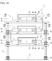
- FIG. 16 is a front view schematically showing a mechanical switching part according to a fourth embodiment.
- illustration of the power supply part 30 and the control part 31 (refer to FIGS. 1 and 3 ) of the mechanical switching unit 10 is omitted.
- the fourth embodiment as shown in FIG. 16 is different from the above-described embodiments in that the insulating column 12 has a damping member 54 which absorbs vibration.
- the damping member 54 is disposed at the insulating column 12 between the mechanical switching part support plates 33 of the mechanical switching units 10 adjacent to each other in the vertical direction and at the insulating column 12 between the mechanical switching part support plate 33 of the lowermost mechanical switching unit 10 and the foundation 5.
- the damping members 54 are respectively disposed at a connecting portion between the foundation 5 and the insulating column 12 and a connecting portion between an upper surface of each of the mechanical switching part support plates 33 and the insulating column 12.
- the damping member 54 absorbs the vibration transmitted through the insulating column 12.
- the damping member 54 is, for example, an air damper (an air spring) in which a bellows-shaped rubber member containing air is sandwiched between metal plates, an anti-vibration rubber, or the like.
- the vibration generated by the mechanical switching unit 10 is absorbed by the damping member 54.
- the vibration generated in the mechanical switching unit 10 is absorbed by the damping member 54.
- the damping member 54 since a force in a bending direction of the insulating column 12 can be absorbed by the damping member 54, the generation of the bending moment in the insulating column 12 can be curbed. Therefore, the vibration of the mechanical switching part 2 can be curbed, and the excessive increase in size of the insulating column 12, the increase in the number of supporting structures, and the increase in weight thereof can be curbed.
- the damping members 54 are respectively disposed at the connecting portion between the foundation 5 and the insulating column 12 and the connecting portion between the upper surface of each of the mechanical switching part support plates 33 and the insulating column 12, the present invention is limited thereto.
- the damping members may be disposed at a connection portion between a lower surface of each of the mechanical switching part support plates 33 and the insulating column 12.
- FIG. 17 is a front view schematically showing a mechanical switching part according to a fifth embodiment.
- illustration of the power supply part 30 and the control part 31 (refer to FIGS. 1 and 3 ) of the mechanical switching unit 10 is omitted.
- the fifth embodiment as shown in FIG. 17 is different from the above-described embodiments in that the insulating column 12 is hung on the ceiling of a building 6.
- the direct-current circuit breaker 1 is installed in the building 6 in consideration of the maintainability, an influence of contamination, or the like.
- the respective wall portions which constitutes the building 6 is provided at a position which maintains an insulation distance with respect to a high voltage part of the direct-current circuit breaker 1.
- the insulating column 12 is hung on the ceiling of the building 6.
- the insulating column 12 has a joint 56 and supports the mechanical switching unit 10 in a rockable manner with respect to the building 6.
- the joint 56 is provided in a connecting portion between the insulating column 12 and the ceiling of the building 6 and a connecting portion between the insulating column 12 and the upper and lower surfaces of the mechanical switching part support plate 33.
- the length of the insulating column 12 is set to be able to electrically insulate the mechanical switching units 10 adjacent to each other in the vertical direction when the power is interrupted and also to electrically insulate the whole of the mechanical switching unit 10 from the ground and the building 6 when the power is applied. That is, the length of a portion of the insulating column 12 provided between the mechanical switching unit 10 located uppermost and the ceiling of the building 6 is set to electrically insulate the whole of the mechanical switching unit 10 from the building 6 when the power is applied. Further, the entire length of the insulating column 12 is set to electrically insulate the entire mechanical switching unit 10 from the foundation 5 when the power is applied.
- the insulating column 12 supports each of the mechanical switching units 10 from the upper side, even when a force in the bending direction of the mechanical switching unit 10 acts on the insulating column 12 from the mechanical switching unit 10, the force in the bending direction can be offset by the gravity of the mechanical switching unit 10. Therefore, as compared to the constitution in which each of the insulating column 12 is supported from the lower side, the occurrence of the bending moment in the insulating column 12 can be curbed more reliably.
- the vibration of the mechanical switching part 2 can be curbed, and the excessive increase in size of the insulating column 12, the increase in the number of supporting structures, and the increase in weight thereof can be curbed.
- the insulating column 12 supports the mechanical switching units 10 in a rockable manner with respect to the building 6, even when the building 6 is vibrated due to an earthquake or the like, the transmission of the vibration of the building 6 to the mechanical switching units 10 can be reduced by rocking the mechanical switching units 10 with respect to the building 6. Accordingly, the vibration of the mechanical switching part 2 can be curbed, and the excessive increase in size of the insulating column 12, the increase in the number of supporting structures, and the increase in weight thereof can be curbed.
- the insulating column 62 of the semiconductor switching part 3 and the insulating column 90 of the commutation device 4 may also be hung on the ceiling of the building 6. Accordingly, the same operation and effect as those in the case in which the insulating column 12 of the mechanical switching part 2 is hung on the ceiling of the building 6 can be achieved.
- the present invention is not limited thereto.
- the plurality of mechanical switching units 10 may be disposed in parallel in the horizontal direction while being supported by the insulating columns 12.
- the mechanical switching part support plate 33, the semiconductor switching part support plate 70, and the commutation device support plate 88 are formed separately from each other, the present invention is not limited thereto and may be constituted to share each other. That is, the mechanical switching part support plate 33 may be integrated with at least one of the semiconductor switching part support plate 70 and the commutation device support plate 88. In this case, since the vibration of the mechanical switching part 2 is curbed as described above, the vibration of the semiconductor switching part 3 and the commutation device 4 due to the opening operation of the mechanical switching part 2 is curbed.
- the mechanical switching part 2 is disposed in parallel to the semiconductor switching part 3 and the commutation device 4, the present invention is not limited thereto.
- the mechanical switching unit 10 may be stacked on the semiconductor switching unit 60 by sharing the insulating column 12 of the mechanical switching part 2 and the insulating column 62 of the semiconductor switching part 3.
- a ground area of the direct-current circuit breaker can be reduced.
- the vibration of the mechanical switching part 2 is curbed, the vibration of the semiconductor switching part 3 and the commutation device 4 due to the opening operation of the mechanical switching part 2 is curbed.
- some of the operation rods and the support portions may be formed of an insulating material or a high resistance material. Also, in this case, since a potential difference between the movable contacts 18, 38 and the operation mechanisms 27, 47 is small, the insulating portion can be made small, and the increase in length of the operation rod can be curbed as compared with a case in which the operation mechanism is electrically insulated from the mechanical contact part by being grounded on the ground, or the like.
- an insulating material may be interposed between the operation mechanisms 27, 47 disposed on the same mechanical switching part support plate 33 and between the operation mechanisms 27, 47 and other members to electrically insulate them from each other.
- the current conduction paths from the operation mechanisms 27, 47 to other members other than the movable contacts 18, 38 are eliminated, the power application from the movable contacts 18, 38 to the operation mechanisms 27, 47 can be curbed.
- a shield which alleviates concentration of an electric field may be appropriately installed in the mechanical switching part 2, the semiconductor switching part 3 and the commutation device 4 in each of the above-described embodiments.
- the shield may be installed at an end portion of the unitary switching part 14 or end portions of the mechanical switching part support plate 33, the semiconductor switching part support plate 70, and the commutation device support plate 88 which are likely to cause the concentration of the electric field.
- a distance required to electrically insulate the respective portions of the mechanical switching part 2, the semiconductor switching part 3, and the commutation device 4 can be shortened, and the increase in size of the direct-current circuit breaker 1 can be curbed. Accordingly, it is possible to provide a direct-current circuit breaker capable of increasing the voltage and curbing the increase in size.
- the mechanical switching part support plate 33 is formed of a metal material, the present invention is not limited thereto.
- the mechanical switching part support plate may be formed of an insulating material such as fiber reinforced plastic.
- a mechanical switching part includes a mechanical switching unit having one pair of unitary switching parts including a mechanical contact part having a fixed contact and a movable contact and electrically insulated from the ground, a sealed container which encloses the mechanical contact part and an insulating gas and is electrically insulated from the ground, an operation rod connected to the movable contact, and an operation mechanism connected to the operation rod and provided at the same potential as that of the movable contact of the mechanical contact part; and an insulating column which supports the mechanical switching unit.
- the mechanical switching unit further includes a mechanical switching part support plate on which the pair of unitary switching parts are disposed and which is supported by the insulating column.
- the pair of unitary switching parts are disposed so that each of the operation rods is operated on the same straight line by the operation mechanism, operating directions of the operation rods by the operation mechanism are opposite to each other, and each of the operation mechanisms is disposed to face each other.
Landscapes
- Engineering & Computer Science (AREA)
- Power Engineering (AREA)
- Driving Mechanisms And Operating Circuits Of Arc-Extinguishing High-Tension Switches (AREA)
- Gas-Insulated Switchgears (AREA)
Abstract
Description
- The present invention relates to a direct-current circuit breaker, a mechanical switching device for a direct-current circuit breaker, and a semiconductor switching device for a direct-current circuit breaker.
- Direct-current power transmission has higher power transmission efficiency than alternating-current power transmission. On the other hand, the introduction costs of equipment for direct-current power transmission is higher than that for alternating-current transmission. However, in long-distance power transmission, underwater power transmission, or the like, since the power transmission efficiency of direct-current power transmission is overwhelmingly high, direct-current power transmission generally has lower costs when this is evaluated by adding operating costs to the equipment costs. Therefore, direct-current power transmission is used, for example, for power transmission between two bases across the sea. In recent years, a method in which large-scale power generation is performed at a location far from an urban area that is a major power consumer using offshore wind power generation or solar power generation in a desert area or the like and then long-distance power transmission is performed has been studied to enhance a proportion of power generated using renewable energy in all generated power and to supply a larger amount of power using renewable energy. Accordingly, construction of direct-current power transmission networks which connect a plurality of power supply points with a plurality of demand points is planned.
- When a power transmission network in which three or more bases are connected with each other is constructed, a device capable of rapidly isolating a point at which an accident has occurred from a healthy system is required when an accident occurs in the power transmission network. In general, a mechanical contact type circuit breaker is used in an alternating current system. A mechanical contact type circuit breaker opens contacts at a current zero point generated by an alternating current and interrupts a fault current by blowing an insulating medium with an arc current between the contacts. On the other hand, in a direct-current transmission system, since a current zero point does not occur in a fault current, it is thought that it would be difficult to quickly interrupt a fault current in a conventional mechanical contact type circuit breaker.
- Therefore, a semiconductor circuit breaker using a plurality of semiconductor elements having a self-extinguishing capability, such as insulated gate bipolar transistors (IGBTs), has been proposed as a semiconductor breaker capable of interrupting a direct current alone. However, since all of the power to be transmitted always passes through the plurality of semiconductor elements, a large conduction loss occurs, and thus a decrease in the power transmission efficiency is caused during a normal operation.
- To solve this problem, a hybrid circuit breaker in which another semiconductor circuit breaker is connected in parallel to a circuit in which a mechanical contact type disconnector and an auxiliary semiconductor circuit breaker are connected in series has been proposed. In the hybrid circuit breaker, when power is transmitted normally, the mechanical contact type disconnector and the auxiliary semiconductor circuit breaker are in a conductive state, and the other semiconductor circuit breaker is in an interrupted state. Thus, a transmission current flows through the mechanical contact type disconnector and the auxiliary semiconductor circuit breaker.
- Also, in the event of an accident, an opening command is given to the mechanical contact type disconnector at the same time as the auxiliary semiconductor circuit breaker is put into an interrupted state. In this way, since the auxiliary semiconductor circuit breaker is in an interrupted state, a fault current flowing in a path between the mechanical contact type disconnector and the auxiliary semiconductor circuit breaker is commutated to the above-described other semiconductor circuit breaker. Additionally, after the opening operation of the mechanical contact type disconnector is completed, and withstand voltage performance of a steady current conduction path is secured, the interruption of a fault current is completed by shutting off the other semiconductor circuit breaker.
- In such a hybrid circuit breaker, since the conduction loss at the time of steady energization is only the conduction loss in the auxiliary semiconductor circuit breaker, the conduction loss can be reduced as compared with a constitution in which the steady current conduction path is only in the semiconductor circuit breaker which can interrupt a direct current alone as described above. However, since the conduction loss in the auxiliary semiconductor circuit breaker still occurs, the hybrid circuit breaker has a large conduction loss as compared with a conventional mechanical contact type circuit breaker in which the steady current conduction path includes only the mechanical contacts.
- Therefore, a direct-current circuit breaker in which a mechanical contact type circuit breaker is connected in parallel to a circuit in which a semiconductor circuit breaker and a commutation circuit constituted by a half bridge circuit are connected in series has been proposed. In this direct-current circuit breaker, when power is transmitted normally, the mechanical contact type disconnector is in a conductive state, and the semiconductor circuit breaker and the commutation circuit are in an interrupted state. Therefore, when power is transmitted normally, the transmission current flows only through the mechanical contact type disconnector.
- In the event of an accident, an opening command is given to the mechanical contact type circuit breaker, the semiconductor circuit breaker is brought into a conductive state, and a commutation command is given to the commutation circuit. Then, the commutation circuit generates a zero point in the current of the mechanical contact type circuit breaker by causing a current to flow in a direction opposite to a fault current flowing to the mechanical contact type circuit breaker, and the fault current is commutated from the mechanical contact type circuit breaker to the semiconductor circuit breaker and the commutation circuit by the mechanical contact type circuit breaker opening. After the commutation of the fault current, interruption of the fault current is completed by shutting off the semiconductor circuit breaker.
- In such a direct-current circuit breaker, since the steady current conduction path is formed only by the mechanical contact type circuit breaker, it is possible to significantly reduce the conduction loss.
- A general mechanical contact type circuit breaker includes a fixed contact and a mobile contact which are provided to be brought into contact with or separated from each other, a metal tank which encloses the fixed contact and the mobile contact therein, and an operation mechanism which is driven so that the mobile contact is brought into contact with or separated from the fixed contact. The inside of the metal tank is filled with an insulating medium. The metal tank is grounded and electrically insulated from the fixed contact and the mobile contact. The operation mechanism is grounded and located outside of the metal tank and is connected to the mobile contact in the metal tank via a seal rod which passes through the metal tank and an insulating operation rod which is connected to the seal rod in the metal tank.
- However, it is necessary to improve the withstand voltage performance in the respective parts of the mechanical contact type circuit breaker as a voltage of the direct-current transmission system increases. That is, in the above-described mechanical contact type circuit breaker, it is necessary to increase a distance between the fixed contact and the mobile contact in the high voltage part and the grounded metal tank to electrically insulate them from each other, as the voltage is increased. Further, when desired interrupting performance cannot be obtained with one mechanical contact type circuit breaker as the voltage is increased, a plurality of mechanical contact type circuit breakers may be connected in series to improve the interrupting performance. Also in this case, in all the mechanical contact type circuit breakers connected in series, it is necessary to increase the distance between the fixed contact and the mobile contact of the high voltage part and the grounded metal tank to electrically insulate them from each other. As a result, a size of the mechanical contact type circuit breaker increases. The direct-current circuit breaker is assumed to be operated on a platform built on the sea, and the cost of building the platform may increase due to the increase in the size of the mechanical contact type circuit breaker. Further, as the voltage is increased, an insulating rod which connects the mobile contact of the high voltage part with the grounded operation mechanism is also elongated. As a result, since a mass of a movable part of the operation mechanism increases, an opening speed of the fixed contact and the mobile contact may be reduced, and responsiveness of the interrupting operation may be reduced.
-
- [Patent Document 1]
Japanese Unexamined Patent Application, First Publication No.2016-187275 - [Patent Document 2]
PCT International Publication No. WO 2011/057675 - [Patent Document 3]
PCT International Publication No. WO 2013/131582 - An object of the present invention is to provide a direct-current circuit breaker capable of easily increasing a voltage, curbing an increase in a size thereof, and ensuring responsiveness of an interrupting operation, a mechanical switching device for a direct-current circuit breaker, and a semiconductor switching device for a direct-current circuit breaker.
- A direct-current circuit breaker of an embodiment includes a mechanical switching part, a semiconductor switching part, and a commutation device. The mechanical switching part includes at least one mechanical switching unit, and an insulating column which supports the at least one mechanical switching unit. The mechanical switching unit has at least one unitary switching part. The unitary switching part includes a mechanical contact part, a sealed container, an operation rod, and an operation mechanism. The mechanical contact part has a fixed contact and a movable contact. The mechanical contact part is electrically insulated from the ground. The sealed container encloses the mechanical contact part and an insulating gas. The sealed container is electrically insulated from the ground. The operation rod is connected to the movable contact. The operation rod extends from an inside of the sealed container to outside thereof. The operation mechanism is connected to the operation rod. The operation mechanism causes the movable contact to be brought into contact with or separated from the fixed contact. The operation mechanism is provided at the same potential as that of the movable contact. The semiconductor switching part includes a semiconductor module and a surge absorber. The semiconductor module includes a semiconductor stack in which a plurality of semiconductor elements are connected in series. The surge absorber is connected in parallel to the semiconductor module. The commutation device includes a commutation circuit and a commutation reactor. The commutation circuit is constituted by connecting in parallel a pair of legs formed by connecting one pair of semiconductor elements in series with a capacitor. The commutation reactor is connected in series to the commutation circuit. The mechanical switching part includes a current interrupting contact, and a high voltage contact. The high voltage contact has a withstand voltage performance higher than or equivalent to that of the current interrupting contact. The at least one mechanical switching unit further includes a mechanical switching part support plate. The at least one unitary switching part is disposed on the mechanical switching part support plate. The mechanical switching part support plate is supported by the insulating column. The mechanical switching part support plate is provided at the same potential as that of the operation mechanism. The at least one unitary switching part includes a first unitary switching part and a second unitary switching part. The first unitary switching part constitutes one of the current interrupting contact and the high voltage contact. The second unitary switching part constitutes one of the current interrupting contact and the high voltage contact. The first unitary switching part and the second unitary switching part are disposed so that the respective operation rods are operated on the same straight line by the operation mechanism. The first unitary switching part and the second unitary switching part are disposed so that operating directions of the operation rods using the operation mechanism are opposite to each other. The first unitary switching part and the second unitary switching part are disposed so that the respective operation mechanisms face each other. At least a part of the sealed container of the first unitary switching part is disposed outside of the mechanical switching part support plate in a horizontal direction. At least a part of the sealed container of the second unitary switching part is disposed outside of the mechanical switching part support plate in a horizontal direction. The current interrupting contact and the high voltage contact are connected in series to form a mechanical contact module. Both ends of the mechanical contact module are connected to a direct-current transmission system. The commutation circuit and the commutation reactor are connected in parallel to the current interrupting contact. The commutation circuit is connected to the high voltage contact side from the commutation reactor. The semiconductor module is connected in parallel to the high voltage contact and the commutation circuit.
-
-
FIG. 1 is a perspective view showing a direct-current circuit breaker according to a first embodiment. -
FIG. 2 is a perspective view schematically showing the direct-current circuit breaker of the first embodiment. -
FIG. 3 is a perspective view showing a mechanical switching part according to the first embodiment. -
FIG. 4 is a cross-sectional view showing a high voltage contact. -
FIG. 5 is a cross-sectional view showing a current interrupting contact. -
FIG. 6 is a perspective view schematically showing the mechanical switching part according to the first embodiment. -
FIG. 7 is a perspective view showing a semiconductor switching part according to the first embodiment. -
FIG. 8 is a perspective view schematically showing the semiconductor switching part according to the first embodiment. -
FIG. 9 is a perspective view showing a commutation device according to the first embodiment. -
FIG. 10 is a circuit diagram showing the commutation circuit. -
FIG. 11 is a perspective view schematically showing the commutation device of the first embodiment. -
FIG. 12 is a circuit diagram schematically showing the direct-current circuit breaker of the first embodiment. -
FIG. 13 is a cross-sectional view showing a modified example of the high voltage contact. -
FIG. 14 is a front view schematically showing a mechanical switching part according to a second embodiment. -
FIG. 15 is a front view schematically showing a mechanical switching part according to a third embodiment. -
FIG. 16 is a front view schematically showing a mechanical switching part according to a fourth embodiment. -
FIG. 17 is a front view schematically showing a mechanical switching part according to a fifth embodiment. - Hereinafter, a direct-current circuit breaker, a mechanical switching device for a direct-current circuit breaker, and a semiconductor switching device for a direct-current circuit breaker according to an embodiment will be described with reference to the drawings. In the following description, components having the same or similar functions are designated by the same reference numerals. Additionally, duplicate explanation of the components may be omitted.
-
FIG. 1 is a perspective view showing a direct-current circuit breaker according to the first embodiment.FIG. 2 is a perspective view schematically showing the direct-current circuit breaker according to the first embodiment. - As shown in
FIGS. 1 and2 , the direct-current circuit breaker 1 includes a mechanical switching part 2 (a mechanical switching device), a semiconductor switching part 3 (a semiconductor switching device), and acommutation device 4. -
FIG. 3 is a perspective view showing the mechanical switching part according to the first embodiment. - As shown in
FIGS. 1 and3 , themechanical switching part 2 includes a plurality of (four in the illustrated example)mechanical switching units 10 and a plurality of (four in the illustrated example) insulatingcolumns 12 which support themechanical switching units 10. The plurality ofmechanical switching units 10 are stacked in multiple stages in the vertical direction with respect to the insulatingcolumns 12. - Each of the
mechanical switching units 10 includes a pair ofunitary switching parts 14, apower supply part 30, acontrol part 31, and a mechanical switchingpart support plate 33 onto which the pair of unitary switching parts 14 (a first unitary switching part and a second unitary switching part), thepower supply part 30 and thecontrol part 31 are fixedly disposed. Each of theunitary switching parts 14 constitutes ahigh voltage contact 14A or a current interruptingcontact 14B. In the embodiment, themechanical switching unit 10 includes only thehigh voltage contact 14A or only the current interruptingcontact 14B. Specifically, the uppermostmechanical switching unit 10 has a pair of current interruptingcontacts 14B. Further, each of the othermechanical switching units 10 has a pair ofhigh voltage contacts 14A. Thehigh voltage contact 14A is preferably a disconnector having a withstand voltage performance higher than or equivalent to that of the current interruptingcontact 14B. The current interruptingcontact 14B is preferably a circuit breaker having high current interrupting performance as compared to thehigh voltage contact 14A. The disconnector having high voltage withstand performance is, for example, a gas disconnector having a gas contact. The circuit breaker having high current interrupting performance is, for example, a vacuum circuit breaker having a vacuum interrupter. -
FIG. 4 is a cross-sectional view showing the high voltage contact. - As shown in
FIG. 4 , amechanical contact part 16 of theunitary switching part 14 constituting thehigh voltage contact 14A is a gas contact. Theunitary switching part 14 constituting thehigh voltage contact 14A includes themechanical contact part 16 having a fixedcontact 17 and amovable contact 18, a sealedcontainer 20 in which themechanical contact part 16 and an insulating gas are enclosed, a fixedrod 25 connected to the fixedcontact 17, anoperation rod 26 connected to themovable contact 18, anoperation mechanism 27 connected to theoperation rod 26, and a capacitor 29 (refer toFIGS. 1 and3 ) connected in parallel to themechanical contact part 16. - The
mechanical contact part 16 is a contact having high withstand voltage performance. The fixedcontact 17 and themovable contact 18 are provided to be brought into contact with or separated from each other. Themechanical contact part 16 is opened by separating the fixedcontact 17 and themovable contact 18 from each other. A current conduction path which passes through themechanical contact part 16 is opened by separating the fixedcontact 17 and themovable contact 18 from each other. In the following description regarding thehigh voltage contact 14A, a direction in which the fixedcontact 17 and themovable contact 18 are brought into contact with or separated from each other is referred to as a first direction. In the embodiment, the first direction is one horizontal direction. - The sealed
container 20 encloses, for example, sulfur hexafluoride (SF6) gas or the like as an insulating gas. The sealedcontainer 20 includes a cylindricalinsulated cylinder 21, and afirst flange 22 and asecond flange 23 which close openings at both ends of theinsulated cylinder 21. Theinsulated cylinder 21 extends in the first direction. Theinsulated cylinder 21 is, for example, a bushing formed of an insulating material. Each of thefirst flange 22 and thesecond flange 23 is formed of a metal material. - The fixing
rod 25 is formed of a metal material. The fixingrod 25 extends in the first direction. The fixedrod 25 connects thefirst flange 22 with the fixedcontact 17 in the sealedcontainer 20. The fixedrod 25 may be integrally formed with the fixedcontact 17. The fixedrod 25 electrically connects the fixedcontact 17 to thefirst flange 22. - For example, the
entire operation rod 26 is formed of a metal material. Theoperation rod 26 extends in the first direction. Theoperation rod 26 is connected to themovable contact 18 in the sealedcontainer 20 and extends outside of the sealedcontainer 20 through a throughhole 23a provided in thesecond flange 23. Theoperation rod 26 may be integrally formed with themovable contact 18. Theoperation rod 26 is provided to be slidable with respect to thesecond flange 23 while keeping the inside of the sealedcontainer 20 airtight. Theoperation rod 26 electrically connects themovable contact 18 with thesecond flange 23. - The
operation mechanism 27 is a highly responsive electromagnetic actuator energized by a power source. The electromagnetic actuator may be, for example, an electromagnetic repulsion operation mechanism. The electromagnetic repulsion operation mechanism has a metal plate of a good conductor connected to theoperation rod 26, and a coil installed to face the metal plate. When the electromagnetic repulsion operation mechanism is driven, a current is applied to the coil to generate an induced current for the metal plate in a reverse direction, and a repulsive force in the reverse direction to the coil is applied to the metal plate to operate theoperation rod 26. Theoperation mechanism 27 is disposed outside of the sealedcontainer 20 to be parallel to thesecond flange 23 in the first direction. Theoperation mechanism 27 is fixed to thesecond flange 23 via asupport portion 28. For example, theentire support portion 28 is formed of a metal material. Theoperation mechanism 27 reciprocates theoperation rod 26 in the first direction. Thus, theoperation mechanism 27 displaces themovable contact 18 connected to theoperation rod 26 and causes themovable contact 18 to be brought into contact with or separated from the fixedcontact 17. - As shown in
FIGS. 1 and3 , thecapacitor 29 is disposed outside of the sealedcontainer 20. Thecapacitor 29 is connected to thefirst flange 22 and thesecond flange 23. Thecapacitor 29 is formed by encapsulating a dielectric in a high-resistance cylinder, and has electrodes at both ends thereof, and has capacitance and resistance. Thecapacitor 29 adjusts a voltage applied to the mechanical contact part 16 (refer toFIG. 4 ) at the time of current interruption and in an open state. -
FIG. 5 is a cross-sectional view showing the current interrupting contact. - As shown in
FIG. 5 , amechanical contact part 36 of theunitary switching part 14 constituting the current interruptingcontact 14B is a vacuum interrupter. Theunitary switching part 14 constituting the current interruptingcontact 14B includes themechanical contact part 36 which is avacuum interrupter 44 having a fixedcontact 37 and amovable contact 38, a sealedcontainer 40 which encloses themechanical contact part 36, a fixedrod 45 connected to the fixedcontact 37, anoperation rod 46 connected to themovable contact 38, anoperation mechanism 47 connected to theoperation rod 46, and a capacitor 49 (refer toFIGS. 1 and3 ) connected in parallel to themechanical contact part 36. - The
mechanical contact part 36 is a contact capable of mechanically interrupting the current at a current zero point. The fixedcontact 37 and themovable contact 38 are provided to be brought into contact with and separated from each other. Themechanical contact part 36 is opened by separating the fixedcontact 37 and themovable contact 38 from each other. A current conduction path which passes through themechanical contact part 36 is opened by separating the fixedcontact 37 and themovable contact 38. In the following description regarding the current interruptingcontact 14B, a direction in which the fixedcontact 37 and themovable contact 38 are brought into contact with and separated from each other is referred to as a second direction. In the embodiment, the second direction is one horizontal direction. - The
vacuum interrupter 44 maintains an inside vacuum. Thevacuum interrupter 44 includes the fixedcontact 37, themovable contact 38, a cylindricalinsulated cylinder 44a, afirst flange 44b and asecond flange 44c which close openings at both ends of theinsulated cylinder 44a, and abellows 44d provided at the inside of theinsulated cylinder 44a. Theinsulated cylinder 44a extends in the second direction. Theinsulated cylinder 44a is, for example, a bushing formed of an insulating material. Each of thefirst flange 44b and thesecond flange 44c is formed of a metal material. - The fixed
contact 37 is connected to thefirst flange 44b in thevacuum interrupter 44. The fixedcontact 37 is electrically connected with thefirst flange 44b. Themovable contact 38 extends to the outside of thevacuum interrupter 44 through a throughhole 44e provided in thesecond flange 44c. Themovable contact 38 is provided to be slidable with respect to thesecond flange 44c. Themovable contact 38 is electrically connected to thesecond flange 44c. - The
bellows 44d is disposed in the inside of theinsulated cylinder 44a to surround themovable contact 38. One end portion of thebellows 44d is fixed to thesecond flange 44c. The other end portion of thebellows 44d is fixed to a peripheral surface of themovable contact 38. Thebellows 44d isolates the vacuum in thevacuum interrupter 44 from the outside while causing themovable contact 38 to be displaceable with respect to theinsulated cylinder 44a in the second direction. - The sealed
container 40 encloses, for example, sulfur hexafluoride (SF6) gas or the like as an insulating gas. The sealedcontainer 40 includes a cylindricalinsulated cylinder 41, and afirst flange 42 and asecond flange 43 which close openings at both ends of theinsulated cylinder 41. Theinsulated cylinder 41 extends in the second direction. Theinsulated cylinder 41 is, for example, a bushing formed of an insulating material. Each of thefirst flange 42 and thesecond flange 43 is formed of a metal material. - The fixing
rod 45 is formed of a metal material. The fixingrod 45 extends in the second direction. The fixedrod 45 connects thefirst flange 42 to thefirst flange 44b in the sealedcontainer 40. The fixedrod 45 may be integrally formed with thefirst flange 44b. The fixedrod 45 electrically connects the fixedcontact 37 to thefirst flange 44b and thefirst flange 42. - For example, the
entire operation rod 46 is formed of a metal material. Theoperation rod 46 extends in the second direction. Theoperation rod 46 is connected to themovable contact 38 in the sealedcontainer 40 and extends to the outside of the sealedcontainer 40 through a throughhole 43a provided in thesecond flange 43. Theoperation rod 46 may be integrally formed with themovable contact 38. Theoperation rod 46 is provided to be slidable with respect to thesecond flange 43. Theoperation rod 46 electrically connects themovable contact 38 with thesecond flange 43. - The
operation mechanism 47 is a highly responsive electromagnetic actuator energized by a power source. The electromagnetic actuator is, for example, an electromagnetic repulsion operation mechanism. The electromagnetic repulsion operation mechanism has a metal plate of a good conductor connected to theoperation rod 46, and a coil installed to face the metal plate. When the electromagnetic repulsion operation mechanism is driven, a current is applied to the coil to generate an induced current to the metal plate in a reverse direction, and a repulsive force in the reverse direction to the coil is applied to the metal plate to operate theoperation rod 46. Theoperation mechanism 47 is disposed outside of the sealedcontainer 40 to be parallel to thesecond flange 43 in the second direction. Theoperation mechanism 47 is fixed to thesecond flange 43 via asupport portion 48. For example, theentire support portion 48 is formed of a metal material. Theoperation mechanism 47 reciprocates theoperation rod 46 in the second direction. Thus, theoperation mechanism 47 displaces themovable contact 38 connected to theoperation rod 46 and causes themovable contact 38 to be brought into contact with or separated from the fixedcontact 37. - As shown in
FIGS. 1 and3 , thecapacitor 49 is disposed outside of the sealedcontainer 40. Thecapacitor 49 is connected to thefirst flange 42 and thesecond flange 43. Thecapacitor 49 is formed by encapsulating a dielectric in a high-resistance cylinder, and has electrodes at both ends thereof, and has capacitance and resistance. Thecapacitor 49 adjusts a voltage applied to the mechanical contact part 36 (refer toFIG. 5 ) at the time of current interruption and in an open state. - As shown in
FIGS. 1 ,3 ,4 and 5 , in each of themechanical switching units 10, the pair ofunitary switching parts 14 disposed on the mechanical switchingpart support plate 33 are disposed so that therespective operation rods mechanical contact parts operation mechanisms mechanical switching units 10, theoperation rods unitary switching parts 14 extend on the same straight line. Furthermore, in each of themechanical switching units 10, the pair ofunitary switching parts 14 disposed on the mechanical switchingpart support plate 33 are disposed so that operating directions of theoperation rods mechanical contact parts operation mechanisms unitary switching parts 14 disposed on the mechanical switchingpart support plate 33 are disposed so that therespective operation mechanisms unitary switching part 14 of onemechanical switching unit 10 and theunitary switching part 14 of the othermechanical switching unit 10 are disposed to operate on the same straight line when seen in the vertical direction. - Further, in each of the
mechanical switching units 10, the sealedcontainers unitary switching parts 14 disposed on the mechanical switchingpart support plate 33 are disposed outside of the mechanical switchingpart support plate 33 in the horizontal direction. In the illustrated example, although the whole of the sealedcontainers part support plate 33 in the horizontal direction, only a part of the sealedcontainers part support plate 33 in the horizontal direction. Specifically, portions (for example, thefirst flanges 22, 42) of the sealedcontainers contacts part support plate 33 in the horizontal direction. - Here, the arrangement on the outside of the mechanical switching
part support plate 33 in the horizontal direction will be described in another expression with reference toFIG. 1 . - For example, assuming that the above-described first direction is a projection line, it is possible to define two vertical projection planes including two sides, which are in a twisted positional relationship with a projection line, among four sides constituting the mechanical switching
part support plate 33. At least a part of the sealedcontainers operation mechanisms - In each of the
unitary switching parts 14, themechanical contact parts unitary switching parts 14, theoperation mechanisms movable contacts mechanical contact parts part support plate 33. Specifically, theoperation mechanisms movable contacts mechanical contact parts part support plate 33. - In each of the
unitary switching parts 14, the sealedcontainers containers contacts movable contacts mechanical contact parts - As shown in
FIGS. 1 and3 , thepower supply part 30 supplies power to theoperation mechanisms unitary switching parts 14 disposed on the mechanical switchingpart support plate 33 common to thepower supply part 30. Thepower supply part 30 is provided so that a reference potential is the same as that of theoperation mechanisms power supply part 30 includes, for example, a capacitor which supplies power to theoperation mechanisms mechanical contact parts 16, 36 (refer toFIGS. 4 and 5 ), a capacitor which supplies power to theoperation mechanisms mechanical contact parts power supply part 30 from the ground, such as an insulation transformer, a laser power feeding device, and an electromagnetic induction type wireless power feeding device (all of which are not shown), may be used for power supply from the ground to the charging device. - The
control part 31 monitors a state of thepower supply part 30 and theoperation mechanisms part support plate 33. Further, thecontrol part 31 controls the power supply from thepower supply part 30 disposed on the same mechanical switchingpart support plate 33 to theoperation mechanisms - As shown in
FIGS. 1 and3 , for example, the mechanical switchingpart support plate 33 is formed of a metal material such as an aluminum alloy. The mechanical switchingpart support plate 33 is formed in a rectangular shape in a plan view. The mechanical switchingpart support plates 33 are stacked in multiple stages in the vertical direction with respect to the insulatingcolumn 12. The mechanical switchingpart support plates 33 are installed in parallel in a direction (the first direction) in which theunitary switching parts 14 perform the interrupting operation. - The insulating
column 12 is formed of, for example, an insulator, a polymer, fiber reinforced plastic, or the like. The insulatingcolumn 12 stands on thefoundation 5. The insulatingcolumn 12 extends in the vertical direction. The respective insulatingcolumns 12 supports corner portions of the respective mechanical switchingpart support plates 33 stacked in multiple stages. The insulatingcolumn 12 electrically insulates the plurality ofmechanical switching units 10 from each other and mechanically connects each of themechanical switching units 10 to thefoundation 5 while electrically insulating themechanical switching units 10 from thefoundation 5. - The length of the insulating
column 12 is set to insulatemechanical switching units 10 adjacent to each other in the vertical direction when the power is interrupted, and to electrically insulate all of themechanical switching units 10 from the ground when power is applied. That is, the length of a portion of the insulatingcolumn 12 provided between a pair ofmechanical switching units 10 adjacent to each other in the vertical direction is set so that themechanical switching units 10 can be electrically insulated from each other when the power is interrupted. Further, the length of a portion of the insulatingcolumn 12 provided between the lowermostmechanical switching unit 10 and thefoundation 5 is set so that all of the plurality ofmechanical switching units 10 can be electrically insulated from the ground when power is applied. - In the embodiment, the length of the portion of the insulating
column 12 provided between the lowermostmechanical switching unit 10 and thefoundation 5 is longer than the length of the portion thereof provided between a pair ofmechanical switching units 10 adjacent to each other in the vertical direction. Further, the length of the portion of the insulatingcolumn 12 provided between the lowermostmechanical switching unit 10 and thefoundation 5 is shorter than the sum of the lengths of the portions provided between a pair ofmechanical switching units 10 adjacent to each other in the vertical direction. The respective insulatingcolumns 12 may extend continuously from a lower end to an upper end, or may be divided into a plurality of pieces to sandwich each of the mechanical switchingpart support plates 33. -
FIG. 6 is a perspective view schematically showing the mechanical switching part according to the first embodiment. InFIG. 6 , the pair ofunitary switching parts 14 disposed on the mechanical switchingpart support plate 33 are illustrated as oneunitary switching part 14. Moreover, inFIG. 6 , illustration of thepower supply part 30 and thecontrol part 31 of each of themechanical switching units 10 is omitted. - As shown in
FIGS. 1 ,3 and6 , the pair ofunitary switching parts 14 in each of themechanical switching units 10 are connected in series by anintra-unit bus bar 51 which connects thesecond flanges mechanical switching units 10 adjacent to each other in the vertical direction, thefirst flanges part 14 of the firstmechanical switching unit 10 and thefirst flanges part 14 of the secondmechanical switching unit 10 are connected in series by theinter-unit bus bar 52. That is, when the pair ofunitary switching parts 14 in each of themechanical switching units 10 are regarded as oneunitary switching part 14, theunitary switching parts 14 are connected in series by the inter-unit bus bars 52 which connects thefirst flanges 22 to each other and thefirst flanges unitary switching parts 14 of themechanical switching units 10 adjacent to each other in the vertical direction. Therefore, the plurality ofhigh voltage contacts 14A and the plurality of current interruptingcontacts 14B are connected in series by theintra-unit bus bar 51 and theinter-unit bus bar 52 and thus form amechanical contact module 34. In this constitution, all thehigh voltage contacts 14A are connected in series with each other. Further, all the current interruptingcontacts 14B are connected in series with each other. - As shown in
FIG. 6 , a first connection point A1, a second connection point A2, and a third connection point A3 are formed in themechanical contact module 34. The first connection point A1 is formed at one of both end portions of themechanical contact module 34 in which the current interruptingcontact 14B is provided. The second connection point A2 is formed at one of both end portions of themechanical contact module 34 on the side opposite to the first connection point A1. The third connection point A3 is an electrical connection point between thehigh voltage contact 14A and the current interruptingcontact 14B. The first connection point A1 and the second connection point A2 are connected to a direct-current transmission system. -
FIG. 7 is a perspective view showing the semiconductor switching part of the first embodiment. - As shown in
FIGS. 1 and7 , thesemiconductor switching part 3 is provided on thefoundation 5 to be parallel to themechanical switching part 2. Thesemiconductor switching part 3 includes a plurality of (three in the illustrated example)semiconductor switching units 60 and a plurality of (four in the illustrated example) insulatingcolumns 62 which support thesemiconductor switching units 60. The plurality ofsemiconductor switching units 60 are stacked in multiple stages in the vertical direction with respect to the insulatingcolumn 62. - Each of the
semiconductor switching units 60 includes a pair ofsemiconductor modules 64, asurge absorber 68, and a semiconductor switchingpart support plate 70 on which the pair ofsemiconductor modules 64 and thesurge absorber 68 are fixedly disposed. - The
semiconductor module 64 includes asemiconductor stack 65 in which a plurality ofsemiconductor elements 65a are connected in series, adiode 66 connected in parallel to thesemiconductor stack 65, and an attachedcircuit 67 connected to thesemiconductor stack 65. Thesemiconductor element 65a is, for example, an insulated gate bipolar transistor (IGBT), an injection enhanced gate transistor (IEGT), or the like. Thesemiconductor stack 65 and thediode 66 are connected in parallel so that forward directions in which the power is applied are opposite to each other. The attachedcircuit 67 includes a snubber circuit which equalizes voltage distribution of the plurality ofsemiconductor elements 65a of thesemiconductor stack 65, and a gate unit which outputs a switching command to thesemiconductor element 65a. In each of thesemiconductor switching units 60, the pair ofsemiconductor modules 64 are connected in series so that the forward directions of the respective semiconductor stacks 65 are opposite to each other. -
FIG. 8 is a perspective view schematically showing the semiconductor switching part of the first embodiment. - As shown in
FIGS. 1 ,7 and8 , thesurge absorbers 68 are connected in parallel to a pair ofsemiconductor modules 64 disposed on the same semiconductor switchingpart support plate 70. A current temporarily flows to thesurge absorber 68 in a state in which the pair ofsemiconductor modules 64 are interrupted. Thesurge absorber 68 converts the current into thermal energy. - As shown in
FIGS. 1 and7 , for example, the semiconductor switchingpart support plate 70 is formed of an insulating material such as fiber reinforced plastic or a metal material such as an aluminum alloy. The semiconductor switchingpart support plate 70 is formed so that both ends of thesemiconductor module 64 are insulated, both ends of thesurge absorber 68 are insulated and thesemiconductor module 64 and thesurge absorber 68 can be supported by the insulatingcolumn 62. The semiconductor switchingpart support plate 70 is stacked in multiple stages in the vertical direction with respect to the insulatingcolumn 62. - The insulating
column 62 is formed of, for example, an insulator, a polymer, fiber reinforced plastic, or the like. The insulatingcolumn 62 stands on thefoundation 5. The insulatingcolumn 62 extends in the vertical direction. The respective insulatingcolumns 62 supports corner portions of the respective semiconductor switchingpart support plates 70 stacked in multiple stages. The insulatingcolumn 62 electrically insulates the plurality ofsemiconductor switching units 60 from each other and mechanically connects each of thesemiconductor switching units 60 to thefoundation 5 while electrically insulating thesemiconductor switching units 60 from thefoundation 5. - The length of the insulating
column 62 is set to insulate thesemiconductor switching units 60 adjacent to each other in the vertical direction when the power is interrupted, and to electrically insulate the whole of thesemiconductor switching units 60 from the ground when the power is applied. That is, the length of a portion of the insulatingcolumn 62 provided between the pair ofsemiconductor switching units 60 adjacent to each other in the vertical direction is set so that thesemiconductor switching units 60 can be electrically insulated from each other when the power is interrupted. Further, the length of a portion of the insulatingcolumn 62 provided between the lowermostsemiconductor switching units 60 and thefoundation 5 is set so that the whole of the plurality ofsemiconductor switching units 60 can be electrically insulated from the ground when the power is applied. - In the embodiment, the length of the portion of the insulating
column 62 provided between the lowermostsemiconductor switching units 60 and thefoundation 5 is longer than the length of the portion thereof provided between the pair ofsemiconductor switching units 60 adjacent to each other in the vertical direction. Further, the length of the portion of the insulatingcolumn 62 provided between the lowermostsemiconductor switching units 60 and thefoundation 5 is shorter than the sum of the lengths of the portions provided between the pair ofsemiconductor switching units 60 adjacent to each other in the vertical direction. The respective insulatingcolumns 62 may extend continuously from a lower end to an upper end, or may be divided into a plurality of pieces to sandwich each of the semiconductor switchingpart support plates 70. - As shown in
FIGS. 1 ,7 and8 , when the pair ofsemiconductor modules 64 in each of thesemiconductor switching units 60 are regarded as onesemiconductor module 64, the plurality ofsemiconductor modules 64 are connected in series by a plurality ofbus bar 72. Specifically, thesemiconductor modules 64 are connected in series by the bus bars 72 to thesemiconductor modules 64 of thesemiconductor switching units 60 adjacent to each other in the vertical direction. Here, all thesemiconductor modules 64 connected in series are referred to as a semiconductor module group. As shown inFIG. 8 , the first connection point B1 and the second connection point B2 are formed in a semiconductor switching unit module group. The first connection point B1 is formed at one end of the semiconductor switching part module group. The second connection point B2 is formed at the other end of the semiconductor switching module part group. -
FIG. 9 is a perspective view showing the commutation device of the first embodiment. - As shown in
FIGS. 1 and9 , thecommutation device 4 includes acommutation circuit 80, acommutation reactor 86, a commutationdevice support plate 88 on which thecommutation circuit 80 and thecommutation reactor 86 are fixedly disposed, and an insulatingcolumn 90 which supports the commutationdevice support plate 88. -
FIG. 10 is a circuit diagram showing the commutation circuit. - As shown in
FIGS. 1 ,9 and 10 , thecommutation circuit 80 is a half bridge circuit constituted by connecting a pair oflegs 82 formed by connecting a pair ofsemiconductor elements 82a in series, with acapacitor 84 in parallel. Thesemiconductor element 82a is, for example, an IGBT, an IEGT, or the like. Adiodes 82b is connected in parallel to each of thesemiconductor elements 82a so that forward directions in which the power is applied are opposite to each other. An attached circuit (not shown) including a snubber circuit which equalizes voltage distribution of thesemiconductor elements 82a and a gate unit which outputs a switching command to thesemiconductor element 82a is connected to the pair oflegs 82. Onecommutation circuit 80 may be provided, or a plurality of commutation circuits may be connected in series. In the example shown inFIG. 1 , onecommutation circuit 80 is provided. -
FIG. 11 is a perspective view schematically showing the commutation device of the first embodiment. - As shown in
FIGS. 1 ,9 and11 , thecommutation reactor 86 is connected in series to thecommutation circuit 80 via abus bar 92. Thecommutation reactor 86 adjusts a discharge time of thecapacitor 84 of thecommutation circuit 80. - As shown in
FIG. 11 , a first connection point C1, a second connection point C2, and a third connection point C3 are formed in a series of circuits formed by thecommutation circuit 80 and thecommutation reactor 86. The first connection point C1 is an electrical connection point between thecommutation circuit 80 and thecommutation reactor 86. The second connection point C2 is formed at one of both end portions of thecommutation reactor 86 on the side opposite to the first connection point C1. The third connection point C3 is formed at one of both end portions of thecommutation circuit 80 on the side opposite to the first connection point C1. - As shown in
FIGS. 1 and9 , for example, the commutationdevice support plate 88 is formed of an insulating material such as fiber reinforced plastic or a metal material such as an aluminum alloy. The commutationdevice support plate 88 is formed so that both ends of thecommutation circuit 80 are insulated, thecommutation circuit 80 is insulated from thecommutation reactor 86 by the other than thebus bar 92, and thecommutation circuit 80 and thecommutation reactor 86 can be supported by the insulatingcolumn 90. - The insulating
column 90 is formed of, for example, an insulator, a polymer, or fiber reinforced plastic. The insulatingcolumn 90 stands on thefoundation 5. The insulatingcolumn 90 extends in the vertical direction. The respective insulatingcolumns 90 support corner portions of the commutationdevice support plate 88. The insulatingcolumn 90 mechanically connects the commutationdevice support plate 88 to thefoundation 5 while electrically insulating the commutationdevice support plate 88 from thefoundation 5. The length of the insulatingcolumn 90 is set so that thecommutation circuit 80 and thecommutation reactor 86 can be electrically insulated from the ground when the power is applied. - The commutation
device support plate 88 is disposed above thesemiconductor switching part 3. Also, the insulatingcolumn 90 of thecommutation device 4 is shared with the insulatingcolumn 62 of thesemiconductor switching part 3. As a result, thecommutation device 4 is stacked on an upper portion of thesemiconductor switching part 3. In this case, the insulatingcolumn 90 electrically insulates thecommutation circuit 80 and thecommutation reactor 86 from thesemiconductor switching unit 60. The length of a portion of the insulatingcolumn 90 provided between the commutationdevice support plate 88 and thesemiconductor switching unit 60 disposed immediately below the commutationdevice support plate 88 is set so that thecommutation circuit 80 and thecommutation reactor 86 can be electrically insulated from thesemiconductor switching unit 60 when the power is interrupted. -
FIG. 12 is a circuit diagram schematically showing the direct-current circuit breaker of the first embodiment. InFIG. 12 , a plurality ofhigh voltage contacts 14A connected in series with each other are illustrated as onehigh voltage contact 14A. Further, inFIG. 12 , the pair of current interruptingcontacts 14B connected in series with each other are illustrated as one current interruptingcontact 14B. Also,FIG. 12 shows only a pair ofsemiconductor modules 64 connected in series among the plurality ofsemiconductor modules 64 connected in series. - As shown in
FIGS. 2 and12 , a series of circuits formed by thecommutation circuit 80 and thecommutation reactor 86 are connected in parallel to the current interruptingcontact 14B. Thecommutation circuit 80 is connected to thehigh voltage contact 14A side from thecommutation reactor 86. Specifically, the second connection point C2 of thecommutation device 4 and the first connection point A1 of themechanical contact module 34 are electrically connected by abus bar 94. Further, the third connection point C3 of thecommutation device 4 and the third connection point A3 of themechanical contact module 34 are electrically connected by abus bar 95. - The
semiconductor module 64 is connected in parallel to a series of circuits formed by thehigh voltage contact 14A and thecommutation circuit 80. Specifically, the first connection point B1 of thesemiconductor switching part 3 and the second connection point A2 of themechanical contact module 34 are electrically connected by abus bar 96. In addition, the second connection point B2 of thesemiconductor switching part 3 and the first connection point C1 of thecommutation device 4 are electrically connected by abus bar 97. - Subsequently, an operation of the direct-
current circuit breaker 1 will be described with reference toFIGS. 1 to 12 . - When the power is normally transmitted in the direct-current transmission system, a transmission current flows to the
mechanical contact module 34. In this state, no current flows to thesemiconductor module 64, thecommutation circuit 80, and thecommutation reactor 86. Further, thecapacitor 84 of thecommutation circuit 80 is charged in advance by a power feeding device (not shown) capable of supplying power while electrically insulating the ground and thecommutation circuit 80 from each other. - When a fault current is generated in the direct-current transmission system, the fault current is detected by the control device (not shown), an accident interruption command is given to the direct-
current circuit breaker 1, and themechanical contact parts high voltage contact 14A and the current interruptingcontact 14B of themechanical contact module 34 are opened. Specifically, an opening operation command is given to thecontrol part 31 by the control device (not shown), the power is supplied from thepower supply part 30, and theoperation mechanisms unitary switching parts 14 are driven, and thus each of theunitary switching parts 14 are opened. At this time, in each of themechanical switching units 10, since the pair ofoperation rods operation mechanisms - In addition, when the
unitary switching parts 14 are opened, thesemiconductor element 82a of thecommutation circuit 80 is turned on (a power applied state), and an electric charge of thecapacitor 84 is discharged. When the electric charge of thecapacitor 84 is discharged, a current of the current interruptingcontact 14B connected in parallel to thecommutation circuit 80 decreases, and a current zero point is generated at the current interruptingcontact 14B. Therefore, an arc is extinguished at the current interruptingcontact 14B, and the commutation is completed. In this state, the fault current flows through thehigh voltage contact 14A, thecommutation circuit 80 and thecommutation reactor 86. - Next, the
semiconductor element 65a of thesemiconductor module 64 is turned on, and thesemiconductor element 82a of thecommutation circuit 80 is switched off. Thus, the fault current is commutated to thesemiconductor module 64 connected in parallel to thecommutation circuit 80. In this state, the fault current flows through thesemiconductor module 64 and thecommutation reactor 86. - Next, after insulation recovery of the
high voltage contact 14A is awaited, thesemiconductor element 65a of thesemiconductor module 64 is switched off. When thesemiconductor element 65a of thesemiconductor module 64 is switched off, the fault current is commutated to thesurge absorber 68 connected in parallel to thesemiconductor element 65a. Thus, the fault current is absorbed in thesurge absorber 68, and the interruption of the fault current in the direct-current transmission system is completed. - In the embodiment, a constitution in which the
mechanical switching part 2 has theunitary switching part 14 including themechanical contact parts contacts movable contacts containers mechanical contact parts operation rods movable contacts operation mechanisms operation rods movable contacts mechanical contact parts - With such a constitution, since the sealed
containers containers mechanical contact parts containers unitary switching part 14 can be curbed as compared with a case in which the sealed container is electrically insulated from the mechanical contact part by being grounded to the ground, or the like. Further, even when the plurality ofunitary switching parts 14 are connected in series to improve the interrupting performance as the voltage is increased, the increase in size of all theunitary switching parts 14 connected in series can be curbed. Accordingly, it is possible to provide the direct-current circuit breaker 1 which is easy to increase the voltage and can curb the increase in size. - Further, with such a constitution, since the sealed
containers operation mechanisms operation rods mechanical contact parts operation mechanisms operation rods operation mechanisms mechanical contact parts current circuit breaker 1 capable of securing responsiveness of the interrupting operation. - Further, the pair of
unitary switching parts 14 in each of themechanical switching units 10 are disposed so that therespective operation rods operation mechanisms operation rods operation mechanisms - With such a constitution, when the
operation rods part support plate 33 of each of themechanical switching units 10, the impact force and the reaction generated on theoperation mechanisms columns 12 which support themechanical switching units 10 when theoperation mechanisms mechanical switching part 2 can be curbed, and the excessive increase in size of the insulatingcolumn 12, the increase in the number of supporting structures, and the increase in weight thereof can be curbed. - Further, the pair of
unitary switching parts 14 disposed on the mechanical switchingpart support plate 33 are disposed so that therespective operation mechanisms - As compared with the constitution in which the respective sealed
containers 20 face each other and come into contact with each other, according to the above a constitution, in a situation in which the impact force and the reaction which occur in theoperation mechanisms operation rods container 20 that has a relatively low strength and is formed of the bushing but can be offset directly between theoperation mechanisms container 20 can be prevented. Accordingly, damage to theunitary switching parts 14 can be curbed, and reliability of themechanical switching unit 10 can be improved. - Further, at least a part of the sealed
containers unitary switching parts 14 disposed on the mechanical switchingpart support plate 33 is disposed outside of the mechanical switchingpart support plate 33 in the horizontal direction. The mechanical switchingpart support plate 33 is formed of a metal material. Themovable contacts mechanical contact parts operation mechanisms part support plate 33 are provided at the same potential. - With such a constitution, While the
operation mechanisms part support plate 33, portions (thefirst flanges 22, 42) of the sealedcontainers contacts part support plate 33. Therefore, as compared with a case in which the whole of the sealedcontainers containers part support plate 33 in the horizontal direction, theunitary switching parts 14 and the mechanical switchingpart support plate 33 can be brought close to each other in the vertical direction while the mechanical switchingpart support plate 33 and the portion of the sealedcontainers contacts mechanical switching part 2 in the vertical direction can be curbed, and the bending moment generated in the insulatingcolumn 12 which supports themechanical switching unit 10 can be curbed. - Further, since the plurality of
mechanical switching units 10 are stacked in multiple stages with respect to the insulatingcolumn 12, an installation area of the direct-current circuit breaker 1 can be reduced as compared with the case in which the mechanical switching units are disposed side by side. The same operation and effect can be obtained also in that the plurality ofsemiconductor switching units 60 are stacked in multiple stages with respect to the insulatingcolumn 62. Further, the same operation and effect can be obtained also in that thecommutation device 4 is stacked on the upper portion of thesemiconductor switching part 3. - Further, in each of the plurality of
mechanical switching units 10, at least a part of the sealedcontainers unitary switching parts 14 are disposed outside of the mechanical switchingpart support plate 33 in the horizontal direction. - With such a constitution, in the
mechanical switching part 2, since all theunitary switching parts 14 are connected in series with each other simply by stacking themechanical switching units 10 in multiple stages in the vertical direction and connecting thefirst flanges containers inter-unit bus bar 52, the voltage can be easily increased. - Further, according to the constitution of the embodiment, the
bus bar 52 may also be installed with a sufficient insulation distance from the mechanical switchingpart support plate 33. - Further, the
operation mechanisms unitary switching parts 14 disposed on the mechanical switchingpart support plate 33 are disposed to be opposed to and in contact with each other. Therefore, when theoperation rods operation mechanisms - Further, both of the pair of
unitary switching parts 14 disposed on the mechanical switchingpart support plate 33 constitute only one of thehigh voltage contact 14A and the current interruptingcontact 14B. Therefore, when theoperation rods unitary switching parts 14 are operated, the impact force and the reaction generated in theoperation mechanisms - Further, the
operation mechanisms containers operation mechanisms - Further, in the above-described first embodiment, although the
mechanical contact part 16 of theunitary switching part 14 constituting thehigh voltage contact 14A is a gas contact, the present invention is not limited thereto. For example, as shown inFIG. 13 , themechanical contact part 36 of theunitary switching part 14 constituting thehigh voltage contact 14A may be a vacuum interrupter having a withstand voltage performance equivalent to that of themechanical contact part 16 in the first embodiment. - Further, in the above-described first embodiment, although the pair of current interrupting
contacts 14B are provided in themechanical switching part 2, the present invention is not limited thereto. At least one current interruptingcontact 14B may be provided in themechanical switching part 2. As an example of the constitution in which one current interruptingcontact 14B is provided in the mechanical switching part, the uppermostmechanical switching unit 10 may include both thehigh voltage contact 14A and the current interruptingcontact 14B. Also, in this case, the pair ofunitary switching parts 14 are preferably disposed so that therespective operation rods operation mechanisms operation rods operation mechanisms column 12, the increase of the number of supporting structures, and the increase in weight thereof can be curbed. - Further, in the above-described first embodiment, although six
high voltage contacts 14A are provided in themechanical switching part 2, the invention is not limited thereto. At least onehigh voltage contact 14A may be provided in themechanical switching part 2. -
FIG. 14 is a front view schematically showing a mechanical switching part according to a second embodiment. InFIG. 14 , illustration of thepower supply part 30 and the control part 31 (refer toFIGS. 1 and3 ) of each of themechanical switching unit 10 is omitted. - The second embodiment shown in
FIG. 14 is different from the first embodiment in that the current interruptingcontact 14B is disposed so that the operating direction of theoperation rod 46 by theoperation mechanism 47 follows an extending direction (that is, the vertical direction) of the insulatingcolumn 12. - As shown in
FIG. 14 , the uppermostmechanical switching unit 10 includes one current interruptingcontact 14B, the power supply part and the control part which are not shown, and the mechanical switchingpart support plate 33 on which the current interruptingcontact 14B (the unitary switching part 14), the power supply part and control part are fixedly disposed. The current interruptingcontact 14B is placed longitudinally. That is, the current interruptingcontact 14B is disposed so that the above-described second direction follows the vertical direction. Theoperation rod 46 is disposed to extend in the vertical direction. Theoperation mechanism 47 is located between the sealedcontainer 40 and the mechanical switchingpart support plate 33 and is fixed to the mechanical switchingpart support plate 33. - With such a constitution, since the operating direction of the
operation rod 46 follows the extending direction of the insulatingcolumn 12, it is possible to curb the occurrence of the bending moment in the insulatingcolumn 12 due to the impact force and the reaction generated in theoperation mechanism 47 at the time of the opening operation of the current interruptingcontact 14B. Therefore, the vibration of themechanical switching part 2 can be curbed, and the excessive increase in size of the insulatingcolumn 12, the increase in the number of supporting structures, and the increase in weight thereof can be curbed. - In the second embodiment shown in
FIG. 14 , although themechanical switching units 10 are stacked in two stages, the present invention is not limited thereto, and themechanical switching units 10 may be stacked in three or more stages. - Further, in the second embodiment, although the constitution in which the current interrupting
contact 14B is longitudinally disposed has been described, the present invention is not limited thereto, and thehigh voltage contact 14A may be disposed longitudinally. -
FIG. 15 is a front view schematically showing a mechanical switching part according to a third embodiment. InFIG. 15 , illustration of thepower supply part 30 and the control part 31 (refer toFIGS. 1 and3 ) of amechanical switching unit 110 is omitted. - The third embodiment as shown in
FIG. 15 is different from the above-described embodiments in that the pair ofunitary switching parts 14 are directly supported by the insulatingcolumn 12. - As shown in
FIG. 15 , themechanical switching unit 110 includes the pair ofunitary switching parts 14, the power supply part and the control unit which are not shown, and aconnection member 53 which connects thehigh voltage contact 14A with the current interruptingcontact 14B. The first unitary switchingpart 14 constitutes thehigh voltage contact 14A. The second unitary switchingpart 14 constitutes the current interruptingcontact 14B. Thehigh voltage contact 14A and the current interruptingcontact 14B are longitudinally disposed on the insulatingcolumn 12. Thehigh voltage contact 14A is fixedly disposed on the insulatingcolumn 12 so that the above-described first direction follows the vertical direction. Theoperation rod 26 is disposed to extend in the vertical direction. Theoperation mechanism 27 is located between the sealedcontainer 20 and an upper end portion of the insulatingcolumn 12 and is fixed to the insulatingcolumn 12. Further, the current interruptingcontact 14B is fixedly disposed on the insulatingcolumn 12 so that the above-described second direction follows the vertical direction. Theoperation rod 46 is disposed to extend in the vertical direction. Theoperation mechanism 47 is located between the sealedcontainer 40 and the upper end portion of the insulatingcolumn 12 and is fixed to the insulatingcolumn 12. - The
connection member 53 is formed of a conductive metal material or the like. Theconnection member 53 is disposed between thehigh voltage contact 14A and the current interruptingcontact 14B. Theconnection member 53 mechanically and electrically connects thesecond flange 23 of theunitary switching part 14 constituting thehigh voltage contact 14A with thesecond flange 43 of theunitary switching part 14 constituting the current interruptingcontact 14B. Thus, the pair ofunitary switching parts 14 are electrically connected in series to each other and mechanically fixed to each other. - With such a constitution, since the
unitary switching part 14 is directly supported by the insulatingcolumn 12, the constitution of the mechanical switching part having themechanical switching unit 110 can be simplified. - Further, in the
unitary switching part 14, since the operating direction of theoperation rod 46 follows the extending direction of the insulatingcolumn 12, it is possible to curb the occurrence of the bending moment in the insulatingcolumn 12 due to the impact force and the reaction generated in theoperation mechanisms unitary switching part 14, as in the above-described second embodiment. Thus, the vibration of the mechanical switching part having themechanical switching unit 110 can be curbed, and the excessive increase in size of the insulatingcolumn 12, the increase of the number of supporting structures, and the increase in weight thereof can be curbed. - Furthermore, since the pair of
unitary switching parts 14 are mechanically fixed to each other by theconnection member 53, the vibration of the mechanical switching part having themechanical switching unit 110 can be curbed more reliably. - Also, in the above-described third embodiment, although the case in which the
high voltage contact 14A and the current interruptingcontact 14B are constituted by the pair ofunitary switching parts 14 directly supported by the insulatingcolumn 12 has been described as an example, the present invention is not limited thereto. Both of the pair ofunitary switching parts 14 directly supported by the insulatingcolumn 12 may constitute thehigh voltage contact 14A, and both of the pair ofunitary switching parts 14 may constitute the current interruptingcontact 14B. -
FIG. 16 is a front view schematically showing a mechanical switching part according to a fourth embodiment. InFIG. 16 , illustration of thepower supply part 30 and the control part 31 (refer toFIGS. 1 and3 ) of themechanical switching unit 10 is omitted. - The fourth embodiment as shown in
FIG. 16 is different from the above-described embodiments in that the insulatingcolumn 12 has a dampingmember 54 which absorbs vibration. - As shown in
FIG. 16 , the dampingmember 54 is disposed at the insulatingcolumn 12 between the mechanical switchingpart support plates 33 of themechanical switching units 10 adjacent to each other in the vertical direction and at the insulatingcolumn 12 between the mechanical switchingpart support plate 33 of the lowermostmechanical switching unit 10 and thefoundation 5. Specifically, the dampingmembers 54 are respectively disposed at a connecting portion between thefoundation 5 and the insulatingcolumn 12 and a connecting portion between an upper surface of each of the mechanical switchingpart support plates 33 and the insulatingcolumn 12. The dampingmember 54 absorbs the vibration transmitted through the insulatingcolumn 12. The dampingmember 54 is, for example, an air damper (an air spring) in which a bellows-shaped rubber member containing air is sandwiched between metal plates, an anti-vibration rubber, or the like. - With such a constitution, the vibration generated by the
mechanical switching unit 10 is absorbed by the dampingmember 54. Thus, it is possible to curb transmission of the vibration generated in themechanical switching unit 10 to the othermechanical switching unit 10 along the insulatingcolumn 12. Further, since a force in a bending direction of the insulatingcolumn 12 can be absorbed by the dampingmember 54, the generation of the bending moment in the insulatingcolumn 12 can be curbed. Therefore, the vibration of themechanical switching part 2 can be curbed, and the excessive increase in size of the insulatingcolumn 12, the increase in the number of supporting structures, and the increase in weight thereof can be curbed. - In the example shown in
FIG. 16 , although the dampingmembers 54 are respectively disposed at the connecting portion between thefoundation 5 and the insulatingcolumn 12 and the connecting portion between the upper surface of each of the mechanical switchingpart support plates 33 and the insulatingcolumn 12, the present invention is limited thereto. For example, the damping members may be disposed at a connection portion between a lower surface of each of the mechanical switchingpart support plates 33 and the insulatingcolumn 12. -
FIG. 17 is a front view schematically showing a mechanical switching part according to a fifth embodiment. InFIG. 17 , illustration of thepower supply part 30 and the control part 31 (refer toFIGS. 1 and3 ) of themechanical switching unit 10 is omitted. - The fifth embodiment as shown in
FIG. 17 is different from the above-described embodiments in that the insulatingcolumn 12 is hung on the ceiling of abuilding 6. - As shown in
FIG. 17 , the direct-current circuit breaker 1 is installed in thebuilding 6 in consideration of the maintainability, an influence of contamination, or the like. The respective wall portions which constitutes thebuilding 6 is provided at a position which maintains an insulation distance with respect to a high voltage part of the direct-current circuit breaker 1. - The insulating
column 12 is hung on the ceiling of thebuilding 6. The insulatingcolumn 12 has a joint 56 and supports themechanical switching unit 10 in a rockable manner with respect to thebuilding 6. The joint 56 is provided in a connecting portion between the insulatingcolumn 12 and the ceiling of thebuilding 6 and a connecting portion between the insulatingcolumn 12 and the upper and lower surfaces of the mechanical switchingpart support plate 33. - The length of the insulating
column 12 is set to be able to electrically insulate themechanical switching units 10 adjacent to each other in the vertical direction when the power is interrupted and also to electrically insulate the whole of themechanical switching unit 10 from the ground and thebuilding 6 when the power is applied. That is, the length of a portion of the insulatingcolumn 12 provided between themechanical switching unit 10 located uppermost and the ceiling of thebuilding 6 is set to electrically insulate the whole of themechanical switching unit 10 from thebuilding 6 when the power is applied. Further, the entire length of the insulatingcolumn 12 is set to electrically insulate the entiremechanical switching unit 10 from thefoundation 5 when the power is applied. - With such a constitution, since the insulating
column 12 supports each of themechanical switching units 10 from the upper side, even when a force in the bending direction of themechanical switching unit 10 acts on the insulatingcolumn 12 from themechanical switching unit 10, the force in the bending direction can be offset by the gravity of themechanical switching unit 10. Therefore, as compared to the constitution in which each of the insulatingcolumn 12 is supported from the lower side, the occurrence of the bending moment in the insulatingcolumn 12 can be curbed more reliably. Thus, the vibration of themechanical switching part 2 can be curbed, and the excessive increase in size of the insulatingcolumn 12, the increase in the number of supporting structures, and the increase in weight thereof can be curbed. - Moreover, since the insulating
column 12 supports themechanical switching units 10 in a rockable manner with respect to thebuilding 6, even when thebuilding 6 is vibrated due to an earthquake or the like, the transmission of the vibration of thebuilding 6 to themechanical switching units 10 can be reduced by rocking themechanical switching units 10 with respect to thebuilding 6. Accordingly, the vibration of themechanical switching part 2 can be curbed, and the excessive increase in size of the insulatingcolumn 12, the increase in the number of supporting structures, and the increase in weight thereof can be curbed. - In the fifth embodiment, although the constitution in which the insulating
column 12 of themechanical switching part 2 is hung on the ceiling of thebuilding 6 has been described, the insulatingcolumn 62 of thesemiconductor switching part 3 and the insulatingcolumn 90 of thecommutation device 4 may also be hung on the ceiling of thebuilding 6. Accordingly, the same operation and effect as those in the case in which the insulatingcolumn 12 of themechanical switching part 2 is hung on the ceiling of thebuilding 6 can be achieved. - In each of the above-described embodiments, although all of the
mechanical switching units 10 are stacked in the vertical direction, the present invention is not limited thereto. For example, the plurality ofmechanical switching units 10 may be disposed in parallel in the horizontal direction while being supported by the insulatingcolumns 12. - Also, in each of the above-described embodiments, although the mechanical switching
part support plate 33, the semiconductor switchingpart support plate 70, and the commutationdevice support plate 88 are formed separately from each other, the present invention is not limited thereto and may be constituted to share each other. That is, the mechanical switchingpart support plate 33 may be integrated with at least one of the semiconductor switchingpart support plate 70 and the commutationdevice support plate 88. In this case, since the vibration of themechanical switching part 2 is curbed as described above, the vibration of thesemiconductor switching part 3 and thecommutation device 4 due to the opening operation of themechanical switching part 2 is curbed. - Also, in each of the above-described embodiments, although the
mechanical switching part 2 is disposed in parallel to thesemiconductor switching part 3 and thecommutation device 4, the present invention is not limited thereto. For example, themechanical switching unit 10 may be stacked on thesemiconductor switching unit 60 by sharing the insulatingcolumn 12 of themechanical switching part 2 and the insulatingcolumn 62 of thesemiconductor switching part 3. Thus, a ground area of the direct-current circuit breaker can be reduced. In this case, as described above, since the vibration of themechanical switching part 2 is curbed, the vibration of thesemiconductor switching part 3 and thecommutation device 4 due to the opening operation of themechanical switching part 2 is curbed. - Also, in each of the above-described embodiments, although the
operation rods support portions - For example, to reduce the power application from the
movable contacts operation mechanisms movable contacts operation mechanisms - Furthermore, an insulating material may be interposed between the
operation mechanisms part support plate 33 and between theoperation mechanisms operation mechanisms movable contacts movable contacts operation mechanisms - Furthermore, a shield which alleviates concentration of an electric field may be appropriately installed in the
mechanical switching part 2, thesemiconductor switching part 3 and thecommutation device 4 in each of the above-described embodiments. For example, the shield may be installed at an end portion of theunitary switching part 14 or end portions of the mechanical switchingpart support plate 33, the semiconductor switchingpart support plate 70, and the commutationdevice support plate 88 which are likely to cause the concentration of the electric field. Thus, a distance required to electrically insulate the respective portions of themechanical switching part 2, thesemiconductor switching part 3, and thecommutation device 4 can be shortened, and the increase in size of the direct-current circuit breaker 1 can be curbed. Accordingly, it is possible to provide a direct-current circuit breaker capable of increasing the voltage and curbing the increase in size. - Also, in each of the above-described embodiments, although the mechanical switching
part support plate 33 is formed of a metal material, the present invention is not limited thereto. The mechanical switching part support plate may be formed of an insulating material such as fiber reinforced plastic. - According to at least one of the above-described embodiments, a mechanical switching part includes a mechanical switching unit having one pair of unitary switching parts including a mechanical contact part having a fixed contact and a movable contact and electrically insulated from the ground, a sealed container which encloses the mechanical contact part and an insulating gas and is electrically insulated from the ground, an operation rod connected to the movable contact, and an operation mechanism connected to the operation rod and provided at the same potential as that of the movable contact of the mechanical contact part; and an insulating column which supports the mechanical switching unit. The mechanical switching unit further includes a mechanical switching part support plate on which the pair of unitary switching parts are disposed and which is supported by the insulating column. The pair of unitary switching parts are disposed so that each of the operation rods is operated on the same straight line by the operation mechanism, operating directions of the operation rods by the operation mechanism are opposite to each other, and each of the operation mechanisms is disposed to face each other. With such a constitution, it is possible to provide a direct-current circuit breaker capable of easily increasing a voltage, curbing an increase in size and ensuring responsiveness of an interrupting operation.
- While certain embodiments have been described, these embodiments have been presented by way of example only, and are not intended to limit the scope of the inventions. Indeed, the novel embodiments described herein may be embodied in a variety of other forms; furthermore, various omissions, substitutions and changes in the form of the embodiments described herein may be made without departing from the spirit of the inventions. The accompanying claims and their equivalents are intended to cover such forms or modifications as would fall within the scope and spirit of the inventions.
Claims (11)
- A direct-current circuit breaker comprising a mechanical switching part, a semiconductor switching part, and a commutation device,
wherein the mechanical switching part includes:at least one mechanical switching unit having at least one unitary switching part includinga mechanical contact part which has a fixed contact and a movable contact and is electrically insulated from the ground,a sealed container which encloses the mechanical contact part and an insulating gas and is electrically insulated from the ground,an operation rod which is connected to the movable contact and extends from an inside of the sealed container to outside thereof, andan operation mechanism which is connected to the operation rod, causes the movable contact to be brought into contact with or separated from the fixed contact and is provided at the same potential as that of the movable contact, andan insulating column which supports the at least one mechanical switching unit,the semiconductor switching part includes a semiconductor module including a semiconductor stack in which a plurality of semiconductor elements are connected in series, and a surge absorber connected in parallel to the semiconductor module,
the commutation device includes a commutation circuit constituted by connecting in parallel a pair of legs formed by connecting one pair of semiconductor elements in series with a capacitor, and a commutation reactor connected in series to the commutation circuit, the mechanical switching part includes a current interrupting contact, and a high voltage contact having a withstand voltage performance higher than or equivalent to that of the current interrupting contact,
the at least one mechanical switching unit further includes a mechanical switching part support plate on which the at least one unitary switching part is disposed and which is supported by the insulating column,
the at least one unitary switching part includes a first unitary switching part and a second unitary switching part,
the first unitary switching part constitutes one of the current interrupting contact and the high voltage contact,
the second unitary switching part constitutes one of the current interrupting contact and the high voltage contact,
the first unitary switching part and the second unitary switching part are disposed so that the respective operation rods are operated on the same straight line by the operation mechanism, operating directions of the operation rods using the operation mechanism are opposite to each other, and the respective operation mechanisms face each other,
at least a part of the sealed container of the first unitary switching part is disposed outside of the mechanical switching part support plate in a horizontal direction,
at least a part of the sealed container of the second unitary switching part is disposed outside of the mechanical switching part support plate in a horizontal direction,
the current interrupting contact and the high voltage contact are connected in series to form a mechanical contact module,
both ends of the mechanical contact module are connected to a direct-current transmission system,
the commutation circuit and the commutation reactor are connected in parallel to the current interrupting contact,
the commutation circuit is connected to the high voltage contact side from the commutation reactor, and
the semiconductor module is connected in parallel to the high voltage contact and the commutation circuit. - The direct-current circuit breaker according to claim 1, wherein:the at least one mechanical switching unit includes a plurality of mechanical switching units stacked in multiple stages in a vertical direction with respect to the insulating column,the sealed container of the first unitary switching part and the sealed container of the second unitary switching part in each of the plurality of mechanical switching units are connected in series to each other by an intra-unit bus bar,the plurality of mechanical switching units includes a first mechanical switching unit and a second mechanical switching unit adjacent to each other in the vertical direction, anda portion of the sealed container of the first unitary switching part of the first mechanical switching unit which is disposed outside of the mechanical switching unit support plate in a horizontal direction and a portion of the sealed container of the second unitary switching part of the second mechanical switching unit which is disposed outside of the mechanical switching unit support plate in the horizontal direction are connected in series to each other by an inter-unit bus bar.
- The direct-current circuit breaker according to claim 1 or 2, wherein the mechanical switching part support plate provided in the at least one mechanical switching unit is formed of a metal material and is provided at the same potential as that of the operation mechanism.
- The direct-current circuit breaker according to any one of claims 1 to 3, wherein the operation mechanism of the first unitary switching part and the operation mechanism of the second unitary switching part are in contact with each other.
- The direct-current circuit breaker according to any one of claims 1 to 4, wherein both the first unitary switching part and the second unitary switching part constitute one of the high voltage contact and the current interrupting contact.
- The direct-current circuit breaker according to claim 1, wherein the unitary switching part is disposed so that an operating direction of the operation rod using the operation mechanism follows an extending direction of the insulating column.
- The direct-current circuit breaker according to any one of claims 1 to 6, wherein the insulating column includes a damping member which absorbs vibration.
- The direct-current circuit breaker according to any one of claims 1 to 7, wherein:the mechanical switching part is installed in a building, andthe insulating column is hung on a ceiling of the building.
- The direct-current circuit breaker according to any one of claims 1 to 8, wherein:the semiconductor switching part includes a semiconductor switching part support plate on which at least one of the semiconductor module and the surge absorber is disposed,the commutation device includes a commutation device support plate on which at least one of the commutation circuit and the commutation reactor is disposed, andthe mechanical switching part support plate is integrated with at least one of the semiconductor switching part support plate and the commutation device support plate.
- A mechanical switching device for a direct-current circuit breaker, comprising:at least one mechanical switching unit having at least one unitary switching part includinga mechanical contact part which has a fixed contact and a movable contact and is electrically insulated from the ground,a sealed container which encloses the mechanical contact part and an insulating gas and is electrically insulated from the ground,an operation rod which is connected to the movable contact and extends from an inside of the sealed container to outside thereof, andan operation mechanism which is connected to the operation rod, causes the movable contact to be brought into contact with or separated from the fixed contact and is provided at the same potential as that of the movable contact;an insulating column which supports the at least one mechanical switching unit; anda current interrupting contact, and a high voltage contact having a withstand voltage performance higher than or equivalent to that of the current interrupting contact,wherein the at least one mechanical switching unit further includes a mechanical switching part support plate on which the at least one unitary switching part is disposed and which is supported by the insulating column,the at least one unitary switching part includes a first unitary switching part and a second unitary switching part,the first unitary switching part constitutes one of the current interrupting contact and the high voltage contact,the second unitary switching part constitutes one of the current interrupting contact and the high voltage contact,the first unitary switching part and the second unitary switching part are disposed so that the respective operation rods are operated on the same straight line by the operation mechanism, operating directions of the operation rods using the operation mechanism are opposite to each other, and the respective operation mechanisms face each other,at least a part of the sealed container of the first unitary switching part is disposed outside of the mechanical switching part support plate in a horizontal direction,at least a part of the sealed container of the second unitary switching part is disposed outside of the mechanical switching part support plate in a horizontal direction,
the current interrupting contact and the high voltage contact are connected in series to form a mechanical contact module, and
both ends of the mechanical contact module are connected to a direct-current transmission system. - A semiconductor switching device for a direct-current circuit breaker, comprising:a plurality of semiconductor switching units havinga semiconductor module including a semiconductor stack in which a plurality of semiconductor elements are connected in series;a surge absorber connected in parallel to the semiconductor module, anda semiconductor switching part support plate on which the semiconductor module and the surge absorber are disposed; andan insulating column which support the plurality of semiconductor switching units,wherein the plurality of semiconductor switching units are stacked in multiple stages with respect to the insulating column.
Applications Claiming Priority (2)
| Application Number | Priority Date | Filing Date | Title |
|---|---|---|---|
| PCT/JP2017/022322 WO2018229970A1 (en) | 2017-06-16 | 2017-06-16 | Direct-current circuit breaker, mechanical switching device for direct-current circuit breaker and semiconductor switching device for direct current circuit breaker |
| PCT/JP2018/018571 WO2018230224A1 (en) | 2017-06-16 | 2018-05-14 | Direct-current circuit breaker, mechanical switching device for direct-current circuit breaker and semiconductor switching device for direct current circuit breaker |
Publications (3)
| Publication Number | Publication Date |
|---|---|
| EP3640964A1 true EP3640964A1 (en) | 2020-04-22 |
| EP3640964A4 EP3640964A4 (en) | 2021-03-17 |
| EP3640964B1 EP3640964B1 (en) | 2024-01-10 |
Family
ID=64659038
Family Applications (1)
| Application Number | Title | Priority Date | Filing Date |
|---|---|---|---|
| EP18817267.0A Active EP3640964B1 (en) | 2017-06-16 | 2018-05-14 | Mechanical switching device for direct-current circuit breaker and direct-current circuit breaker comprising the mechanical switching device |
Country Status (4)
| Country | Link |
|---|---|
| EP (1) | EP3640964B1 (en) |
| JP (1) | JP6710811B2 (en) |
| CN (1) | CN110678951B (en) |
| WO (2) | WO2018229970A1 (en) |
Families Citing this family (6)
| Publication number | Priority date | Publication date | Assignee | Title |
|---|---|---|---|---|
| US11380500B2 (en) * | 2018-12-10 | 2022-07-05 | Mitsubishi Electric Corporation | Direct-current circuit breaker |
| DE102019212106A1 (en) * | 2019-08-13 | 2021-02-18 | Siemens Energy Global GmbH & Co. KG | Switching devices with two interrupter units connected in series |
| JP7188854B2 (en) * | 2020-01-06 | 2022-12-13 | 東芝エネルギーシステムズ株式会社 | DC current interrupter |
| KR102189886B1 (en) * | 2020-04-23 | 2020-12-11 | (주)에너담 | Swich for easy change of capacity |
| EP3975218B1 (en) * | 2020-09-23 | 2023-06-21 | ABB Schweiz AG | A load break switch |
| CN112635263B (en) * | 2020-12-30 | 2022-09-13 | 滁州博杰科技有限公司 | Electromagnetic auxiliary circuit breaker |
Family Cites Families (18)
| Publication number | Priority date | Publication date | Assignee | Title |
|---|---|---|---|---|
| JPS529829B2 (en) * | 1973-05-30 | 1977-03-18 | ||
| JPH07123547A (en) * | 1993-10-25 | 1995-05-12 | Toshiba Corp | Gas insulated switchgear |
| JP3314740B2 (en) * | 1998-11-26 | 2002-08-12 | 株式会社高岳製作所 | Transfer disconnector |
| ES2621777T3 (en) | 2009-11-16 | 2017-07-05 | Abb Schweiz Ag | Device and method to cut the current of a power transmission or distribution line and current limiting arrangement |
| EP2810291B1 (en) | 2012-03-09 | 2018-12-05 | Siemens Aktiengesellschaft | Apparatus for switching dc current |
| CN104380422B (en) * | 2012-05-31 | 2017-03-08 | Abb 技术有限公司 | High voltage switch with multiple metal enclosures |
| CN103578877B (en) * | 2013-11-08 | 2015-09-23 | 沈阳工业大学 | Ultrahigh speed mechanical switch |
| CN203536329U (en) * | 2013-11-08 | 2014-04-09 | 沈阳工业大学 | Superspeed mechanical switch |
| JP6301698B2 (en) * | 2014-03-25 | 2018-03-28 | 株式会社東芝 | Combined switch |
| JP2016004699A (en) * | 2014-06-18 | 2016-01-12 | 株式会社東芝 | DC switch system |
| US9419539B2 (en) * | 2014-08-25 | 2016-08-16 | General Electric Company | Systems and methods for enhanced operation and protection of power converters |
| CN204303700U (en) * | 2014-12-29 | 2015-04-29 | 国家电网公司 | A kind of quick isolation switch device of high voltage DC breaker |
| JP6430294B2 (en) * | 2015-03-05 | 2018-11-28 | 株式会社東芝 | DC breaker |
| JP6392154B2 (en) * | 2015-03-27 | 2018-09-19 | 株式会社東芝 | DC current interrupting device and control method thereof |
| CN204732355U (en) * | 2015-04-02 | 2015-10-28 | 南方电网科学研究院有限责任公司 | A Natural Commutation Type Hybrid DC Circuit Breaker |
| KR101688921B1 (en) * | 2015-06-22 | 2017-01-02 | 주식회사 효성 | Direct current circuit breaker |
| CN205160029U (en) * | 2015-10-21 | 2016-04-13 | 华中科技大学 | Automatic chargeable type forces zero passage high voltage direct current circuit breaker |
| CN105826094B (en) * | 2016-05-17 | 2018-02-23 | 华中科技大学 | A kind of adaptive heavy DC switch |
-
2017
- 2017-06-16 WO PCT/JP2017/022322 patent/WO2018229970A1/en not_active Ceased
-
2018
- 2018-05-14 JP JP2019525217A patent/JP6710811B2/en active Active
- 2018-05-14 CN CN201880033873.9A patent/CN110678951B/en active Active
- 2018-05-14 WO PCT/JP2018/018571 patent/WO2018230224A1/en not_active Ceased
- 2018-05-14 EP EP18817267.0A patent/EP3640964B1/en active Active
Also Published As
| Publication number | Publication date |
|---|---|
| CN110678951B (en) | 2021-09-21 |
| WO2018229970A1 (en) | 2018-12-20 |
| CN110678951A (en) | 2020-01-10 |
| JP6710811B2 (en) | 2020-06-17 |
| WO2018230224A1 (en) | 2018-12-20 |
| EP3640964B1 (en) | 2024-01-10 |
| EP3640964A4 (en) | 2021-03-17 |
| JPWO2018230224A1 (en) | 2019-11-07 |
Similar Documents
| Publication | Publication Date | Title |
|---|---|---|
| EP3640964B1 (en) | Mechanical switching device for direct-current circuit breaker and direct-current circuit breaker comprising the mechanical switching device | |
| Bucher et al. | Fault current interruption in multiterminal HVDC networks | |
| Callavik et al. | The hybrid HVDC breaker | |
| Kontos et al. | Impact of HVDC transmission system topology on multiterminal DC network faults | |
| CN106558864A (en) | A Hybrid Fast DC Circuit Breaker | |
| EP2750257B1 (en) | Circuit breakers | |
| CN217061898U (en) | Direct current breaker and rapid mechanical switching equipment in flexible direct current power grid thereof | |
| EP3363092B1 (en) | Method and arrangement for facilitating clearing of a pole fault and isolation of a faulted pole in a power transmission system | |
| US20150108090A1 (en) | Circuit breaker apparatus | |
| JP6392154B2 (en) | DC current interrupting device and control method thereof | |
| RU2543062C2 (en) | Switchgear with gas insulation | |
| TWI505589B (en) | Switchgear and switchgear assembly method | |
| JP7150876B2 (en) | DC circuit breaker | |
| Bini et al. | Interruption technologies for HVDC transmission: State-of-art and outlook | |
| Davidson et al. | DC circuit breakers for high-voltage DC grids: Present and future | |
| JP6671547B1 (en) | DC circuit breaker | |
| CN107112154A (en) | DC breakers | |
| JP2024165359A (en) | DC Circuit Breaker | |
| Bonkarev | Concept analysis for high-voltage direct-current circuit breakers for application in a network of HVDC transmission | |
| JP5269534B2 (en) | Gas circuit breaker | |
| Davidson et al. | Present and Future of DC Circuit Breakers for High-Voltage dc Grids | |
| EP1974358A1 (en) | A disconnector and a support insulator therefor | |
| CN112509857B (en) | Combined high-voltage direct-current bypass switch | |
| Davidson et al. | Present and Future of DC Circuit Breakers for HVDC Grids | |
| Pizzimenti et al. | Polarity reversal inhibitor for the future meshed hvdc grids in presence of dc circuit breakers |
Legal Events
| Date | Code | Title | Description |
|---|---|---|---|
| STAA | Information on the status of an ep patent application or granted ep patent |
Free format text: STATUS: THE INTERNATIONAL PUBLICATION HAS BEEN MADE |
|
| PUAI | Public reference made under article 153(3) epc to a published international application that has entered the european phase |
Free format text: ORIGINAL CODE: 0009012 |
|
| STAA | Information on the status of an ep patent application or granted ep patent |
Free format text: STATUS: REQUEST FOR EXAMINATION WAS MADE |
|
| 17P | Request for examination filed |
Effective date: 20191120 |
|
| AK | Designated contracting states |
Kind code of ref document: A1 Designated state(s): AL AT BE BG CH CY CZ DE DK EE ES FI FR GB GR HR HU IE IS IT LI LT LU LV MC MK MT NL NO PL PT RO RS SE SI SK SM TR |
|
| AX | Request for extension of the european patent |
Extension state: BA ME |
|
| DAV | Request for validation of the european patent (deleted) | ||
| DAX | Request for extension of the european patent (deleted) | ||
| A4 | Supplementary search report drawn up and despatched |
Effective date: 20210215 |
|
| RIC1 | Information provided on ipc code assigned before grant |
Ipc: H01H 33/666 20060101ALI20210209BHEP Ipc: H01H 9/54 20060101ALI20210209BHEP Ipc: H01H 33/59 20060101AFI20210209BHEP Ipc: H02B 13/02 20060101ALI20210209BHEP Ipc: H02B 13/035 20060101ALI20210209BHEP |
|
| GRAP | Despatch of communication of intention to grant a patent |
Free format text: ORIGINAL CODE: EPIDOSNIGR1 |
|
| STAA | Information on the status of an ep patent application or granted ep patent |
Free format text: STATUS: GRANT OF PATENT IS INTENDED |
|
| RIC1 | Information provided on ipc code assigned before grant |
Ipc: H01H 33/14 20060101ALI20230627BHEP Ipc: H01H 33/666 20060101ALI20230627BHEP Ipc: H01H 9/54 20060101ALI20230627BHEP Ipc: H01H 33/59 20060101AFI20230627BHEP |
|
| INTG | Intention to grant announced |
Effective date: 20230714 |
|
| GRAJ | Information related to disapproval of communication of intention to grant by the applicant or resumption of examination proceedings by the epo deleted |
Free format text: ORIGINAL CODE: EPIDOSDIGR1 |
|
| STAA | Information on the status of an ep patent application or granted ep patent |
Free format text: STATUS: REQUEST FOR EXAMINATION WAS MADE |
|
| INTC | Intention to grant announced (deleted) | ||
| GRAP | Despatch of communication of intention to grant a patent |
Free format text: ORIGINAL CODE: EPIDOSNIGR1 |
|
| STAA | Information on the status of an ep patent application or granted ep patent |
Free format text: STATUS: GRANT OF PATENT IS INTENDED |
|
| INTG | Intention to grant announced |
Effective date: 20231011 |
|
| GRAS | Grant fee paid |
Free format text: ORIGINAL CODE: EPIDOSNIGR3 |
|
| GRAA | (expected) grant |
Free format text: ORIGINAL CODE: 0009210 |
|
| STAA | Information on the status of an ep patent application or granted ep patent |
Free format text: STATUS: THE PATENT HAS BEEN GRANTED |
|
| AK | Designated contracting states |
Kind code of ref document: B1 Designated state(s): AL AT BE BG CH CY CZ DE DK EE ES FI FR GB GR HR HU IE IS IT LI LT LU LV MC MK MT NL NO PL PT RO RS SE SI SK SM TR |
|
| REG | Reference to a national code |
Ref country code: GB Ref legal event code: FG4D |
|
| REG | Reference to a national code |
Ref country code: CH Ref legal event code: EP |
|
| REG | Reference to a national code |
Ref country code: DE Ref legal event code: R096 Ref document number: 602018064053 Country of ref document: DE |
|
| REG | Reference to a national code |
Ref country code: IE Ref legal event code: FG4D |
|
| REG | Reference to a national code |
Ref country code: SE Ref legal event code: TRGR |
|
| REG | Reference to a national code |
Ref country code: LT Ref legal event code: MG9D |
|
| REG | Reference to a national code |
Ref country code: NL Ref legal event code: MP Effective date: 20240110 |
|
| REG | Reference to a national code |
Ref country code: AT Ref legal event code: MK05 Ref document number: 1649583 Country of ref document: AT Kind code of ref document: T Effective date: 20240110 |
|
| PG25 | Lapsed in a contracting state [announced via postgrant information from national office to epo] |
Ref country code: NL Free format text: LAPSE BECAUSE OF FAILURE TO SUBMIT A TRANSLATION OF THE DESCRIPTION OR TO PAY THE FEE WITHIN THE PRESCRIBED TIME-LIMIT Effective date: 20240110 |
|
| PG25 | Lapsed in a contracting state [announced via postgrant information from national office to epo] |
Ref country code: NL Free format text: LAPSE BECAUSE OF FAILURE TO SUBMIT A TRANSLATION OF THE DESCRIPTION OR TO PAY THE FEE WITHIN THE PRESCRIBED TIME-LIMIT Effective date: 20240110 |
|
| PG25 | Lapsed in a contracting state [announced via postgrant information from national office to epo] |
Ref country code: IS Free format text: LAPSE BECAUSE OF FAILURE TO SUBMIT A TRANSLATION OF THE DESCRIPTION OR TO PAY THE FEE WITHIN THE PRESCRIBED TIME-LIMIT Effective date: 20240510 |
|
| PG25 | Lapsed in a contracting state [announced via postgrant information from national office to epo] |
Ref country code: LT Free format text: LAPSE BECAUSE OF FAILURE TO SUBMIT A TRANSLATION OF THE DESCRIPTION OR TO PAY THE FEE WITHIN THE PRESCRIBED TIME-LIMIT Effective date: 20240110 |
|
| PG25 | Lapsed in a contracting state [announced via postgrant information from national office to epo] |
Ref country code: GR Free format text: LAPSE BECAUSE OF FAILURE TO SUBMIT A TRANSLATION OF THE DESCRIPTION OR TO PAY THE FEE WITHIN THE PRESCRIBED TIME-LIMIT Effective date: 20240411 |
|
| PG25 | Lapsed in a contracting state [announced via postgrant information from national office to epo] |
Ref country code: RS Free format text: LAPSE BECAUSE OF FAILURE TO SUBMIT A TRANSLATION OF THE DESCRIPTION OR TO PAY THE FEE WITHIN THE PRESCRIBED TIME-LIMIT Effective date: 20240410 Ref country code: HR Free format text: LAPSE BECAUSE OF FAILURE TO SUBMIT A TRANSLATION OF THE DESCRIPTION OR TO PAY THE FEE WITHIN THE PRESCRIBED TIME-LIMIT Effective date: 20240110 |
|
| PG25 | Lapsed in a contracting state [announced via postgrant information from national office to epo] |
Ref country code: ES Free format text: LAPSE BECAUSE OF FAILURE TO SUBMIT A TRANSLATION OF THE DESCRIPTION OR TO PAY THE FEE WITHIN THE PRESCRIBED TIME-LIMIT Effective date: 20240110 |
|
| PG25 | Lapsed in a contracting state [announced via postgrant information from national office to epo] |
Ref country code: AT Free format text: LAPSE BECAUSE OF FAILURE TO SUBMIT A TRANSLATION OF THE DESCRIPTION OR TO PAY THE FEE WITHIN THE PRESCRIBED TIME-LIMIT Effective date: 20240110 |
|
| PG25 | Lapsed in a contracting state [announced via postgrant information from national office to epo] |
Ref country code: RS Free format text: LAPSE BECAUSE OF FAILURE TO SUBMIT A TRANSLATION OF THE DESCRIPTION OR TO PAY THE FEE WITHIN THE PRESCRIBED TIME-LIMIT Effective date: 20240410 Ref country code: NO Free format text: LAPSE BECAUSE OF FAILURE TO SUBMIT A TRANSLATION OF THE DESCRIPTION OR TO PAY THE FEE WITHIN THE PRESCRIBED TIME-LIMIT Effective date: 20240410 Ref country code: LT Free format text: LAPSE BECAUSE OF FAILURE TO SUBMIT A TRANSLATION OF THE DESCRIPTION OR TO PAY THE FEE WITHIN THE PRESCRIBED TIME-LIMIT Effective date: 20240110 Ref country code: IS Free format text: LAPSE BECAUSE OF FAILURE TO SUBMIT A TRANSLATION OF THE DESCRIPTION OR TO PAY THE FEE WITHIN THE PRESCRIBED TIME-LIMIT Effective date: 20240510 Ref country code: HR Free format text: LAPSE BECAUSE OF FAILURE TO SUBMIT A TRANSLATION OF THE DESCRIPTION OR TO PAY THE FEE WITHIN THE PRESCRIBED TIME-LIMIT Effective date: 20240110 Ref country code: GR Free format text: LAPSE BECAUSE OF FAILURE TO SUBMIT A TRANSLATION OF THE DESCRIPTION OR TO PAY THE FEE WITHIN THE PRESCRIBED TIME-LIMIT Effective date: 20240411 Ref country code: ES Free format text: LAPSE BECAUSE OF FAILURE TO SUBMIT A TRANSLATION OF THE DESCRIPTION OR TO PAY THE FEE WITHIN THE PRESCRIBED TIME-LIMIT Effective date: 20240110 Ref country code: BG Free format text: LAPSE BECAUSE OF FAILURE TO SUBMIT A TRANSLATION OF THE DESCRIPTION OR TO PAY THE FEE WITHIN THE PRESCRIBED TIME-LIMIT Effective date: 20240110 Ref country code: AT Free format text: LAPSE BECAUSE OF FAILURE TO SUBMIT A TRANSLATION OF THE DESCRIPTION OR TO PAY THE FEE WITHIN THE PRESCRIBED TIME-LIMIT Effective date: 20240110 |
|
| PG25 | Lapsed in a contracting state [announced via postgrant information from national office to epo] |
Ref country code: PL Free format text: LAPSE BECAUSE OF FAILURE TO SUBMIT A TRANSLATION OF THE DESCRIPTION OR TO PAY THE FEE WITHIN THE PRESCRIBED TIME-LIMIT Effective date: 20240110 Ref country code: PT Free format text: LAPSE BECAUSE OF FAILURE TO SUBMIT A TRANSLATION OF THE DESCRIPTION OR TO PAY THE FEE WITHIN THE PRESCRIBED TIME-LIMIT Effective date: 20240510 |
|
| PG25 | Lapsed in a contracting state [announced via postgrant information from national office to epo] |
Ref country code: PT Free format text: LAPSE BECAUSE OF FAILURE TO SUBMIT A TRANSLATION OF THE DESCRIPTION OR TO PAY THE FEE WITHIN THE PRESCRIBED TIME-LIMIT Effective date: 20240510 Ref country code: PL Free format text: LAPSE BECAUSE OF FAILURE TO SUBMIT A TRANSLATION OF THE DESCRIPTION OR TO PAY THE FEE WITHIN THE PRESCRIBED TIME-LIMIT Effective date: 20240110 Ref country code: LV Free format text: LAPSE BECAUSE OF FAILURE TO SUBMIT A TRANSLATION OF THE DESCRIPTION OR TO PAY THE FEE WITHIN THE PRESCRIBED TIME-LIMIT Effective date: 20240110 |
|
| PG25 | Lapsed in a contracting state [announced via postgrant information from national office to epo] |
Ref country code: DK Free format text: LAPSE BECAUSE OF FAILURE TO SUBMIT A TRANSLATION OF THE DESCRIPTION OR TO PAY THE FEE WITHIN THE PRESCRIBED TIME-LIMIT Effective date: 20240110 |
|
| REG | Reference to a national code |
Ref country code: DE Ref legal event code: R097 Ref document number: 602018064053 Country of ref document: DE |
|
| PG25 | Lapsed in a contracting state [announced via postgrant information from national office to epo] |
Ref country code: SM Free format text: LAPSE BECAUSE OF FAILURE TO SUBMIT A TRANSLATION OF THE DESCRIPTION OR TO PAY THE FEE WITHIN THE PRESCRIBED TIME-LIMIT Effective date: 20240110 |
|
| PG25 | Lapsed in a contracting state [announced via postgrant information from national office to epo] |
Ref country code: CZ Free format text: LAPSE BECAUSE OF FAILURE TO SUBMIT A TRANSLATION OF THE DESCRIPTION OR TO PAY THE FEE WITHIN THE PRESCRIBED TIME-LIMIT Effective date: 20240110 Ref country code: EE Free format text: LAPSE BECAUSE OF FAILURE TO SUBMIT A TRANSLATION OF THE DESCRIPTION OR TO PAY THE FEE WITHIN THE PRESCRIBED TIME-LIMIT Effective date: 20240110 |
|
| PG25 | Lapsed in a contracting state [announced via postgrant information from national office to epo] |
Ref country code: SK Free format text: LAPSE BECAUSE OF FAILURE TO SUBMIT A TRANSLATION OF THE DESCRIPTION OR TO PAY THE FEE WITHIN THE PRESCRIBED TIME-LIMIT Effective date: 20240110 |
|
| PG25 | Lapsed in a contracting state [announced via postgrant information from national office to epo] |
Ref country code: SM Free format text: LAPSE BECAUSE OF FAILURE TO SUBMIT A TRANSLATION OF THE DESCRIPTION OR TO PAY THE FEE WITHIN THE PRESCRIBED TIME-LIMIT Effective date: 20240110 Ref country code: SK Free format text: LAPSE BECAUSE OF FAILURE TO SUBMIT A TRANSLATION OF THE DESCRIPTION OR TO PAY THE FEE WITHIN THE PRESCRIBED TIME-LIMIT Effective date: 20240110 Ref country code: RO Free format text: LAPSE BECAUSE OF FAILURE TO SUBMIT A TRANSLATION OF THE DESCRIPTION OR TO PAY THE FEE WITHIN THE PRESCRIBED TIME-LIMIT Effective date: 20240110 Ref country code: EE Free format text: LAPSE BECAUSE OF FAILURE TO SUBMIT A TRANSLATION OF THE DESCRIPTION OR TO PAY THE FEE WITHIN THE PRESCRIBED TIME-LIMIT Effective date: 20240110 Ref country code: DK Free format text: LAPSE BECAUSE OF FAILURE TO SUBMIT A TRANSLATION OF THE DESCRIPTION OR TO PAY THE FEE WITHIN THE PRESCRIBED TIME-LIMIT Effective date: 20240110 Ref country code: CZ Free format text: LAPSE BECAUSE OF FAILURE TO SUBMIT A TRANSLATION OF THE DESCRIPTION OR TO PAY THE FEE WITHIN THE PRESCRIBED TIME-LIMIT Effective date: 20240110 |
|
| PLBE | No opposition filed within time limit |
Free format text: ORIGINAL CODE: 0009261 |
|
| STAA | Information on the status of an ep patent application or granted ep patent |
Free format text: STATUS: NO OPPOSITION FILED WITHIN TIME LIMIT |
|
| PG25 | Lapsed in a contracting state [announced via postgrant information from national office to epo] |
Ref country code: IT Free format text: LAPSE BECAUSE OF FAILURE TO SUBMIT A TRANSLATION OF THE DESCRIPTION OR TO PAY THE FEE WITHIN THE PRESCRIBED TIME-LIMIT Effective date: 20240110 |
|
| 26N | No opposition filed |
Effective date: 20241011 |
|
| PG25 | Lapsed in a contracting state [announced via postgrant information from national office to epo] |
Ref country code: IT Free format text: LAPSE BECAUSE OF FAILURE TO SUBMIT A TRANSLATION OF THE DESCRIPTION OR TO PAY THE FEE WITHIN THE PRESCRIBED TIME-LIMIT Effective date: 20240110 |
|
| PG25 | Lapsed in a contracting state [announced via postgrant information from national office to epo] |
Ref country code: MC Free format text: LAPSE BECAUSE OF FAILURE TO SUBMIT A TRANSLATION OF THE DESCRIPTION OR TO PAY THE FEE WITHIN THE PRESCRIBED TIME-LIMIT Effective date: 20240110 |
|
| PG25 | Lapsed in a contracting state [announced via postgrant information from national office to epo] |
Ref country code: LU Free format text: LAPSE BECAUSE OF NON-PAYMENT OF DUE FEES Effective date: 20240514 |
|
| PG25 | Lapsed in a contracting state [announced via postgrant information from national office to epo] |
Ref country code: MC Free format text: LAPSE BECAUSE OF FAILURE TO SUBMIT A TRANSLATION OF THE DESCRIPTION OR TO PAY THE FEE WITHIN THE PRESCRIBED TIME-LIMIT Effective date: 20240110 Ref country code: LU Free format text: LAPSE BECAUSE OF NON-PAYMENT OF DUE FEES Effective date: 20240514 |
|
| REG | Reference to a national code |
Ref country code: BE Ref legal event code: MM Effective date: 20240531 |
|
| PG25 | Lapsed in a contracting state [announced via postgrant information from national office to epo] |
Ref country code: IE Free format text: LAPSE BECAUSE OF NON-PAYMENT OF DUE FEES Effective date: 20240514 |
|
| PG25 | Lapsed in a contracting state [announced via postgrant information from national office to epo] |
Ref country code: SI Free format text: LAPSE BECAUSE OF FAILURE TO SUBMIT A TRANSLATION OF THE DESCRIPTION OR TO PAY THE FEE WITHIN THE PRESCRIBED TIME-LIMIT Effective date: 20240110 Ref country code: BE Free format text: LAPSE BECAUSE OF NON-PAYMENT OF DUE FEES Effective date: 20240531 |
|
| PGFP | Annual fee paid to national office [announced via postgrant information from national office to epo] |
Ref country code: DE Payment date: 20250319 Year of fee payment: 8 |
|
| PGFP | Annual fee paid to national office [announced via postgrant information from national office to epo] |
Ref country code: CH Payment date: 20250601 Year of fee payment: 8 |
|
| PG25 | Lapsed in a contracting state [announced via postgrant information from national office to epo] |
Ref country code: CY Free format text: LAPSE BECAUSE OF FAILURE TO SUBMIT A TRANSLATION OF THE DESCRIPTION OR TO PAY THE FEE WITHIN THE PRESCRIBED TIME-LIMIT; INVALID AB INITIO Effective date: 20180514 |
|
| PG25 | Lapsed in a contracting state [announced via postgrant information from national office to epo] |
Ref country code: HU Free format text: LAPSE BECAUSE OF FAILURE TO SUBMIT A TRANSLATION OF THE DESCRIPTION OR TO PAY THE FEE WITHIN THE PRESCRIBED TIME-LIMIT; INVALID AB INITIO Effective date: 20180514 |
|
| PG25 | Lapsed in a contracting state [announced via postgrant information from national office to epo] |
Ref country code: FI Free format text: LAPSE BECAUSE OF FAILURE TO SUBMIT A TRANSLATION OF THE DESCRIPTION OR TO PAY THE FEE WITHIN THE PRESCRIBED TIME-LIMIT Effective date: 20240110 |
|
| PGFP | Annual fee paid to national office [announced via postgrant information from national office to epo] |
Ref country code: SE Payment date: 20260312 Year of fee payment: 9 |
|
| PGFP | Annual fee paid to national office [announced via postgrant information from national office to epo] |
Ref country code: GB Payment date: 20260310 Year of fee payment: 9 |
|
| PGFP | Annual fee paid to national office [announced via postgrant information from national office to epo] |
Ref country code: FR Payment date: 20260309 Year of fee payment: 9 |