EP3637960A1 - X-ray generation device - Google Patents
X-ray generation device Download PDFInfo
- Publication number
- EP3637960A1 EP3637960A1 EP18813138.7A EP18813138A EP3637960A1 EP 3637960 A1 EP3637960 A1 EP 3637960A1 EP 18813138 A EP18813138 A EP 18813138A EP 3637960 A1 EP3637960 A1 EP 3637960A1
- Authority
- EP
- European Patent Office
- Prior art keywords
- information processing
- processing element
- voltage
- ray
- control
- Prior art date
- Legal status (The legal status is an assumption and is not a legal conclusion. Google has not performed a legal analysis and makes no representation as to the accuracy of the status listed.)
- Granted
Links
Images
Classifications
-
- H—ELECTRICITY
- H05—ELECTRIC TECHNIQUES NOT OTHERWISE PROVIDED FOR
- H05G—X-RAY TECHNIQUE
- H05G1/00—X-ray apparatus involving X-ray tubes; Circuits therefor
- H05G1/08—Electrical details
- H05G1/26—Measuring, controlling or protecting
- H05G1/30—Controlling
- H05G1/32—Supply voltage of the X-ray apparatus or tube
-
- H—ELECTRICITY
- H01—ELECTRIC ELEMENTS
- H01J—ELECTRIC DISCHARGE TUBES OR DISCHARGE LAMPS
- H01J35/00—X-ray tubes
- H01J35/02—Details
- H01J35/04—Electrodes ; Mutual position thereof; Constructional adaptations therefor
- H01J35/08—Anodes; Anti cathodes
-
- H—ELECTRICITY
- H05—ELECTRIC TECHNIQUES NOT OTHERWISE PROVIDED FOR
- H05G—X-RAY TECHNIQUE
- H05G1/00—X-ray apparatus involving X-ray tubes; Circuits therefor
- H05G1/02—Constructional details
- H05G1/04—Mounting the X-ray tube within a closed housing
- H05G1/06—X-ray tube and at least part of the power supply apparatus being mounted within the same housing
-
- H—ELECTRICITY
- H05—ELECTRIC TECHNIQUES NOT OTHERWISE PROVIDED FOR
- H05G—X-RAY TECHNIQUE
- H05G1/00—X-ray apparatus involving X-ray tubes; Circuits therefor
- H05G1/08—Electrical details
-
- H—ELECTRICITY
- H05—ELECTRIC TECHNIQUES NOT OTHERWISE PROVIDED FOR
- H05G—X-RAY TECHNIQUE
- H05G1/00—X-ray apparatus involving X-ray tubes; Circuits therefor
- H05G1/08—Electrical details
- H05G1/26—Measuring, controlling or protecting
- H05G1/30—Controlling
-
- H—ELECTRICITY
- H01—ELECTRIC ELEMENTS
- H01J—ELECTRIC DISCHARGE TUBES OR DISCHARGE LAMPS
- H01J35/00—X-ray tubes
Definitions
- An aspect of the present invention relates to an X-ray generation device.
- Patent Literature 1 discloses an industrial X-ray generation device.
- the device is provided with an X-ray tube mounted on a base and having a cylindrical tubular body.
- the inside of the tubular body is provided with a cathode that emits electrons, a grid or an extraction electrode, and an anode that attracts electrons.
- the anode has targets with which electrons collide to generate X-rays.
- a high-voltage power supply portion including a booster circuit and a controller is provided on the base.
- the controller includes a microcomputer provided with, for example, a central processing unit (CPU) and a memory.
- the X-ray tube and the booster circuit are subjected to molding and covered with a molding material.
- Patent Literature 1 Japanese Patent No. 5780644
- the controller is housed in an outer case. Accordingly, when the controller is operated at a high potential, the controller is heavily impacted by a discharge inside the device. Particularly, an information processing element, such as a microcomputer included in a controller, which performs information processing based on digital signals may be seriously damaged because such an element is designed on the premise of operating at a low potential and is weak against a discharge at a high potential where a potential difference becomes large. For that reason, it is difficult to perform stable control at a high potential.
- an information processing element such as a microcomputer included in a controller, which performs information processing based on digital signals may be seriously damaged because such an element is designed on the premise of operating at a low potential and is weak against a discharge at a high potential where a potential difference becomes large. For that reason, it is difficult to perform stable control at a high potential.
- An aspect of the present invention aims to provide an X-ray generation device that enables stable control at a high potential.
- An X-ray generation device includes an X-ray tube including an electron gun configured to generate an electron beam and a target configured to generate an X-ray by incidence of the electron beam; a power supply portion including a booster configured to boost an input voltage from outside to generate a high voltage and an insulating block configured to seal the booster with an insulating material; and a control unit configured to perform control to generate the X-ray, wherein the control unit includes a first information processing element configured to perform at least part of the control using a digital signal at a high potential based on the high voltage, wherein the first information processing element is sealed with the insulating material in the insulating block.
- the X-ray generation device is provided with the X-ray tube, the power supply portion, and the control unit.
- the power supply portion includes the booster that boosts an input voltage from outside to generate a high voltage.
- the booster is sealed with the insulating material in the insulating block.
- the control unit that performs the control to generate the X-ray includes the first information processing element that performs at least part of the control to generate the X-ray using a digital signal at a high potential based on the high voltage.
- the first information processing element is sealed with the insulating material in the insulating block. Accordingly, the first information processing element enables stable control even at a high potential.
- the power supply portion may further include a conductive member which covers at least a part of the first information processing element and which is sealed with the insulating material in the insulating block, and a voltage based on the high voltage may be applied to the conductive member. In this case, an electric field around the first information processing element is stabilized, which enables stable operation of the first information processing element.
- the first information processing element may control the electron gun at a high potential. In this case, it is possible to stably control the generation and emission of the electron beam from the electron gun.
- control unit may further include a second information processing element that performs the control at a low potential based on a low voltage lower than the high voltage, and the second information processing element may be disposed outside the insulating block.
- the generation and emission of the electron beam is stably controlled by the second information processing element disposed outside the insulating block.
- an X-ray generation device that enables stable control at a high potential.
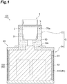
- FIG. 1 is a longitudinal cross-sectional view showing an X-ray generation device according to the embodiment.
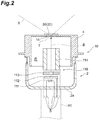
- FIG. 2 is a longitudinal cross-sectional view showing an X-ray tube according to the embodiment.
- an X-ray generation device 100 is, for example, a microfocus X-ray source used for X-ray nondestructive inspection for observing an internal structure of a test object.
- the X-ray generation device 100 is provided with an X-ray tube 1, a housing C, and a power supply portion 80.
- the X-ray tube 1 is a transmissive X-ray tube which emits an X-ray X from an X-ray emission window 30.
- the X-ray X is generated by an electron beam B from an electron gun 110 having entered a target T, and the target T transmits the X-ray X.
- the X-ray tube 1 is a vacuum sealed X-ray tube which is provided with a vacuum housing 10 including a vacuum internal space R and which does not require component replacement.
- the vacuum housing 10 has a substantially cylindrical outline.
- the vacuum housing 10 has a head unit 4 made of a metallic material (for example, stainless steel) and an insulating valve 2 made of an insulating material (for example, glass).
- the X-ray emission window 30 is fixed to the head unit 4.
- the electron gun 110 is fixed to the insulating valve 2.
- the insulating valve 2 has a cylindrical outline extending along the axis of the X-ray tube 1 and has a bottom 2a at an end opposite to the X-ray emission window 30.
- a stem pin S for power feeding or the like penetrates the bottom 2a and is held by the bottom 2a.
- the stem pin S holds the electron gun 110 at a predetermined position in the internal space R.
- the electron gun 110 includes a heater 111, a cathode 112 (electron-emitting unit), a first grid electrode 113 (electron quantity controlling electrode), and a second grid electrode 114.
- the heater 111 includes a filament that generates heat when energized.
- the cathode 112 functions as an electron-emitting source when heated by the heater 111.
- the first grid electrode 113 controls a quantity of electrons emitted from the cathode 112.
- the second grid electrode 114 having a cylindrical shape focuses electrons that have passed through the first grid electrode 113 toward the target T.
- the second grid electrode 114 doubles as an extraction electrode that forms an electric field for extracting electrons included in the electron beam B.
- the first grid electrode 113 is disposed between the cathode 112 and the second grid electrode 114.
- the X-ray tube 1 is fixed to one end of a cylindrical member 70 described below. Note that an exhaust pipe (not shown) is attached to the X-ray tube 1, and the inside of the X-ray tube 1 is evacuated through this exhaust pipe so as to be vacuum-sealed.
- the housing C of the X-ray generation device 100 includes the cylindrical member 70 and a power supply portion case 84 that houses an insulating block 81 which is to be described as a part of the power supply portion 80.
- the cylindrical member 70 is made of metal.
- the cylindrical member 70 has a cylindrical shape having openings at both ends.
- the insulating valve 2 of the X-ray tube 1 is inserted into an opening 70a at one end of the cylindrical member 70. Accordingly, the cylindrical member 70 houses at least a part of the X-ray tube 1.
- An attachment flange 3 of the X-ray tube 1 is brought into contact with one end surface of the cylindrical member 70 and is fixed thereto with a screw or the like. Accordingly, the X-ray tube 1 is fixed to the opening 70a of the cylindrical member 70 and seals the opening 70a.
- An insulating oil 71 which is a liquid electrical insulating substance is sealed within the cylindrical member 70.
- the power supply portion 80 has a function of supplying power to the X-ray tube 1.
- the power supply portion 80 includes the insulating block 81, a booster circuit (booster) 82, a control substrate (control unit) 83, and the power supply portion case 84.
- the insulating block 81 is made of a molded solid insulating material such as an epoxy resin which is an insulating resin.
- the booster circuit 82 is molded inside the insulating block 81.
- the control substrate 83 performs control to generate the X-ray X.
- the power supply portion case 84 having a rectangular box shape houses the insulating block 81, the booster circuit 82, and the control substrate 83.
- the booster circuit 82 generates a high voltage V.
- the insulating block 81 seals the booster circuit 82 with an insulating material (epoxy resin).
- the insulating block 81 is not limited to one that includes a single insulating material and may include a plurality of insulating materials (insulating resins) combined according to the desired insulating characteristics or elastic characteristics. Alternatively, the insulating block 81 may be one that is constituted by a plurality of molded bodies.
- the control substrate 83 performs the control to generate the X-ray X.
- the control substrate 83 controls voltages or currents supplied to the X-ray tube 1 or controls driving of the booster circuit 82 so as to control operations of the X-ray generation device 100.
- the control substrate 83 includes an internal substrate 83I molded inside the insulating block 81 and an external substrate 83E disposed outside the insulating block 81.
- the other end of the cylindrical member 70 (the opposite side of one end close to the X-ray tube 1) is fixed to the power supply portion 80. Accordingly, an opening 70b at the other end of the cylindrical member 70 is sealed, and the insulating oil 71 is airtightly sealed within the cylindrical member 70.
- a high-voltage power supply unit 90 is disposed on the insulating block 81.
- the high-voltage power supply unit 90 includes a cylindrical socket that is electrically connected to the booster circuit 82 and the control substrate 83.
- the power supply portion 80 is electrically connected to the X-ray tube 1 through the high-voltage power supply unit 90. More specifically, one end of the high-voltage power supply unit 90 close to the X-ray tube 1 is electrically connected to the stem pin S projecting from the bottom 2a of the insulating valve 2 in the X-ray tube 1. In addition, the other end of the high-voltage power supply unit 90 close to the power supply portion 80 is fixed to the insulating block 81 while electrically connected to the booster circuit 82 and the control substrate 83.
- the target T (anode) has a ground potential, and a negative high voltage (for example, from -10 kV to -500 kV) is supplied from the power supply portion 80 to the X-ray tube 1 (electron gun 110) via the high-voltage power supply unit 90.
- a negative high voltage for example, from -10 kV to -500 kV
- the X-ray tube 1 includes the vacuum housing 10 and a target unit 20.
- the side from which the X-ray tube 1 emits the X-ray X is simply referred to as "X-ray emission side" or "upper side".
- the X-ray emission side of the vacuum housing 10 is provided with the head unit 4 functioning as a wall portion that defines the internal space R.
- the head unit 4 is made of a metallic material (for example, stainless steel), and potentially corresponds to an anode of the X-ray tube 1.
- the head unit 4 has openings at both ends and has a substantially cylindrical shape coaxial with an axis of emission direction of the X-ray X. In an opening at the other end close to the electron gun 110, the head unit 4 communicates with the insulating valve 2 coaxial with the axis of emission direction (see FIG. 2 ).
- the target unit 20 is fixed to the head unit 4.
- the target unit 20 includes the X-ray emission window 30 and the target T.
- the X-ray emission window 30 is provided so as to seal an opening 14 of the vacuum housing 10 (head unit 4).
- the target T is provided on a side surface of the internal space R of the X-ray emission window 30.
- the target T generates the X-ray X by receiving the electron beam B.
- An example of the target T is made of tungsten.
- the X-ray emission window 30 has a disk shape.
- the X-ray emission window 30 is made of a material having high X-ray transmissivity such as beryllium and diamond.
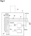
- FIG. 3 is a diagram showing the power supply portion of FIG. 1 .
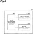
- FIG. 4 is a functional block diagram of the internal substrate of FIG. 3 .
- the power supply portion 80 includes the booster circuit 82.
- the booster circuit 82 includes a transformer 82t and a high-voltage generation circuit 82c.
- the high-voltage generation circuit 82c includes, for example, a multistage Cockcroft-Walton circuit.
- the booster circuit 82 boosts an input voltage Vo supplied via the external substrate 83E from an external power supply (not shown) connected to the X-ray generation device 100 so as to generate the high voltage V.
- the input voltage Vo has an absolute value of 100 V or less and is, for example, about -20 V in this embodiment.
- the power supply portion 80 includes the internal substrate 83I molded inside the insulating block 81 and the external substrate 83E disposed outside the insulating block 81.
- the internal substrate 83I includes a first internal substrate 83P and a second internal substrate 83Q arranged substantially parallel to each other.
- the first internal substrate 83P and the second internal substrate 83Q are disposed on both sides of a substrate base 89 which is made of a conductive material.
- the first internal substrate 83P and the second internal substrate 83Q are fixed together to the substrate base 89 and are electrically connected to each other through the substrate base 89.
- the first internal substrate 83P is disposed closer to the center of the insulating block 81 than the second internal substrate 83Q. Furthermore, the external substrate 83E is disposed outside the insulating block 81 and inside a space between the insulating block 81 and the power supply portion case 84.
- the control substrate 83 includes a control unit 95 that performs the control to generate the X-ray X.
- the control unit 95 includes at least a first information processing element 95a and a second information processing element 95b different from the first information processing element 95a.
- the first information processing element 95a and the second information processing element 95b are not a single electron device, such as a transistor and a resistor, which performs part of processing when forming a circuit.
- the first information processing element 95a and the second information processing element 95b are an integrated circuit element which includes a substrate on which various kinds of electron devices are mounted to make it into a circuit and which enables a series of information processing, that is, processing of a signal based on external input information, conversion of the signal into a signal indicating desired information, and output of the same.
- the first information processing element 95a and the second information processing element 95b include microcomputers and programmable logic devices (PLD) provided with a central processing unit (CPU) and a memory.
- PLD programmable logic devices
- the first information processing element 95a and the second information processing element 95b transmit and receive a digital signal and perform at least part of the control to generate the X-ray X using the digital signal.
- the control substrate 83 is provided with a control circuit that is driven based on the control by the first information processing element 95a and the second information processing element 95b.
- the control circuit outputs desired voltages or currents to, for example, the X-ray tube 1.
- the first information processing element 95a is mounted on a main surface 83s of the first internal substrate 83P that is on the opposite side of the substrate base 89. Accordingly, the first information processing element 95a is sealed with the insulating material (insulating resin) together with the booster circuit 82.
- the second information processing element 95b is mounted on the external substrate 83E. Accordingly the second information processing element 95b is disposed outside the insulating block 81 (exposed from the insulating material (insulating resin)).
- the external substrate 83E is a low-voltage operation substrate that operates at a low reference potential vp where a low potential based on a low voltage v lower than the high voltage V is regarded as a reference potential.
- the low voltage v may have an absolute value of 10 kV or less. More specifically, the absolute value is 1 kV or less. In this embodiment, the low voltage v is 0 V (ground potential).
- the external substrate 83E supplies the input voltage Vo from the outside to the high-voltage generation circuit 82c via the transformer 82t.
- the external substrate 83E is connected to the external power supply (not shown), and the input voltage Vo supplied from the external power supply to the external substrate 83E is primarily boosted to about several kV by the transformer 82t that electrically connects the external substrate 83E and the high-voltage generation circuit 82c, and then, the input voltage Vo is supplied to the high-voltage generation circuit 82c. Then, the high-voltage generation circuit 82c secondarily boosts the input voltage Vo and generates the high voltage V.
- the second information processing element 95b controls the external substrate 83E and the booster circuit 82.
- the second information processing element 95b controls the external substrate 83E, controls the supply of the input voltage Vo to the booster circuit 82, and controls the booster circuit 82, as the control to generate the X-ray X.
- the second information processing element 95b controls a high reference potential Vp where a high potential based on the high voltage V generated by the booster circuit 82 (high-voltage generation circuit 82c) is regarded as a reference potential. More specifically, the second information processing element 95b receives information associated with the actual value of the generated high voltage V from the booster circuit 82 or the like, and then, feedbacks the high voltage V (high reference potential Vp) based on the information. Note that a current is also supplied from the external power supply, and the current is controlled by the second information processing element 95b in a similar manner to the voltage. In other words, the second information processing element 95b controls the power supplied from the external power supply to the booster circuit 82.
- the internal substrate 83I is electrically connected to the booster circuit 82 (high-voltage generation circuit 82c) via a current-limiting resistor 85. More specifically, the internal substrate 83I is electrically connected to the booster circuit 82 (high-voltage generation circuit 82c) through the current-limiting resistor 85, a cover electrode 88 to be described, and the substrate base 89. Accordingly, the high voltage V from the booster circuit 82 (high-voltage generation circuit 82c) is applied to the internal substrate 83I (the first internal substrate 83P and the second internal substrate 83Q).
- the internal substrate 83I (the first internal substrate 83P and the second internal substrate 83Q) is a high-voltage operation substrate that operates at the high reference potential Vp where the high potential based on the high voltage V is regarded as a reference potential.
- the first information processing element 95a also operates at the high reference potential Vp where the high potential based on the high voltage V is regarded as a reference potential.
- the high voltage V (high reference potential Vp) is, for example, -100 kV. While the high voltage V is insulated, a drive power E for driving the first internal substrate 83P, the second internal substrate 83Q, and the first information processing element 95a included in the internal substrate 83I is supplied from the external substrate 83E to the internal substrate 83I through the transformer 86 molded inside the insulating block 81.
- the first internal substrate 83P, the second internal substrate 83Q, and the first information processing element 95a included in the internal substrate 83I are driven by the drive power E while the high reference potential Vp is regarded as an imaginary ground potential.
- the first information processing element 95a electrically connects the heater 111, the cathode 112, the first grid electrode 113, and the second grid electrode 114 which are included in the electron gun 110 via the high-voltage power supply unit 90 and the stem pin S. Accordingly, the first information processing element 95a at least partially controls driving of components such as the heater 111, the cathode 112, the first grid electrode 113, and the second grid electrode 114 (the electron gun 110) which are relevant to the generation of the X-ray X in the X-ray tube 1.
- the first information processing element 95a controls the power supplied to each of those components.
- the first information processing element 95a controls the first grid electrode 113 to have a voltage about -1500 V
- the cathode 112 controls a voltage about -1000 V
- the heater 111 controls a voltage about -5 V from the potential of the cathode 112
- the second grid electrode 114 to have a voltage of 0 V (that is, an imaginary ground potential).
- the first information processing element 95a controls an actual applied voltage with respect to the first grid electrode 113, the cathode 112, the heater 111, and the second grid electrode 114 to be, for example, -100 kV + (-1500 V), -100 kV + (-1000 V), -100 kV + (-1000 V) + (-5 V), and -100 kV, respectively.
- the second grid electrode 114 may be electrically connected to the booster circuit 82 (high-voltage generation circuit 82c) in a direct manner without the internal substrate 83I (first information processing element 95a) involved.
- the second grid electrode 114 is controlled by the second information processing element 95b of the external substrate 83E in a similar manner to the booster circuit 82.
- the first information processing element 95a performs feedback control on a tube current by controlling the heater 111, the cathode 112, and the first grid electrode 113 and performs feedback control on focus (focus of the electron beam B) by controlling the cathode 112 and the second grid electrode 114.
- a voltage Vr in a predetermined range from -1500 V to 0 V is added to the high voltage V (-100 kV) which is at the high reference potential Vp, and the voltage Vr is appropriately applied to each of the heater 111, the cathode 112, the first grid electrode 113, and the second grid electrode 114.
- the high voltage V is attributed to a voltage supplied from the booster circuit 82
- the voltage Vr in the predetermined range is attributed to a driving power supply (not shown) provided in the internal substrate 83I and driven by the drive power W.
- the voltage Vr in the predetermined range is 0 V (that is, when the voltage Vr is equal to the high voltage V)
- the voltage Vr may be supplied from the booster circuit 82 without using the driving power supply.
- the first information processing element 95a controls the electron gun 110 at the voltage Vr in the predetermined range while the high reference potential Vp is regarded as an imaginary ground potential.
- the above voltages are an example, and the voltages applied to the components of the electron gun 110 (the heater 111, the cathode 112, the first grid electrode 113, and the second grid electrode 114) may be changed appropriately.
- the high voltage V and the voltage Vr in the predetermined range may be defined in the following manner. That is, the absolute value of the high voltage V (high reference potential Vp) controlled by the first information processing element 95a may be 10 kV or more and 500 kV or less.
- the voltage Vr in the predetermined range excluding a voltage corresponding to the high voltage V may be 4% or less of the high voltage V
- the maximum of the absolute value of the voltage Vr in the predetermined range may be 25 V or more and 20 kV or less.
- the absolute value of the high voltage V (high reference potential Vp) is 10 kV or more and 300 kV or less
- the voltage Vr in the predetermined range is 2% or less of the high voltage V
- the maximum of the absolute value of the voltage Vr in the predetermined range is 50 V or more and 6 kV or less.
- the voltage Vr in the predetermined range includes a voltage at 0% of the high voltage V
- the voltage Vr also includes a case where a voltage applied to each component of the electron gun 110 in the X-ray tube 1 (that is, the heater 111, the cathode 112, the first grid electrode 113, and the second grid electrode 114) controlled by the first information processing element 95a is equal to the high voltage V generated by the booster circuit 82 (high-voltage generation circuit 82c).
- the electron gun 110 includes the heater 111 including a filament that generates heat when energized; the cathode 112 that functions as an electron-emitting source when heated by the heater 111; the second grid electrode 114 as an extraction electrode that forms an electric field for extracting electrons included in the electron beam B from the cathode 112; and the first grid electrode 113 which is disposed between the cathode 112 and the second grid electrode 114 and which controls a quantity of electrons emitted from the cathode 112.
- the first information processing element 95a controls applied voltages to drive at least a part of components (the electron gun 110), for example, the heater 111, the cathode 112, the first grid electrode 113, and the second grid electrode 114 which are relevant to the generation of the X-ray X in the X-ray tube 1.
- the first information processing element 95a controls the tube current in the X-ray tube 1 and controls the focus.
- the internal substrate 83I includes the first information processing element 95a (for example, a microcomputer or PLD), a tube-current control circuit 95d driven by the control of the first information processing element 95a, and a focus control circuit 95e. At least a part of the driving power supply that supplies the voltage Vr in the predetermined range is included in the tube-current control circuit 95d and the focus control circuit 95e.
- the first information processing element 95a transmits and receives a digital signal that indicate control information between the second information processing element 95b (for example, a microcomputer or PLD) that stores data of various kinds of supply electrodes based on predetermined drive conditions in the X-ray tube 1.
- the second information processing element 95b for example, a microcomputer or PLD
- the communication unit used to transmit and receive a digital signal may be wireless or the like.
- Digital signals are excellent in processing ability and noise resistance with respect to minute signals, which enables transmission and reception of high-accuracy signals. Accordingly, it is possible to control outputs to the tube-current control circuit 95d and the focus control circuit 95e with high accuracy, that is, within the error range of 0.1% or less, even between the internal substrate 83I and the external substrate 83E, or between the high reference potential Vp and the low reference potential vp, which greatly differ to each other in potential.
- the transmission and reception of signals between the first information processing element 95a and the second information processing element 95b are not limited to digital signals, and FM communication or the like may be employed.
- the second information processing element 95b when a signal indicating control information is input to the second information processing element 95b from an external input unit (not shown) such as a personal computer connected to the X-ray generation device 100, based on the signal, the second information processing element 95b outputs a digital signal indicating the control information to the first information processing element 95a, and the first information processing element 95a performs information processing using the digital signal.
- the first information processing element 95a When the tube current is to be controlled, the first information processing element 95a outputs a signal to the tube-current control circuit 95d.
- the tube-current control circuit 95d supplies a drive voltage to the heater 111, the cathode 112, and the first grid electrode 113 using the high voltage V and the voltage Vr in the predetermined range according to the input signal.
- the first information processing element 95a controls the tube current in the X-ray tube 1. Furthermore, when tube current information is input from a tube current acquisition unit (not shown) to the first information processing element 95a, the first information processing element 95a performs feedback control of the tube current.
- the first information processing element 95a When the focus is to be controlled, the first information processing element 95a outputs a signal to the focus control circuit 95e.
- the focus control circuit 95e supplies a drive voltage to the cathode 112 and the second grid electrode 114 using the high voltage V and the voltage Vr in the predetermined range according to the input signal. Accordingly, the first information processing element 95a controls the focus in the X-ray tube 1. Furthermore, when focus information is input from a focus information acquisition unit (not shown) to the first information processing element 95a, the first information processing element 95a performs feedback control of the focus.
- the power supply portion 80 further includes the cover electrode (conductive member) 88.
- the cover electrode 88 is made of, for example, a metallic material such as stainless steel or aluminum.
- the cover electrode 88 is sealed with the insulating material (insulating resin) in the insulating block 81.
- the cover electrode 88 is formed into an L-shape by a first portion 88a and a second portion 88b both having a flat-plate shape.
- the first portion 88a extends along the central axis of the X-ray generation device 100.
- the second portion 88b is erected in a direction intersecting with an extension direction of the first portion 88a at an upper end of the first portion 88a (an end close to the X-ray tube 1) in a direction along the central axis of the X-ray generation device 100.
- the cover electrode 88 is disposed such that the first portion 88a faces the main surface 83s of the first internal substrate 83P. Accordingly, when viewed in a direction intersecting the main surface 83s, most of the main surface 83s and the entire first information processing element 95a on the main surface 83s are covered with the cover electrode 88 (first portion 88a). In other words, the cover electrode 88 (first portion 88a) blocks the booster circuit 82 (high-voltage generation circuit 82c) from the first information processing element 95a (main surface 83s of the first internal substrate 83P).
- the power supply portion 80 includes the cover electrode 88 which covers at least a part of the first information processing element 95a and which is sealed with the insulating material (insulating resin) in the insulating block 81.
- a voltage Vc based on the high voltage V is applied to the cover electrode 88.
- the voltage Vc is, for example, obtained by adding the voltage Vr in the predetermined range to the high voltage V.
- the voltage Vc is equal to the high voltage V since the voltage Vc is supplied from the booster circuit 82 (high-voltage generation circuit 82c) via the current-limiting resistor 85.
- the high voltage V is applied to the substrate base 89, the first internal substrate 83P, and the second internal substrate 83Q.
- the first internal substrate 83P and the second internal substrate 83Q are fixed, and the substrate base 89 electrically connected to those internal substrates is electrically connected to the cover electrode 88.
- the first information processing element 95a that operates at the high reference potential Vp is surrounded by the cover electrode 88 and the substrate base 89 which also operate at the high reference potential Vp (high voltage V)
- an electric field around the first information processing element 95a is stabilized, which enables stable operation of the first information processing element 95a.
- the X-ray generation device 100 includes the X-ray tube 1 and the power supply portion 80.
- the power supply portion 80 supplies the high voltage V to the X-ray tube 1.
- the power supply portion 80 includes the booster circuit 82 that boosts the input voltage Vo from the outside to generate the high voltage V. Since the booster circuit 82 is a high-voltage section, the insulating block 81 is sealed with the insulating material (insulating resin).
- the power supply portion 80 includes the control unit 95 that performs the control to generate the X-ray X.
- the control unit 95 includes the first information processing element 95a that performs at least part of the control to generate the X-ray X using a digital signal.
- the first information processing element 95a is sealed with the insulating material (insulating resin) in the insulating block 81 together with the booster circuit 82. Accordingly, even at the high reference potential Vp based on the high voltage V, the first information processing element 95a enables stable control.
- the power supply portion 80 further includes the cover electrode 88 which covers at least a part of the first information processing element 95a and which is sealed with the insulating material (insulating resin) in the insulating block 81.
- the voltage Vc based on the high voltage V is applied to the cover electrode 88. Therefore, an electric field around the first information processing element 95a is stabilized, which enables stable operation of the first information processing element 95a.
- the potentials of the X-ray tube 1 and the internal substrate 83I quickly drop to the ground potential through a discharging path generated in the X-ray tube 1.
- the potential of the booster circuit 82 (high-voltage generation circuit 82c) drops to the ground potential in the discharging path after passing through the current-limiting resistor 85 or drops to the ground potential through the multistage Cockcroft-Walton circuit.
- the internal substrate 83I (the first internal substrate 83P, the second internal substrate 83Q, and the first information processing element 95a) reaches the ground potential first, and then, the booster circuit 82 (high-voltage generation circuit 82c) reaches the ground potential with a slight difference in time. Therefore, in a short time, a potential difference corresponding to the high voltage V (high reference potential Vp) at a maximum is generated between the first information processing element 95a and the booster circuit 82 (high-voltage generation circuit 82c), which may cause a very strong electric field. Therefore, if the electric field reaches the first information processing element 95a, the first information processing element 95a may be broken.
- the cover electrode 88 (first portion 88a) blocks the booster circuit 82 (high-voltage generation circuit 82c) from the first information processing element 95a. Accordingly, for example, even when a discharge occurs in the X-ray tube 1 as described above, the cover electrode 88 prevents influences of an electric field generated by the discharge, which prevents failure of the first information processing element 95a. Furthermore, the first information processing element 95a includes the second portion 88b that blocks the first information processing element 95a from the X-ray tube 1, and the second portion 88b prevents the first information processing element 95a from being directly affected by the discharge in the X-ray tube 1.
- the first information processing element 95a controls the electron gun 110 at the high reference potential Vp. As described above, herein, the first information processing element 95a is sealed with the insulating material (insulating resin) in the insulating block 81. Accordingly, it is possible to stably control the generation and emission of the electron beam from the electron gun 110.
- the control unit 95 further includes the second (another) information processing element 95b that performs the control to generate the X-ray X at the low reference potential vp based on the low voltage v lower than the high voltage V.
- the second information processing element 95b is disposed outside the insulating block 81. Accordingly, the second information processing element 95b disposed outside the insulating block 81 makes it possible to stably control generation of the X-ray X.
- the aforementioned embodiment illustrates an embodiment of the X-ray generation device according to an aspect of the present invention. Therefore, the X-ray generation device according to an aspect of the present invention is not limited to the X-ray generation device 100.
- the X-ray generation device according to an aspect of the present invention may be one obtained by optionally modifying the X-ray generation device 100 within the scope of the claims.
- the insulating material forming the insulating block 81 is not limited to an insulating resin and may be an insulating material other than the resin, for example, ceramic.
- the high voltage V may be supplied not to the electron gun 110 but to the target T.
- the X-ray tube may not necessarily be of the transmissive type but may be of a reflective type in which a reflective target is used.
- the electron gun 110 may include another grid electrode or may use a cold cathode.
- an X-ray generation device that enables stable control at a high potential.
Landscapes
- Health & Medical Sciences (AREA)
- General Health & Medical Sciences (AREA)
- Toxicology (AREA)
- X-Ray Techniques (AREA)
Abstract
Description
- An aspect of the present invention relates to an X-ray generation device.
-
Patent Literature 1 discloses an industrial X-ray generation device. The device is provided with an X-ray tube mounted on a base and having a cylindrical tubular body. The inside of the tubular body is provided with a cathode that emits electrons, a grid or an extraction electrode, and an anode that attracts electrons. The anode has targets with which electrons collide to generate X-rays. Furthermore, in this device, a high-voltage power supply portion including a booster circuit and a controller is provided on the base. The controller includes a microcomputer provided with, for example, a central processing unit (CPU) and a memory. The X-ray tube and the booster circuit are subjected to molding and covered with a molding material. - Patent Literature 1: Japanese Patent No.
5780644 - In the aforementioned device, the controller is housed in an outer case. Accordingly, when the controller is operated at a high potential, the controller is heavily impacted by a discharge inside the device. Particularly, an information processing element, such as a microcomputer included in a controller, which performs information processing based on digital signals may be seriously damaged because such an element is designed on the premise of operating at a low potential and is weak against a discharge at a high potential where a potential difference becomes large. For that reason, it is difficult to perform stable control at a high potential.
- An aspect of the present invention aims to provide an X-ray generation device that enables stable control at a high potential.
- An X-ray generation device according to an aspect of the present invention includes an X-ray tube including an electron gun configured to generate an electron beam and a target configured to generate an X-ray by incidence of the electron beam; a power supply portion including a booster configured to boost an input voltage from outside to generate a high voltage and an insulating block configured to seal the booster with an insulating material; and a control unit configured to perform control to generate the X-ray, wherein the control unit includes a first information processing element configured to perform at least part of the control using a digital signal at a high potential based on the high voltage, wherein the first information processing element is sealed with the insulating material in the insulating block.
- The X-ray generation device is provided with the X-ray tube, the power supply portion, and the control unit. The power supply portion includes the booster that boosts an input voltage from outside to generate a high voltage. The booster is sealed with the insulating material in the insulating block. The control unit that performs the control to generate the X-ray includes the first information processing element that performs at least part of the control to generate the X-ray using a digital signal at a high potential based on the high voltage. The first information processing element is sealed with the insulating material in the insulating block. Accordingly, the first information processing element enables stable control even at a high potential.
- In the X-ray generation device according to an aspect of the present invention, the power supply portion may further include a conductive member which covers at least a part of the first information processing element and which is sealed with the insulating material in the insulating block, and a voltage based on the high voltage may be applied to the conductive member. In this case, an electric field around the first information processing element is stabilized, which enables stable operation of the first information processing element.
- In the X-ray generation device according to an aspect of the present invention, the first information processing element may control the electron gun at a high potential. In this case, it is possible to stably control the generation and emission of the electron beam from the electron gun.
- In the X-ray generation device according to an aspect of the present invention, the control unit may further include a second information processing element that performs the control at a low potential based on a low voltage lower than the high voltage, and the second information processing element may be disposed outside the insulating block. In this case, the generation and emission of the electron beam is stably controlled by the second information processing element disposed outside the insulating block.
- According to an aspect of the present invention, there is provided an X-ray generation device that enables stable control at a high potential.
-
-
FIG. 1 is a longitudinal cross-sectional view showing an X-ray generation device according to an embodiment. -
FIG. 2 is a longitudinal cross-sectional view showing an X-ray tube according to an embodiment. -
FIG. 3 is a view showing a power supply portion shown inFIG. 1 . -
FIG. 4 is a functional block diagram of an internal substrate shown inFIG. 3 . - An embodiment according to an aspect of the present invention will now be described in detail with reference to the accompanying drawings. In each drawing, the same or corresponding elements are denoted by the same reference numerals, and redundant description may be omitted.
-
FIG. 1 is a longitudinal cross-sectional view showing an X-ray generation device according to the embodiment.FIG. 2 is a longitudinal cross-sectional view showing an X-ray tube according to the embodiment. As shown inFIGS. 1 and2 , anX-ray generation device 100 is, for example, a microfocus X-ray source used for X-ray nondestructive inspection for observing an internal structure of a test object. TheX-ray generation device 100 is provided with anX-ray tube 1, a housing C, and apower supply portion 80. - The
X-ray tube 1 is a transmissive X-ray tube which emits an X-ray X from anX-ray emission window 30. The X-ray X is generated by an electron beam B from anelectron gun 110 having entered a target T, and the target T transmits the X-ray X. TheX-ray tube 1 is a vacuum sealed X-ray tube which is provided with avacuum housing 10 including a vacuum internal space R and which does not require component replacement. - The
vacuum housing 10 has a substantially cylindrical outline. Thevacuum housing 10 has ahead unit 4 made of a metallic material (for example, stainless steel) and an insulatingvalve 2 made of an insulating material (for example, glass). TheX-ray emission window 30 is fixed to thehead unit 4. Theelectron gun 110 is fixed to the insulatingvalve 2. Theinsulating valve 2 has a cylindrical outline extending along the axis of theX-ray tube 1 and has abottom 2a at an end opposite to theX-ray emission window 30. A stem pin S for power feeding or the like penetrates thebottom 2a and is held by thebottom 2a. The stem pin S holds theelectron gun 110 at a predetermined position in the internal space R. - The
electron gun 110 includes aheater 111, a cathode 112 (electron-emitting unit), a first grid electrode 113 (electron quantity controlling electrode), and asecond grid electrode 114. Theheater 111 includes a filament that generates heat when energized. Thecathode 112 functions as an electron-emitting source when heated by theheater 111. Thefirst grid electrode 113 controls a quantity of electrons emitted from thecathode 112. Thesecond grid electrode 114 having a cylindrical shape focuses electrons that have passed through thefirst grid electrode 113 toward the target T. Thesecond grid electrode 114 doubles as an extraction electrode that forms an electric field for extracting electrons included in the electron beam B. Thefirst grid electrode 113 is disposed between thecathode 112 and thesecond grid electrode 114. TheX-ray tube 1 is fixed to one end of acylindrical member 70 described below. Note that an exhaust pipe (not shown) is attached to theX-ray tube 1, and the inside of theX-ray tube 1 is evacuated through this exhaust pipe so as to be vacuum-sealed. - The housing C of the
X-ray generation device 100 includes thecylindrical member 70 and a powersupply portion case 84 that houses an insulatingblock 81 which is to be described as a part of thepower supply portion 80. Thecylindrical member 70 is made of metal. Thecylindrical member 70 has a cylindrical shape having openings at both ends. The insulatingvalve 2 of theX-ray tube 1 is inserted into anopening 70a at one end of thecylindrical member 70. Accordingly, thecylindrical member 70 houses at least a part of theX-ray tube 1. - An
attachment flange 3 of theX-ray tube 1 is brought into contact with one end surface of thecylindrical member 70 and is fixed thereto with a screw or the like. Accordingly, theX-ray tube 1 is fixed to theopening 70a of thecylindrical member 70 and seals theopening 70a. An insulatingoil 71 which is a liquid electrical insulating substance is sealed within thecylindrical member 70. - The
power supply portion 80 has a function of supplying power to theX-ray tube 1. Thepower supply portion 80 includes the insulatingblock 81, a booster circuit (booster) 82, a control substrate (control unit) 83, and the powersupply portion case 84. The insulatingblock 81 is made of a molded solid insulating material such as an epoxy resin which is an insulating resin. Thebooster circuit 82 is molded inside the insulatingblock 81. Thecontrol substrate 83 performs control to generate the X-ray X. The powersupply portion case 84 having a rectangular box shape houses the insulatingblock 81, thebooster circuit 82, and thecontrol substrate 83. Thebooster circuit 82 generates a high voltage V. The insulatingblock 81 seals thebooster circuit 82 with an insulating material (epoxy resin). The insulatingblock 81 is not limited to one that includes a single insulating material and may include a plurality of insulating materials (insulating resins) combined according to the desired insulating characteristics or elastic characteristics. Alternatively, the insulatingblock 81 may be one that is constituted by a plurality of molded bodies. - The
control substrate 83 performs the control to generate the X-ray X. For example, thecontrol substrate 83 controls voltages or currents supplied to theX-ray tube 1 or controls driving of thebooster circuit 82 so as to control operations of theX-ray generation device 100. Thecontrol substrate 83 includes an internal substrate 83I molded inside the insulatingblock 81 and anexternal substrate 83E disposed outside the insulatingblock 81. The other end of the cylindrical member 70 (the opposite side of one end close to the X-ray tube 1) is fixed to thepower supply portion 80. Accordingly, anopening 70b at the other end of thecylindrical member 70 is sealed, and the insulatingoil 71 is airtightly sealed within thecylindrical member 70. - A high-voltage
power supply unit 90 is disposed on the insulatingblock 81. The high-voltagepower supply unit 90 includes a cylindrical socket that is electrically connected to thebooster circuit 82 and thecontrol substrate 83. Thepower supply portion 80 is electrically connected to theX-ray tube 1 through the high-voltagepower supply unit 90. More specifically, one end of the high-voltagepower supply unit 90 close to theX-ray tube 1 is electrically connected to the stem pin S projecting from the bottom 2a of the insulatingvalve 2 in theX-ray tube 1. In addition, the other end of the high-voltagepower supply unit 90 close to thepower supply portion 80 is fixed to the insulatingblock 81 while electrically connected to thebooster circuit 82 and thecontrol substrate 83. - In this embodiment, the target T (anode) has a ground potential, and a negative high voltage (for example, from -10 kV to -500 kV) is supplied from the
power supply portion 80 to the X-ray tube 1 (electron gun 110) via the high-voltagepower supply unit 90. - The
X-ray tube 1 includes thevacuum housing 10 and atarget unit 20. In this embodiment, the side from which theX-ray tube 1 emits the X-ray X is simply referred to as "X-ray emission side" or "upper side". The X-ray emission side of thevacuum housing 10 is provided with thehead unit 4 functioning as a wall portion that defines the internal space R. Thehead unit 4 is made of a metallic material (for example, stainless steel), and potentially corresponds to an anode of theX-ray tube 1. Thehead unit 4 has openings at both ends and has a substantially cylindrical shape coaxial with an axis of emission direction of the X-ray X. In an opening at the other end close to theelectron gun 110, thehead unit 4 communicates with the insulatingvalve 2 coaxial with the axis of emission direction (seeFIG. 2 ). - The
target unit 20 is fixed to thehead unit 4. Thetarget unit 20 includes theX-ray emission window 30 and the target T. TheX-ray emission window 30 is provided so as to seal anopening 14 of the vacuum housing 10 (head unit 4). The target T is provided on a side surface of the internal space R of theX-ray emission window 30. The target T generates the X-ray X by receiving the electron beam B. An example of the target T is made of tungsten. TheX-ray emission window 30 has a disk shape. TheX-ray emission window 30 is made of a material having high X-ray transmissivity such as beryllium and diamond. - Next, the
power supply portion 80 will be specifically described with further reference toFIGS. 3 and4 .FIG. 3 is a diagram showing the power supply portion ofFIG. 1 .FIG. 4 is a functional block diagram of the internal substrate ofFIG. 3 . Thepower supply portion 80 includes thebooster circuit 82. Thebooster circuit 82 includes atransformer 82t and a high-voltage generation circuit 82c. The high-voltage generation circuit 82c includes, for example, a multistage Cockcroft-Walton circuit. Thebooster circuit 82 boosts an input voltage Vo supplied via theexternal substrate 83E from an external power supply (not shown) connected to theX-ray generation device 100 so as to generate the high voltage V. The input voltage Vo has an absolute value of 100 V or less and is, for example, about -20 V in this embodiment. - As the
control substrate 83 that performs the control to generate the X-ray X, thepower supply portion 80 includes the internal substrate 83I molded inside the insulatingblock 81 and theexternal substrate 83E disposed outside the insulatingblock 81. The internal substrate 83I includes a firstinternal substrate 83P and a secondinternal substrate 83Q arranged substantially parallel to each other. The firstinternal substrate 83P and the secondinternal substrate 83Q are disposed on both sides of asubstrate base 89 which is made of a conductive material. The firstinternal substrate 83P and the secondinternal substrate 83Q are fixed together to thesubstrate base 89 and are electrically connected to each other through thesubstrate base 89. Herein, the firstinternal substrate 83P is disposed closer to the center of the insulatingblock 81 than the secondinternal substrate 83Q. Furthermore, theexternal substrate 83E is disposed outside the insulatingblock 81 and inside a space between the insulatingblock 81 and the powersupply portion case 84. - The
control substrate 83 includes acontrol unit 95 that performs the control to generate the X-ray X. Thecontrol unit 95 includes at least a firstinformation processing element 95a and a secondinformation processing element 95b different from the firstinformation processing element 95a. The firstinformation processing element 95a and the secondinformation processing element 95b are not a single electron device, such as a transistor and a resistor, which performs part of processing when forming a circuit. The firstinformation processing element 95a and the secondinformation processing element 95b are an integrated circuit element which includes a substrate on which various kinds of electron devices are mounted to make it into a circuit and which enables a series of information processing, that is, processing of a signal based on external input information, conversion of the signal into a signal indicating desired information, and output of the same. Specifically, examples of the firstinformation processing element 95a and the secondinformation processing element 95b include microcomputers and programmable logic devices (PLD) provided with a central processing unit (CPU) and a memory. The firstinformation processing element 95a and the secondinformation processing element 95b transmit and receive a digital signal and perform at least part of the control to generate the X-ray X using the digital signal. In addition, thecontrol substrate 83 is provided with a control circuit that is driven based on the control by the firstinformation processing element 95a and the secondinformation processing element 95b. The control circuit outputs desired voltages or currents to, for example, theX-ray tube 1. - The first
information processing element 95a is mounted on amain surface 83s of the firstinternal substrate 83P that is on the opposite side of thesubstrate base 89. Accordingly, the firstinformation processing element 95a is sealed with the insulating material (insulating resin) together with thebooster circuit 82. On the other hand, the secondinformation processing element 95b is mounted on theexternal substrate 83E. Accordingly the secondinformation processing element 95b is disposed outside the insulating block 81 (exposed from the insulating material (insulating resin)). - The
external substrate 83E is a low-voltage operation substrate that operates at a low reference potential vp where a low potential based on a low voltage v lower than the high voltage V is regarded as a reference potential. In other words, since theexternal substrate 83E operates under an environment that is potentially extremely stable, theexternal substrate 83E is used for comprehensive control of the entireX-ray generation device 100. The low voltage v may have an absolute value of 10 kV or less. More specifically, the absolute value is 1 kV or less. In this embodiment, the low voltage v is 0 V (ground potential). Theexternal substrate 83E supplies the input voltage Vo from the outside to the high-voltage generation circuit 82c via thetransformer 82t. - More specifically, the
external substrate 83E is connected to the external power supply (not shown), and the input voltage Vo supplied from the external power supply to theexternal substrate 83E is primarily boosted to about several kV by thetransformer 82t that electrically connects theexternal substrate 83E and the high-voltage generation circuit 82c, and then, the input voltage Vo is supplied to the high-voltage generation circuit 82c. Then, the high-voltage generation circuit 82c secondarily boosts the input voltage Vo and generates the high voltage V. The secondinformation processing element 95b controls theexternal substrate 83E and thebooster circuit 82. In other words, at the low reference potential vp, or at the low potential based on the low voltage v, the secondinformation processing element 95b controls theexternal substrate 83E, controls the supply of the input voltage Vo to thebooster circuit 82, and controls thebooster circuit 82, as the control to generate the X-ray X. - In short, the second
information processing element 95b controls a high reference potential Vp where a high potential based on the high voltage V generated by the booster circuit 82 (high-voltage generation circuit 82c) is regarded as a reference potential. More specifically, the secondinformation processing element 95b receives information associated with the actual value of the generated high voltage V from thebooster circuit 82 or the like, and then, feedbacks the high voltage V (high reference potential Vp) based on the information. Note that a current is also supplied from the external power supply, and the current is controlled by the secondinformation processing element 95b in a similar manner to the voltage. In other words, the secondinformation processing element 95b controls the power supplied from the external power supply to thebooster circuit 82. - The internal substrate 83I is electrically connected to the booster circuit 82 (high-
voltage generation circuit 82c) via a current-limitingresistor 85. More specifically, the internal substrate 83I is electrically connected to the booster circuit 82 (high-voltage generation circuit 82c) through the current-limitingresistor 85, acover electrode 88 to be described, and thesubstrate base 89. Accordingly, the high voltage V from the booster circuit 82 (high-voltage generation circuit 82c) is applied to the internal substrate 83I (the firstinternal substrate 83P and the secondinternal substrate 83Q). In other words, the internal substrate 83I (the firstinternal substrate 83P and the secondinternal substrate 83Q) is a high-voltage operation substrate that operates at the high reference potential Vp where the high potential based on the high voltage V is regarded as a reference potential. - Accordingly, the first
information processing element 95a also operates at the high reference potential Vp where the high potential based on the high voltage V is regarded as a reference potential. The high voltage V (high reference potential Vp) is, for example, -100 kV. While the high voltage V is insulated, a drive power E for driving the firstinternal substrate 83P, the secondinternal substrate 83Q, and the firstinformation processing element 95a included in the internal substrate 83I is supplied from theexternal substrate 83E to the internal substrate 83I through thetransformer 86 molded inside the insulatingblock 81. In other words, the firstinternal substrate 83P, the secondinternal substrate 83Q, and the firstinformation processing element 95a included in the internal substrate 83I are driven by the drive power E while the high reference potential Vp is regarded as an imaginary ground potential. - In addition, the first
information processing element 95a electrically connects theheater 111, thecathode 112, thefirst grid electrode 113, and thesecond grid electrode 114 which are included in theelectron gun 110 via the high-voltagepower supply unit 90 and the stem pin S. Accordingly, the firstinformation processing element 95a at least partially controls driving of components such as theheater 111, thecathode 112, thefirst grid electrode 113, and the second grid electrode 114 (the electron gun 110) which are relevant to the generation of the X-ray X in theX-ray tube 1. - Specifically, the first
information processing element 95a controls the power supplied to each of those components. Herein, an example of the control of an applied voltage to each component will be described. At the high reference potential Vp based on the high voltage V of -100 kV, the firstinformation processing element 95a controls thefirst grid electrode 113 to have a voltage about -1500 V, thecathode 112 to have a voltage about -1000 V, theheater 111 to have a voltage about -5 V from the potential of thecathode 112, and thesecond grid electrode 114 to have a voltage of 0 V (that is, an imaginary ground potential). In other words, the firstinformation processing element 95a controls an actual applied voltage with respect to thefirst grid electrode 113, thecathode 112, theheater 111, and thesecond grid electrode 114 to be, for example, -100 kV + (-1500 V), -100 kV + (-1000 V), -100 kV + (-1000 V) + (-5 V), and -100 kV, respectively. - As in the above example, when a voltage equal to the high voltage V which is at the high reference potential Vp is supplied to the
second grid electrode 114, thesecond grid electrode 114 may be electrically connected to the booster circuit 82 (high-voltage generation circuit 82c) in a direct manner without the internal substrate 83I (firstinformation processing element 95a) involved. In this case, thesecond grid electrode 114 is controlled by the secondinformation processing element 95b of theexternal substrate 83E in a similar manner to thebooster circuit 82. Furthermore, the firstinformation processing element 95a performs feedback control on a tube current by controlling theheater 111, thecathode 112, and thefirst grid electrode 113 and performs feedback control on focus (focus of the electron beam B) by controlling thecathode 112 and thesecond grid electrode 114. - In the above example, a voltage Vr in a predetermined range from -1500 V to 0 V is added to the high voltage V (-100 kV) which is at the high reference potential Vp, and the voltage Vr is appropriately applied to each of the
heater 111, thecathode 112, thefirst grid electrode 113, and thesecond grid electrode 114. However, note that the high voltage V is attributed to a voltage supplied from thebooster circuit 82, while the voltage Vr in the predetermined range is attributed to a driving power supply (not shown) provided in the internal substrate 83I and driven by the drive power W. When the voltage Vr in the predetermined range is 0 V (that is, when the voltage Vr is equal to the high voltage V), the voltage Vr may be supplied from thebooster circuit 82 without using the driving power supply. In other words, the firstinformation processing element 95a controls theelectron gun 110 at the voltage Vr in the predetermined range while the high reference potential Vp is regarded as an imaginary ground potential. - However, the above voltages are an example, and the voltages applied to the components of the electron gun 110 (the
heater 111, thecathode 112, thefirst grid electrode 113, and the second grid electrode 114) may be changed appropriately. Furthermore, the high voltage V and the voltage Vr in the predetermined range may be defined in the following manner. That is, the absolute value of the high voltage V (high reference potential Vp) controlled by the firstinformation processing element 95a may be 10 kV or more and 500 kV or less. In this case, in the voltages applied to the components of theelectron gun 110 in the X-ray tube 1 (theheater 111, thecathode 112, thefirst grid electrode 113, and the second grid electrode 114) controlled by the firstinformation processing element 95a, the voltage Vr in the predetermined range excluding a voltage corresponding to the high voltage V (that is, a voltage corresponding to a potential difference with respect to the high reference potential Vp) may be 4% or less of the high voltage V, and the maximum of the absolute value of the voltage Vr in the predetermined range may be 25 V or more and 20 kV or less. More specifically, the absolute value of the high voltage V (high reference potential Vp) is 10 kV or more and 300 kV or less, the voltage Vr in the predetermined range is 2% or less of the high voltage V, and the maximum of the absolute value of the voltage Vr in the predetermined range is 50 V or more and 6 kV or less. Since the voltage Vr in the predetermined range includes a voltage at 0% of the high voltage V, the voltage Vr also includes a case where a voltage applied to each component of theelectron gun 110 in the X-ray tube 1 (that is, theheater 111, thecathode 112, thefirst grid electrode 113, and the second grid electrode 114) controlled by the firstinformation processing element 95a is equal to the high voltage V generated by the booster circuit 82 (high-voltage generation circuit 82c). - As described above, in the
X-ray generation device 100, theelectron gun 110 includes theheater 111 including a filament that generates heat when energized; thecathode 112 that functions as an electron-emitting source when heated by theheater 111; thesecond grid electrode 114 as an extraction electrode that forms an electric field for extracting electrons included in the electron beam B from thecathode 112; and thefirst grid electrode 113 which is disposed between thecathode 112 and thesecond grid electrode 114 and which controls a quantity of electrons emitted from thecathode 112. At the voltage Vr in the predetermined range at the high reference potential Vp, the firstinformation processing element 95a controls applied voltages to drive at least a part of components (the electron gun 110), for example, theheater 111, thecathode 112, thefirst grid electrode 113, and thesecond grid electrode 114 which are relevant to the generation of the X-ray X in theX-ray tube 1. - A concrete example of the control will now be described. As described above, the first
information processing element 95a controls the tube current in theX-ray tube 1 and controls the focus. Accordingly, as shown inFIG. 4 , the internal substrate 83I includes the firstinformation processing element 95a (for example, a microcomputer or PLD), a tube-current control circuit 95d driven by the control of the firstinformation processing element 95a, and afocus control circuit 95e. At least a part of the driving power supply that supplies the voltage Vr in the predetermined range is included in the tube-current control circuit 95d and thefocus control circuit 95e. Through a communication unit such as anoptical fiber 87, the firstinformation processing element 95a transmits and receives a digital signal that indicate control information between the secondinformation processing element 95b (for example, a microcomputer or PLD) that stores data of various kinds of supply electrodes based on predetermined drive conditions in theX-ray tube 1. - Note that the communication unit used to transmit and receive a digital signal may be wireless or the like. Digital signals are excellent in processing ability and noise resistance with respect to minute signals, which enables transmission and reception of high-accuracy signals. Accordingly, it is possible to control outputs to the tube-
current control circuit 95d and thefocus control circuit 95e with high accuracy, that is, within the error range of 0.1% or less, even between the internal substrate 83I and theexternal substrate 83E, or between the high reference potential Vp and the low reference potential vp, which greatly differ to each other in potential. The transmission and reception of signals between the firstinformation processing element 95a and the secondinformation processing element 95b are not limited to digital signals, and FM communication or the like may be employed. - For example, when a signal indicating control information is input to the second
information processing element 95b from an external input unit (not shown) such as a personal computer connected to theX-ray generation device 100, based on the signal, the secondinformation processing element 95b outputs a digital signal indicating the control information to the firstinformation processing element 95a, and the firstinformation processing element 95a performs information processing using the digital signal. When the tube current is to be controlled, the firstinformation processing element 95a outputs a signal to the tube-current control circuit 95d. The tube-current control circuit 95d supplies a drive voltage to theheater 111, thecathode 112, and thefirst grid electrode 113 using the high voltage V and the voltage Vr in the predetermined range according to the input signal. Accordingly, the firstinformation processing element 95a controls the tube current in theX-ray tube 1. Furthermore, when tube current information is input from a tube current acquisition unit (not shown) to the firstinformation processing element 95a, the firstinformation processing element 95a performs feedback control of the tube current. - When the focus is to be controlled, the first
information processing element 95a outputs a signal to thefocus control circuit 95e. Thefocus control circuit 95e supplies a drive voltage to thecathode 112 and thesecond grid electrode 114 using the high voltage V and the voltage Vr in the predetermined range according to the input signal. Accordingly, the firstinformation processing element 95a controls the focus in theX-ray tube 1. Furthermore, when focus information is input from a focus information acquisition unit (not shown) to the firstinformation processing element 95a, the firstinformation processing element 95a performs feedback control of the focus. - Herein, the
power supply portion 80 further includes the cover electrode (conductive member) 88. Thecover electrode 88 is made of, for example, a metallic material such as stainless steel or aluminum. Thecover electrode 88 is sealed with the insulating material (insulating resin) in the insulatingblock 81. Thecover electrode 88 is formed into an L-shape by afirst portion 88a and asecond portion 88b both having a flat-plate shape. Thefirst portion 88a extends along the central axis of theX-ray generation device 100. Thesecond portion 88b is erected in a direction intersecting with an extension direction of thefirst portion 88a at an upper end of thefirst portion 88a (an end close to the X-ray tube 1) in a direction along the central axis of theX-ray generation device 100. Thecover electrode 88 is disposed such that thefirst portion 88a faces themain surface 83s of the firstinternal substrate 83P. Accordingly, when viewed in a direction intersecting themain surface 83s, most of themain surface 83s and the entire firstinformation processing element 95a on themain surface 83s are covered with the cover electrode 88 (first portion 88a). In other words, the cover electrode 88 (first portion 88a) blocks the booster circuit 82 (high-voltage generation circuit 82c) from the firstinformation processing element 95a (main surface 83s of the firstinternal substrate 83P). - Furthermore, herein, at least the upper end of the first
information processing element 95a (close to the X-ray tube 1) is covered with the cover electrode 88 (second portion 88b) when viewed from a direction along themain surface 83s. In other words, thepower supply portion 80 includes thecover electrode 88 which covers at least a part of the firstinformation processing element 95a and which is sealed with the insulating material (insulating resin) in the insulatingblock 81. To thecover electrode 88, a voltage Vc based on the high voltage V is applied. The voltage Vc is, for example, obtained by adding the voltage Vr in the predetermined range to the high voltage V. In this embodiment, the voltage Vc is equal to the high voltage V since the voltage Vc is supplied from the booster circuit 82 (high-voltage generation circuit 82c) via the current-limitingresistor 85. - As described above, similarly, the high voltage V is applied to the
substrate base 89, the firstinternal substrate 83P, and the secondinternal substrate 83Q. In short, herein, the firstinternal substrate 83P and the secondinternal substrate 83Q are fixed, and thesubstrate base 89 electrically connected to those internal substrates is electrically connected to thecover electrode 88. In other words, since the firstinformation processing element 95a that operates at the high reference potential Vp is surrounded by thecover electrode 88 and thesubstrate base 89 which also operate at the high reference potential Vp (high voltage V), an electric field around the firstinformation processing element 95a is stabilized, which enables stable operation of the firstinformation processing element 95a. - As described above, the
X-ray generation device 100 includes theX-ray tube 1 and thepower supply portion 80. Thepower supply portion 80 supplies the high voltage V to theX-ray tube 1. For that reason, thepower supply portion 80 includes thebooster circuit 82 that boosts the input voltage Vo from the outside to generate the high voltage V. Since thebooster circuit 82 is a high-voltage section, the insulatingblock 81 is sealed with the insulating material (insulating resin). - On the other hand, the
power supply portion 80 includes thecontrol unit 95 that performs the control to generate the X-ray X. Thecontrol unit 95 includes the firstinformation processing element 95a that performs at least part of the control to generate the X-ray X using a digital signal. The firstinformation processing element 95a is sealed with the insulating material (insulating resin) in the insulatingblock 81 together with thebooster circuit 82. Accordingly, even at the high reference potential Vp based on the high voltage V, the firstinformation processing element 95a enables stable control. - In the
X-ray generation device 100, thepower supply portion 80 further includes thecover electrode 88 which covers at least a part of the firstinformation processing element 95a and which is sealed with the insulating material (insulating resin) in the insulatingblock 81. The voltage Vc based on the high voltage V is applied to thecover electrode 88. Therefore, an electric field around the firstinformation processing element 95a is stabilized, which enables stable operation of the firstinformation processing element 95a. - For example, when a discharge occurs in the
X-ray tube 1, the potentials of theX-ray tube 1 and the internal substrate 83I (the firstinternal substrate 83P, the secondinternal substrate 83Q, and the firstinformation processing element 95a) quickly drop to the ground potential through a discharging path generated in theX-ray tube 1. On the other hand, the potential of the booster circuit 82 (high-voltage generation circuit 82c) drops to the ground potential in the discharging path after passing through the current-limitingresistor 85 or drops to the ground potential through the multistage Cockcroft-Walton circuit. Accordingly, the internal substrate 83I (the firstinternal substrate 83P, the secondinternal substrate 83Q, and the firstinformation processing element 95a) reaches the ground potential first, and then, the booster circuit 82 (high-voltage generation circuit 82c) reaches the ground potential with a slight difference in time. Therefore, in a short time, a potential difference corresponding to the high voltage V (high reference potential Vp) at a maximum is generated between the firstinformation processing element 95a and the booster circuit 82 (high-voltage generation circuit 82c), which may cause a very strong electric field. Therefore, if the electric field reaches the firstinformation processing element 95a, the firstinformation processing element 95a may be broken. - On the other hand, herein, the cover electrode 88 (
first portion 88a) blocks the booster circuit 82 (high-voltage generation circuit 82c) from the firstinformation processing element 95a. Accordingly, for example, even when a discharge occurs in theX-ray tube 1 as described above, thecover electrode 88 prevents influences of an electric field generated by the discharge, which prevents failure of the firstinformation processing element 95a. Furthermore, the firstinformation processing element 95a includes thesecond portion 88b that blocks the firstinformation processing element 95a from theX-ray tube 1, and thesecond portion 88b prevents the firstinformation processing element 95a from being directly affected by the discharge in theX-ray tube 1. - In the
X-ray generation device 100, the firstinformation processing element 95a controls theelectron gun 110 at the high reference potential Vp. As described above, herein, the firstinformation processing element 95a is sealed with the insulating material (insulating resin) in the insulatingblock 81. Accordingly, it is possible to stably control the generation and emission of the electron beam from theelectron gun 110. - Furthermore, in the
X-ray generation device 100, thecontrol unit 95 further includes the second (another)information processing element 95b that performs the control to generate the X-ray X at the low reference potential vp based on the low voltage v lower than the high voltage V. The secondinformation processing element 95b is disposed outside the insulatingblock 81. Accordingly, the secondinformation processing element 95b disposed outside the insulatingblock 81 makes it possible to stably control generation of the X-ray X. - The aforementioned embodiment illustrates an embodiment of the X-ray generation device according to an aspect of the present invention. Therefore, the X-ray generation device according to an aspect of the present invention is not limited to the
X-ray generation device 100. The X-ray generation device according to an aspect of the present invention may be one obtained by optionally modifying theX-ray generation device 100 within the scope of the claims. For example, the insulating material forming the insulatingblock 81 is not limited to an insulating resin and may be an insulating material other than the resin, for example, ceramic. In addition, the high voltage V may be supplied not to theelectron gun 110 but to the target T. Furthermore, the X-ray tube may not necessarily be of the transmissive type but may be of a reflective type in which a reflective target is used. Still further, theelectron gun 110 may include another grid electrode or may use a cold cathode. - Provided is an X-ray generation device that enables stable control at a high potential.
-
- 1
- X-ray tube
- 80
- Power supply portion
- 81
- Insulating block
- 82
- Booster circuit (booster)
- 88
- Cover electrode (conductive member)
- 95
- Control unit
- 95a
- First information processing element
- 95b
- Second information processing element
- 110
- Electron gun
- 112
- Cathode
- 113
- First grid electrode
- 114
- Second grid electrode
- b
- Electron beam
- t
- Target
- x
- X-ray
Claims (4)
- An X-ray generation device comprising:an X-ray tube including an electron gun configured to generate an electron beam and a target configured to generate an X-ray by incidence of the electron beam;a power supply portion including a booster configured to boost an input voltage from outside to generate a high voltage and an insulating block configured to seal the booster with an insulating material; anda control unit configured to perform control to generate the X-ray,wherein the control unit includes a first information processing element configured to perform at least part of the control using a digital signal at a high potential based on the high voltage,wherein the first information processing element is sealed with the insulating material in the insulating block.
- The X-ray generation device according to claim 1,
wherein the power supply portion further includes a conductive member covering at least a part of the first information processing element and sealed with the insulating material in the insulating block, and
a voltage based on the high voltage is applied to the conductive member. - The X-ray generation device according to claim 1 or 2,
wherein the first information processing element controls the electron gun at the high potential. - The X-ray generation device according to any one of claims 1 to 3,
wherein the control unit further includes a second information processing element configured to perform the control at a low potential based on a low voltage lower than the high voltage,
wherein the second information processing element is disposed outside the insulating block.
Applications Claiming Priority (2)
| Application Number | Priority Date | Filing Date | Title |
|---|---|---|---|
| JP2017112773A JP6792519B2 (en) | 2017-06-07 | 2017-06-07 | X-ray generator |
| PCT/JP2018/006985 WO2018225307A1 (en) | 2017-06-07 | 2018-02-26 | X-ray generation device |
Publications (3)
| Publication Number | Publication Date |
|---|---|
| EP3637960A1 true EP3637960A1 (en) | 2020-04-15 |
| EP3637960A4 EP3637960A4 (en) | 2021-02-24 |
| EP3637960B1 EP3637960B1 (en) | 2024-08-21 |
Family
ID=64566682
Family Applications (1)
| Application Number | Title | Priority Date | Filing Date |
|---|---|---|---|
| EP18813138.7A Active EP3637960B1 (en) | 2017-06-07 | 2018-02-26 | X-ray generation device |
Country Status (6)
| Country | Link |
|---|---|
| US (1) | US11039526B2 (en) |
| EP (1) | EP3637960B1 (en) |
| JP (1) | JP6792519B2 (en) |
| KR (1) | KR102536969B1 (en) |
| CN (1) | CN110692282B (en) |
| WO (1) | WO2018225307A1 (en) |
Families Citing this family (17)
| Publication number | Priority date | Publication date | Assignee | Title |
|---|---|---|---|---|
| US10295485B2 (en) | 2013-12-05 | 2019-05-21 | Sigray, Inc. | X-ray transmission spectrometer system |
| CN112424591B (en) | 2018-06-04 | 2024-05-24 | 斯格瑞公司 | Wavelength dispersive X-ray spectrometer |
| DE112019003777B4 (en) | 2018-07-26 | 2025-09-11 | Sigray, Inc. | HIGH BRIGHTNESS X-RAY REFLECTION SOURCE |
| US11056308B2 (en) | 2018-09-07 | 2021-07-06 | Sigray, Inc. | System and method for depth-selectable x-ray analysis |
| EP3905299A4 (en) * | 2018-12-28 | 2022-04-06 | Canon Anelva Corporation | ELECTRON GUN, X-RAY GENERATING DEVICE, AND X-RAY IMAGING DEVICE |
| US11152183B2 (en) | 2019-07-15 | 2021-10-19 | Sigray, Inc. | X-ray source with rotating anode at atmospheric pressure |
| US11729894B2 (en) * | 2020-12-08 | 2023-08-15 | Baker Hughes Oilfield Operations Llc | X-ray tube receptacle |
| US12035451B2 (en) | 2021-04-23 | 2024-07-09 | Carl Zeiss X-Ray Microscopy Inc. | Method and system for liquid cooling isolated x-ray transmission target |
| US11961694B2 (en) * | 2021-04-23 | 2024-04-16 | Carl Zeiss X-ray Microscopy, Inc. | Fiber-optic communication for embedded electronics in x-ray generator |
| US11864300B2 (en) | 2021-04-23 | 2024-01-02 | Carl Zeiss X-ray Microscopy, Inc. | X-ray source with liquid cooled source coils |
| US11769647B2 (en) * | 2021-11-01 | 2023-09-26 | Carl Zeiss X-ray Microscopy, Inc. | Fluid cooled reflective x-ray source |
| KR102434227B1 (en) * | 2021-12-23 | 2022-08-19 | 주식회사 오톰 | Housing of x-ray generator |
| CN118541772A (en) | 2022-01-13 | 2024-08-23 | 斯格瑞公司 | Micro-focal x-ray source for generating high flux low energy x-rays |
| WO2023168204A1 (en) | 2022-03-02 | 2023-09-07 | Sigray, Inc. | X-ray fluorescence system and x-ray source with electrically insulative target material |
| CN120584395A (en) * | 2023-01-25 | 2025-09-02 | 佳能安内华股份有限公司 | X-ray generating device and X-ray imaging device |
| KR20250150668A (en) * | 2023-03-10 | 2025-10-20 | 캐논 아네르바 가부시키가이샤 | X-ray generator, X-ray imaging device and mold transformer |
| US12181423B1 (en) | 2023-09-07 | 2024-12-31 | Sigray, Inc. | Secondary image removal using high resolution x-ray transmission sources |
Family Cites Families (16)
| Publication number | Priority date | Publication date | Assignee | Title |
|---|---|---|---|---|
| JPS58145098A (en) | 1982-02-22 | 1983-08-29 | Aloka Co Ltd | Portable x-ray generator |
| US4646338A (en) * | 1983-08-01 | 1987-02-24 | Kevex Corporation | Modular portable X-ray source with integral generator |
| US5661774A (en) | 1996-06-27 | 1997-08-26 | Analogic Corporation | Dual energy power supply |
| JP2000271291A (en) * | 1999-03-23 | 2000-10-03 | Sophia Co Ltd | Variable display units for gaming machines |
| US7448802B2 (en) | 2002-02-20 | 2008-11-11 | Newton Scientific, Inc. | Integrated X-ray source module |
| JP4361780B2 (en) | 2003-12-01 | 2009-11-11 | 浜松ホトニクス株式会社 | Power supply device and X-ray generator using the same |
| JP4889979B2 (en) | 2005-08-30 | 2012-03-07 | 浜松ホトニクス株式会社 | X-ray source |
| JP5508104B2 (en) * | 2010-04-13 | 2014-05-28 | 日本電信電話株式会社 | Surge test circuit |
| JP5780644B2 (en) | 2010-07-30 | 2015-09-16 | 株式会社リガク | Industrial X-ray generator |
| US9072154B2 (en) * | 2012-12-21 | 2015-06-30 | Moxtek, Inc. | Grid voltage generation for x-ray tube |
| DE102014201514B4 (en) * | 2014-01-28 | 2021-09-16 | Siemens Healthcare Gmbh | X-ray tube |
| WO2015158180A1 (en) * | 2014-04-17 | 2015-10-22 | 深圳迈瑞生物医疗电子股份有限公司 | Medical diagnostic high-frequency x-ray machine and power supply apparatus |
| CN103997845B (en) * | 2014-05-09 | 2017-01-04 | 武汉芯宝科技有限公司 | There is functional circuit plate central layer and the manufacture method absorbing instantaneous pressure electrical pulse energy |
| CN104158400A (en) * | 2014-07-18 | 2014-11-19 | 江苏博纬新能源科技有限公司 | Modularized high-pressure power supply circuit |
| JP6852969B2 (en) * | 2015-10-23 | 2021-03-31 | キヤノンメディカルシステムズ株式会社 | X-ray diagnostic equipment |
| JP6190563B1 (en) | 2016-11-17 | 2017-08-30 | キヤノンアネルバ株式会社 | X-ray generator and X-ray imaging system |
-
2017
- 2017-06-07 JP JP2017112773A patent/JP6792519B2/en active Active
-
2018
- 2018-02-26 US US16/619,601 patent/US11039526B2/en active Active
- 2018-02-26 EP EP18813138.7A patent/EP3637960B1/en active Active
- 2018-02-26 KR KR1020197036380A patent/KR102536969B1/en active Active
- 2018-02-26 CN CN201880036758.7A patent/CN110692282B/en active Active
- 2018-02-26 WO PCT/JP2018/006985 patent/WO2018225307A1/en not_active Ceased
Also Published As
| Publication number | Publication date |
|---|---|
| CN110692282A (en) | 2020-01-14 |
| CN110692282B (en) | 2023-03-24 |
| EP3637960A4 (en) | 2021-02-24 |
| US20200154552A1 (en) | 2020-05-14 |
| US11039526B2 (en) | 2021-06-15 |
| JP2018206676A (en) | 2018-12-27 |
| EP3637960B1 (en) | 2024-08-21 |
| KR20200015533A (en) | 2020-02-12 |
| WO2018225307A1 (en) | 2018-12-13 |
| KR102536969B1 (en) | 2023-05-25 |
| JP6792519B2 (en) | 2020-11-25 |
Similar Documents
| Publication | Publication Date | Title |
|---|---|---|
| EP3637960B1 (en) | X-ray generation device | |
| EP2547177B1 (en) | Radiation generating apparatus and radiation imaging apparatus | |
| US5517545A (en) | X-ray apparatus | |
| US6385294B2 (en) | X-ray tube | |
| EP2179436B1 (en) | Compact high voltage x-ray source system and method for x-ray inspection applications | |
| EP3336876A1 (en) | X-ray tube, x-ray tube device, and method for manufacturing x-ray tube | |
| EP4006951A1 (en) | X-ray generation device and x-ray imaging device | |
| CN106057615B (en) | X-ray tube | |
| US10840053B2 (en) | Receptacle for receiving a plug connector of a high-voltage cable for a microfocus X-ray tube, plug connection for a high-voltage cable | |
| US9384932B2 (en) | Thick-film resistorized ceramic insulators for sealed high voltage tube electrodes | |
| US8319432B2 (en) | Cathode shielding for deuterium lamps | |
| EP0323898A2 (en) | Cathod assembly for mounting in an electron gun | |
| JP2018206677A (en) | X-ray generator | |
| JPS6244449Y2 (en) | ||
| US20220199349A1 (en) | Electron source and charged particle beam device | |
| US11961694B2 (en) | Fiber-optic communication for embedded electronics in x-ray generator | |
| US8018160B2 (en) | Magnetron having a feature for collecting material lost from a cathode thereof | |
| US20250247939A1 (en) | X-ray generator | |
| EP2148357B1 (en) | Mesotube with header insulator | |
| KR102781947B1 (en) | X-ray source driving device and X-ray generator using the same | |
| US3406315A (en) | Light source including means for translational movement of glow discharge along envelope axis | |
| JP2025117854A (en) | X-ray generator | |
| JP2025117850A (en) | X-ray generator | |
| CN111653464A (en) | Magnetron | |
| CS219225B1 (en) | High voltage source for electron autoemission |
Legal Events
| Date | Code | Title | Description |
|---|---|---|---|
| STAA | Information on the status of an ep patent application or granted ep patent |
Free format text: STATUS: THE INTERNATIONAL PUBLICATION HAS BEEN MADE |
|
| PUAI | Public reference made under article 153(3) epc to a published international application that has entered the european phase |
Free format text: ORIGINAL CODE: 0009012 |
|
| STAA | Information on the status of an ep patent application or granted ep patent |
Free format text: STATUS: REQUEST FOR EXAMINATION WAS MADE |
|
| 17P | Request for examination filed |
Effective date: 20191220 |
|
| AK | Designated contracting states |
Kind code of ref document: A1 Designated state(s): AL AT BE BG CH CY CZ DE DK EE ES FI FR GB GR HR HU IE IS IT LI LT LU LV MC MK MT NL NO PL PT RO RS SE SI SK SM TR |
|
| AX | Request for extension of the european patent |
Extension state: BA ME |
|
| DAV | Request for validation of the european patent (deleted) | ||
| DAX | Request for extension of the european patent (deleted) | ||
| A4 | Supplementary search report drawn up and despatched |
Effective date: 20210121 |
|
| RIC1 | Information provided on ipc code assigned before grant |
Ipc: H01J 35/00 20060101ALI20210115BHEP Ipc: H05G 1/08 20060101AFI20210115BHEP Ipc: H05G 1/30 20060101ALI20210115BHEP Ipc: H05G 1/06 20060101ALI20210115BHEP |
|
| RIC1 | Information provided on ipc code assigned before grant |
Ipc: H01J 35/00 20060101ALI20240301BHEP Ipc: H05G 1/30 20060101ALI20240301BHEP Ipc: H05G 1/06 20060101ALI20240301BHEP Ipc: H05G 1/08 20060101AFI20240301BHEP |
|
| GRAP | Despatch of communication of intention to grant a patent |
Free format text: ORIGINAL CODE: EPIDOSNIGR1 |
|
| STAA | Information on the status of an ep patent application or granted ep patent |
Free format text: STATUS: GRANT OF PATENT IS INTENDED |
|
| INTG | Intention to grant announced |
Effective date: 20240417 |
|
| RIN1 | Information on inventor provided before grant (corrected) |
Inventor name: TANAKA, MOTOFUMI Inventor name: SHIRAYANAGI, YUJI Inventor name: SUZUKI, KAZUTAKA |
|
| GRAS | Grant fee paid |
Free format text: ORIGINAL CODE: EPIDOSNIGR3 |
|
| GRAA | (expected) grant |
Free format text: ORIGINAL CODE: 0009210 |
|
| STAA | Information on the status of an ep patent application or granted ep patent |
Free format text: STATUS: THE PATENT HAS BEEN GRANTED |
|
| AK | Designated contracting states |
Kind code of ref document: B1 Designated state(s): AL AT BE BG CH CY CZ DE DK EE ES FI FR GB GR HR HU IE IS IT LI LT LU LV MC MK MT NL NO PL PT RO RS SE SI SK SM TR |
|
| REG | Reference to a national code |
Ref country code: GB Ref legal event code: FG4D |
|
| REG | Reference to a national code |
Ref country code: CH Ref legal event code: EP |
|
| REG | Reference to a national code |
Ref country code: DE Ref legal event code: R096 Ref document number: 602018073415 Country of ref document: DE |
|
| REG | Reference to a national code |
Ref country code: IE Ref legal event code: FG4D |
|
| P01 | Opt-out of the competence of the unified patent court (upc) registered |
Free format text: CASE NUMBER: APP_52213/2024 Effective date: 20240917 |
|
| REG | Reference to a national code |
Ref country code: LT Ref legal event code: MG9D |
|
| REG | Reference to a national code |
Ref country code: NL Ref legal event code: MP Effective date: 20240821 |
|
| PG25 | Lapsed in a contracting state [announced via postgrant information from national office to epo] |
Ref country code: NO Free format text: LAPSE BECAUSE OF FAILURE TO SUBMIT A TRANSLATION OF THE DESCRIPTION OR TO PAY THE FEE WITHIN THE PRESCRIBED TIME-LIMIT Effective date: 20241121 |
|
| REG | Reference to a national code |
Ref country code: AT Ref legal event code: MK05 Ref document number: 1716864 Country of ref document: AT Kind code of ref document: T Effective date: 20240821 |
|
| PG25 | Lapsed in a contracting state [announced via postgrant information from national office to epo] |
Ref country code: NL Free format text: LAPSE BECAUSE OF FAILURE TO SUBMIT A TRANSLATION OF THE DESCRIPTION OR TO PAY THE FEE WITHIN THE PRESCRIBED TIME-LIMIT Effective date: 20240821 Ref country code: PT Free format text: LAPSE BECAUSE OF FAILURE TO SUBMIT A TRANSLATION OF THE DESCRIPTION OR TO PAY THE FEE WITHIN THE PRESCRIBED TIME-LIMIT Effective date: 20241223 Ref country code: PL Free format text: LAPSE BECAUSE OF FAILURE TO SUBMIT A TRANSLATION OF THE DESCRIPTION OR TO PAY THE FEE WITHIN THE PRESCRIBED TIME-LIMIT Effective date: 20240821 Ref country code: GR Free format text: LAPSE BECAUSE OF FAILURE TO SUBMIT A TRANSLATION OF THE DESCRIPTION OR TO PAY THE FEE WITHIN THE PRESCRIBED TIME-LIMIT Effective date: 20241122 Ref country code: FI Free format text: LAPSE BECAUSE OF FAILURE TO SUBMIT A TRANSLATION OF THE DESCRIPTION OR TO PAY THE FEE WITHIN THE PRESCRIBED TIME-LIMIT Effective date: 20240821 |
|
| PG25 | Lapsed in a contracting state [announced via postgrant information from national office to epo] |
Ref country code: BG Free format text: LAPSE BECAUSE OF FAILURE TO SUBMIT A TRANSLATION OF THE DESCRIPTION OR TO PAY THE FEE WITHIN THE PRESCRIBED TIME-LIMIT Effective date: 20240821 |
|
| PG25 | Lapsed in a contracting state [announced via postgrant information from national office to epo] |
Ref country code: LV Free format text: LAPSE BECAUSE OF FAILURE TO SUBMIT A TRANSLATION OF THE DESCRIPTION OR TO PAY THE FEE WITHIN THE PRESCRIBED TIME-LIMIT Effective date: 20240821 |
|
| PG25 | Lapsed in a contracting state [announced via postgrant information from national office to epo] |
Ref country code: IS Free format text: LAPSE BECAUSE OF FAILURE TO SUBMIT A TRANSLATION OF THE DESCRIPTION OR TO PAY THE FEE WITHIN THE PRESCRIBED TIME-LIMIT Effective date: 20241221 Ref country code: AT Free format text: LAPSE BECAUSE OF FAILURE TO SUBMIT A TRANSLATION OF THE DESCRIPTION OR TO PAY THE FEE WITHIN THE PRESCRIBED TIME-LIMIT Effective date: 20240821 |
|
| PG25 | Lapsed in a contracting state [announced via postgrant information from national office to epo] |
Ref country code: HR Free format text: LAPSE BECAUSE OF FAILURE TO SUBMIT A TRANSLATION OF THE DESCRIPTION OR TO PAY THE FEE WITHIN THE PRESCRIBED TIME-LIMIT Effective date: 20240821 |
|
| PG25 | Lapsed in a contracting state [announced via postgrant information from national office to epo] |
Ref country code: RS Free format text: LAPSE BECAUSE OF FAILURE TO SUBMIT A TRANSLATION OF THE DESCRIPTION OR TO PAY THE FEE WITHIN THE PRESCRIBED TIME-LIMIT Effective date: 20241121 Ref country code: ES Free format text: LAPSE BECAUSE OF FAILURE TO SUBMIT A TRANSLATION OF THE DESCRIPTION OR TO PAY THE FEE WITHIN THE PRESCRIBED TIME-LIMIT Effective date: 20240821 |
|
| PG25 | Lapsed in a contracting state [announced via postgrant information from national office to epo] |
Ref country code: RS Free format text: LAPSE BECAUSE OF FAILURE TO SUBMIT A TRANSLATION OF THE DESCRIPTION OR TO PAY THE FEE WITHIN THE PRESCRIBED TIME-LIMIT Effective date: 20241121 Ref country code: PT Free format text: LAPSE BECAUSE OF FAILURE TO SUBMIT A TRANSLATION OF THE DESCRIPTION OR TO PAY THE FEE WITHIN THE PRESCRIBED TIME-LIMIT Effective date: 20241223 Ref country code: PL Free format text: LAPSE BECAUSE OF FAILURE TO SUBMIT A TRANSLATION OF THE DESCRIPTION OR TO PAY THE FEE WITHIN THE PRESCRIBED TIME-LIMIT Effective date: 20240821 Ref country code: NO Free format text: LAPSE BECAUSE OF FAILURE TO SUBMIT A TRANSLATION OF THE DESCRIPTION OR TO PAY THE FEE WITHIN THE PRESCRIBED TIME-LIMIT Effective date: 20241121 Ref country code: NL Free format text: LAPSE BECAUSE OF FAILURE TO SUBMIT A TRANSLATION OF THE DESCRIPTION OR TO PAY THE FEE WITHIN THE PRESCRIBED TIME-LIMIT Effective date: 20240821 Ref country code: LV Free format text: LAPSE BECAUSE OF FAILURE TO SUBMIT A TRANSLATION OF THE DESCRIPTION OR TO PAY THE FEE WITHIN THE PRESCRIBED TIME-LIMIT Effective date: 20240821 Ref country code: IS Free format text: LAPSE BECAUSE OF FAILURE TO SUBMIT A TRANSLATION OF THE DESCRIPTION OR TO PAY THE FEE WITHIN THE PRESCRIBED TIME-LIMIT Effective date: 20241221 Ref country code: HR Free format text: LAPSE BECAUSE OF FAILURE TO SUBMIT A TRANSLATION OF THE DESCRIPTION OR TO PAY THE FEE WITHIN THE PRESCRIBED TIME-LIMIT Effective date: 20240821 Ref country code: GR Free format text: LAPSE BECAUSE OF FAILURE TO SUBMIT A TRANSLATION OF THE DESCRIPTION OR TO PAY THE FEE WITHIN THE PRESCRIBED TIME-LIMIT Effective date: 20241122 Ref country code: FI Free format text: LAPSE BECAUSE OF FAILURE TO SUBMIT A TRANSLATION OF THE DESCRIPTION OR TO PAY THE FEE WITHIN THE PRESCRIBED TIME-LIMIT Effective date: 20240821 Ref country code: ES Free format text: LAPSE BECAUSE OF FAILURE TO SUBMIT A TRANSLATION OF THE DESCRIPTION OR TO PAY THE FEE WITHIN THE PRESCRIBED TIME-LIMIT Effective date: 20240821 Ref country code: BG Free format text: LAPSE BECAUSE OF FAILURE TO SUBMIT A TRANSLATION OF THE DESCRIPTION OR TO PAY THE FEE WITHIN THE PRESCRIBED TIME-LIMIT Effective date: 20240821 Ref country code: AT Free format text: LAPSE BECAUSE OF FAILURE TO SUBMIT A TRANSLATION OF THE DESCRIPTION OR TO PAY THE FEE WITHIN THE PRESCRIBED TIME-LIMIT Effective date: 20240821 |
|
| PG25 | Lapsed in a contracting state [announced via postgrant information from national office to epo] |
Ref country code: DK Free format text: LAPSE BECAUSE OF FAILURE TO SUBMIT A TRANSLATION OF THE DESCRIPTION OR TO PAY THE FEE WITHIN THE PRESCRIBED TIME-LIMIT Effective date: 20240821 Ref country code: RO Free format text: LAPSE BECAUSE OF FAILURE TO SUBMIT A TRANSLATION OF THE DESCRIPTION OR TO PAY THE FEE WITHIN THE PRESCRIBED TIME-LIMIT Effective date: 20240821 Ref country code: SM Free format text: LAPSE BECAUSE OF FAILURE TO SUBMIT A TRANSLATION OF THE DESCRIPTION OR TO PAY THE FEE WITHIN THE PRESCRIBED TIME-LIMIT Effective date: 20240821 |
|
| PG25 | Lapsed in a contracting state [announced via postgrant information from national office to epo] |
Ref country code: EE Free format text: LAPSE BECAUSE OF FAILURE TO SUBMIT A TRANSLATION OF THE DESCRIPTION OR TO PAY THE FEE WITHIN THE PRESCRIBED TIME-LIMIT Effective date: 20240821 |
|
| PG25 | Lapsed in a contracting state [announced via postgrant information from national office to epo] |
Ref country code: CZ Free format text: LAPSE BECAUSE OF FAILURE TO SUBMIT A TRANSLATION OF THE DESCRIPTION OR TO PAY THE FEE WITHIN THE PRESCRIBED TIME-LIMIT Effective date: 20240821 |
|
| PG25 | Lapsed in a contracting state [announced via postgrant information from national office to epo] |
Ref country code: IT Free format text: LAPSE BECAUSE OF FAILURE TO SUBMIT A TRANSLATION OF THE DESCRIPTION OR TO PAY THE FEE WITHIN THE PRESCRIBED TIME-LIMIT Effective date: 20240821 Ref country code: SK Free format text: LAPSE BECAUSE OF FAILURE TO SUBMIT A TRANSLATION OF THE DESCRIPTION OR TO PAY THE FEE WITHIN THE PRESCRIBED TIME-LIMIT Effective date: 20240821 |
|
| REG | Reference to a national code |
Ref country code: DE Ref legal event code: R097 Ref document number: 602018073415 Country of ref document: DE |
|
| PLBE | No opposition filed within time limit |
Free format text: ORIGINAL CODE: 0009261 |
|
| STAA | Information on the status of an ep patent application or granted ep patent |
Free format text: STATUS: NO OPPOSITION FILED WITHIN TIME LIMIT |
|
| 26N | No opposition filed |
Effective date: 20250522 |
|
| PG25 | Lapsed in a contracting state [announced via postgrant information from national office to epo] |
Ref country code: SE Free format text: LAPSE BECAUSE OF FAILURE TO SUBMIT A TRANSLATION OF THE DESCRIPTION OR TO PAY THE FEE WITHIN THE PRESCRIBED TIME-LIMIT Effective date: 20240821 |
|
| PG25 | Lapsed in a contracting state [announced via postgrant information from national office to epo] |
Ref country code: MC Free format text: LAPSE BECAUSE OF FAILURE TO SUBMIT A TRANSLATION OF THE DESCRIPTION OR TO PAY THE FEE WITHIN THE PRESCRIBED TIME-LIMIT Effective date: 20240821 |
|
| REG | Reference to a national code |
Ref country code: CH Ref legal event code: PL |
|
| PG25 | Lapsed in a contracting state [announced via postgrant information from national office to epo] |
Ref country code: LU Free format text: LAPSE BECAUSE OF NON-PAYMENT OF DUE FEES Effective date: 20250226 |
|
| PG25 | Lapsed in a contracting state [announced via postgrant information from national office to epo] |
Ref country code: CH Free format text: LAPSE BECAUSE OF NON-PAYMENT OF DUE FEES Effective date: 20250228 |
|
| REG | Reference to a national code |
Ref country code: BE Ref legal event code: MM Effective date: 20250228 |
|
| PGFP | Annual fee paid to national office [announced via postgrant information from national office to epo] |
Ref country code: FR Payment date: 20251231 Year of fee payment: 9 |
|
| PG25 | Lapsed in a contracting state [announced via postgrant information from national office to epo] |
Ref country code: BE Free format text: LAPSE BECAUSE OF NON-PAYMENT OF DUE FEES Effective date: 20250228 |
|
| PG25 | Lapsed in a contracting state [announced via postgrant information from national office to epo] |
Ref country code: IE Free format text: LAPSE BECAUSE OF NON-PAYMENT OF DUE FEES Effective date: 20250226 |
|
| PGFP | Annual fee paid to national office [announced via postgrant information from national office to epo] |
Ref country code: GB Payment date: 20260106 Year of fee payment: 9 |
|
| PGFP | Annual fee paid to national office [announced via postgrant information from national office to epo] |
Ref country code: DE Payment date: 20260102 Year of fee payment: 9 |