EP3637618A1 - Analog-to-digital converter - Google Patents
Analog-to-digital converter Download PDFInfo
- Publication number
- EP3637618A1 EP3637618A1 EP19202069.1A EP19202069A EP3637618A1 EP 3637618 A1 EP3637618 A1 EP 3637618A1 EP 19202069 A EP19202069 A EP 19202069A EP 3637618 A1 EP3637618 A1 EP 3637618A1
- Authority
- EP
- European Patent Office
- Prior art keywords
- residue
- capacitor
- digital
- coupled
- analog
- Prior art date
- Legal status (The legal status is an assumption and is not a legal conclusion. Google has not performed a legal analysis and makes no representation as to the accuracy of the status listed.)
- Granted
Links
Images




Classifications
-
- H—ELECTRICITY
- H03—ELECTRONIC CIRCUITRY
- H03M—CODING; DECODING; CODE CONVERSION IN GENERAL
- H03M1/00—Analogue/digital conversion; Digital/analogue conversion
- H03M1/12—Analogue/digital converters
- H03M1/34—Analogue value compared with reference values
- H03M1/38—Analogue value compared with reference values sequentially only, e.g. successive approximation type
- H03M1/46—Analogue value compared with reference values sequentially only, e.g. successive approximation type with digital/analogue converter for supplying reference values to converter
- H03M1/462—Details of the control circuitry, e.g. of the successive approximation register
-
- H—ELECTRICITY
- H03—ELECTRONIC CIRCUITRY
- H03M—CODING; DECODING; CODE CONVERSION IN GENERAL
- H03M1/00—Analogue/digital conversion; Digital/analogue conversion
- H03M1/06—Continuously compensating for, or preventing, undesired influence of physical parameters
- H03M1/08—Continuously compensating for, or preventing, undesired influence of physical parameters of noise
- H03M1/0854—Continuously compensating for, or preventing, undesired influence of physical parameters of noise of quantisation noise
-
- H—ELECTRICITY
- H03—ELECTRONIC CIRCUITRY
- H03M—CODING; DECODING; CODE CONVERSION IN GENERAL
- H03M1/00—Analogue/digital conversion; Digital/analogue conversion
- H03M1/12—Analogue/digital converters
- H03M1/124—Sampling or signal conditioning arrangements specially adapted for A/D converters
- H03M1/1245—Details of sampling arrangements or methods
-
- H—ELECTRICITY
- H03—ELECTRONIC CIRCUITRY
- H03M—CODING; DECODING; CODE CONVERSION IN GENERAL
- H03M1/00—Analogue/digital conversion; Digital/analogue conversion
- H03M1/12—Analogue/digital converters
- H03M1/34—Analogue value compared with reference values
- H03M1/38—Analogue value compared with reference values sequentially only, e.g. successive approximation type
- H03M1/46—Analogue value compared with reference values sequentially only, e.g. successive approximation type with digital/analogue converter for supplying reference values to converter
- H03M1/466—Analogue value compared with reference values sequentially only, e.g. successive approximation type with digital/analogue converter for supplying reference values to converter using switched capacitors
- H03M1/468—Analogue value compared with reference values sequentially only, e.g. successive approximation type with digital/analogue converter for supplying reference values to converter using switched capacitors in which the input S/H circuit is merged with the feedback DAC array
Definitions
- the present invention relates to analog-to-digital converters (ADCs).
- SAR ADCs uccessive approximation analog-to-digital converters
- SNR signal-to-noise ratio
- Comparator noise and quantization noise are typically the dominant noise sources limiting the SNR.
- noise-shaping SAR (NS-SAR) ADCs have become popular to increase SNR, which considerably reduce these two noise sources.
- a basic concept of SAR ADC is described in this paragraph.
- an input voltage V I is sampled onto a weighted capacitor array (capacitive digital-to-analog converter, abbreviated to CDAC).
- CDAC capacitor digital-to-analog converter
- a comparator operates according to the CDAC to change the digital signals controlling the CDAC.
- the capacitors within the CDAC are switched between several reference voltages to equalize the voltage levels at the positive and negative output terminals of the CDAC, and the digital representation of the input voltage V I is determined from the MSB (most significant bit) to the LSB (least significant bit).
- a residue voltage V R may still exist between the positive and negative output terminal of the CDAC after the successive approximation.
- a noise-shaping signal may be derived from the residue voltage V R for noise elimination.
- the comparator of the SAR ADC usually provides an additional differential input pair for subtraction of the noise-shaping signal. The additional differential input pair, however, may contribute extra thermal and kickback noise.
- the generation of the noise-shaping signal may involve a charge-sharing procedure.
- An active residue amplification (using an op amp) is usually used to maintain the residue amplitude, which consumes a lot of power.
- a passive solution (without the op amp)
- a gain ratio between the signal and residue input pairs of the SAR comparator is required, which results in a large-sized SAR comparator.
- the charge-sharing procedure may repeat and the SAR comparator may require more input pairs.
- extra timing slots are required for the charge-sharing procedure, which also limits the sampling rate of the NS-SAR ADC.
- N-SAR ADC noise-shaping successive approximation analog-to-digital converter
- An analog-to-digital converter (ADC) in accordance with an exemplary embodiment of the present invention includes a digital-to-analog converter (DAC), a comparator, and a residue sampling and integration circuit.
- the DAC samples an input signal according to a first control signal.
- the comparator operates according to the DAC to change the first control signal controlling the DAC, and for generating digital representation of the input signal.
- the residue sampling and integration circuit is coupled between the DAC and the comparator, for sampling a residue voltage generated by the DAC and charge-sharing of the sampled residue voltage.
- the residue sampling and integration circuit includes a first integral capacitor and a first residue capacitor.
- the first integral capacitor is coupled between a first input terminal of the comparator and a first output terminal of the DAC. After the first residue capacitor samples a residue voltage generated by the DAC, the first residue capacitor is coupled to the first integral capacitor for charge-sharing of the residue voltage.
- the residue sampling and integration circuit further includes a second integral capacitor and a second residue capacitor.
- the second integral capacitor is coupled between a second input terminal of the comparator and a second output terminal of the DAC. After the second residue capacitor samples a value of the residue voltage, the second residue capacitor is coupled to the second integral capacitor for charge-sharing of the residue voltage.
- a top plate of the first residue capacitor when sampling the residue voltage, is coupled to the first output terminal of the DAC and a bottom plate of the first residue capacitor is coupled to the second output terminal of the DAC.
- a top plate of the second residue capacitor is coupled to the second output terminal of the DAC and a bottom plate of the second residue capacitor is coupled to the first output terminal of the DAC.
- a top plate of the first integral capacitor is coupled to the first input terminal of the comparator and a bottom plate of the first integral capacitor is coupled to the first output terminal of the DAC.
- a top plate of the second integral capacitor is coupled to the second input terminal of the comparator and a bottom plate of the second integral capacitor is coupled to the second output terminal of the DAC.
- the top plate of the first residue capacitor when the first residue capacitor is coupled to the first integral capacitor for charge-sharing of the residue voltage, the top plate of the first residue capacitor is coupled to the top plate of the first integral capacitor and the bottom plate of the first residue capacitor is coupled to the bottom plate of the first integral capacitor.
- the second residue capacitor is coupled to the second integral capacitor for charge-sharing of the residue voltage, the top plate of the second residue capacitor is coupled to the top plate of the second integral capacitor and the bottom plate of the second residue capacitor is coupled to the bottom plate of the second integral capacitor.
- a first input sampling phase, a first analog-to-digital conversion phase, and a first residue sampling phase are arranged.
- the DAC samples the input voltage.
- the successive approximation is performed.
- the first residue sampling phase the first residue capacitor samples the residue voltage and the second residue capacitor samples the value of the residue voltage.
- the first residue sampling phase overlaps the first input sampling phase and the first analog-to-digital conversion phase without using additional timing slots.
- a second input sampling phase, a second analog-to-digital conversion phase, and a first residue integral phase are additionally arranged.
- the DAC samples the input voltage again.
- the successive approximation is performed again.
- the first residue integral phase the first residue capacitor is coupled to the first integral capacitor and the second residue capacitor is coupled to the second integral capacitor for charge-sharing of the residue voltage.
- the first residue integral phase overlaps the second input sampling phase and the second analog-to-digital conversion phase without using additional timing slots.
- the residue sampling and integration circuit further includes a third residue capacitor and a fourth residue capacitor, for Ping-Pong mode operations.
- the DAC operates at a stable common-mode voltage.
- the DAC operates at a changing common-mode voltage for single-side successive approximation.
- the ADC further includes an amplifier.
- the amplifier has input terminals coupled to the first output terminal and the second output terminal of the DAC, and has output terminals coupled to the first integral capacitor and the second integral capacitor.
- the first residue capacitor is formed by two capacitors connected in series with a connection terminal coupled to a direct current voltage
- the second residue capacitor is formed by two capacitors connected in series with a connection terminal coupled to the direct current voltage
- FIG. 1 depicts a NS-SAR ADC (noise-shaping successive approximation analog-to-digital converter) 100 in accordance with an exemplary embodiment of the present invention.
- NS-SAR ADC noise-shaping successive approximation analog-to-digital converter
- the NS-SAR ADC 100 includes a CDAC (capacitive digital-to-analog converter) 102, a comparator (as known as a SAR comparator) 104, a SAR logic unit 106 and a decoder 108.
- the CDAC 102 is a weighted capacitor array.
- an input sampling phase corresponding to a high status of the control signal CLKS
- an input voltage V I is sampled onto the weighted capacitor array (CDAC 102).
- the top plates (corresponding to terminals IP and IN) of the CDAC 102 are coupled to the comparator 104.
- a series of comparator outputs are generated and sent to the SAR logic unit 106. Accordingly, the SAR logic unit 106 switches the reference voltages coupled to the capacitors of the CDAC 102 to achieve the successive approximation between the two terminals IP and IN.
- the successive approximation controlled by the SAR logic unit 106 is decoded by the decoder 108.
- the NS-SAR ADC 100 includes a residue sampling and integration circuit 110.
- the residue sampling and integration circuit 110 includes a residue capacitor pair (C RP1 , C RNI ), a residue capacitor pair (C RP2 , C RN2 ) and an integral capacitor pair (C INTP and C INTN ).
- a residue voltage (V R ) between the two terminals IP and IN is sampled selectively by the residue capacitor pair (C RP1 , C RN1 ) or the residue capacitor pair (C RP2 , C RN2 ), and is integrated into the integral capacitor pair (C INTP and C INTN ) by charge sharing.
- the integral capacitor C INTP is configured between the terminal IP and positive input terminal '+' (or SP) of the comparator 104 with the top plate coupled to the positive input terminal '+' and the bottom plate coupled to the terminal IP.
- Another integral capacitor C INTN is configured between the terminal IN and negative input terminal '-'(or SN) of the comparator 104 with the top plate coupled to the negative input terminal '-' and the bottom plate coupled to the terminal IN.
- the residue capacitor pairs (C RP1 , C RN1 ) and (C RP2 , C RN2 ) are utilized in a Ping-Pong mode, switched according to control signals ⁇ 1 and ⁇ 2.
- the control signal ⁇ 1 is high and the control signal ⁇ 2 is low.
- the residue capacitors C RP1 and C RN1 are coupled in parallel between the terminals IP and IN in a reverse direction with respect to each other.
- the residue capacitor C RP1 samples the residue voltage V R and the capacitor C RN1 samples the negative value of the residue voltage V R .
- the top plate and the bottom plate of the residue capacitor C RP1 are coupled to the terminals IP and IN, respectively.
- the top plate and the bottom plate of the capacitor C RN1 are coupled to the terminals IN and IP, respectively.
- the residue capacitor pair (C RP2 , C RN2 )
- the previous residue voltage sampled in the residue capacitor C RP2 and the negative value of the previous residue voltage sampled in the capacitor C RN2 are coupled to the integral capacitors C INTP and C INTN for residue integral.
- the top plate and the bottom plate of the residue capacitor C RP2 are coupled to the top plate and the bottom plate of the integral capacitor C INTP , respectively.
- the top plate and the bottom plate of the capacitor C RN2 are coupled to the top plate and the bottom plate of the integral capacitor C INTN , respectively.
- the comparator 104 includes one input pair.
- the integral of the residue voltage is added to the voltages at the terminals IP and IN.
- the noise-shaping signal is directly compensated on the voltages retrieved from the terminals IP and IN.
- the comparator 104 does not require additional input pair for the subtraction of noise-shaping signal.
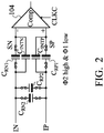
- FIG. 2 shows the connection of the residue capacitor pairs (C RP1 , C RN1 ) and (C RP2 , C RN2 ) when the control signal ⁇ 2 is high and the control signal ⁇ 1 is low.
- the residue capacitors C RP2 and C RN2 are coupled in parallel between the terminals IP and IN in a reverse direction with respect to each other.
- the residue capacitor C RP2 samples the residue voltage V R and the capacitor C RN2 samples the negative value of the residue voltage V R .
- the top plate and the bottom plate of the residue capacitor C RP2 are coupled to the terminals IP and IN, respectively.
- the top plate and the bottom plate of the capacitor C RN2 are coupled to the terminals IN and IP, respectively.
- the residue capacitors C RP1 and C RN1 are coupled to the integral capacitors C INTP and C INTN for residue integral.
- the top plate and the bottom plate of the residue capacitor C RP1 are coupled to the top plate and the bottom plate of the integral capacitor C INTP , respectively.
- the top plate and the bottom plate of the capacitor C RN1 are coupled to the top plate and the bottom plate of the integral capacitor C INTN , respectively.
- FIG. 1 and FIG. 2 show Ping-Pong switching of the residue capacitor pairs (C RP1 , C RN1 ) and (C RP2 , C RN2 ).
- FIG. 3 is a timing diagram of the control signals CLKS, CLKC, ⁇ 1 and ⁇ 2.
- the control signal CLKS is high, the input sampling phase for the input voltage V I is performed. Following the input sampling phase is the analog-to-digital conversion phase.
- the control signal CLKC oscillates during the analog-to-digital conversion phase. Without using any additional timing slots, the noise-shaping compensation including residue sampling and residue integral is performed during the input sampling phase and the analog-to-digital conversion phase. The sampling rate is improved.
- FIG. 3 there is a first input sampling phase 302, a first analog-to-digital conversion phase 304, a second input sampling phase 306 and a second analog-to-digital conversion phase 308.
- a residue sampling phase is implemented by the residue capacitor pair (C RP1 , C RN1 ) and a residue integral phase is implemented by the residue capacitor pair (C RP2 , C RN2 ), the two phases overlapping the first input sampling phase 302 and the first analog-to-digital conversion phase 304.
- a residue integral phase is implemented by the residue capacitor pair (C RP1 , C RN1 ) and a residue sampling phase is implemented by the residue capacitor pair (C RP2 , C RN2 ), the two phases overlapping the second input sampling phase 306 and the second analog-to-digital conversion phase 308. No additional timing slots are required for the residue sampling and residue integral.
- control signal ⁇ 1 is asserted after the control signal CLKS is asserted and prior to the oscillating of the control signal CLKC.
- the control signal ⁇ 1 is de-asserted before the next asserting of the control signal CLKC.
- the control signal ⁇ 2 is asserted after the asserting for the input sampling phase 306 and prior to the oscillating of the control signal CLKC, and is de-asserted before the next asserting of the control signal CLKC.
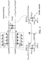
- FIG. 4 details the signals at the different circuit terminals.
- the residue component V RP (i) is V CM + ⁇ V R (i)/2.
- the residue component V RN (i) is V CM - ⁇ V R (i)/2.
- the residue capacitor pair (C RP , C RN ) is switched between residue sampling and residue integral.
- the residue voltage ⁇ V R (i) is captured by the residue capacitor pair (C RP , C RN ).
- the residue capacitors C RP and C RN are connected in parallel between the terminals IP and IN in opposite directions.
- the residue capacitor C RP samples a positive value of the residue voltage ⁇ V R (i) while the capacitor C RN samples a negative value of the residue voltage ⁇ V R (i).
- the residue capacitors C RP and C RN are connected to the positive and negative input terminals of the comparator 104, respectively.
- the sampled residue voltage ⁇ V R (i) is added to the positive input of the comparator 104, and subtracted from the negative input of the comparator 104.
- the output pair IP(i+1) and IN(i+1) of the CDAC 102 is also coupled to the same input pair SP(i+1) and SN(i+1) of the comparator 104 through the integral capacitor pairs (C INTP and C INTN ) and residue capacitor pairs (C RP , C RN ).
- the residue voltage ⁇ V R (i) is doubled without using any operational amplifier. And there is no need to use an additional comparator input pair with larger transistor size for the amplification of the residue voltage ⁇ V R (i).
- FIG. 5 is a block diagram depicting the transfer function of the NS-SAR ADC 100.
- the passive integration (capacitor sharing between C RES and C INT ) makes the factor a smaller than 1, where a is C RES / (C RES + C INT ).
- the sampled residue voltage is amplified without op amplifier or additional large-sized comparator input pair.
- the NS-SAR ADC 100 compensates for the noise according to the sampled residue voltage. Specifically, the residue voltage is sampled without the component of the common-mode voltage VCM. Thus, the NS-SAR ADC 100 is not only compatible with the successive approximation based on a stable common-mode voltage VCM as shown in ( FIG. 6A ), but also works well for successive approximation based on the changing common-mode voltage VCM ( FIG. 6B ).
- the CDAC 102 operates at a stable common mode voltage V CM . In another exemplary embodiment, the CDAC 102 operates at a changing common mode voltage V CM for single-side successive approximation.
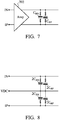
- FIG. 7 depicts another residue sampling design in accordance with an exemplary embodiment of the present invention.
- An amplifier 702 is introduced to amplify the residue voltage between the two terminals IP and IN of the CDAC 102.
- FIG. 8 depicts another residue sampling design in accordance with an exemplary embodiment of the present invention.
- the residue sampling is further controlled by a direct current voltage VDC.
- each residue capacitor includes two capacitors (two residue capacitors 2C RP /two capacitors 2C RN ) connected in series with a connection terminal coupled to a direct current voltage VDC.
Landscapes
- Engineering & Computer Science (AREA)
- Theoretical Computer Science (AREA)
- Analogue/Digital Conversion (AREA)
Abstract
Description
- The present invention relates to analog-to-digital converters (ADCs).
- SAR ADCs (successive approximation analog-to-digital converters) are popular in mobile WiFi applications due to their low power and small area. An SNR (signal-to-noise ratio) of 60-70dB is necessary to meet the noise budget for the downlink chain in the 802.11 ac/ax standards. Comparator noise and quantization noise are typically the dominant noise sources limiting the SNR. Recently, noise-shaping SAR (NS-SAR) ADCs have become popular to increase SNR, which considerably reduce these two noise sources.
- A basic concept of SAR ADC is described in this paragraph. During an input sampling phase, an input voltage VI is sampled onto a weighted capacitor array (capacitive digital-to-analog converter, abbreviated to CDAC). During an analog-to-digital conversion phase, a successive approximation scheme is performed. The CDAC is controlled by digital signals for successive approximation that is performed based on the sampled input voltage VI. A comparator operates according to the CDAC to change the digital signals controlling the CDAC. According to a series of comparator outputs, the capacitors within the CDAC are switched between several reference voltages to equalize the voltage levels at the positive and negative output terminals of the CDAC, and the digital representation of the input voltage VI is determined from the MSB (most significant bit) to the LSB (least significant bit). A residue voltage VR may still exist between the positive and negative output terminal of the CDAC after the successive approximation. A noise-shaping signal may be derived from the residue voltage VR for noise elimination. The comparator of the SAR ADC (SAR comparator) usually provides an additional differential input pair for subtraction of the noise-shaping signal. The additional differential input pair, however, may contribute extra thermal and kickback noise.
- Furthermore, the generation of the noise-shaping signal may involve a charge-sharing procedure. An active residue amplification (using an op amp) is usually used to maintain the residue amplitude, which consumes a lot of power. As for a passive solution (without the op amp), a gain ratio between the signal and residue input pairs of the SAR comparator is required, which results in a large-sized SAR comparator. Specifically, for a higher order noise shaping, the charge-sharing procedure may repeat and the SAR comparator may require more input pairs. In conventional techniques, extra timing slots are required for the charge-sharing procedure, which also limits the sampling rate of the NS-SAR ADC.
- An efficient, low power and small area NS-SAR ADC is called for.
- A noise-shaping successive approximation analog-to-digital converter (NS-SAR ADC) using a passive noise-shaping technique with 1-input-pair SAR comparator is introduced.
- An analog-to-digital converter (ADC) in accordance with an exemplary embodiment of the present invention includes a digital-to-analog converter (DAC), a comparator, and a residue sampling and integration circuit. The DAC samples an input signal according to a first control signal. The comparator operates according to the DAC to change the first control signal controlling the DAC, and for generating digital representation of the input signal. The residue sampling and integration circuit is coupled between the DAC and the comparator, for sampling a residue voltage generated by the DAC and charge-sharing of the sampled residue voltage.
- In an exemplary embodiment, the residue sampling and integration circuit includes a first integral capacitor and a first residue capacitor. The first integral capacitor is coupled between a first input terminal of the comparator and a first output terminal of the DAC. After the first residue capacitor samples a residue voltage generated by the DAC, the first residue capacitor is coupled to the first integral capacitor for charge-sharing of the residue voltage.
- In an exemplary embodiment, the residue sampling and integration circuit further includes a second integral capacitor and a second residue capacitor. The second integral capacitor is coupled between a second input terminal of the comparator and a second output terminal of the DAC. After the second residue capacitor samples a value of the residue voltage, the second residue capacitor is coupled to the second integral capacitor for charge-sharing of the residue voltage.
- In an exemplary embodiment, when sampling the residue voltage, a top plate of the first residue capacitor is coupled to the first output terminal of the DAC and a bottom plate of the first residue capacitor is coupled to the second output terminal of the DAC. When sampling the value of the residue voltage, a top plate of the second residue capacitor is coupled to the second output terminal of the DAC and a bottom plate of the second residue capacitor is coupled to the first output terminal of the DAC.
- In an exemplary embodiment, a top plate of the first integral capacitor is coupled to the first input terminal of the comparator and a bottom plate of the first integral capacitor is coupled to the first output terminal of the DAC. A top plate of the second integral capacitor is coupled to the second input terminal of the comparator and a bottom plate of the second integral capacitor is coupled to the second output terminal of the DAC.
- In an exemplary embodiment, when the first residue capacitor is coupled to the first integral capacitor for charge-sharing of the residue voltage, the top plate of the first residue capacitor is coupled to the top plate of the first integral capacitor and the bottom plate of the first residue capacitor is coupled to the bottom plate of the first integral capacitor. When the second residue capacitor is coupled to the second integral capacitor for charge-sharing of the residue voltage, the top plate of the second residue capacitor is coupled to the top plate of the second integral capacitor and the bottom plate of the second residue capacitor is coupled to the bottom plate of the second integral capacitor.
- In an exemplary embodiment, a first input sampling phase, a first analog-to-digital conversion phase, and a first residue sampling phase are arranged. During the first input sampling phase, the DAC samples the input voltage. During the first analog-to-digital conversion phase, the successive approximation is performed. During the first residue sampling phase, the first residue capacitor samples the residue voltage and the second residue capacitor samples the value of the residue voltage. The first residue sampling phase overlaps the first input sampling phase and the first analog-to-digital conversion phase without using additional timing slots.
- In an exemplary embodiment, a second input sampling phase, a second analog-to-digital conversion phase, and a first residue integral phase are additionally arranged. During the second input sampling phase following the first analog-to-digital conversion phase, the DAC samples the input voltage again. During the second analog-to-digital conversion phase following the second input sampling phase, the successive approximation is performed again. During the first residue integral phase, the first residue capacitor is coupled to the first integral capacitor and the second residue capacitor is coupled to the second integral capacitor for charge-sharing of the residue voltage. The first residue integral phase overlaps the second input sampling phase and the second analog-to-digital conversion phase without using additional timing slots.
- In an exemplary embodiment, the residue sampling and integration circuit further includes a third residue capacitor and a fourth residue capacitor, for Ping-Pong mode operations.
- In an exemplary embodiment, the DAC operates at a stable common-mode voltage.
- In an exemplary embodiment, the DAC operates at a changing common-mode voltage for single-side successive approximation.
- In an exemplary embodiment, the ADC further includes an amplifier. The amplifier has input terminals coupled to the first output terminal and the second output terminal of the DAC, and has output terminals coupled to the first integral capacitor and the second integral capacitor.
- In an exemplary embodiment, the first residue capacitor is formed by two capacitors connected in series with a connection terminal coupled to a direct current voltage, and the second residue capacitor is formed by two capacitors connected in series with a connection terminal coupled to the direct current voltage.
- A detailed description is given in the following embodiments with reference to the accompanying drawings.
- The present invention can be more fully understood by reading the subsequent detailed description and examples with references made to the accompanying drawings, wherein:
-
FIG. 1 depicts a NS-SAR ADC (noise-shaping successive approximation analog-to-digital converter) 100 in accordance with an exemplary embodiment of the present invention; -
FIG. 2 shows the connection of the residue capacitor pairs (CRP1, CRN1) and (CRP2, CRN2) when the control signal Φ2 is high and the control signal Φ1 is low; -
FIG. 3 is a timing diagram of the control signals CLKS, CLKC, Φ1 and Φ2; -
FIG. 4 details the signals at the different circuit terminals; -
FIG. 5 is a block diagram depicting the transfer function of the NS-SARADC 100; and -
FIG. 6A shows successive approximation based on a stable common-mode voltage VCM andFIG. 6B shows successive approximation based on a changing common-mode voltage VCM; -
FIG. 7 depicts another residue sampling design in accordance with an exemplary embodiment of the present invention, wherein anamplifier 702 is introduced to amplify the residue voltage between the two terminals IP and IN of theCDAC 102; and -
FIG. 8 depicts another residue sampling design in accordance with an exemplary embodiment of the present invention, wherein the residue sampling is further controlled by a DC voltage VDC. - The following description shows exemplary embodiments carrying out the invention. This description is made for the purpose of illustrating the general principles of the invention and should not be taken in a limiting sense. The scope of the invention is best determined by reference to the appended claims.
-
FIG. 1 depicts a NS-SAR ADC (noise-shaping successive approximation analog-to-digital converter) 100 in accordance with an exemplary embodiment of the present invention. - The NS-
SAR ADC 100 includes a CDAC (capacitive digital-to-analog converter) 102, a comparator (as known as a SAR comparator) 104, aSAR logic unit 106 and adecoder 108. TheCDAC 102 is a weighted capacitor array. During an input sampling phase (corresponding to a high status of the control signal CLKS), an input voltage VI (=VIP-VIN) is sampled onto the weighted capacitor array (CDAC 102). The top plates (corresponding to terminals IP and IN) of theCDAC 102 are coupled to thecomparator 104. During an analog-to-digital conversion phase (corresponding to a series of pulses of the control signal CLKC), a series of comparator outputs are generated and sent to theSAR logic unit 106. Accordingly, theSAR logic unit 106 switches the reference voltages coupled to the capacitors of theCDAC 102 to achieve the successive approximation between the two terminals IP and IN. The successive approximation controlled by theSAR logic unit 106 is decoded by thedecoder 108. A digital representation Dout of the input voltage VI (=VIP-VIN) is generated. - The NS-
SAR ADC 100 includes a residue sampling andintegration circuit 110. The residue sampling andintegration circuit 110 includes a residue capacitor pair (CRP1, CRNI), a residue capacitor pair (CRP2, CRN2) and an integral capacitor pair (CINTP and CINTN). A residue voltage (VR) between the two terminals IP and IN is sampled selectively by the residue capacitor pair (CRP1, CRN1) or the residue capacitor pair (CRP2, CRN2), and is integrated into the integral capacitor pair (CINTP and CINTN) by charge sharing. The integral capacitor CINTP is configured between the terminal IP and positive input terminal '+' (or SP) of thecomparator 104 with the top plate coupled to the positive input terminal '+' and the bottom plate coupled to the terminal IP. Another integral capacitor CINTN is configured between the terminal IN and negative input terminal '-'(or SN) of thecomparator 104 with the top plate coupled to the negative input terminal '-' and the bottom plate coupled to the terminal IN. The residue capacitor pairs (CRP1, CRN1) and (CRP2, CRN2) are utilized in a Ping-Pong mode, switched according to control signals Φ1 and Φ2. - In
FIG. 1 , the control signal Φ1 is high and the control signalΦ2 is low. The residue capacitors CRP1 and CRN1 are coupled in parallel between the terminals IP and IN in a reverse direction with respect to each other. The residue capacitor CRP1 samples the residue voltage VR and the capacitor CRN1 samples the negative value of the residue voltage VR. The top plate and the bottom plate of the residue capacitor CRP1 are coupled to the terminals IP and IN, respectively. The top plate and the bottom plate of the capacitor CRN1 are coupled to the terminals IN and IP, respectively. As for the residue capacitor pair (CRP2, CRN2), the previous residue voltage sampled in the residue capacitor CRP2 and the negative value of the previous residue voltage sampled in the capacitor CRN2. As shown, and the residue capacitors CRP2 and CRN2 are coupled to the integral capacitors CINTP and CINTN for residue integral. The top plate and the bottom plate of the residue capacitor CRP2 are coupled to the top plate and the bottom plate of the integral capacitor CINTP, respectively. The top plate and the bottom plate of the capacitor CRN2 are coupled to the top plate and the bottom plate of the integral capacitor CINTN, respectively. - Specifically, the
comparator 104 includes one input pair. The integral of the residue voltage is added to the voltages at the terminals IP and IN. Instead of arranging additional input pair in thecomparator 104, the noise-shaping signal is directly compensated on the voltages retrieved from the terminals IP and IN. Thecomparator 104 does not require additional input pair for the subtraction of noise-shaping signal. -
FIG. 2 shows the connection of the residue capacitor pairs (CRP1, CRN1) and (CRP2, CRN2) when the control signalΦ2 is high and the control signal Φ1 is low. The residue capacitors CRP2 and CRN2 are coupled in parallel between the terminals IP and IN in a reverse direction with respect to each other. The residue capacitor CRP2 samples the residue voltage VR and the capacitor CRN2 samples the negative value of the residue voltage VR. The top plate and the bottom plate of the residue capacitor CRP2 are coupled to the terminals IP and IN, respectively. The top plate and the bottom plate of the capacitor CRN2 are coupled to the terminals IN and IP, respectively. This time, and the residue capacitors CRP1 and CRN1 are coupled to the integral capacitors CINTP and CINTN for residue integral. The top plate and the bottom plate of the residue capacitor CRP1 are coupled to the top plate and the bottom plate of the integral capacitor CINTP, respectively. The top plate and the bottom plate of the capacitor CRN1 are coupled to the top plate and the bottom plate of the integral capacitor CINTN, respectively. -
FIG. 1 andFIG. 2 show Ping-Pong switching of the residue capacitor pairs (CRP1, CRN1) and (CRP2, CRN2). -
FIG. 3 is a timing diagram of the control signals CLKS, CLKC, Φ1 and Φ2. When the control signal CLKS is high, the input sampling phase for the input voltage VI is performed. Following the input sampling phase is the analog-to-digital conversion phase. As shown, the control signal CLKC oscillates during the analog-to-digital conversion phase. Without using any additional timing slots, the noise-shaping compensation including residue sampling and residue integral is performed during the input sampling phase and the analog-to-digital conversion phase. The sampling rate is improved. - In
FIG. 3 , there is a firstinput sampling phase 302, a first analog-to-digital conversion phase 304, a secondinput sampling phase 306 and a second analog-to-digital conversion phase 308.When the control signal Φ1 is high and the control signal Φ2 is low, a residue sampling phase is implemented by the residue capacitor pair (CRP1, CRN1) and a residue integral phase is implemented by the residue capacitor pair (CRP2, CRN2), the two phases overlapping the firstinput sampling phase 302 and the first analog-to-digital conversion phase 304. When the control signal Φ1 is low and the control signalΦ2 is high, a residue integral phase is implemented by the residue capacitor pair (CRP1, CRN1) and a residue sampling phase is implemented by the residue capacitor pair (CRP2, CRN2), the two phases overlapping the secondinput sampling phase 306 and the second analog-to-digital conversion phase 308. No additional timing slots are required for the residue sampling and residue integral. - In the exemplary embodiment of
FIG. 3 , the control signal Φ1 is asserted after the control signal CLKS is asserted and prior to the oscillating of the control signal CLKC. The control signal Φ1 is de-asserted before the next asserting of the control signal CLKC. The control signalΦ2 is asserted after the asserting for theinput sampling phase 306 and prior to the oscillating of the control signal CLKC, and is de-asserted before the next asserting of the control signal CLKC. -
FIG. 4 details the signals at the different circuit terminals. At terminal IP, the residue component VRP(i) is VCM + ΔVR(i)/2. At terminal IN, the residue component VRN(i) is VCM - ΔVR(i)/2. By setting the control signal (Φ1/Φ2), the residue capacitor pair (CRP, CRN) is switched between residue sampling and residue integral. - Through the residue sampling, the residue voltageΔVR(i) is captured by the residue capacitor pair (CRP, CRN). The residue capacitors CRP and CRN are connected in parallel between the terminals IP and IN in opposite directions. The residue capacitor CRP samples a positive value of the residue voltageΔVR(i) while the capacitor CRN samples a negative value of the residue voltageΔVR(i).
- When switching the residue capacitor pair (CRP, CRN) for residue integral, the residue capacitors CRP and CRN are connected to the positive and negative input terminals of the
comparator 104, respectively. The sampled residue voltageΔVR(i) is added to the positive input of thecomparator 104, and subtracted from the negative input of thecomparator 104. - Specifically, the output pair IP(i+1) and IN(i+1) of the
CDAC 102 is also coupled to the same input pair SP(i+1) and SN(i+1) of thecomparator 104 through the integral capacitor pairs (CINTP and CINTN) and residue capacitor pairs (CRP, CRN). As shown, the voltage level at the positive and negative input terminals of thecomparator 104 are:

-
FIG. 5 is a block diagram depicting the transfer function of the NS-SAR ADC 100. The passive integration (capacitor sharing between CRES and CINT) makes the factor a smaller than 1, where a is CRES / (CRES+ CINT). Specifically, the sampled residue voltage is amplified without op amplifier or additional large-sized comparator input pair. When a is 0.5 and g is 2, the transfer function of the NS-SAR ADC 100 is:
- The NS-
SAR ADC 100 compensates for the noise according to the sampled residue voltage. Specifically, the residue voltage is sampled without the component of the common-mode voltage VCM. Thus, the NS-SAR ADC 100 is not only compatible with the successive approximation based on a stable common-mode voltage VCM as shown in (FIG. 6A ), but also works well for successive approximation based on the changing common-mode voltage VCM (FIG. 6B ). - In an exemplary embodiment, the
CDAC 102 operates at a stable common mode voltage VCM. In another exemplary embodiment, theCDAC 102 operates at a changing common mode voltage VCM for single-side successive approximation. -
FIG. 7 depicts another residue sampling design in accordance with an exemplary embodiment of the present invention. Anamplifier 702 is introduced to amplify the residue voltage between the two terminals IP and IN of theCDAC 102. -
FIG. 8 depicts another residue sampling design in accordance with an exemplary embodiment of the present invention. The residue sampling is further controlled by a direct current voltage VDC. As shown, each residue capacitor includes two capacitors (two residue capacitors 2CRP/two capacitors 2CRN) connected in series with a connection terminal coupled to a direct current voltage VDC. - While the invention has been described by way of example and in terms of the preferred embodiments, it should be understood that the invention is not limited to the disclosed embodiments. On the contrary, it is intended to cover various modifications and similar arrangements (as would be apparent to those skilled in the art). Therefore, the scope of the appended claims should be accorded the broadest interpretation so as to encompass all such modifications and similar arrangements.
Claims (15)
- An analog-to-digital converter (100), comprising:a digital-to-analog converter (102), for sampling an input signal (VI) according to a first control signal (CLKS);a comparator (104), operating according to the digital-to-analog converter to change the first control signal controlling the digital-to-analog converter, and for generating digital representation (Dout) of the input signal;a residue sampling and integration circuit (110), coupled between the digital-to-analog converter and the comparator, for sampling a residue voltage generated by the digital-to-analog converter and charge-sharing of the sampled residue voltage.
- The analog-to-digital converter as claimed in claim 1, wherein the residue sampling and integration circuit comprises:a first integral capacitor (CINTP), coupled between a first input terminal (+) of the comparator and a first output terminal of the digital-to-analog converter; anda first residue capacitor (CRP1), wherein after the first residue capacitor samples the residue voltage generated by the digital-to-analog converter, the first residue capacitor is coupled to the first integral capacitor for charge-sharing of the residue voltage.
- The analog-to-digital converter as claimed in claim 2, wherein the residue sampling and integration circuit further comprises:a second integral capacitor (CINTN), coupled between a second input terminal (-) of the comparator and a second output terminal of the digital-to-analog converter; anda second residue capacitor (CRN1), wherein after the second residue capacitor samples a value related to the residue voltage, the second residue capacitor is coupled to the second integral capacitor for charge-sharing of the residue voltage.
- The analog-to-digital converter as claimed in claim 3, wherein:when sampling the residue voltage, a top plate of the first residue capacitor is coupled to the first output terminal of the digital-to-analog converter and a bottom plate of the first residue capacitor is coupled to the second output terminal of the digital-to-analog converter; andwhen sampling the value related to the residue voltage, a top plate of the second residue capacitor is coupled to the second output terminal of the digital-to-analog converter and a bottom plate of the second residue capacitor is coupled to the first output terminal of the digital-to-analog converter.
- The analog-to-digital converter as claimed in claim 4, wherein:a top plate of the first integral capacitor is coupled to the first input terminal of the comparator and a bottom plate of the first integral capacitor is coupled to the first output terminal of the digital-to-analog converter;a top plate of the second integral capacitor is coupled to the second input terminal of the comparator and a bottom plate of the second integral capacitor is coupled to the second output terminal of the digital-to-analog converter;when the first residue capacitor is coupled to the first integral capacitor for charge-sharing of the residue voltage, the top plate of the first residue capacitor is coupled to the top plate of the first integral capacitor and the bottom plate of the first residue capacitor is coupled to the bottom plate of the first integral capacitor; andwhen the second residue capacitor is coupled to the second integral capacitor for charge-sharing of the residue voltage, the top plate of the second residue capacitor is coupled to the top plate of the second integral capacitor and the bottom plate of the second residue capacitor is coupled to the bottom plate of the second integral capacitor.
- The analog-to-digital converter as claimed in claim 5, wherein:during a first input sampling phase (302), the digital-to-analog converter samples the input voltage;during a first analog-to-digital conversion phase (304), successive approximation is performed;during a first residue sampling phase, the first residue capacitor samples the residue voltage and the second residue capacitor samples the value related to the residue voltage, and the first residue sampling phase overlaps the first input sampling phase and the first analog-to-digital conversion phase without using additional timing slots;during a second input sampling phase (306) following the first analog-to-digital conversion phase, the digital-to-analog converter samples the input voltage again;during a second analog-to-digital conversion phase (308) following the second input sampling phase, the successive approximation is performed again; andduring a first residue integral phase, the first residue capacitor is coupled to the first integral capacitor and the second residue capacitor is coupled to the second integral capacitor for charge-sharing of the residue voltage, and the first residue integral phase overlaps the second input sampling phase and the second analog-to-digital conversion phase without using additional timing slots.
- The analog-to-digital converter as claimed in claim 6, wherein the residue sampling and integration circuit further comprises:a third residue capacitor (CRP2); anda fourth residue capacitor (CRN2),wherein:when the first residue capacitor finishes sampling the residue voltage and the second residue capacitor finishes sampling the value related to the residue voltage, the third residue capacitor is switched to sample the residue voltage and the fourth residue capacitor is switched to sample the value related to the residue voltage;when the first residue capacitor is switched back to sample the residue voltage, a top plate of the third residue capacitor is coupled to the first input terminal of the comparator and a bottom plate of the third residue capacitor is coupled to the first output terminal of the digital-to-analog converter;when the second residue capacitor is switched back to sample the value related to the residue voltage, a top plate of the fourth residue capacitor is coupled to the second input terminal of the comparator and a bottom plate of the fourth residue capacitor is coupled to the second output terminal of the digital-to-analog converter;when using the third residue capacitor to sample the residue voltage, the top plate of the third residue capacitor is coupled to the first output terminal of the digital-to-analog converter and the bottom plate of the third residue capacitor is coupled to the second output terminal of the digital-to-analog converter; andwhen using the fourth residue capacitor to sample the value related to the residue voltage, the top plate of the fourth residue capacitor is coupled to the second output terminal of the digital-to-analog converter and the bottom plate of the fourth residue capacitor is coupled to the first output terminal of the digital-to-analog converter.
- The analog-to-digital converter as claimed in claim 7, wherein:during a second residue sampling phase, the third residue capacitor samples the residue voltage and the fourth residue capacitor samples the value related to the residue voltage; andthe second residue sampling phase overlaps the second input sampling phase and the second analog-to-digital conversion phase without using additional timing slots.
- The analog-to-digital converter as claimed in claim 8, wherein:the first control signal is asserted during the first input sampling phase and the second input sampling phase;the comparator compares signals at the first and second input terminals when a second control signal (CLKC) is asserted;the second control signal oscillates between high and low during the first analog-to-digital conversion phase;the second control signal oscillates between high and low during the second analog-to-digital conversion phase;the first residue sampling phase starts by asserting a third control signal (Φ1) and finishes by de-asserting the third control signal; andthe third control signal is asserted after a first assertion of the first control signal and prior to oscillating of the second control signal, and is de-asserted before a second assertion of the second control signal.
- The analog-to-digital converter as claimed in claim 9, wherein:the second residue sampling phase starts by asserting a fourth control signal (Φ2) and finishes by de-asserting the fourth control signal; andthe fourth control signal is asserted after the second asserting of the first control signal and prior to oscillation of the second control signal, and is de-asserted before a third assertion of the second control signal.
- The analog-to-digital converter as claimed in any one of the preceding claims, further comprising:a successive approximation logic unit, coupled to an output terminal of the comparator to generate digital signals controlling the analog-to-digital converter according to the comparator; anda decoder, decoding according to the successive approximation logic unit to generate the digital representation of the input voltage.
- The analog-to-digital converter as claimed in any one of the preceding claims, wherein:
the digital-to-analog converter operates at a stable common-mode voltage. - The analog-to-digital converter as claimed in any one of claims 1 to 11, wherein:
the digital-to-analog converter operates at a changing common-mode voltage for single-side successive approximation. - The analog-to-digital converter as claimed in any one of claims 3 to 10, further comprising:
an amplifier (702), having input terminals coupled to the first output terminal and the second output terminal of the digital-to-analog converter, and having output terminals coupled to the first integral capacitor and the second integral capacitor. - The analog-to-digital converter as claimed in any one of claims 3 to 10, wherein:the first residue capacitor is formed by two capacitors (the pair of 2CRP of FIG. 8) connected in series with a connection terminal coupled to a direct current voltage (VDC); andthe second residue capacitor is formed by two capacitors connected (the pair of 2CRN of FIG. 8) in series with a connection terminal coupled to the direct current voltage.
Applications Claiming Priority (2)
| Application Number | Priority Date | Filing Date | Title |
|---|---|---|---|
| US201862744705P | 2018-10-12 | 2018-10-12 | |
| US16/539,050 US10840932B2 (en) | 2018-10-12 | 2019-08-13 | Analog-to-digital converter |
Publications (2)
| Publication Number | Publication Date |
|---|---|
| EP3637618A1 true EP3637618A1 (en) | 2020-04-15 |
| EP3637618B1 EP3637618B1 (en) | 2023-01-11 |
Family
ID=68242386
Family Applications (1)
| Application Number | Title | Priority Date | Filing Date |
|---|---|---|---|
| EP19202069.1A Active EP3637618B1 (en) | 2018-10-12 | 2019-10-08 | Analog-to-digital converter |
Country Status (4)
| Country | Link |
|---|---|
| US (1) | US10840932B2 (en) |
| EP (1) | EP3637618B1 (en) |
| CN (1) | CN111049526B (en) |
| TW (1) | TWI695587B (en) |
Cited By (1)
| Publication number | Priority date | Publication date | Assignee | Title |
|---|---|---|---|---|
| CN117938156A (en) * | 2024-03-20 | 2024-04-26 | 华南理工大学 | Second-order noise shaping circuit applied to NS SAR ADC |
Families Citing this family (6)
| Publication number | Priority date | Publication date | Assignee | Title |
|---|---|---|---|---|
| CN110113051B (en) * | 2019-05-13 | 2020-03-31 | 深圳锐越微技术有限公司 | Analog-to-digital converter error shaping circuit and successive approximation type analog-to-digital converter |
| JP7573236B2 (en) * | 2020-09-28 | 2024-10-25 | パナソニックIpマネジメント株式会社 | AD converter and sensor system including same |
| CN113437976B (en) * | 2021-04-09 | 2023-04-28 | 深圳市纽瑞芯科技有限公司 | Successive approximation method for tri-state quantization and successive approximation analog-to-digital conversion circuit |
| US11522556B1 (en) * | 2021-07-26 | 2022-12-06 | Qualcomm Incorporated | Noise-shaping successive approximation register (SAR) analog-to-digital converter |
| CN115765745B (en) * | 2022-11-22 | 2026-03-03 | 思瑞浦微电子科技(苏州)股份有限公司 | Hybrid ADC circuit, chip and analog-to-digital conversion method |
| US12476648B2 (en) * | 2023-07-25 | 2025-11-18 | Cypress Semiconductor Corporation | Noise shaping successive-approximation register (SAR) analog-to-digital converter (ADC) |
Family Cites Families (23)
| Publication number | Priority date | Publication date | Assignee | Title |
|---|---|---|---|---|
| WO2011036697A1 (en) * | 2009-09-24 | 2011-03-31 | 株式会社 東芝 | A/d conversion device and radio device |
| US8618975B2 (en) * | 2011-10-26 | 2013-12-31 | Semtech Corporation | Multi-bit successive approximation ADC |
| EP2629426A1 (en) * | 2012-02-17 | 2013-08-21 | Imec | Device, system and method for analogue-to-digital conversion with noise shaping function |
| US9197240B1 (en) * | 2014-07-10 | 2015-11-24 | Taiwan Semiconductor Manufacturing Company, Ltd. | Method and circuit for noise shaping SAR analog-to-digital converter |
| CN106209104A (en) * | 2015-05-27 | 2016-12-07 | 松下知识产权经营株式会社 | Analog-digital converter |
| US9425818B1 (en) * | 2015-05-28 | 2016-08-23 | Qualcomm Incorporated | Noise shaping successive approximation register analog-to-digital converter |
| US9722746B2 (en) * | 2015-09-22 | 2017-08-01 | Mediatek Inc. | Analog-to-digital converter with bandpass noise transfer function |
| WO2017079514A1 (en) * | 2015-11-04 | 2017-05-11 | Board Of Regents, The University Of Texas System | Noise-shaping successive-approximation-register analog-to-digital converter |
| JP2017168930A (en) * | 2016-03-14 | 2017-09-21 | 株式会社東芝 | Switched capacitor circuit |
| US10340932B2 (en) * | 2016-04-29 | 2019-07-02 | Analog Devices, Inc. | Techniques for power efficient oversampling successive approximation register |
| WO2017195911A1 (en) | 2016-05-10 | 2017-11-16 | 서강대학교 산학협력단 | Sar adc to which secondary noise shaping technique is applied |
| US10003348B2 (en) | 2016-09-08 | 2018-06-19 | Mediatek Inc. | Analog-to-digital converter with noise shaping |
| US9698805B1 (en) * | 2016-09-09 | 2017-07-04 | Analog Devices, Inc. | Electrical noise reduction in an analog-to-digital converter |
| US9973202B2 (en) * | 2016-09-20 | 2018-05-15 | Kabushiki Kaisha Toshiba | Successive approximation register analog-to-digital converter |
| US9774345B1 (en) * | 2016-09-20 | 2017-09-26 | Kabushiki Kaisha Toshiba | Successive approximation register analog-to-digital converter |
| CN110089108B (en) * | 2016-12-21 | 2021-07-09 | 奥林巴斯株式会社 | Imaging element, imaging device, and endoscope |
| WO2018116540A1 (en) * | 2016-12-21 | 2018-06-28 | オリンパス株式会社 | Successive approximation a/d conversion device, imaging apparatus, endoscope and setting method |
| US10110242B2 (en) * | 2016-12-27 | 2018-10-23 | Mediatek Inc. | Interleaving successive approximation analog-to-digital converter with noise shaping |
| TWI653836B (en) * | 2017-08-15 | 2019-03-11 | 瑞昱半導體股份有限公司 | Correcting device of successive approximation analog-to-digital conversion |
| KR101840683B1 (en) * | 2017-09-27 | 2018-03-21 | 포항공과대학교 산학협력단 | Sar trpe analog to digital converter using residue integration |
| EP3503407B1 (en) * | 2017-12-19 | 2021-04-07 | IMEC vzw | Improvements in or related to analog-to-digital converters |
| US10547322B2 (en) * | 2018-01-02 | 2020-01-28 | Samsung Electronics Co., Ltd. | Analog-digital converter having multiple feedback, and communication device including the analog-digital converter |
| US10608655B1 (en) * | 2018-12-06 | 2020-03-31 | Analog Devices, Inc. | Inter-stage gain calibration in double conversion analog-to-digital converter |
-
2019
- 2019-08-13 US US16/539,050 patent/US10840932B2/en active Active
- 2019-09-25 CN CN201910913035.7A patent/CN111049526B/en active Active
- 2019-09-27 TW TW108135106A patent/TWI695587B/en active
- 2019-10-08 EP EP19202069.1A patent/EP3637618B1/en active Active
Non-Patent Citations (5)
| Title |
|---|
| GHAEDRAHMATI HANIE ET AL: "160 MS/s 20 MHz bandwidth third-order noise shaping SAR ADC", ELECTRONICS LETTERS, IEE STEVENAGE, GB, vol. 54, no. 3, 8 February 2018 (2018-02-08), pages 128 - 130, XP006075524, ISSN: 0013-5194, DOI: 10.1049/EL.2017.3969 * |
| LIN YING-ZU ET AL: "A 2.4-mW 25-MHz BW 300-MS/s passive noise shaping SAR ADC with noise quantizer technique in 14-nm CMOS", 2017 SYMPOSIUM ON VLSI CIRCUITS, JSAP, 5 June 2017 (2017-06-05), XP033141448, DOI: 10.23919/VLSIC.2017.8008491 * |
| PARK HANGUE ET AL: "A 13-bit noise shaping SAR-ADC with dual-polarity digital calibration", ANALOG INTEGRATED CIRCUITS AND SIGNAL PROCESSING, SPRINGER NEW YORK LLC, US, vol. 75, no. 3, 27 February 2013 (2013-02-27), pages 459 - 465, XP035311706, ISSN: 0925-1030, [retrieved on 20130227], DOI: 10.1007/S10470-013-0050-X * |
| SAISUNDAR S ET AL: "A rail-to-rail noise-shaping non-binary SAR ADC", 2016 INTERNATIONAL SYMPOSIUM ON INTEGRATED CIRCUITS (ISIC), IEEE, 12 December 2016 (2016-12-12), pages 1 - 4, XP033052589, DOI: 10.1109/ISICIR.2016.7829678 * |
| SHI LUKANG ET AL: "A 13b-ENOB Noise Shaping SAR ADC with a Two-Capacitor DAC", 2018 IEEE 61ST INTERNATIONAL MIDWEST SYMPOSIUM ON CIRCUITS AND SYSTEMS (MWSCAS), IEEE, 5 August 2018 (2018-08-05), pages 153 - 156, XP033508775, DOI: 10.1109/MWSCAS.2018.8623994 * |
Cited By (1)
| Publication number | Priority date | Publication date | Assignee | Title |
|---|---|---|---|---|
| CN117938156A (en) * | 2024-03-20 | 2024-04-26 | 华南理工大学 | Second-order noise shaping circuit applied to NS SAR ADC |
Also Published As
| Publication number | Publication date |
|---|---|
| US20200119744A1 (en) | 2020-04-16 |
| US10840932B2 (en) | 2020-11-17 |
| CN111049526A (en) | 2020-04-21 |
| TWI695587B (en) | 2020-06-01 |
| TW202015344A (en) | 2020-04-16 |
| EP3637618B1 (en) | 2023-01-11 |
| CN111049526B (en) | 2023-11-03 |
Similar Documents
| Publication | Publication Date | Title |
|---|---|---|
| EP3637618B1 (en) | Analog-to-digital converter | |
| Ramkaj et al. | A 1.25-GS/s 7-b SAR ADC with 36.4-dB SNDR at 5 GHz using switch-bootstrapping, USPC DAC and triple-tail comparator in 28-nm CMOS | |
| US9847790B2 (en) | Hybrid analog-to-digital converter using digital slope analog-to-digital converter and related hybrid analog-to-digital conversion method thereof | |
| US9136867B2 (en) | ΔΣ-modulator and ΔΣ-A/D converter | |
| US6784824B1 (en) | Analog-to-digital converter which is substantially independent of capacitor mismatch | |
| US7796077B2 (en) | High speed high resolution ADC using successive approximation technique | |
| EP3090488B1 (en) | Combining a coarse adc and a sar adc | |
| US7075471B1 (en) | Double-sampled, time-interleaved analog to digital converter | |
| EP3567720B1 (en) | Mismatch and reference common-mode offset insensitive single-ended switched capacitor gain stage | |
| US7187318B1 (en) | Pipeline ADC using multiplying DAC and analog delay circuits | |
| US7852254B1 (en) | 1-bit cell circuit used in a pipelined analog to digital converter | |
| US10547321B2 (en) | Method and apparatus for enabling wide input common-mode range in SAR ADCS with no additional active circuitry | |
| US10090851B2 (en) | Successive approximation type analog-to-digital (A/D) converter | |
| US6756928B2 (en) | Pseudo-differential amplifier and analog-to-digital converter using the same | |
| EP2894787A1 (en) | High-speed successive approximation analog-to-digital converter | |
| CN102640228A (en) | Input configuration for analog to digital converter | |
| JP4454498B2 (en) | Switched capacitor systems, methods and uses | |
| US12592717B2 (en) | Integrator circuit | |
| US7907078B2 (en) | Analog-to-digital converter and analog to-digital conversion method | |
| US6490332B1 (en) | High speed, low-power shift register and circuits and methods using the same | |
| US11165435B2 (en) | Signal converting apparatus | |
| Cho | A 2.24-mW, 61.8-dB SNDR, 20-MS/s pipelined ADC with charge-pump-based dynamic biasing for power reduction in op amp sharing | |
| Dong et al. | An 11.36-Bit 405 μW SAR-VCO ADC with single-path differential VCO-based quantizer in 65 nm CMOS | |
| KR20230114464A (en) | A double edge trigger, performance-aware SAR ADC | |
| Zhang et al. | A 20kHz 87.2 dB SNDR 12.1 µW NS SAR ADC Based on Quantization-Error-Matched RLSB-First Algorithm |
Legal Events
| Date | Code | Title | Description |
|---|---|---|---|
| PUAI | Public reference made under article 153(3) epc to a published international application that has entered the european phase |
Free format text: ORIGINAL CODE: 0009012 |
|
| STAA | Information on the status of an ep patent application or granted ep patent |
Free format text: STATUS: THE APPLICATION HAS BEEN PUBLISHED |
|
| AK | Designated contracting states |
Kind code of ref document: A1 Designated state(s): AL AT BE BG CH CY CZ DE DK EE ES FI FR GB GR HR HU IE IS IT LI LT LU LV MC MK MT NL NO PL PT RO RS SE SI SK SM TR |
|
| AX | Request for extension of the european patent |
Extension state: BA ME |
|
| STAA | Information on the status of an ep patent application or granted ep patent |
Free format text: STATUS: REQUEST FOR EXAMINATION WAS MADE |
|
| 17P | Request for examination filed |
Effective date: 20200814 |
|
| RBV | Designated contracting states (corrected) |
Designated state(s): AL AT BE BG CH CY CZ DE DK EE ES FI FR GB GR HR HU IE IS IT LI LT LU LV MC MK MT NL NO PL PT RO RS SE SI SK SM TR |
|
| STAA | Information on the status of an ep patent application or granted ep patent |
Free format text: STATUS: EXAMINATION IS IN PROGRESS |
|
| 17Q | First examination report despatched |
Effective date: 20220111 |
|
| RIC1 | Information provided on ipc code assigned before grant |
Ipc: H03M 1/46 20060101ALN20220516BHEP Ipc: H03M 1/08 20060101AFI20220516BHEP |
|
| RIC1 | Information provided on ipc code assigned before grant |
Ipc: H03M 1/46 20060101ALN20220711BHEP Ipc: H03M 1/08 20060101AFI20220711BHEP |
|
| GRAP | Despatch of communication of intention to grant a patent |
Free format text: ORIGINAL CODE: EPIDOSNIGR1 |
|
| STAA | Information on the status of an ep patent application or granted ep patent |
Free format text: STATUS: GRANT OF PATENT IS INTENDED |
|
| RIC1 | Information provided on ipc code assigned before grant |
Ipc: H03M 1/46 20060101ALN20220815BHEP Ipc: H03M 1/08 20060101AFI20220815BHEP |
|
| RIC1 | Information provided on ipc code assigned before grant |
Ipc: H03M 1/46 20060101ALN20220907BHEP Ipc: H03M 1/08 20060101AFI20220907BHEP |
|
| INTG | Intention to grant announced |
Effective date: 20220919 |
|
| RIC1 | Information provided on ipc code assigned before grant |
Ipc: H03M 1/46 20060101ALN20220909BHEP Ipc: H03M 1/08 20060101AFI20220909BHEP |
|
| GRAS | Grant fee paid |
Free format text: ORIGINAL CODE: EPIDOSNIGR3 |
|
| RIN1 | Information on inventor provided before grant (corrected) |
Inventor name: LU, CHAO HSIN Inventor name: TSOU, SHAN-CHIH Inventor name: TSAI, CHIHHOU Inventor name: LIN, CHIN-YU Inventor name: LIN, YING-ZU |
|
| GRAA | (expected) grant |
Free format text: ORIGINAL CODE: 0009210 |
|
| STAA | Information on the status of an ep patent application or granted ep patent |
Free format text: STATUS: THE PATENT HAS BEEN GRANTED |
|
| AK | Designated contracting states |
Kind code of ref document: B1 Designated state(s): AL AT BE BG CH CY CZ DE DK EE ES FI FR GB GR HR HU IE IS IT LI LT LU LV MC MK MT NL NO PL PT RO RS SE SI SK SM TR |
|
| REG | Reference to a national code |
Ref country code: GB Ref legal event code: FG4D |
|
| REG | Reference to a national code |
Ref country code: CH Ref legal event code: EP |
|
| REG | Reference to a national code |
Ref country code: DE Ref legal event code: R096 Ref document number: 602019024234 Country of ref document: DE |
|
| REG | Reference to a national code |
Ref country code: IE Ref legal event code: FG4D |
|
| REG | Reference to a national code |
Ref country code: AT Ref legal event code: REF Ref document number: 1544033 Country of ref document: AT Kind code of ref document: T Effective date: 20230215 |
|
| REG | Reference to a national code |
Ref country code: LT Ref legal event code: MG9D |
|
| REG | Reference to a national code |
Ref country code: NL Ref legal event code: MP Effective date: 20230111 |
|
| REG | Reference to a national code |
Ref country code: AT Ref legal event code: MK05 Ref document number: 1544033 Country of ref document: AT Kind code of ref document: T Effective date: 20230111 |
|
| PG25 | Lapsed in a contracting state [announced via postgrant information from national office to epo] |
Ref country code: NL Free format text: LAPSE BECAUSE OF FAILURE TO SUBMIT A TRANSLATION OF THE DESCRIPTION OR TO PAY THE FEE WITHIN THE PRESCRIBED TIME-LIMIT Effective date: 20230111 |
|
| P01 | Opt-out of the competence of the unified patent court (upc) registered |
Effective date: 20230607 |
|
| PG25 | Lapsed in a contracting state [announced via postgrant information from national office to epo] |
Ref country code: RS Free format text: LAPSE BECAUSE OF FAILURE TO SUBMIT A TRANSLATION OF THE DESCRIPTION OR TO PAY THE FEE WITHIN THE PRESCRIBED TIME-LIMIT Effective date: 20230111 Ref country code: PT Free format text: LAPSE BECAUSE OF FAILURE TO SUBMIT A TRANSLATION OF THE DESCRIPTION OR TO PAY THE FEE WITHIN THE PRESCRIBED TIME-LIMIT Effective date: 20230511 Ref country code: NO Free format text: LAPSE BECAUSE OF FAILURE TO SUBMIT A TRANSLATION OF THE DESCRIPTION OR TO PAY THE FEE WITHIN THE PRESCRIBED TIME-LIMIT Effective date: 20230411 Ref country code: LV Free format text: LAPSE BECAUSE OF FAILURE TO SUBMIT A TRANSLATION OF THE DESCRIPTION OR TO PAY THE FEE WITHIN THE PRESCRIBED TIME-LIMIT Effective date: 20230111 Ref country code: LT Free format text: LAPSE BECAUSE OF FAILURE TO SUBMIT A TRANSLATION OF THE DESCRIPTION OR TO PAY THE FEE WITHIN THE PRESCRIBED TIME-LIMIT Effective date: 20230111 Ref country code: HR Free format text: LAPSE BECAUSE OF FAILURE TO SUBMIT A TRANSLATION OF THE DESCRIPTION OR TO PAY THE FEE WITHIN THE PRESCRIBED TIME-LIMIT Effective date: 20230111 Ref country code: ES Free format text: LAPSE BECAUSE OF FAILURE TO SUBMIT A TRANSLATION OF THE DESCRIPTION OR TO PAY THE FEE WITHIN THE PRESCRIBED TIME-LIMIT Effective date: 20230111 Ref country code: AT Free format text: LAPSE BECAUSE OF FAILURE TO SUBMIT A TRANSLATION OF THE DESCRIPTION OR TO PAY THE FEE WITHIN THE PRESCRIBED TIME-LIMIT Effective date: 20230111 |
|
| PG25 | Lapsed in a contracting state [announced via postgrant information from national office to epo] |
Ref country code: SE Free format text: LAPSE BECAUSE OF FAILURE TO SUBMIT A TRANSLATION OF THE DESCRIPTION OR TO PAY THE FEE WITHIN THE PRESCRIBED TIME-LIMIT Effective date: 20230111 Ref country code: PL Free format text: LAPSE BECAUSE OF FAILURE TO SUBMIT A TRANSLATION OF THE DESCRIPTION OR TO PAY THE FEE WITHIN THE PRESCRIBED TIME-LIMIT Effective date: 20230111 Ref country code: IS Free format text: LAPSE BECAUSE OF FAILURE TO SUBMIT A TRANSLATION OF THE DESCRIPTION OR TO PAY THE FEE WITHIN THE PRESCRIBED TIME-LIMIT Effective date: 20230511 Ref country code: GR Free format text: LAPSE BECAUSE OF FAILURE TO SUBMIT A TRANSLATION OF THE DESCRIPTION OR TO PAY THE FEE WITHIN THE PRESCRIBED TIME-LIMIT Effective date: 20230412 Ref country code: FI Free format text: LAPSE BECAUSE OF FAILURE TO SUBMIT A TRANSLATION OF THE DESCRIPTION OR TO PAY THE FEE WITHIN THE PRESCRIBED TIME-LIMIT Effective date: 20230111 |
|
| REG | Reference to a national code |
Ref country code: DE Ref legal event code: R097 Ref document number: 602019024234 Country of ref document: DE |
|
| PG25 | Lapsed in a contracting state [announced via postgrant information from national office to epo] |
Ref country code: SM Free format text: LAPSE BECAUSE OF FAILURE TO SUBMIT A TRANSLATION OF THE DESCRIPTION OR TO PAY THE FEE WITHIN THE PRESCRIBED TIME-LIMIT Effective date: 20230111 Ref country code: RO Free format text: LAPSE BECAUSE OF FAILURE TO SUBMIT A TRANSLATION OF THE DESCRIPTION OR TO PAY THE FEE WITHIN THE PRESCRIBED TIME-LIMIT Effective date: 20230111 Ref country code: EE Free format text: LAPSE BECAUSE OF FAILURE TO SUBMIT A TRANSLATION OF THE DESCRIPTION OR TO PAY THE FEE WITHIN THE PRESCRIBED TIME-LIMIT Effective date: 20230111 Ref country code: DK Free format text: LAPSE BECAUSE OF FAILURE TO SUBMIT A TRANSLATION OF THE DESCRIPTION OR TO PAY THE FEE WITHIN THE PRESCRIBED TIME-LIMIT Effective date: 20230111 Ref country code: CZ Free format text: LAPSE BECAUSE OF FAILURE TO SUBMIT A TRANSLATION OF THE DESCRIPTION OR TO PAY THE FEE WITHIN THE PRESCRIBED TIME-LIMIT Effective date: 20230111 |
|
| PLBE | No opposition filed within time limit |
Free format text: ORIGINAL CODE: 0009261 |
|
| STAA | Information on the status of an ep patent application or granted ep patent |
Free format text: STATUS: NO OPPOSITION FILED WITHIN TIME LIMIT |
|
| PG25 | Lapsed in a contracting state [announced via postgrant information from national office to epo] |
Ref country code: SK Free format text: LAPSE BECAUSE OF FAILURE TO SUBMIT A TRANSLATION OF THE DESCRIPTION OR TO PAY THE FEE WITHIN THE PRESCRIBED TIME-LIMIT Effective date: 20230111 |
|
| 26N | No opposition filed |
Effective date: 20231012 |
|
| PG25 | Lapsed in a contracting state [announced via postgrant information from national office to epo] |
Ref country code: SI Free format text: LAPSE BECAUSE OF FAILURE TO SUBMIT A TRANSLATION OF THE DESCRIPTION OR TO PAY THE FEE WITHIN THE PRESCRIBED TIME-LIMIT Effective date: 20230111 |
|
| PG25 | Lapsed in a contracting state [announced via postgrant information from national office to epo] |
Ref country code: IT Free format text: LAPSE BECAUSE OF FAILURE TO SUBMIT A TRANSLATION OF THE DESCRIPTION OR TO PAY THE FEE WITHIN THE PRESCRIBED TIME-LIMIT Effective date: 20230111 Ref country code: MC Free format text: LAPSE BECAUSE OF FAILURE TO SUBMIT A TRANSLATION OF THE DESCRIPTION OR TO PAY THE FEE WITHIN THE PRESCRIBED TIME-LIMIT Effective date: 20230111 |
|
| REG | Reference to a national code |
Ref country code: CH Ref legal event code: PL |
|
| REG | Reference to a national code |
Ref country code: BE Ref legal event code: MM Effective date: 20231031 |
|
| PG25 | Lapsed in a contracting state [announced via postgrant information from national office to epo] |
Ref country code: LU Free format text: LAPSE BECAUSE OF NON-PAYMENT OF DUE FEES Effective date: 20231008 |
|
| PG25 | Lapsed in a contracting state [announced via postgrant information from national office to epo] |
Ref country code: LU Free format text: LAPSE BECAUSE OF NON-PAYMENT OF DUE FEES Effective date: 20231008 |
|
| PG25 | Lapsed in a contracting state [announced via postgrant information from national office to epo] |
Ref country code: CH Free format text: LAPSE BECAUSE OF NON-PAYMENT OF DUE FEES Effective date: 20231031 |
|
| PG25 | Lapsed in a contracting state [announced via postgrant information from national office to epo] |
Ref country code: CH Free format text: LAPSE BECAUSE OF NON-PAYMENT OF DUE FEES Effective date: 20231031 |
|
| PG25 | Lapsed in a contracting state [announced via postgrant information from national office to epo] |
Ref country code: BE Free format text: LAPSE BECAUSE OF NON-PAYMENT OF DUE FEES Effective date: 20231031 |
|
| PG25 | Lapsed in a contracting state [announced via postgrant information from national office to epo] |
Ref country code: IE Free format text: LAPSE BECAUSE OF NON-PAYMENT OF DUE FEES Effective date: 20231008 |
|
| PG25 | Lapsed in a contracting state [announced via postgrant information from national office to epo] |
Ref country code: IE Free format text: LAPSE BECAUSE OF NON-PAYMENT OF DUE FEES Effective date: 20231008 |
|
| PG25 | Lapsed in a contracting state [announced via postgrant information from national office to epo] |
Ref country code: BG Free format text: LAPSE BECAUSE OF FAILURE TO SUBMIT A TRANSLATION OF THE DESCRIPTION OR TO PAY THE FEE WITHIN THE PRESCRIBED TIME-LIMIT Effective date: 20230111 |
|
| PG25 | Lapsed in a contracting state [announced via postgrant information from national office to epo] |
Ref country code: BG Free format text: LAPSE BECAUSE OF FAILURE TO SUBMIT A TRANSLATION OF THE DESCRIPTION OR TO PAY THE FEE WITHIN THE PRESCRIBED TIME-LIMIT Effective date: 20230111 |
|
| PG25 | Lapsed in a contracting state [announced via postgrant information from national office to epo] |
Ref country code: CY Free format text: LAPSE BECAUSE OF FAILURE TO SUBMIT A TRANSLATION OF THE DESCRIPTION OR TO PAY THE FEE WITHIN THE PRESCRIBED TIME-LIMIT; INVALID AB INITIO Effective date: 20191008 |
|
| PG25 | Lapsed in a contracting state [announced via postgrant information from national office to epo] |
Ref country code: HU Free format text: LAPSE BECAUSE OF FAILURE TO SUBMIT A TRANSLATION OF THE DESCRIPTION OR TO PAY THE FEE WITHIN THE PRESCRIBED TIME-LIMIT; INVALID AB INITIO Effective date: 20191008 |
|
| PGFP | Annual fee paid to national office [announced via postgrant information from national office to epo] |
Ref country code: GB Payment date: 20250814 Year of fee payment: 7 |
|
| PGFP | Annual fee paid to national office [announced via postgrant information from national office to epo] |
Ref country code: FR Payment date: 20250808 Year of fee payment: 7 |
|
| PG25 | Lapsed in a contracting state [announced via postgrant information from national office to epo] |
Ref country code: TR Free format text: LAPSE BECAUSE OF FAILURE TO SUBMIT A TRANSLATION OF THE DESCRIPTION OR TO PAY THE FEE WITHIN THE PRESCRIBED TIME-LIMIT Effective date: 20230111 |
|
| PGFP | Annual fee paid to national office [announced via postgrant information from national office to epo] |
Ref country code: DE Payment date: 20250813 Year of fee payment: 7 |