EP3637466A1 - Electronic device comprising a chip having an optical sensor - Google Patents
Electronic device comprising a chip having an optical sensor Download PDFInfo
- Publication number
- EP3637466A1 EP3637466A1 EP19200004.0A EP19200004A EP3637466A1 EP 3637466 A1 EP3637466 A1 EP 3637466A1 EP 19200004 A EP19200004 A EP 19200004A EP 3637466 A1 EP3637466 A1 EP 3637466A1
- Authority
- EP
- European Patent Office
- Prior art keywords
- chip
- cap
- sleeve
- chamber
- passage
- Prior art date
- Legal status (The legal status is an assumption and is not a legal conclusion. Google has not performed a legal analysis and makes no representation as to the accuracy of the status listed.)
- Pending
Links
Images



Classifications
-
- H—ELECTRICITY
- H10—SEMICONDUCTOR DEVICES; ELECTRIC SOLID-STATE DEVICES NOT OTHERWISE PROVIDED FOR
- H10F—INORGANIC SEMICONDUCTOR DEVICES SENSITIVE TO INFRARED RADIATION, LIGHT, ELECTROMAGNETIC RADIATION OF SHORTER WAVELENGTH OR CORPUSCULAR RADIATION
- H10F55/00—Radiation-sensitive semiconductor devices covered by groups H10F10/00, H10F19/00 or H10F30/00 being structurally associated with electric light sources and electrically or optically coupled thereto
-
- H—ELECTRICITY
- H10—SEMICONDUCTOR DEVICES; ELECTRIC SOLID-STATE DEVICES NOT OTHERWISE PROVIDED FOR
- H10F—INORGANIC SEMICONDUCTOR DEVICES SENSITIVE TO INFRARED RADIATION, LIGHT, ELECTROMAGNETIC RADIATION OF SHORTER WAVELENGTH OR CORPUSCULAR RADIATION
- H10F39/00—Integrated devices, or assemblies of multiple devices, comprising at least one element covered by group H10F30/00, e.g. radiation detectors comprising photodiode arrays
- H10F39/80—Constructional details of image sensors
- H10F39/807—Pixel isolation structures
-
- H—ELECTRICITY
- H10—SEMICONDUCTOR DEVICES; ELECTRIC SOLID-STATE DEVICES NOT OTHERWISE PROVIDED FOR
- H10F—INORGANIC SEMICONDUCTOR DEVICES SENSITIVE TO INFRARED RADIATION, LIGHT, ELECTROMAGNETIC RADIATION OF SHORTER WAVELENGTH OR CORPUSCULAR RADIATION
- H10F39/00—Integrated devices, or assemblies of multiple devices, comprising at least one element covered by group H10F30/00, e.g. radiation detectors comprising photodiode arrays
- H10F39/011—Manufacture or treatment of image sensors covered by group H10F39/12
- H10F39/018—Manufacture or treatment of image sensors covered by group H10F39/12 of hybrid image sensors
-
- H—ELECTRICITY
- H10—SEMICONDUCTOR DEVICES; ELECTRIC SOLID-STATE DEVICES NOT OTHERWISE PROVIDED FOR
- H10F—INORGANIC SEMICONDUCTOR DEVICES SENSITIVE TO INFRARED RADIATION, LIGHT, ELECTROMAGNETIC RADIATION OF SHORTER WAVELENGTH OR CORPUSCULAR RADIATION
- H10F39/00—Integrated devices, or assemblies of multiple devices, comprising at least one element covered by group H10F30/00, e.g. radiation detectors comprising photodiode arrays
- H10F39/011—Manufacture or treatment of image sensors covered by group H10F39/12
- H10F39/024—Manufacture or treatment of image sensors covered by group H10F39/12 of coatings or optical elements
-
- H—ELECTRICITY
- H10—SEMICONDUCTOR DEVICES; ELECTRIC SOLID-STATE DEVICES NOT OTHERWISE PROVIDED FOR
- H10F—INORGANIC SEMICONDUCTOR DEVICES SENSITIVE TO INFRARED RADIATION, LIGHT, ELECTROMAGNETIC RADIATION OF SHORTER WAVELENGTH OR CORPUSCULAR RADIATION
- H10F39/00—Integrated devices, or assemblies of multiple devices, comprising at least one element covered by group H10F30/00, e.g. radiation detectors comprising photodiode arrays
- H10F39/80—Constructional details of image sensors
- H10F39/804—Containers or encapsulations
-
- H—ELECTRICITY
- H10—SEMICONDUCTOR DEVICES; ELECTRIC SOLID-STATE DEVICES NOT OTHERWISE PROVIDED FOR
- H10F—INORGANIC SEMICONDUCTOR DEVICES SENSITIVE TO INFRARED RADIATION, LIGHT, ELECTROMAGNETIC RADIATION OF SHORTER WAVELENGTH OR CORPUSCULAR RADIATION
- H10F39/00—Integrated devices, or assemblies of multiple devices, comprising at least one element covered by group H10F30/00, e.g. radiation detectors comprising photodiode arrays
- H10F39/80—Constructional details of image sensors
- H10F39/806—Optical elements or arrangements associated with the image sensors
-
- H—ELECTRICITY
- H10—SEMICONDUCTOR DEVICES; ELECTRIC SOLID-STATE DEVICES NOT OTHERWISE PROVIDED FOR
- H10F—INORGANIC SEMICONDUCTOR DEVICES SENSITIVE TO INFRARED RADIATION, LIGHT, ELECTROMAGNETIC RADIATION OF SHORTER WAVELENGTH OR CORPUSCULAR RADIATION
- H10F39/00—Integrated devices, or assemblies of multiple devices, comprising at least one element covered by group H10F30/00, e.g. radiation detectors comprising photodiode arrays
- H10F39/80—Constructional details of image sensors
- H10F39/809—Constructional details of image sensors of hybrid image sensors
-
- H—ELECTRICITY
- H10—SEMICONDUCTOR DEVICES; ELECTRIC SOLID-STATE DEVICES NOT OTHERWISE PROVIDED FOR
- H10F—INORGANIC SEMICONDUCTOR DEVICES SENSITIVE TO INFRARED RADIATION, LIGHT, ELECTROMAGNETIC RADIATION OF SHORTER WAVELENGTH OR CORPUSCULAR RADIATION
- H10F55/00—Radiation-sensitive semiconductor devices covered by groups H10F10/00, H10F19/00 or H10F30/00 being structurally associated with electric light sources and electrically or optically coupled thereto
- H10F55/20—Radiation-sensitive semiconductor devices covered by groups H10F10/00, H10F19/00 or H10F30/00 being structurally associated with electric light sources and electrically or optically coupled thereto wherein the electric light source controls the radiation-sensitive semiconductor devices, e.g. optocouplers
-
- H—ELECTRICITY
- H10—SEMICONDUCTOR DEVICES; ELECTRIC SOLID-STATE DEVICES NOT OTHERWISE PROVIDED FOR
- H10F—INORGANIC SEMICONDUCTOR DEVICES SENSITIVE TO INFRARED RADIATION, LIGHT, ELECTROMAGNETIC RADIATION OF SHORTER WAVELENGTH OR CORPUSCULAR RADIATION
- H10F71/00—Manufacture or treatment of devices covered by this subclass
-
- H—ELECTRICITY
- H10—SEMICONDUCTOR DEVICES; ELECTRIC SOLID-STATE DEVICES NOT OTHERWISE PROVIDED FOR
- H10F—INORGANIC SEMICONDUCTOR DEVICES SENSITIVE TO INFRARED RADIATION, LIGHT, ELECTROMAGNETIC RADIATION OF SHORTER WAVELENGTH OR CORPUSCULAR RADIATION
- H10F77/00—Constructional details of devices covered by this subclass
- H10F77/40—Optical elements or arrangements
- H10F77/413—Optical elements or arrangements directly associated or integrated with the devices, e.g. back reflectors
-
- H—ELECTRICITY
- H10—SEMICONDUCTOR DEVICES; ELECTRIC SOLID-STATE DEVICES NOT OTHERWISE PROVIDED FOR
- H10F—INORGANIC SEMICONDUCTOR DEVICES SENSITIVE TO INFRARED RADIATION, LIGHT, ELECTROMAGNETIC RADIATION OF SHORTER WAVELENGTH OR CORPUSCULAR RADIATION
- H10F77/00—Constructional details of devices covered by this subclass
- H10F77/50—Encapsulations or containers
-
- H—ELECTRICITY
- H10—SEMICONDUCTOR DEVICES; ELECTRIC SOLID-STATE DEVICES NOT OTHERWISE PROVIDED FOR
- H10W—GENERIC PACKAGES, INTERCONNECTIONS, CONNECTORS OR OTHER CONSTRUCTIONAL DETAILS OF DEVICES COVERED BY CLASS H10
- H10W76/00—Containers; Fillings or auxiliary members therefor; Seals
- H10W76/10—Containers or parts thereof
- H10W76/12—Containers or parts thereof characterised by their shape
-
- H—ELECTRICITY
- H10—SEMICONDUCTOR DEVICES; ELECTRIC SOLID-STATE DEVICES NOT OTHERWISE PROVIDED FOR
- H10W—GENERIC PACKAGES, INTERCONNECTIONS, CONNECTORS OR OTHER CONSTRUCTIONAL DETAILS OF DEVICES COVERED BY CLASS H10
- H10W90/00—Package configurations
Definitions
- Embodiments of the present invention relate to the field of electronic devices, in particular those intended to contain electronic integrated circuit chips having optical sensors.
- the document US 2007/0228558 describes an electronic device in which an electronic chip is mounted on a rear face of a plate support and a sleeve is mounted on a front face of the chip the chip, the sleeve carrying an inner optical element.
- the device comprises further a cap which is transverse by the sleeve and which delimits a chamber in which the chip and the support plate take place.
- the cap is designed to axially slide which respect to the sleeve and, in consequence which respect to the chip and the support plate such that a rear face of the support plate and a rear edge of the sleeve can be mounted on a reception plate, different from the support plate.
- the document US 2004/0217454 describes an electronic device comprising a support having a cavity, a chip mounted on the bottom of the cavity, a sleeve mounted on the chip and carrying an optical element mounted and a front plate mounted on the front annular edge of the support and passing in front of and at a distance from the sleeve.
- an electronic device comprises :
- the sleeve directly mounted on the chip constitutes a lateral barrier permitting the light to traverse only the traversing passage of the sleeve toward the optical component or from the optical component.
- the traversing passage of the sleeve can be provided with at least an optical element allowing light to pass through.
- a glue bead can be inserted between the front face of the chip and the rear edge of the sleeve.
- a glue bead can be inserted between the support plate and the end edge of the peripheral wall of the cap.
- a glue bead can be inserted between the sleeve and the front wall of the cap, along the through passage of the front wall of the cap.
- the sleeve can comprise a rear portion inside the chamber of the cap and a front portion traversing the through passage of the front wall of the cap.
- a gap can be provided between the sleeve and the through passage of the cap.
- the chip can include another optical component in the front face, which is located outside the sleeve.
- the device can comprise another electronic integrated circuit chip in the chamber of the cap, having a rear face mounted on the front face of the support plate and including an optical component in a front face, the front wall of the cap having a through passage provided with an optical element letting pass the light through and situated in front of this optical component.
- Projecting ribs can be provided to connect the sleeve and the cap in the chamber of the cap such as to divide the chamber of the cap into two chamber portions and wherein the other optical component and the other chip are located in the same chamber portion.
- the cap can comprise an internal partition divided the chamber of the cap into two chamber portions, the sleeve being located in one of these chamber portions and the other chip being located in the other chamber portion.
- the cap can comprise an internal partition divided the chamber of the cap into two chamber portions, the sleeve being located in one of these chamber portions and the other chip and the other optical component being located in the other chamber portion.
- an electronic device comprises a rectangular support plate (or substrate) 2, made of an insulated material, having a rear face 3 and a front face 4 and including an integrated network 5 of electrical connections from one face to the other.
- the support plate 2 is rectangular.
- the electronic device 1 comprises an electronic integrated circuit chip 6 having a rear face 7 mounted on the front face 4 of the support plate 2, by means of a glue layer, and a front face 8 which includes a local optical component such as a light sensor 9.
- the chip 6 is rectangular and has edges which are distant from and parallel to the edges of the support plate.
- the electronic device 1 comprises a sleeve (or barrel) 10 forming a traversing passage 11 and having a rear edge 12 and a front edge 13 at the opposite ends of the traversing passage 11.
- the sleeve 10 is mounted on the front face 8 of the chip 6 in such a position that the light sensor 9 of the chip 6 is facing the traversing passage 11 and that the rear edge 12 surrounds at a distance the light sensor 9.
- the axis of the sleeve 10 is placed perpendicularly to the front face 8 of the chip 6.
- the rear edge 12 of the sleeve 10 is attached to the front face 8 of the chip 8, by means of a glue bead 14.
- the sleeve 10 constitutes a specific and local light guide via the traverse passage 11.
- the sleeve 10 carries an optical element 15 situated inside the traversing passage 11 and facing at a distance the light sensor 9, the optical element 15 allowing light to pass through.
- the optical element 15 can include an optical lens and eventually a light filter.
- the natural or ambient light traverses the optical element 15 and reaches the light sensor 9.
- the sleeve 10 and the glue bead 14 are adapted such that the natural or ambient light reaching the light sensor 9 is issued only from the front end of the traversing passage 11 of the sleeve 10.
- the sleeve 10 is mounted on the support plate 2 such that the optical axis of light sensor and the optical axis of the optical element 15 are confused.
- the chip 6 is electrically connected to the connection network of the support plate 2 by means of electrical connection wires 6a ( Figures 3 and 4 ) which connect front pads of the chip 6 and front pads of the support plate 2.
- the front pads of the chip 6 are situated outside the region of the front face 8 of the chip 6 covered by the sleeve 10.
- the sleeve 10 has indentations 16 formed in the rear edge 12.
- the front pads of the chip 6 are situated in the region of the indentations 16 and portions of the wires 6a enter inside the indentations 16.
- the glue bead 14 fills the indentations 16 and the wires 6a are at least partially drowned in the glue bead 14.
- the electronic device 1 comprises a cap 17 which delimits a chamber 18 forward the support plate 2, which contains the chip 6 and at least a rear portion of the sleeve 10.
- the cap 17 comprises a front wall 19 and a peripheral wall 20.
- the front wall 19 is at a distance over the support plate 2 and has an opening 21 which coincides with the sleeve 10 such that the passage 11 of the sleeve 10 is opened to the outside for letting pass the natural light towards the passage 11 of the sleeve 10.
- the peripheral wall 20 extends backwards from the front wall 19 and towards a peripheral zone of the front face 4 of the support plate 2.
- the cap 17 is attached to the support plate 2 by means of a glue bead 22 interposed between the peripheral zone of the front face 4 of the support plate 2 and a rear edge 23 of the peripheral wall 20.
- the sleeve 10 comprises a rear portion 24 in the chamber 18 and a front portion 25 which traverses freely the opening 21 of the front wall 19 of the cap 17.
- the sleeve 10 has a peripheral shoulder 26 facing a zone of the rear face of the front wall 19 surrounding the opening 21.
- a glue bead 27 is interposed between the shoulder 26 and the front wall 19.
- the rear portion 24 has a square section, the sides of which are parallel to the edge of the chip 6.
- the indentations 16 being made in two opposite sides thereof.
- the front portion 25 has a cylindrical section and contains the optical element 15.
- the glue bead 22 and/or the glue beads 27 are formed such that the natural light is prevented from reaching the light sensor 9 other than through the front end of the traversing passage 11 of the sleeve 10.
- the electronic device 1 comprises another electronic integrated circuit chip 28 mounted on the front face 4 of the support plate 2 at a distance from the chip 6 and in chamber 18 of the cap 17.
- the chip 28 has a rear face 29 fixed to the front face 4 of the support plate 2 and a front face 30 which includes a local optical component such as a light emitter 31.
- the chip 28 is connected electrically to the connection network 5 by connection means including an electrical connection wire 32.
- the front wall 19 of the cap 17 has an opening 33 in front of the light emitter 31 and provided with an optical element 34 allowing light to pass through.
- the optical element 34 can include an optical lens and eventually a light filter.
- the sleeve 10 is linked to the chip 6 and the cap 17 so as to constitute a barrier such that the light emitted by the emitter 30 do not reach the light sensor 9 directly via the chamber 18 of the cap 17.
- the glue bead 14 contributes to achieve this result.
- this result can also be achieved by linking the sleeve 10 to the chip 6 and the cap 17 so as to delimit a chamber portion 35 of the chamber 18 in which the chip 28 is located.
- the rear portion 24 of the sleeve 10 has a side 24a turned on the side of the chip 28 and comprises opposite projecting ribs 36 and 37 which extend towards opposite sides 20a and 20b of the peripheral wall 20 of the cap 17.
- the ribs 36 and 37 are attached to the peripheral wall 20, to the support plate 2 and to the front wall 19 by means of glue leads 38 and 39 which join the glue leads 14 and 27.
- the opposite sides 20a and 20b of the peripheral wall 20 of the cap 17 have slots 40 and 41 facing the edges of the ribs 36 and 37 and receiving the glue leads 38 and 39.
- the side 24a and the ribs 36 and 37 of the rear portion 24 of the sleeve 10, the portion of the glue bead 14 linking the side 24a to the chip 6, the portion of the glue bead 27 linking the sleeve 10 to the front wall 19 of the cap 17 and the glue beads 38 and 39 constitute a barrier which contributes to prevent the light emitted by the emitter 30 of the chip 28 to reach the light sensor 9 of the chip 6.
- the chip 6 is programmed to command the emitter 30 of the chip 28 and to treat the signals issued from the light sensor 9.
- the electronic device 1 can be manufactured as following.
- Chips 6 and 28 are mounted on a support plate 2 and connected electrically to an electrical connection network 5 of the support plate 2, as previously described.
- a sleeve 10 carrying an optical element 15 is mounted on the chip 10 and linked by means of a glue bead 14, as previously described, the sleeve 10 and in consequence the optical element 15 relatively to the light sensor 9 of the chip 6 being placed as desired.
- a cap 17 carrying an optical element 34 is mounted on the support plate 2 and linked by means of glue beads 14, 27, and, optionally, 38 and 39, as previously described, the cap 17 and in consequence the optical element 34 relatively to the emitter 30 of the chip 28 being placed as desired regardless of the position of the sleeve 10 because of the peripheral gap between the front portion 25 of the sleeve 10 and the opening 21 of the front wall 19 of the cap 17.
- Figure 5 and 6 illustrate a variant embodiment of the electronic device 1 of figures 1-4 , in which the front face 8 of the chip 6 includes a local optical component such as a light sensor 42 which is located outside and at a distance from the sleeve 10 and on the side of the chip 28. The light emitted by the emitter 30 of the chip 28 in the chamber 18 reaches the light sensor 42.
- a local optical component such as a light sensor 42 which is located outside and at a distance from the sleeve 10 and on the side of the chip 28. The light emitted by the emitter 30 of the chip 28 in the chamber 18 reaches the light sensor 42.
- the chip 6 is programmed to command the emitter 30 of the chip 28 and to treat the signals issued from the light sensor 9 and the light sensor 42.
- Figures 7 and 8 illustrate a variant embodiment of the electronic device 1 of figures 5 and 6 , in which the cap 17 comprises further an internal partition 43 which extends from the front wall 19 and the opposite sides 20a and 20b, towards the support plate 2 and the chip 6 and between and at a distance from the sleeve 10 and the light sensor 42.
- the partition 43 has a rear nick 44 which is traversed by the chip 6.
- a glue bead 45 is interposed between the rear nick 44 of the partition 43 and the chip 6 and between the support plate 2 and the rear edge of the partition on each side of the chip 6.
- the partition 43 divides the chamber 18 into a chamber portion 46 in which the sleeve 10 is located and a chamber portion 47 in which the chip 28 and the light sensor 42 are located.
- the partition 43 and the glue bead 45 contribute to prevent the light issued from the chip 28 in the chamber portion 47 from reaching the chamber portion 46 and in consequence from reaching the light sensor 9.
- link ribs 36 and 37 are optional.
- the cap 17 of the electronic device 1 of Figures 1 to 4 can also comprise an partition equivalent to the partition 43, traversed by the chip 6 and attached by means of the glue beads 45 or located between the chip 6 and the chip 28 and attached only to the support plate 2 by a glue bead.
- the sleeve 10 can be made so as not protrude from the front wall 19 of the cap 17.
- a complementary optical element (not shown on the drawings), such as a light filter, can be mounted on the light sensor 9 of the chip 6.
- connection wires 6a can be replaced, by connection elements interposed between the front face of the support plate 2 and the rear face of the chip 6.
- the electronic device 1 is particularly adapted to form a proximity sensor and/or an image sensor.
Landscapes
- Engineering & Computer Science (AREA)
- Light Receiving Elements (AREA)
- Manufacturing & Machinery (AREA)
- Microelectronics & Electronic Packaging (AREA)
- Switches Operated By Changes In Physical Conditions (AREA)
Abstract
An electronic device, comprising:
a support plate (2) having a rear face and a front face;
an electronic integrated circuit chip (6) having a rear face mounted on the front face of the support plate (2) and including an optical component (9) in a front face;
a sleeve (10) forming a traversing passage (11) and having a rear edge (12) and a front edge (13) at the opposite ends of the traversing passage (11), the rear edge (12) being mounted on the front face of the chip (6), in such a position that the optical component (9) of the chip is facing the traversing passage (11) of the sleeve (10); and
a cap (17) which delimit a chamber (18) in which the chip (6) is located and mounted on the support plate, a front wall (19) of the cap (17) having a through passage (21) for the sleeve (10).
a support plate (2) having a rear face and a front face;
an electronic integrated circuit chip (6) having a rear face mounted on the front face of the support plate (2) and including an optical component (9) in a front face;
a sleeve (10) forming a traversing passage (11) and having a rear edge (12) and a front edge (13) at the opposite ends of the traversing passage (11), the rear edge (12) being mounted on the front face of the chip (6), in such a position that the optical component (9) of the chip is facing the traversing passage (11) of the sleeve (10); and
a cap (17) which delimit a chamber (18) in which the chip (6) is located and mounted on the support plate, a front wall (19) of the cap (17) having a through passage (21) for the sleeve (10).
Description
- Embodiments of the present invention relate to the field of electronic devices, in particular those intended to contain electronic integrated circuit chips having optical sensors.
- The document
US 2007/0228558 describes an electronic device in which an electronic chip is mounted on a rear face of a plate support and a sleeve is mounted on a front face of the chip the chip, the sleeve carrying an inner optical element. The device comprises further a cap which is transverse by the sleeve and which delimits a chamber in which the chip and the support plate take place. The cap is designed to axially slide which respect to the sleeve and, in consequence which respect to the chip and the support plate such that a rear face of the support plate and a rear edge of the sleeve can be mounted on a reception plate, different from the support plate. - The document
US 2004/0217454 describes an electronic device comprising a support having a cavity, a chip mounted on the bottom of the cavity, a sleeve mounted on the chip and carrying an optical element mounted and a front plate mounted on the front annular edge of the support and passing in front of and at a distance from the sleeve. - According to an embodiment, an electronic device comprises :
- a support plate having a rear face and a front face;
- an electronic integrated circuit chip having a rear face mounted on the front face of the support plate and including an optical component in a front face;
- a sleeve forming a traversing passage and having a rear edge and a front edge at the opposite ends of the traversing passage, the rear edge being mounted on the front face of the chip, in such a position that the optical component of the chip is facing the traversing passage of the sleeve ; and
- a cap comprising a front wall extending at a distance in front of the chip and a peripheral wall having a rear end edge mounted on the support plate, such as to delimit a chamber in which the chip is located, the front wall of the cap having a through passage for the sleeve..
- Thus, the sleeve directly mounted on the chip constitutes a lateral barrier permitting the light to traverse only the traversing passage of the sleeve toward the optical component or from the optical component.
- The traversing passage of the sleeve can be provided with at least an optical element allowing light to pass through.
- A glue bead can be inserted between the front face of the chip and the rear edge of the sleeve.
- A glue bead can be inserted between the support plate and the end edge of the peripheral wall of the cap.
- A glue bead can be inserted between the sleeve and the front wall of the cap, along the through passage of the front wall of the cap.
- The sleeve can comprise a rear portion inside the chamber of the cap and a front portion traversing the through passage of the front wall of the cap.
- A gap can be provided between the sleeve and the through passage of the cap.
- The chip can include another optical component in the front face, which is located outside the sleeve.
- The device can comprise another electronic integrated circuit chip in the chamber of the cap, having a rear face mounted on the front face of the support plate and including an optical component in a front face, the front wall of the cap having a through passage provided with an optical element letting pass the light through and situated in front of this optical component.
- Projecting ribs can be provided to connect the sleeve and the cap in the chamber of the cap such as to divide the chamber of the cap into two chamber portions and wherein the other optical component and the other chip are located in the same chamber portion.
- The cap can comprise an internal partition divided the chamber of the cap into two chamber portions, the sleeve being located in one of these chamber portions and the other chip being located in the other chamber portion.
- The cap can comprise an internal partition divided the chamber of the cap into two chamber portions, the sleeve being located in one of these chamber portions and the other chip and the other optical component being located in the other chamber portion.
- Electronic devices will now be described by way of nonlimiting exemplary embodiments, illustrated by the drawing in which:
-
Figure 1 represents a longitudinal cross section of an electronic device; -
Figure 2 represents a plan cross section, according to II-II of the electronic device ofFigure 1 ; -
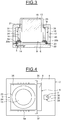
Figure 3 represents a transverse local cross section, according to III-III of the electronic device ofFigure 1 ; -
Figure 4 represents a top view of the electronic device ofFigure 1 , without a cap thereof; -
Figure 5 represents a longitudinal cross section of a variant embodiment of the electronic device ofFigure 1 ; -
Figure 6 represents a transverse local cross section, according to VI-VI of the electronic device ofFigure 5 ; -
Figure 7 represents a longitudinal cross section of a variant embodiment of the electronic device ofFigure 5 ; and -
Figure 8 represents a transverse local cross section, according to VIII-VIII of the electronic device ofFigure 7 . - According to a variant embodiment, an
electronic device 1, illustrated onFigures 1-4 , comprises a rectangular support plate (or substrate) 2, made of an insulated material, having arear face 3 and afront face 4 and including an integratednetwork 5 of electrical connections from one face to the other. For example, thesupport plate 2 is rectangular. - The
electronic device 1 comprises an electronic integratedcircuit chip 6 having arear face 7 mounted on thefront face 4 of thesupport plate 2, by means of a glue layer, and afront face 8 which includes a local optical component such as alight sensor 9. Thechip 6 is rectangular and has edges which are distant from and parallel to the edges of the support plate. - The
electronic device 1 comprises a sleeve (or barrel) 10 forming atraversing passage 11 and having arear edge 12 and afront edge 13 at the opposite ends of thetraversing passage 11. - The
sleeve 10 is mounted on thefront face 8 of thechip 6 in such a position that thelight sensor 9 of thechip 6 is facing thetraversing passage 11 and that therear edge 12 surrounds at a distance thelight sensor 9. The axis of thesleeve 10 is placed perpendicularly to thefront face 8 of thechip 6. - The
rear edge 12 of thesleeve 10 is attached to thefront face 8 of thechip 8, by means of aglue bead 14. - So, the
sleeve 10 constitutes a specific and local light guide via thetraverse passage 11. - The
sleeve 10 carries anoptical element 15 situated inside thetraversing passage 11 and facing at a distance thelight sensor 9, theoptical element 15 allowing light to pass through. Theoptical element 15 can include an optical lens and eventually a light filter. - The natural or ambient light traverses the
optical element 15 and reaches thelight sensor 9. Advantageously, thesleeve 10 and theglue bead 14 are adapted such that the natural or ambient light reaching thelight sensor 9 is issued only from the front end of thetraversing passage 11 of thesleeve 10. - The
sleeve 10 is mounted on thesupport plate 2 such that the optical axis of light sensor and the optical axis of theoptical element 15 are confused. - The
chip 6 is electrically connected to the connection network of thesupport plate 2 by means ofelectrical connection wires 6a (Figures 3 and 4 ) which connect front pads of thechip 6 and front pads of thesupport plate 2. - According to one embodiment, the front pads of the
chip 6 are situated outside the region of thefront face 8 of thechip 6 covered by thesleeve 10. - According to another embodiment shown in the drawings, the
sleeve 10 hasindentations 16 formed in therear edge 12. The front pads of thechip 6 are situated in the region of theindentations 16 and portions of thewires 6a enter inside theindentations 16. In this case, theglue bead 14 fills theindentations 16 and thewires 6a are at least partially drowned in theglue bead 14. - The
electronic device 1 comprises acap 17 which delimits achamber 18 forward thesupport plate 2, which contains thechip 6 and at least a rear portion of thesleeve 10. - The
cap 17 comprises afront wall 19 and aperipheral wall 20. - The
front wall 19 is at a distance over thesupport plate 2 and has anopening 21 which coincides with thesleeve 10 such that thepassage 11 of thesleeve 10 is opened to the outside for letting pass the natural light towards thepassage 11 of thesleeve 10. - The
peripheral wall 20 extends backwards from thefront wall 19 and towards a peripheral zone of thefront face 4 of thesupport plate 2. - The
cap 17 is attached to thesupport plate 2 by means of aglue bead 22 interposed between the peripheral zone of thefront face 4 of thesupport plate 2 and arear edge 23 of theperipheral wall 20. - The
sleeve 10 comprises arear portion 24 in thechamber 18 and afront portion 25 which traverses freely the opening 21 of thefront wall 19 of thecap 17. - Between the
rear portion 24 in thechamber 18 and thefront portion 25, thesleeve 10 has aperipheral shoulder 26 facing a zone of the rear face of thefront wall 19 surrounding the opening 21. Aglue bead 27 is interposed between theshoulder 26 and thefront wall 19. - The
rear portion 24 has a square section, the sides of which are parallel to the edge of thechip 6. Theindentations 16 being made in two opposite sides thereof. Thefront portion 25 has a cylindrical section and contains theoptical element 15. - The glue bead 22 and/or the
glue beads 27 are formed such that the natural light is prevented from reaching thelight sensor 9 other than through the front end of thetraversing passage 11 of thesleeve 10. - The
electronic device 1 comprises another electronic integratedcircuit chip 28 mounted on thefront face 4 of thesupport plate 2 at a distance from thechip 6 and inchamber 18 of thecap 17. - The
chip 28 has arear face 29 fixed to thefront face 4 of thesupport plate 2 and afront face 30 which includes a local optical component such as alight emitter 31. - The
chip 28 is connected electrically to theconnection network 5 by connection means including anelectrical connection wire 32. - The
front wall 19 of thecap 17 has anopening 33 in front of thelight emitter 31 and provided with anoptical element 34 allowing light to pass through. Theoptical element 34 can include an optical lens and eventually a light filter. - The
sleeve 10 is linked to thechip 6 and thecap 17 so as to constitute a barrier such that the light emitted by theemitter 30 do not reach thelight sensor 9 directly via thechamber 18 of thecap 17. - Advantageously, the
glue bead 14 contributes to achieve this result. - Nevertheless, this result can also be achieved by linking the
sleeve 10 to thechip 6 and thecap 17 so as to delimit achamber portion 35 of thechamber 18 in which thechip 28 is located. - For delimiting the
chamber portion 35, therear portion 24 of thesleeve 10 has aside 24a turned on the side of thechip 28 and comprises opposite projectingribs opposite sides peripheral wall 20 of thecap 17. Theribs peripheral wall 20, to thesupport plate 2 and to thefront wall 19 by means of glue leads 38 and 39 which join the glue leads 14 and 27. - Advantageously, the
opposite sides peripheral wall 20 of thecap 17 haveslots ribs - So, the
side 24a and theribs rear portion 24 of thesleeve 10, the portion of theglue bead 14 linking theside 24a to thechip 6, the portion of theglue bead 27 linking thesleeve 10 to thefront wall 19 of thecap 17 and theglue beads emitter 30 of thechip 28 to reach thelight sensor 9 of thechip 6. - The
chip 6 is programmed to command theemitter 30 of thechip 28 and to treat the signals issued from thelight sensor 9. - The
electronic device 1 can be manufactured as following. -
Chips support plate 2 and connected electrically to anelectrical connection network 5 of thesupport plate 2, as previously described. - Next, a
sleeve 10 carrying anoptical element 15 is mounted on thechip 10 and linked by means of aglue bead 14, as previously described, thesleeve 10 and in consequence theoptical element 15 relatively to thelight sensor 9 of thechip 6 being placed as desired. - Next, a
cap 17 carrying anoptical element 34 is mounted on thesupport plate 2 and linked by means ofglue beads cap 17 and in consequence theoptical element 34 relatively to theemitter 30 of thechip 28 being placed as desired regardless of the position of thesleeve 10 because of the peripheral gap between thefront portion 25 of thesleeve 10 and theopening 21 of thefront wall 19 of thecap 17. -
Figure 5 and 6 illustrate a variant embodiment of theelectronic device 1 offigures 1-4 , in which thefront face 8 of thechip 6 includes a local optical component such as alight sensor 42 which is located outside and at a distance from thesleeve 10 and on the side of thechip 28. The light emitted by theemitter 30 of thechip 28 in thechamber 18 reaches thelight sensor 42. - The
chip 6 is programmed to command theemitter 30 of thechip 28 and to treat the signals issued from thelight sensor 9 and thelight sensor 42. -
Figures 7 and 8 illustrate a variant embodiment of theelectronic device 1 offigures 5 and 6 , in which thecap 17 comprises further aninternal partition 43 which extends from thefront wall 19 and theopposite sides support plate 2 and thechip 6 and between and at a distance from thesleeve 10 and thelight sensor 42. - The
partition 43 has arear nick 44 which is traversed by thechip 6. Aglue bead 45 is interposed between therear nick 44 of thepartition 43 and thechip 6 and between thesupport plate 2 and the rear edge of the partition on each side of thechip 6. - So, the
partition 43 divides thechamber 18 into achamber portion 46 in which thesleeve 10 is located and achamber portion 47 in which thechip 28 and thelight sensor 42 are located. - The
partition 43 and theglue bead 45 contribute to prevent the light issued from thechip 28 in thechamber portion 47 from reaching thechamber portion 46 and in consequence from reaching thelight sensor 9. - In this variant embodiment, the
link ribs - According to a variant embodiment (not shown on the drawings), the
cap 17 of theelectronic device 1 ofFigures 1 to 4 can also comprise an partition equivalent to thepartition 43, traversed by thechip 6 and attached by means of theglue beads 45 or located between thechip 6 and thechip 28 and attached only to thesupport plate 2 by a glue bead. - According to a variant embodiment, the
sleeve 10 can be made so as not protrude from thefront wall 19 of thecap 17. - According to a variant embodiment, a complementary optical element (not shown on the drawings), such as a light filter, can be mounted on the
light sensor 9 of thechip 6. - According to a variant embodiment, the
connection wires 6a can be replaced, by connection elements interposed between the front face of thesupport plate 2 and the rear face of thechip 6. - The
electronic device 1 is particularly adapted to form a proximity sensor and/or an image sensor.
Claims (12)
- An electronic device, comprising:a support plate (2) having a rear face and a front face;an electronic integrated circuit chip (6) having a rear face mounted on the front face of the support plate (2) and including an optical component (9) in a front face; anda sleeve (10) forming a traversing passage (11) and having a rear edge (12) and a front edge (13) at the opposite ends of the traversing passage (11), the rear edge (12) being mounted on the front face of the chip (6), in such a position that the optical component (9) of the chip is facing the traversing passage (11) of the sleeve (10), anda cap (17) comprising a front wall (19) extending at a distance in front of the chip and a peripheral wall (20) having a rear end edge (23) mounted on the support plate (2), such as to delimit a chamber (18) in which the chip (6) is located, the front wall (19) of the cap (17) having a through passage (21) for the sleeve (10).
- A device according to the claim 1, wherein the traversing passage (11) of the sleeve (10) is provided with at least an optical element (15) allowing light to pass through.
- A device according to one of the claims 1 and 2, wherein a glue bead (14) inserted between the front face of the chip (6) and the rear edge of the sleeve (10).
- A device according to one of the preceding claims, comprising a glue bead (22) inserted between the support plate (2) and the end edge (23) of the peripheral wall (20) of the cap (17).
- A device according to anyone of the preceding claims, comprising a glue bead (27) inserted between the sleeve (10) and the front wall (19) of the cap (17), along the through passage (21) of the front wall (19) of the cap.
- A device according to anyone of the preceding claims, wherein the sleeve (10) comprises a rear portion (24) inside the chamber (18) of the cap (17) and a front portion (25) traversing the through passage (21) of the front wall (19) of the cap (10).
- A device according to anyone of the preceding claims, comprising a gap between the sleeve (10) and the through passage (21) of the cap (17).
- A device according to anyone of the preceding claims, wherein the chip (6) includes another optical component (42) in the front face, which is located outside the sleeve (10).
- A device according to anyone of the preceding claims, comprising another electronic integrated circuit chip (28) in the chamber of the cap, having a rear face mounted on the front face of the support plate (2) and including an optical component (30) in a front face, the front wall (18) of the cap (17) having a through passage (34) provided with an optical element (34) letting pass the light through and situated in front of this optical component (30).
- A device according to the claims 8 and 9, comprising projecting ribs (36, 37) connecting the sleeve and the cap (17) in the chamber of the cap (17) such as to divide the chamber of the cap into two chamber portions (18a, 18b) and wherein the other optical component (42) and the other chip (28) are located in the same chamber portion.
- A device according to the claim 8, wherein the cap (17) comprises an internal partition (43) divided the chamber of the cap into two chamber portions (46, 47), the sleeve (10) being located in one of these chamber portions and the other chip (28) being located in the other chamber portion.
- A device according to the claims 8 and 9, wherein the cap (17) comprises an internal partition (43) divided the chamber of the cap into two chamber portions (46, 47), the sleeve (10) being located in one of these chamber portions and the other chip (28) and the other optical component (42) being located in the other chamber portion.
Applications Claiming Priority (1)
| Application Number | Priority Date | Filing Date | Title |
|---|---|---|---|
| FR1859451 | 2018-10-11 |
Publications (1)
| Publication Number | Publication Date |
|---|---|
| EP3637466A1 true EP3637466A1 (en) | 2020-04-15 |
Family
ID=65494344
Family Applications (1)
| Application Number | Title | Priority Date | Filing Date |
|---|---|---|---|
| EP19200004.0A Pending EP3637466A1 (en) | 2018-10-11 | 2019-09-27 | Electronic device comprising a chip having an optical sensor |
Country Status (3)
| Country | Link |
|---|---|
| US (1) | US11127874B2 (en) |
| EP (1) | EP3637466A1 (en) |
| CN (2) | CN211320099U (en) |
Families Citing this family (2)
| Publication number | Priority date | Publication date | Assignee | Title |
|---|---|---|---|---|
| US20180315894A1 (en) * | 2017-04-26 | 2018-11-01 | Advanced Semiconductor Engineering, Inc. | Semiconductor device package and a method of manufacturing the same |
| EP3637466A1 (en) * | 2018-10-11 | 2020-04-15 | STMicroelectronics (Research & Development) Limited | Electronic device comprising a chip having an optical sensor |
Citations (5)
| Publication number | Priority date | Publication date | Assignee | Title |
|---|---|---|---|---|
| US20040217454A1 (en) | 2001-05-18 | 2004-11-04 | Remi Brechignac | Optical semiconductor package with incorporated lens and shielding |
| US20070228558A1 (en) | 2006-03-29 | 2007-10-04 | Stmicroelectronics S.A. | Semiconductor packaging unit with sliding cage |
| US20070272827A1 (en) * | 2005-04-27 | 2007-11-29 | Amkor Technology, Inc. | Image sensor package having mount holder attached to image sensor die |
| US20090201414A1 (en) * | 2008-02-13 | 2009-08-13 | Sharp Kabushiki Kaisha | Solid Image capture device and electronic device incorporating same |
| US20180058920A1 (en) * | 2016-08-26 | 2018-03-01 | Stmicroelectronics (Grenoble 2) Sas | Electronic housing including a grooved cover |
Family Cites Families (11)
| Publication number | Priority date | Publication date | Assignee | Title |
|---|---|---|---|---|
| TW554497B (en) * | 2002-07-03 | 2003-09-21 | Pixart Imaging Inc | Packaging method of optical mechanism and the optical mechanism |
| FR2860644B1 (en) * | 2003-10-06 | 2006-03-03 | St Microelectronics Sa | COMPONENT, PLATE AND SEMICONDUCTOR HOUSING WITH OPTICAL SENSOR |
| DE102006013164A1 (en) * | 2006-03-22 | 2007-09-27 | Robert Bosch Gmbh | Method for mounting a camera module and camera module |
| KR101711007B1 (en) * | 2010-04-29 | 2017-03-02 | 삼성전자주식회사 | Image sensor module having image sensor package |
| JP6088169B2 (en) * | 2011-08-26 | 2017-03-01 | アイリスオーヤマ株式会社 | LED lamp |
| US20130175650A1 (en) * | 2012-01-05 | 2013-07-11 | Apple Inc | Cover for image sensor assembly with light absorbing layer |
| US9608033B2 (en) * | 2014-05-12 | 2017-03-28 | Canon Kabushiki Kaisha | Solid-state image sensor, method of manufacturing the same, and camera |
| US10197890B2 (en) * | 2016-02-18 | 2019-02-05 | Ningbo Sunny Opotech Co., Ltd. | Array imaging module and molded photosensitive assembly, circuit board assembly and manufacturing methods thereof for electronic device |
| CN108243297A (en) * | 2016-12-23 | 2018-07-03 | 宁波舜宇光电信息有限公司 | Camera module and its circuit board assemblies and manufacturing method and the electronic equipment with camera module |
| FR3069406A1 (en) * | 2017-07-18 | 2019-01-25 | Stmicroelectronics (Grenoble 2) Sas | ELECTRONIC HOUSING AND METHOD OF MANUFACTURE |
| EP3637466A1 (en) * | 2018-10-11 | 2020-04-15 | STMicroelectronics (Research & Development) Limited | Electronic device comprising a chip having an optical sensor |
-
2019
- 2019-09-27 EP EP19200004.0A patent/EP3637466A1/en active Pending
- 2019-10-07 US US16/594,792 patent/US11127874B2/en active Active
- 2019-10-10 CN CN201921687255.4U patent/CN211320099U/en active Active
- 2019-10-10 CN CN201910959496.8A patent/CN111048538A/en active Pending
Patent Citations (5)
| Publication number | Priority date | Publication date | Assignee | Title |
|---|---|---|---|---|
| US20040217454A1 (en) | 2001-05-18 | 2004-11-04 | Remi Brechignac | Optical semiconductor package with incorporated lens and shielding |
| US20070272827A1 (en) * | 2005-04-27 | 2007-11-29 | Amkor Technology, Inc. | Image sensor package having mount holder attached to image sensor die |
| US20070228558A1 (en) | 2006-03-29 | 2007-10-04 | Stmicroelectronics S.A. | Semiconductor packaging unit with sliding cage |
| US20090201414A1 (en) * | 2008-02-13 | 2009-08-13 | Sharp Kabushiki Kaisha | Solid Image capture device and electronic device incorporating same |
| US20180058920A1 (en) * | 2016-08-26 | 2018-03-01 | Stmicroelectronics (Grenoble 2) Sas | Electronic housing including a grooved cover |
Also Published As
| Publication number | Publication date |
|---|---|
| CN211320099U (en) | 2020-08-21 |
| CN111048538A (en) | 2020-04-21 |
| US20200119219A1 (en) | 2020-04-16 |
| US11127874B2 (en) | 2021-09-21 |
Similar Documents
| Publication | Publication Date | Title |
|---|---|---|
| US7327005B2 (en) | Optical semiconductor package with incorporated lens and shielding | |
| US5350943A (en) | Semiconductor assembly, in particular a remote control reception module | |
| KR102213027B1 (en) | Camera assembly with shielded imager circuit | |
| US10651101B2 (en) | Electronic package with a local slot forming an air-vent | |
| JP3819893B2 (en) | Double-cap bidirectional optical communication module | |
| US20180007244A1 (en) | Photosensitive Assembly and Camera Module and Manufacturing Method Thereof | |
| US11127874B2 (en) | Electronic device comprising a chip provided with an optical sensor | |
| EP2657739A1 (en) | Optical connector | |
| US10480994B2 (en) | Electronic housing including a grooved cover | |
| DE19610388A1 (en) | Ignition device e.g. for discharge lamp of motor vehicle | |
| WO2008083672A2 (en) | Housing for an optoelectronic component and arrangement of an optoelectronic component in a housing | |
| DE102016202563A1 (en) | RETROFIT LAMP AND VEHICLE HEADLAMP WITH RETROFIT LAMP | |
| DE102017101945B4 (en) | Measurement setup with an optical transmitter and an optical receiver | |
| CN112841153A (en) | Insect catching device and counting method thereof | |
| US20150035396A1 (en) | Motor provided with terminal block | |
| US6583401B2 (en) | Optoelectronic component with a conductor strip element | |
| CN109979886B (en) | Covers for electronic circuit packages | |
| KR20230044947A (en) | Lidar Sensor that cancelling noise by shielding EMI and light-leakage | |
| US7665873B2 (en) | Headlamp for vehicles | |
| US20080102657A1 (en) | Device for electrical contacting | |
| CN209087834U (en) | Encapsulation lids and electronic packages for electronic packages | |
| JP2015211310A (en) | Filter element built-in connector | |
| EP3745022B1 (en) | Vehicle luminaire and vehicle lamp | |
| EP3201650B1 (en) | Window cap for the housing of a scanning optoelectronic measuring device and housing with same | |
| WO2012002386A1 (en) | Electronic component |
Legal Events
| Date | Code | Title | Description |
|---|---|---|---|
| PUAI | Public reference made under article 153(3) epc to a published international application that has entered the european phase |
Free format text: ORIGINAL CODE: 0009012 |
|
| STAA | Information on the status of an ep patent application or granted ep patent |
Free format text: STATUS: REQUEST FOR EXAMINATION WAS MADE |
|
| 17P | Request for examination filed |
Effective date: 20190927 |
|
| AK | Designated contracting states |
Kind code of ref document: A1 Designated state(s): AL AT BE BG CH CY CZ DE DK EE ES FI FR GB GR HR HU IE IS IT LI LT LU LV MC MK MT NL NO PL PT RO RS SE SI SK SM TR |
|
| AX | Request for extension of the european patent |
Extension state: BA ME |