EP3637263A1 - Vehicle control device, and vehicle control simulation device - Google Patents
Vehicle control device, and vehicle control simulation device Download PDFInfo
- Publication number
- EP3637263A1 EP3637263A1 EP18828170.3A EP18828170A EP3637263A1 EP 3637263 A1 EP3637263 A1 EP 3637263A1 EP 18828170 A EP18828170 A EP 18828170A EP 3637263 A1 EP3637263 A1 EP 3637263A1
- Authority
- EP
- European Patent Office
- Prior art keywords
- information
- arithmetic
- control model
- delay
- control
- Prior art date
- Legal status (The legal status is an assumption and is not a legal conclusion. Google has not performed a legal analysis and makes no representation as to the accuracy of the status listed.)
- Pending
Links
Images



Classifications
-
- G—PHYSICS
- G06—COMPUTING OR CALCULATING; COUNTING
- G06F—ELECTRIC DIGITAL DATA PROCESSING
- G06F8/00—Arrangements for software engineering
- G06F8/30—Creation or generation of source code
- G06F8/35—Creation or generation of source code model driven
-
- B—PERFORMING OPERATIONS; TRANSPORTING
- B60—VEHICLES IN GENERAL
- B60W—CONJOINT CONTROL OF VEHICLE SUB-UNITS OF DIFFERENT TYPE OR DIFFERENT FUNCTION; CONTROL SYSTEMS SPECIALLY ADAPTED FOR HYBRID VEHICLES; ROAD VEHICLE DRIVE CONTROL SYSTEMS FOR PURPOSES NOT RELATED TO THE CONTROL OF A PARTICULAR SUB-UNIT
- B60W50/00—Details of control systems for road vehicle drive control not related to the control of a particular sub-unit, e.g. process diagnostic or vehicle driver interfaces
- B60W50/04—Monitoring the functioning of the control system
-
- G—PHYSICS
- G05—CONTROLLING; REGULATING
- G05B—CONTROL OR REGULATING SYSTEMS IN GENERAL; FUNCTIONAL ELEMENTS OF SUCH SYSTEMS; MONITORING OR TESTING ARRANGEMENTS FOR SUCH SYSTEMS OR ELEMENTS
- G05B17/00—Systems involving the use of models or simulators of said systems
- G05B17/02—Systems involving the use of models or simulators of said systems electric
-
- G—PHYSICS
- G06—COMPUTING OR CALCULATING; COUNTING
- G06F—ELECTRIC DIGITAL DATA PROCESSING
- G06F11/00—Error detection; Error correction; Monitoring
- G06F11/30—Monitoring
- G06F11/34—Recording or statistical evaluation of computer activity, e.g. of down time, of input/output operation ; Recording or statistical evaluation of user activity, e.g. usability assessment
- G06F11/3404—Recording or statistical evaluation of computer activity, e.g. of down time, of input/output operation ; Recording or statistical evaluation of user activity, e.g. usability assessment for parallel or distributed programming
-
- G—PHYSICS
- G06—COMPUTING OR CALCULATING; COUNTING
- G06F—ELECTRIC DIGITAL DATA PROCESSING
- G06F11/00—Error detection; Error correction; Monitoring
- G06F11/30—Monitoring
- G06F11/34—Recording or statistical evaluation of computer activity, e.g. of down time, of input/output operation ; Recording or statistical evaluation of user activity, e.g. usability assessment
- G06F11/3409—Recording or statistical evaluation of computer activity, e.g. of down time, of input/output operation ; Recording or statistical evaluation of user activity, e.g. usability assessment for performance assessment
- G06F11/3419—Recording or statistical evaluation of computer activity, e.g. of down time, of input/output operation ; Recording or statistical evaluation of user activity, e.g. usability assessment for performance assessment by assessing time
-
- G—PHYSICS
- G06—COMPUTING OR CALCULATING; COUNTING
- G06F—ELECTRIC DIGITAL DATA PROCESSING
- G06F11/00—Error detection; Error correction; Monitoring
- G06F11/30—Monitoring
- G06F11/34—Recording or statistical evaluation of computer activity, e.g. of down time, of input/output operation ; Recording or statistical evaluation of user activity, e.g. usability assessment
- G06F11/3447—Performance evaluation by modeling
-
- G—PHYSICS
- G06—COMPUTING OR CALCULATING; COUNTING
- G06F—ELECTRIC DIGITAL DATA PROCESSING
- G06F11/00—Error detection; Error correction; Monitoring
- G06F11/30—Monitoring
- G06F11/34—Recording or statistical evaluation of computer activity, e.g. of down time, of input/output operation ; Recording or statistical evaluation of user activity, e.g. usability assessment
- G06F11/3457—Performance evaluation by simulation
-
- G—PHYSICS
- G06—COMPUTING OR CALCULATING; COUNTING
- G06F—ELECTRIC DIGITAL DATA PROCESSING
- G06F30/00—Computer-aided design [CAD]
- G06F30/10—Geometric CAD
- G06F30/15—Vehicle, aircraft or watercraft design
-
- G—PHYSICS
- G06—COMPUTING OR CALCULATING; COUNTING
- G06F—ELECTRIC DIGITAL DATA PROCESSING
- G06F30/00—Computer-aided design [CAD]
- G06F30/30—Circuit design
- G06F30/32—Circuit design at the digital level
- G06F30/33—Design verification, e.g. functional simulation or model checking
- G06F30/3308—Design verification, e.g. functional simulation or model checking using simulation
-
- G—PHYSICS
- G06—COMPUTING OR CALCULATING; COUNTING
- G06F—ELECTRIC DIGITAL DATA PROCESSING
- G06F30/00—Computer-aided design [CAD]
- G06F30/30—Circuit design
- G06F30/32—Circuit design at the digital level
- G06F30/33—Design verification, e.g. functional simulation or model checking
- G06F30/3308—Design verification, e.g. functional simulation or model checking using simulation
- G06F30/3312—Timing analysis
-
- H—ELECTRICITY
- H04—ELECTRIC COMMUNICATION TECHNIQUE
- H04L—TRANSMISSION OF DIGITAL INFORMATION, e.g. TELEGRAPHIC COMMUNICATION
- H04L67/00—Network arrangements or protocols for supporting network services or applications
- H04L67/01—Protocols
- H04L67/12—Protocols specially adapted for proprietary or special-purpose networking environments, e.g. medical networks, sensor networks, networks in vehicles or remote metering networks
-
- G—PHYSICS
- G06—COMPUTING OR CALCULATING; COUNTING
- G06F—ELECTRIC DIGITAL DATA PROCESSING
- G06F2115/00—Details relating to the type of the circuit
- G06F2115/10—Processors
Definitions
- the present invention relates to a vehicle control device and a vehicle control simulation device.
- An embedded control device that controls a control target with so-called embedded software, is used in the technical field of automobiles, elevators, construction machines, and the like.
- embedded software enables achievement of more flexible and advanced control than a conventional system with a mechanical mechanism or an electric circuit.
- Such an embedded control device for example, a control device in a vehicle controls an engine and brakes with a plurality of electronic control units (ECUs), to control the entirety of the vehicle.
- ECUs electronice control units
- One ECU such as an ECU for engine control, achieves intricate control with a plurality of built-in processor cores.
- An object of the present invention is to provide a vehicle control device and a vehicle control simulation device that enable, even for parallel processing with a plurality of arithmetic devices, approximation in act between at verification of simulation operation on a model base and at verification of operation on an actual vehicle.
- control model information for control of a system includes hardware information for operation of a control model; arithmetic-device allocation information as to which arithmetic device in the hardware is allocated to perform arithmetic processing to a control program in the control model; delay time information regarding a case where the control model operates on the hardware; and a delay-time adding unit configured to create delay-inclusive control model information in which the delay time information is inserted in the control model, based on at least either the arithmetic-device allocation information or the hardware information.
- the present embodiment relates to an embedded system including a computer system embedded for achievement of a specific function of a product requiring electronic control, such as household equipment, industrial equipment, or medical equipment.
- the present embodiment relates to a vehicle control device and a vehicle control simulation device each that control a system with a plurality of arithmetic devices, for example, a system in which required functions are various, for transport equipment, such as automobiles, railways, and elevators, or a large-scale system having a combination of a plurality of pieces of hardware and a plurality of pieces of software.
- FIG. 1 is a system block diagram of a vehicle control simulation device according to the embodiment of the present invention.
- the vehicle control simulation device 1 includes a control model 101, an HW configuration 102, arithmetic-device allocation 103, delay time 104, and a delay-time adding unit 105.
- the delay-time adding unit 105 generates a delay-inclusive control model 106, on the basis of the control model 101, the HW configuration 102, the arithmetic-device allocation 103, and the delay time 104.
- a waveform chart 108 indicating a simulation result based on the delay-inclusive control model 106 after application of the present embodiment indicates that the waveform has changed due to the influence of the delay time 104.
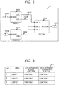
- FIG. 2 is a model diagram of the control model according to the embodiment of the present invention.
- the control model 101 includes input ports 10101 and 10102, an output port 10106, and functional blocks 10103, 10104, and 10105. Transmission and reception of label information 1 and label information 2 are indicated between the functional block 10103 and the functional block 10105 through wiring lines 10107 and 10108 indicating data dependent relationship. Similarly, transmission and reception of label information 3 are performed between the functional block 10104 and the functional block 10105 through a wiring line 10109 indicating data dependent relationship.
- the functional block 10103 inputs sensor 1 information from the input port 10101, and outputs the label 1 information and the label 2 information to the functional block 10105.
- the functional block 10104 inputs sensor 2 information from the input port 10102, and outputs the label 3 information to the functional block 10105. Then, the functional block 10105 inputs the label 1 information and the label 2 information output from the functional block 10103 and the label 3 information output from the functional block 10104, and outputs actuator 1 information to the output port 10106.
- FIG. 3 is a data table of the control model according to the embodiment of the present invention.
- the data table 1011 of the control model includes information regarding ID, label, data dependent source function, and data dependent destination function. Specifically, the data table 1011 indicates the data dependent source function and the data dependent destination function of the label 1, label 2, and label 3 information to be transmitted and received between the functional blocks 10103, 10104, and 10105 indicated in the control model 101.
- the data dependent source function indicates a function 1 that is the functional block 10103 in the control model 101
- the data dependent destination function indicates a function 3 that is the functional block 10105 in the control model 101.
- FIG. 4 is a block diagram of the HW configuration according to the embodiment of the present invention.
- the HW configuration 102 indicates an HW configuration for arithmetic processing of control software written in the control model 101.
- the HW configuration 102 includes an ECU 10201, an actuator 10202, sensors 10203 and 10204, and a bus 10205.
- the ECU 10201 includes arithmetic devices 1020101, 1020102, and 1020103, and a memory 10201.
- FIG. 5 is a data table of the HW configuration according to the embodiment of the present invention.
- the data table 1021 of the HW configuration includes data dependent source, data dependent destination, and delay determination information.
- the data table 1021 includes the delay determination information that is criterial for determination of whether delay occurs in data communication between the arithmetic devices 1020101, 1020102, and 1020103.
- the delay determination information that is criterial for determination of whether delay occurs in data communication between the arithmetic devices 1020101, 1020102, and 1020103.
- the arithmetic device 1020101 is an arithmetic device 1 indicated as the data dependent source
- the arithmetic device 1020102 is an arithmetic device 2 indicated as the data dependent destination
- the data table 1021 indicates that no delay time occurs because the delay determination indicates no delay.
- the data table 1021 indicates that delay time occurs because the delay determination indicates delay.
- FIG. 6 is a data table of the arithmetic-device allocation according to the embodiment of the present invention.
- the data table 103 of the arithmetic-device allocation includes function and allocation information. Specifically, the data table 103 indicates which arithmetic device indicated in the HW configuration 102 performs arithmetic processing to each function indicated in the control model 101. For example, the data table 103 indicates that the functional block 10103 indicated as the function 1 in the control model 101 is to be subjected to arithmetic processing by the arithmetic device 1020101 indicated as the arithmetic device 1 in the HW configuration 102.
- the data table 103 indicates that the functional block 10104 indicated as the function 2 in the control model 102 is to be subjected to arithmetic processing by the arithmetic device 1020102 indicated as the arithmetic device 2 in the HW configuration 102.
- FIG. 7 is a data table of the delay time according to the embodiment of the present invention.
- the data table 104 of the delay time includes function and delay time information. Specifically, the data table 104 indicates the processing time necessary in a case where each function indicated in the control model 101 is subjected to the arithmetic processing by the arithmetic device in the HW configuration 102. For example, in a case where the desired block 10103 indicated as the function 1 in the control model 101 is processed by the arithmetic device in the HW configuration 102, the data table 104 indicates that the processing time is 2.20 ⁇ s.
- FIG. 8 is a flowchart of the act of the delay-time adding unit according to the embodiment of the present invention.
- the delay-time adding unit 105 generates the delay-inclusive control model 106 in which the delay information 104 is added to the control model 101, on the basis of the HW configuration 102, the arithmetic-device allocation 103, and the delay time 104 information.
- the processing starts from step S10501 as the act of the delay-time adding unit 105.
- step S10502 label information in the control model 1011 is acquired and then the data dependent source function and the data dependent destination function related to the label are specified.
- the arithmetic-device allocation 103 is acquired, and then it is specified to which arithmetic devices the data dependent source function and the data dependent destination function related to the label in the control model information are allocated.
- the HW configuration 1021 information is acquired, and then it is specified whether the delay determination indicates delay or no delay, from a combination of the arithmetic devices to which the data dependent source function and the data dependent destination function related to the label in the control model information are allocated.
- step S10507 the delay time information from the delay time 104 is acquired, and then the delay time necessary for arithmetic processing of the data dependent source function related to the label, is specified.
- step S10508 a delay block based on the delay time 104 information is inserted in the wiring portion related to the label in the delay model 101.
- step S10509 it is determined whether the determination at step S10505 has been performed to all the labels in the control model 1011. For YES, the processing proceeds to step S1020110, to finish.
- step S10507 the data dependent source function and the data dependent destination function related to the next label in the control model 1011, are specified.
- FIG. 9 is a model diagram of the delay-inclusive control model according to the embodiment of the present invention.
- the delay-inclusive control model 1011 results from addition of the delay time 104 to the control model 101 by the delay-time adding unit 105.
- the present embodiment indicates the result of addition of the delay time information to wiring lines 10117 and 10118 related to the label 1 and the label 2 to be subjected to data transmission and reception between a functional block 10113 and a functional block 10115.
- FIG. 10 illustrates waveform charts of simulation results of the control model and the delay-inclusive control model according to the embodiment of the present invention.
- the waveform chart 108 indicating the simulation result of the delay-inclusive control model 1011 clearly indicates that the waveform has changed because of the insertion of the delay blocks, in comparison to the waveform chart 107 indicating the simulation result of the control model 101.
- This arrangement enables taking account of the influence of the synchronous processing time between pieces of arithmetic processing due to parallel processing with a plurality of arithmetic devices or the influence of delay time due to data communication in arithmetic processing time, having not been considered in the existing model-based development. Thus, disagreement is inhibited from occurring between at verification of simulation operation on a model base and at verification of operation on an actual vehicle, so that the performance estimated at design can be secured.
Landscapes
- Engineering & Computer Science (AREA)
- Theoretical Computer Science (AREA)
- Physics & Mathematics (AREA)
- General Engineering & Computer Science (AREA)
- General Physics & Mathematics (AREA)
- Computer Hardware Design (AREA)
- Automation & Control Theory (AREA)
- Geometry (AREA)
- Quality & Reliability (AREA)
- Evolutionary Computation (AREA)
- Software Systems (AREA)
- Transportation (AREA)
- Mechanical Engineering (AREA)
- Computer Networks & Wireless Communication (AREA)
- Human Computer Interaction (AREA)
- Health & Medical Sciences (AREA)
- General Health & Medical Sciences (AREA)
- Computing Systems (AREA)
- Signal Processing (AREA)
- Medical Informatics (AREA)
- Pure & Applied Mathematics (AREA)
- Mathematical Optimization (AREA)
- Mathematical Analysis (AREA)
- Computational Mathematics (AREA)
- Life Sciences & Earth Sciences (AREA)
- Bioinformatics & Cheminformatics (AREA)
- Bioinformatics & Computational Biology (AREA)
- Evolutionary Biology (AREA)
- Aviation & Aerospace Engineering (AREA)
- Debugging And Monitoring (AREA)
- Stored Programmes (AREA)
- Feedback Control In General (AREA)
Abstract
Description
- The present invention relates to a vehicle control device and a vehicle control simulation device.
- An embedded control device that controls a control target with so-called embedded software, is used in the technical field of automobiles, elevators, construction machines, and the like. Advantageously, such embedded software enables achievement of more flexible and advanced control than a conventional system with a mechanical mechanism or an electric circuit.
- Such an embedded control device, for example, a control device in a vehicle controls an engine and brakes with a plurality of electronic control units (ECUs), to control the entirety of the vehicle. One ECU, such as an ECU for engine control, achieves intricate control with a plurality of built-in processor cores.
- However, along with the complication of control, the development scale of embedded software increases. Thus, the man-hour necessary for design and verification of embedded software continuously increases. Regarding this problem, for improvement in the efficiency of development of a vehicle control device, known is the technology of embedded software development on a model base enabling design and verification with simulation without an actual ECU or engine. For example,
PTL 1 discloses such technology. - Meanwhile, regarding an ECU that performs arithmetic processing to embedded software large in scale, for increase of a program amount arithmetically processable per unit of time, a speed-up technique in which parallel processing is performed with a plurality of arithmetic devices, such as ECUs or processor cores, has been introduced. For a control device in a vehicle, known is the technology of parallelization in which a plurality of arithmetic devices efficiently processes a program for vehicle control. For example,
PTL 2 discloses such technology. -
- PTL 1: Japanese Patent Application No.
H9-162169 - PTL 2: Japanese Patent Application No.
2015-501402 - However, in the existing technology of software development with a model base, the influence of parallel processing with a plurality of arithmetic devices has not been considered. Thus, there is a large gap between embedded software designed on the model base and embedded software for parallel operation, implemented on ECUs, so that discrepancy is large between the embedded software designed on the model base and the actual-equipment performance, resulting in a problem.
- More specifically, in the existing model-based development, the influence of synchronous processing time between pieces of arithmetic processing due to parallel processing with a plurality of arithmetic devices or the influence of delay time due to data communication between pieces of arithmetic processing have not been considered. Thus, disagreement occurs between at verification of simulation operation on the model base and at verification of operation on the actual vehicle, so that the performance estimated at design is not fulfilled, resulting in a problem.
- The present invention has been made in consideration of the problem. An object of the present invention is to provide a vehicle control device and a vehicle control simulation device that enable, even for parallel processing with a plurality of arithmetic devices, approximation in act between at verification of simulation operation on a model base and at verification of operation on an actual vehicle.
- In order to achieve the object, according to the present invention, provided are: control model information for control of a system; hardware information for operation of a control model; arithmetic-device allocation information as to which arithmetic device in the hardware is allocated to perform arithmetic processing to a control program in the control model; delay time information regarding a case where the control model operates on the hardware; and a delay-time adding unit configured to create delay-inclusive control model information in which the delay time information is inserted in the control model, based on at least either the arithmetic-device allocation information or the hardware information.
- According to the present invention, even in a case where parallel processing is performed with a plurality of arithmetic devices, an approximation can be made in act between simulation operation on a model base and operation on an actual vehicle. Thus, the man-hour in development can be reduced.
-
- [
FIG. 1] FIG. 1 is a system block diagram of a vehicle control simulation device according to an embodiment of the present invention. - [
FIG. 2] FIG. 2 is a model diagram of a control model according to the embodiment of the present invention. - [
FIG. 3] FIG. 3 is a data table of the control model according to the embodiment of the present invention. - [
FIG. 4] FIG. 4 is a block diagram of an HW configuration according to the embodiment of the present invention. - [
FIG. 5] FIG. 5 is a data table of the HW configuration according to the embodiment of the present invention. - [
FIG. 6] FIG. 6 is a data table of arithmetic-device allocation according to the embodiment of the present invention. - [
FIG. 7] FIG. 7 is a data table of delay time according to the embodiment of the present invention. - [
FIG. 8] FIG. 8 is a flowchart of the act of a delay-time adding unit according to the embodiment of the present invention. - [
FIG. 9] FIG. 9 is a model diagram of a delay-inclusive control model according to the embodiment of the present invention. - [
FIG. 10] FIG. 10 illustrates waveform charts of simulation results of the control model and the delay-inclusive control model according to the embodiment of the present invention. - The present embodiment relates to an embedded system including a computer system embedded for achievement of a specific function of a product requiring electronic control, such as household equipment, industrial equipment, or medical equipment. Particularly, the present embodiment relates to a vehicle control device and a vehicle control simulation device each that control a system with a plurality of arithmetic devices, for example, a system in which required functions are various, for transport equipment, such as automobiles, railways, and elevators, or a large-scale system having a combination of a plurality of pieces of hardware and a plurality of pieces of software.
- An embodiment of the present invention will be described below with reference to the drawings. Note that, for convenience, one ECU is a target in the embodiment. However, the effect of the present invention is not limited to the inside of the ECU.
-
FIG. 1 is a system block diagram of a vehicle control simulation device according to the embodiment of the present invention. The vehiclecontrol simulation device 1 includes acontrol model 101, anHW configuration 102, arithmetic-device allocation 103,delay time 104, and a delay-time adding unit 105. The delay-time adding unit 105 generates a delay-inclusive control model 106, on the basis of thecontrol model 101, theHW configuration 102, the arithmetic-device allocation 103, and thedelay time 104. - Here, in comparison to a
waveform chart 107 indicating a simulation result based on thecontrol model 101 before application of the present embodiment, awaveform chart 108 indicating a simulation result based on the delay-inclusive control model 106 after application of the present embodiment, indicates that the waveform has changed due to the influence of thedelay time 104. -
FIG. 2 is a model diagram of the control model according to the embodiment of the present invention. Thecontrol model 101 includesinput ports output port 10106, andfunctional blocks label information 1 andlabel information 2 are indicated between thefunctional block 10103 and thefunctional block 10105 throughwiring lines label information 3 are performed between thefunctional block 10104 and thefunctional block 10105 through awiring line 10109 indicating data dependent relationship. - The
functional block 10103inputs sensor 1 information from theinput port 10101, and outputs thelabel 1 information and thelabel 2 information to thefunctional block 10105. Thefunctional block 10104inputs sensor 2 information from theinput port 10102, and outputs thelabel 3 information to thefunctional block 10105. Then, thefunctional block 10105 inputs thelabel 1 information and thelabel 2 information output from thefunctional block 10103 and thelabel 3 information output from thefunctional block 10104, andoutputs actuator 1 information to theoutput port 10106. -
FIG. 3 is a data table of the control model according to the embodiment of the present invention. The data table 1011 of the control model includes information regarding ID, label, data dependent source function, and data dependent destination function. Specifically, the data table 1011 indicates the data dependent source function and the data dependent destination function of thelabel 1,label 2, andlabel 3 information to be transmitted and received between thefunctional blocks control model 101. For example, for thelabel 1 withID 1, the data dependent source function indicates afunction 1 that is thefunctional block 10103 in thecontrol model 101, and the data dependent destination function indicates afunction 3 that is thefunctional block 10105 in thecontrol model 101. -
FIG. 4 is a block diagram of the HW configuration according to the embodiment of the present invention. TheHW configuration 102 indicates an HW configuration for arithmetic processing of control software written in thecontrol model 101. TheHW configuration 102 includes anECU 10201, anactuator 10202,sensors bus 10205. TheECU 10201 includesarithmetic devices memory 10201. -
FIG. 5 is a data table of the HW configuration according to the embodiment of the present invention. The data table 1021 of the HW configuration includes data dependent source, data dependent destination, and delay determination information. - Specifically, the data table 1021 includes the delay determination information that is criterial for determination of whether delay occurs in data communication between the
arithmetic devices arithmetic device 1020101 is anarithmetic device 1 indicated as the data dependent source and thearithmetic device 1020102 is anarithmetic device 2 indicated as the data dependent destination, the data table 1021 indicates that no delay time occurs because the delay determination indicates no delay. Meanwhile, in a case where thearithmetic device 1020101 is thearithmetic device 1 indicated as the data dependent destination and thearithmetic device 1020103 is an arithmetic device n indicated as the data dependent destination, the data table 1021 indicates that delay time occurs because the delay determination indicates delay. -
FIG. 6 is a data table of the arithmetic-device allocation according to the embodiment of the present invention. - The data table 103 of the arithmetic-device allocation includes function and allocation information. Specifically, the data table 103 indicates which arithmetic device indicated in the
HW configuration 102 performs arithmetic processing to each function indicated in thecontrol model 101. For example, the data table 103 indicates that thefunctional block 10103 indicated as thefunction 1 in thecontrol model 101 is to be subjected to arithmetic processing by thearithmetic device 1020101 indicated as thearithmetic device 1 in theHW configuration 102. Similarly, the data table 103 indicates that thefunctional block 10104 indicated as thefunction 2 in thecontrol model 102 is to be subjected to arithmetic processing by thearithmetic device 1020102 indicated as thearithmetic device 2 in theHW configuration 102. -
FIG. 7 is a data table of the delay time according to the embodiment of the present invention. The data table 104 of the delay time includes function and delay time information. Specifically, the data table 104 indicates the processing time necessary in a case where each function indicated in thecontrol model 101 is subjected to the arithmetic processing by the arithmetic device in theHW configuration 102. For example, in a case where the desiredblock 10103 indicated as thefunction 1 in thecontrol model 101 is processed by the arithmetic device in theHW configuration 102, the data table 104 indicates that the processing time is 2.20 µs. -
FIG. 8 is a flowchart of the act of the delay-time adding unit according to the embodiment of the present invention. The delay-time adding unit 105 generates the delay-inclusive control model 106 in which thedelay information 104 is added to thecontrol model 101, on the basis of theHW configuration 102, the arithmetic-device allocation 103, and thedelay time 104 information. As indicated in the flowchart, the processing starts from step S10501 as the act of the delay-time adding unit 105. At step S10502, label information in thecontrol model 1011 is acquired and then the data dependent source function and the data dependent destination function related to the label are specified. At step S10503, the arithmetic-device allocation 103 is acquired, and then it is specified to which arithmetic devices the data dependent source function and the data dependent destination function related to the label in the control model information are allocated. At step 10504, theHW configuration 1021 information is acquired, and then it is specified whether the delay determination indicates delay or no delay, from a combination of the arithmetic devices to which the data dependent source function and the data dependent destination function related to the label in the control model information are allocated. At step S10505, it is determined whether the delay determination indicates delay or no delay, from the combination of the arithmetic devices to which the data dependent source function and the data dependent destination function related to the label are allocated. For YES, the processing proceeds to step S10506. For NO, the processing proceeds to step S10507. At step S10506, the delay time information from thedelay time 104 is acquired, and then the delay time necessary for arithmetic processing of the data dependent source function related to the label, is specified. At step S10508, a delay block based on thedelay time 104 information is inserted in the wiring portion related to the label in thedelay model 101. At step S10509, it is determined whether the determination at step S10505 has been performed to all the labels in thecontrol model 1011. For YES, the processing proceeds to step S1020110, to finish. - For NO, the processing proceeds to step S10507, to continue. At step S10507, the data dependent source function and the data dependent destination function related to the next label in the
control model 1011, are specified. -
FIG. 9 is a model diagram of the delay-inclusive control model according to the embodiment of the present invention. The delay-inclusive control model 1011 results from addition of thedelay time 104 to thecontrol model 101 by the delay-time adding unit 105. The present embodiment indicates the result of addition of the delay time information towiring lines label 1 and thelabel 2 to be subjected to data transmission and reception between afunctional block 10113 and afunctional block 10115. -
FIG. 10 illustrates waveform charts of simulation results of the control model and the delay-inclusive control model according to the embodiment of the present invention. Thewaveform chart 108 indicating the simulation result of the delay-inclusive control model 1011, clearly indicates that the waveform has changed because of the insertion of the delay blocks, in comparison to thewaveform chart 107 indicating the simulation result of thecontrol model 101. - This arrangement enables taking account of the influence of the synchronous processing time between pieces of arithmetic processing due to parallel processing with a plurality of arithmetic devices or the influence of delay time due to data communication in arithmetic processing time, having not been considered in the existing model-based development. Thus, disagreement is inhibited from occurring between at verification of simulation operation on a model base and at verification of operation on an actual vehicle, so that the performance estimated at design can be secured.
-
- 1
- vehicle control simulation device
- 101
- control model
- 102
- HW configuration
- 103
- arithmetic-device allocation
- 104
- delay time
- 105
- delay-time adding unit
- 106
- delay-inclusive control model
- 107
-
waveform chart 1 - 108
-
waveform chart 2
Claims (7)
- A vehicle control device comprising:control model information for control of a system;hardware information for operation of a control model;arithmetic-device allocation information as to which arithmetic device in the hardware is allocated to perform arithmetic processing to a control program in the control model;delay time information regarding a case where the control model operates on the hardware; anda delay-time adding unit configured to create delay-inclusive control model information in which the delay time information is inserted in the control model, based on at least either the arithmetic-device allocation information or the hardware information.
- The vehicle control device according to claim 1, wherein the delay-time adding unit inserts the delay time information, among combinations of functional blocks in the control model, into a combination of functional blocks in which the respective allocated arithmetic devices are different, based on at least the arithmetic-device allocation information and the hardware information.
- The vehicle control device according to claim 1 or 2, wherein the hardware information includes at least either information regarding a plurality of system controller units or information regarding a communication line through which a storage device and the system controller units are connected.
- The vehicle control device according to claim 1 or 2, wherein the hardware information includes at least either information regarding a plurality of processor cores or information regarding a communication line through which a storage device and the processor cores are connected.
- The vehicle control device according to claim 1 or 2, wherein the delay time information includes at least either information regarding time necessary for synchronous processing between a plurality of arithmetic devices or information regarding time necessary for data communication between a plurality of arithmetic devices.
- The vehicle control device according to claim 1 or 2, wherein the delay time information is established distribution information regarding delay time in a case where the control model operates on the hardware a plurality of times.
- A vehicle control simulation device comprising:control model information for control of a system;hardware information for operation of a control model;arithmetic-device allocation information as to which arithmetic device in the hardware is allocated to perform arithmetic processing to a control program in the control model;delay time information regarding a case where the control model operates on the hardware; anda delay-time adding unit configured to create delay-inclusive control model information in which the delay time information is inserted in the control model, based on at least either the arithmetic-device allocation information or the hardware information.
Applications Claiming Priority (2)
| Application Number | Priority Date | Filing Date | Title |
|---|---|---|---|
| JP2017132367A JP7017871B2 (en) | 2017-07-06 | 2017-07-06 | Vehicle control simulation device |
| PCT/JP2018/023942 WO2019009114A1 (en) | 2017-07-06 | 2018-06-25 | Vehicle control device, and vehicle control simulation device |
Publications (2)
| Publication Number | Publication Date |
|---|---|
| EP3637263A1 true EP3637263A1 (en) | 2020-04-15 |
| EP3637263A4 EP3637263A4 (en) | 2021-01-13 |
Family
ID=64950869
Family Applications (1)
| Application Number | Title | Priority Date | Filing Date |
|---|---|---|---|
| EP18828170.3A Pending EP3637263A4 (en) | 2017-07-06 | 2018-06-25 | VEHICLE CONTROL DEVICE AND VEHICLE CONTROL SIMULATION DEVICE |
Country Status (4)
| Country | Link |
|---|---|
| US (1) | US11409252B2 (en) |
| EP (1) | EP3637263A4 (en) |
| JP (1) | JP7017871B2 (en) |
| WO (1) | WO2019009114A1 (en) |
Families Citing this family (2)
| Publication number | Priority date | Publication date | Assignee | Title |
|---|---|---|---|---|
| EP3861439A4 (en) * | 2019-12-20 | 2021-12-15 | Baidu.com Times Technology (Beijing) Co., Ltd. | Dynamic model with actuation latency |
| JP7572819B2 (en) * | 2020-09-14 | 2024-10-24 | Azapa株式会社 | Model Creation System |
Family Cites Families (13)
| Publication number | Priority date | Publication date | Assignee | Title |
|---|---|---|---|---|
| JPH07281925A (en) * | 1994-04-06 | 1995-10-27 | Fujitsu Ltd | Multiprocessor simulation device |
| JPH09162169A (en) | 1995-12-05 | 1997-06-20 | Yasuhiro Horiike | Method and system for plasma processing |
| JPH1114507A (en) | 1997-06-19 | 1999-01-22 | Denso Corp | Vehicle simulation device |
| JP4464932B2 (en) * | 2006-04-27 | 2010-05-19 | 日立オートモティブシステムズ株式会社 | Engine control device |
| JP2008186057A (en) | 2007-01-26 | 2008-08-14 | Mitsubishi Electric Corp | Vehicle travel support evaluation device |
| JP5251586B2 (en) | 2009-02-19 | 2013-07-31 | 富士通セミコンダクター株式会社 | Verification support program, verification support apparatus, and verification support method |
| JP2012093899A (en) | 2010-10-26 | 2012-05-17 | Hitachi Ltd | Computer system, simulation method, and program |
| CN104053627B (en) | 2011-11-02 | 2018-06-01 | 3M创新有限公司 | Method of Manufacturing Nozzles |
| JP2014058210A (en) * | 2012-09-18 | 2014-04-03 | Hitachi Automotive Systems Ltd | Vehicle control device and vehicle control system |
| CN104981744B (en) * | 2013-02-21 | 2017-06-06 | 丰田自动车株式会社 | The method for designing and control device of control device |
| JP6393628B2 (en) * | 2015-01-21 | 2018-09-19 | 日立オートモティブシステムズ株式会社 | Vehicle control device |
| JP6378128B2 (en) | 2015-04-28 | 2018-08-22 | ルネサスエレクトロニクス株式会社 | Performance verification apparatus, system, method, and program for causing computer to execute the method |
| US10964130B1 (en) * | 2018-10-18 | 2021-03-30 | Northrop Grumman Systems Corporation | Fleet level prognostics for improved maintenance of vehicles |
-
2017
- 2017-07-06 JP JP2017132367A patent/JP7017871B2/en active Active
-
2018
- 2018-06-25 WO PCT/JP2018/023942 patent/WO2019009114A1/en not_active Ceased
- 2018-06-25 US US16/620,762 patent/US11409252B2/en active Active
- 2018-06-25 EP EP18828170.3A patent/EP3637263A4/en active Pending
Also Published As
| Publication number | Publication date |
|---|---|
| JP2019016121A (en) | 2019-01-31 |
| JP7017871B2 (en) | 2022-02-09 |
| WO2019009114A1 (en) | 2019-01-10 |
| US11409252B2 (en) | 2022-08-09 |
| EP3637263A4 (en) | 2021-01-13 |
| US20200103839A1 (en) | 2020-04-02 |
Similar Documents
| Publication | Publication Date | Title |
|---|---|---|
| JP5500741B2 (en) | Interrupt approval in data processing systems | |
| JP6289778B2 (en) | Test case generation apparatus and test case generation program | |
| CN105183665A (en) | Data-caching access method and data-caching controller | |
| US11409252B2 (en) | Vehicle control device and vehicle control simulation device | |
| CN102576325B (en) | Simulation method, system and program | |
| US20130253706A1 (en) | Safety signal processing system | |
| CN105278466A (en) | Numerical controller with multi-core processor | |
| GB2085624A (en) | A coupling equipment for the control of access of data processors to a data line | |
| EP2477007A1 (en) | Interface circuit, inverter apparatus, inverter system and transmission/reception method | |
| KR101704751B1 (en) | Apparatus for simulating of multi-core system by using timing information between modules, and method thereof | |
| EP3951606A1 (en) | An expansion module system | |
| US20190370196A1 (en) | Information processing system, information processing device, peripheral device, data tansfer method, and non-transitory storage medium storing data transfer program | |
| US12498689B2 (en) | Virtualized programmable logic controllers to allow multiple applications to run in parallel on the same hardware | |
| US11392514B2 (en) | Data processing apparatus having multiple processors and multiple interfaces | |
| US10430231B2 (en) | Method for creating a hypervisor unit for embedded systems | |
| EP3637262B1 (en) | Verification device for vehicle control device and vehicle control device | |
| CN113169925A (en) | Computing device and method for operating a computing device | |
| US20150100759A1 (en) | Pipelined finite state machine | |
| US11086666B2 (en) | Activating tasks in an operating system using activation schemata | |
| Senthilkumar et al. | Designing multicore ECU architecture in vehicle networks using AUTOSAR | |
| US11097857B2 (en) | Multiple core motor controller processor with embedded prognostic/diagnostic capabilities | |
| JP6865707B2 (en) | Vehicle control device | |
| Phatak et al. | Virtual multi-ECU high fidelity automotive system simulation | |
| UA22272U (en) | Automated system for designing diagnostics facilities | |
| Yu et al. | Guest Editorial: Special Section: Safety-Critical Cyber Physical Systems |
Legal Events
| Date | Code | Title | Description |
|---|---|---|---|
| STAA | Information on the status of an ep patent application or granted ep patent |
Free format text: STATUS: THE INTERNATIONAL PUBLICATION HAS BEEN MADE |
|
| PUAI | Public reference made under article 153(3) epc to a published international application that has entered the european phase |
Free format text: ORIGINAL CODE: 0009012 |
|
| STAA | Information on the status of an ep patent application or granted ep patent |
Free format text: STATUS: REQUEST FOR EXAMINATION WAS MADE |
|
| 17P | Request for examination filed |
Effective date: 20191206 |
|
| AK | Designated contracting states |
Kind code of ref document: A1 Designated state(s): AL AT BE BG CH CY CZ DE DK EE ES FI FR GB GR HR HU IE IS IT LI LT LU LV MC MK MT NL NO PL PT RO RS SE SI SK SM TR |
|
| AX | Request for extension of the european patent |
Extension state: BA ME |
|
| DAV | Request for validation of the european patent (deleted) | ||
| DAX | Request for extension of the european patent (deleted) | ||
| A4 | Supplementary search report drawn up and despatched |
Effective date: 20201210 |
|
| RIC1 | Information provided on ipc code assigned before grant |
Ipc: G06F 11/36 20060101ALI20201204BHEP Ipc: G06F 115/10 20200101ALI20201204BHEP Ipc: G06F 30/3312 20200101ALI20201204BHEP Ipc: G06F 11/34 20060101AFI20201204BHEP Ipc: G06F 30/3308 20200101ALI20201204BHEP Ipc: G05B 17/02 20060101ALI20201204BHEP Ipc: G06F 30/15 20200101ALI20201204BHEP Ipc: G06F 8/35 20180101ALI20201204BHEP |
|
| RAP3 | Party data changed (applicant data changed or rights of an application transferred) |
Owner name: HITACHI ASTEMO, LTD. |
|
| STAA | Information on the status of an ep patent application or granted ep patent |
Free format text: STATUS: EXAMINATION IS IN PROGRESS |
|
| 17Q | First examination report despatched |
Effective date: 20220614 |
|
| RAP3 | Party data changed (applicant data changed or rights of an application transferred) |
Owner name: ASTEMO, LTD. |