EP3637123A1 - Magnetic field sensor that corrects for the effect of a stray magnetic field using one or more magnetoresistance elements, each having a reference layer with the same magnetic direction - Google Patents
Magnetic field sensor that corrects for the effect of a stray magnetic field using one or more magnetoresistance elements, each having a reference layer with the same magnetic direction Download PDFInfo
- Publication number
- EP3637123A1 EP3637123A1 EP19202154.1A EP19202154A EP3637123A1 EP 3637123 A1 EP3637123 A1 EP 3637123A1 EP 19202154 A EP19202154 A EP 19202154A EP 3637123 A1 EP3637123 A1 EP 3637123A1
- Authority
- EP
- European Patent Office
- Prior art keywords
- magnetic field
- signal
- measured
- generate
- magnetoresistance
- Prior art date
- Legal status (The legal status is an assumption and is not a legal conclusion. Google has not performed a legal analysis and makes no representation as to the accuracy of the status listed.)
- Granted
Links
Images











Classifications
-
- G—PHYSICS
- G01—MEASURING; TESTING
- G01R—MEASURING ELECTRIC VARIABLES; MEASURING MAGNETIC VARIABLES
- G01R33/00—Arrangements or instruments for measuring magnetic variables
- G01R33/02—Measuring direction or magnitude of magnetic fields or magnetic flux
- G01R33/025—Compensating stray fields
-
- G—PHYSICS
- G01—MEASURING; TESTING
- G01R—MEASURING ELECTRIC VARIABLES; MEASURING MAGNETIC VARIABLES
- G01R15/00—Details of measuring arrangements of the types provided for in groups G01R17/00 - G01R29/00, G01R33/00 - G01R33/26 or G01R35/00
- G01R15/14—Adaptations providing voltage or current isolation, e.g. for high-voltage or high-current networks
- G01R15/20—Adaptations providing voltage or current isolation, e.g. for high-voltage or high-current networks using galvano-magnetic devices, e.g. Hall-effect devices, i.e. measuring a magnetic field via the interaction between a current and a magnetic field, e.g. magneto resistive or Hall effect devices
- G01R15/205—Adaptations providing voltage or current isolation, e.g. for high-voltage or high-current networks using galvano-magnetic devices, e.g. Hall-effect devices, i.e. measuring a magnetic field via the interaction between a current and a magnetic field, e.g. magneto resistive or Hall effect devices using magneto-resistance devices, e.g. field plates
-
- G—PHYSICS
- G01—MEASURING; TESTING
- G01R—MEASURING ELECTRIC VARIABLES; MEASURING MAGNETIC VARIABLES
- G01R15/00—Details of measuring arrangements of the types provided for in groups G01R17/00 - G01R29/00, G01R33/00 - G01R33/26 or G01R35/00
- G01R15/14—Adaptations providing voltage or current isolation, e.g. for high-voltage or high-current networks
- G01R15/20—Adaptations providing voltage or current isolation, e.g. for high-voltage or high-current networks using galvano-magnetic devices, e.g. Hall-effect devices, i.e. measuring a magnetic field via the interaction between a current and a magnetic field, e.g. magneto resistive or Hall effect devices
- G01R15/207—Constructional details independent of the type of device used
-
- G—PHYSICS
- G01—MEASURING; TESTING
- G01R—MEASURING ELECTRIC VARIABLES; MEASURING MAGNETIC VARIABLES
- G01R33/00—Arrangements or instruments for measuring magnetic variables
- G01R33/0017—Means for compensating offset magnetic fields or the magnetic flux to be measured; Means for generating calibration magnetic fields
-
- G—PHYSICS
- G01—MEASURING; TESTING
- G01R—MEASURING ELECTRIC VARIABLES; MEASURING MAGNETIC VARIABLES
- G01R33/00—Arrangements or instruments for measuring magnetic variables
- G01R33/0023—Electronic aspects, e.g. circuits for stimulation, evaluation, control; Treating the measured signals; calibration
- G01R33/0035—Calibration of single magnetic sensors, e.g. integrated calibration
-
- G—PHYSICS
- G01—MEASURING; TESTING
- G01R—MEASURING ELECTRIC VARIABLES; MEASURING MAGNETIC VARIABLES
- G01R33/00—Arrangements or instruments for measuring magnetic variables
- G01R33/0023—Electronic aspects, e.g. circuits for stimulation, evaluation, control; Treating the measured signals; calibration
- G01R33/0041—Electronic aspects, e.g. circuits for stimulation, evaluation, control; Treating the measured signals; calibration using feed-back or modulation techniques
-
- G—PHYSICS
- G01—MEASURING; TESTING
- G01R—MEASURING ELECTRIC VARIABLES; MEASURING MAGNETIC VARIABLES
- G01R33/00—Arrangements or instruments for measuring magnetic variables
- G01R33/02—Measuring direction or magnitude of magnetic fields or magnetic flux
- G01R33/06—Measuring direction or magnitude of magnetic fields or magnetic flux using galvano-magnetic devices
- G01R33/09—Magnetoresistive devices
- G01R33/093—Magnetoresistive devices using multilayer structures, e.g. giant magnetoresistance sensors
-
- G—PHYSICS
- G01—MEASURING; TESTING
- G01R—MEASURING ELECTRIC VARIABLES; MEASURING MAGNETIC VARIABLES
- G01R33/00—Arrangements or instruments for measuring magnetic variables
- G01R33/02—Measuring direction or magnitude of magnetic fields or magnetic flux
- G01R33/06—Measuring direction or magnitude of magnetic fields or magnetic flux using galvano-magnetic devices
- G01R33/09—Magnetoresistive devices
- G01R33/098—Magnetoresistive devices comprising tunnel junctions, e.g. tunnel magnetoresistance sensors
Definitions
- This invention relates generally to magnetic field sensors, and, more particularly, to a magnetic field sensor that corrects for the effect of a stray magnetic field upon the magnetic field sensor using one or more magnetoresistance elements, each having a reference layer with the same magnetic direction.
- magnetic field sensing element is used to describe a variety of electronic elements that can sense a magnetic field.
- One such magnetic field sensing element is a magnetoresistance (MR) element.
- the magnetoresistance element has a resistance that changes in relation to a magnetic field experienced by the magnetoresistance element.
- GMR giant magnetoresistance
- TMR tunneling magnetoresistance
- MTJ magnetic tunnel junction
- the GMR and the TMR elements operate with spin electronics (i.e., electron spins) where the resistance is related to the magnetic orientation of different magnetic layers separated by nonmagnetic layers.
- spin electronics i.e., electron spins
- the resistance is related to an angular direction of a magnetization in a so-called “free-layer” relative to another layer so-called “reference layer.”
- free layer and the reference layer are described more fully below.
- magnetoresistance elements have a maximum response axis parallel to a substrate upon which they are formed.
- the magnetoresistances element may be used as a single element or, alternatively, may be used as two or more magnetoresistance elements arranged in various configurations, e.g., a half bridge or full (Wheatstone) bridge.
- magnetic field sensor is used to describe a circuit that uses one or more magnetic field sensing elements, generally in combination with other circuits.
- the magnetic field sensing element and the other circuits can be integrated upon a common substrate, for example, a semiconductor substrate.
- the magnetic field sensor can also include a lead frame and packaging.
- Magnetic field sensors are used in a variety of applications, including, but not limited to, an angle sensor that senses an angle of a direction of a magnetic field, a current sensor that senses a magnetic field generated by a current carried by a current-carrying conductor, a magnetic switch that senses the proximity of a ferromagnetic object, a rotation detector that senses passing ferromagnetic articles, for example, magnetic domains of a ring magnet or a ferromagnetic target (e.g., gear teeth) where the magnetic field sensor is used in combination with a back-biased or other magnet, and a magnetic field sensor that senses a magnetic field density of a magnetic field.
- an angle sensor that senses an angle of a direction of a magnetic field
- a current sensor that senses a magnetic field generated by a current carried by a current-carrying conductor
- a magnetic switch that senses the proximity of a ferromagnetic object
- a rotation detector that senses passing ferromagnetic articles,
- the parameters include sensitivity, which is the change in the output signal of a magnetic field sensing element in response to a magnetic field, and linearity, which is the degree to which the output signal of a magnetic field sensor varies linearly (i.e., in direct proportion) to the magnetic field.
- the parameters also include offset, which describes and output from the magnetic field sensing element that is not indicative of zero magnetic field when the magnetic field sensor experiences a zero magnetic field.
- GMR and TMR elements are known to have a relatively high sensitivity, compared, for example, to Hall effect elements.
- a current sensor that uses GMR or TMR elements can sense smaller currents than can a current sensor that uses Hall effect elements.
- TMR elements are known to have a higher sensitivity than GMR elements, but at the expense of higher noise at low frequencies.
- Magnetic field sensing elements used in a magnetic field sensor can be influenced not only by the local magnetic field that is desirable to measure, but also by an undesirable stray magnetic field that can be external to the magnetic field sensor, and which can come from any direction.
- Techniques, such as differential sensing can be used to mitigate errors caused by the stray magnetic field. However, some influence of the stray magnetic field may still remain.
- a magnetic field sensor that can measure a stray magnetic field and, in some embodiments, compensate for the influence of the stray magnetic field upon the magnetic field sensor.
- the present invention provides a magnetic field sensor that can measure a stray magnetic field and, in some embodiments, compensate for the influence of the stray magnetic field upon the magnetic field sensor.
- a magnetic field sensor can include a substrate having a major surface in an x-y plane with an x axis and a y axis.
- the magnetic field sensor can also have an external field sensing circuit disposed upon the substrate and responsive to an external magnetic field generated outside of the magnetic field sensor.
- the external field sensing circuit can include one or more magnetoresistance elements each having a respective reference layer with a magnetic direction parallel to the y axis and in the x-y plane.
- the one or more magnetoresistance elements can be operable to generate a magnetoresistance element signal responsive to the external magnetic field.
- the external field sensing circuit can also include a component determination module coupled to receive the magnetoresistance element signal and operable to generate a measured x-dominant value and a measured y-dominant value, wherein the measured x-dominant value is indicative of an x component and a y component of the external magnetic field projected onto the x-y plane, wherein the measured x-dominant value more indicative of the x component and less indicative of the y component, wherein the measured y-dominant value is indicative of the x component and the y component, wherein the measured y-dominant value is more indicative of the y component and less indicative of the x component.
- a method in a magnetic field sensor can include generating, with one or more magnetoresistance elements disposed upon a substrate having a major surface in an x-y plane with an x axis and a y axis, a magnetoresistance element signal responsive to an external magnetic field generated outside of the magnetic field sensor, wherein the one or more magnetoresistance elements each have a respective reference layer with a magnetic direction parallel to the y axis and in the x-y plane.
- the method can also include generating a measured x-dominant value and a measured y-dominant value, wherein the measured x-dominant value is indicative of an x component and a y component of the external magnetic field projected onto the x-y plane, wherein the measured x-dominant value more indicative of the x component and less indicative of the y component, wherein the measured y-dominant value is indicative of the x component and the y component, wherein the measured y-dominant value is more indicative of the y component and less indicative of the x component.
- GMR or TMR elements having particular shapes (e.g., yoke shaped or pillar shaped).
- shape e.g., yoke shaped or pillar shaped.
- anisotropy or “anisotropic” refer to a material that has different properties according to direction in the material.
- a magnetoresistance element can have a particular axis or direction to which the magnetization of a ferromagnetic or ferrimagnetic layer tends to orientate when it does not experience an additional, external, magnetic field.
- An axial anisotropy can be created by a crystalline effect or by a shape anisotropy, both of which can allow two equivalent directions of magnetic fields.
- a directional anisotropy can also be created in an adjacent layer, for example, by an antiferromagnetic layer, which allows only a single magnetic field direction along a specific axis in the adjacent layer.
- a directional anisotropy provides an ability to obtain a coherent rotation of the magnetization in a magnetic layer in response, for example, to an external magnetic field, which has the property of suppressing the hysteresis behavior of the corresponding element.
- magnetic field sensing element is used to describe a variety of different types of electronic elements that can sense a magnetic field.
- a magnetoresistance element is but one type of magnetic field sensing element.
- magnetoresistance elements for example, a semiconductor magnetoresistance element such as a giant magnetoresistance (GMR) element and a tunneling magnetoresistance (TMR) element, also called a magnetic tunnel junction (MTJ) element.
- GMR giant magnetoresistance
- TMR tunneling magnetoresistance
- MTJ magnetic tunnel junction
- Metal based or metallic magnetoresistance elements e.g., GMR, TMR, AMR
- GMR giant magnetoresistance
- TMR tunneling magnetoresistance
- MTJ magnetic tunnel junction
- magnetic field sensor is used to describe a circuit that uses a magnetic field sensing element, generally in combination with other circuits.
- Magnetic field sensors are used in a variety of applications, including, but not limited to, an angle sensor that senses an angle of a direction of a magnetic field, a current sensor that senses a magnetic field generated by a current carried by a current-carrying conductor, a magnetic switch that senses the proximity of a ferromagnetic object, a rotation detector that senses passing ferromagnetic articles, for example, magnetic domains of a ring magnet, and a magnetic field sensor that senses a magnetic field density of a magnetic field.
- parallel and perpendicular may be used in various contexts herein. It should be understood that the terms parallel and perpendicular do not require exact perpendicularity or exact parallelism, but instead it is intended that normal manufacturing tolerances apply, which tolerances depend upon the context in which the terms are used. In some instances, the term “substantially” is used to modify the terms “parallel” or “perpendicular.” In general, use of the terms “substantially” and the term “about” reflect angles that are within manufacturing tolerances, for example, within +/- ten degrees.
- processor is used to describe an electronic circuit that performs a function, an operation, or a sequence of operations.
- the function, operation, or sequence of operations can be hard coded into the electronic circuit or soft coded by way of instructions held in a memory device.
- a “processor” can perform the function, operation, or sequence of operations using digital values or using analog signals.
- the "processor” can be embodied in an application specific integrated circuit (ASIC), which can be an analog ASIC or a digital ASIC.
- ASIC application specific integrated circuit
- the "processor” can be embodied in a microprocessor with associated program memory.
- the "processor” can be embodied in a discrete electronic circuit, which can be analog or digital.
- module is used to describe a "processor.”
- a processor can contain internal processors or internal modules that perform portions of the function, operation, or sequence of operations of the processor.
- a module can contain internal processors or internal modules that perform portions of the function, operation, or sequence of operations of the module.
- predetermined when referring to a value or signal, is used to refer to a value or signal that is set, or fixed, in the factory at the time of manufacture, or by external means, e.g., programming, thereafter.
- the term “determined,” when referring to a value or signal, is used to refer to a value or signal that is identified by a circuit during operation, after manufacture.
- active electronic component is used to describe an electronic component that has at least one p-n junction.
- a transistor, a diode, and a logic gate are examples of active electronic components.
- a capacitor and a resistor are examples of passive electronic components.
- amplifier is used to describe a circuit element with a gain greater than one, less than one, or equal to one.
- line and “linear” are used to describe either a straight line or a curved line.
- the line can be described by a function having any order less than infinite.
- FIGS. 1-10 herein describe a current sensor described in-part in U.S. Patent Application 15/869,620, filed January 12, 2018 , and also described in U.S. patent Application 15/895,418, filed February 13, 2018 , both of which are assigned to the assignee of the present invention and both of which are incorporated by reference herein in their entirety.
- FIGS. 11-30 described a stray field measuring circuit. Some of the figures describe the stray field measuring circuit used in combination with the current sensor of FIGS. 1-10 . However, it should be appreciated that the stray field measuring circuit can be used in conjunction with any form of magnetic field sensor and can even be used by itself to merely measure an external field received from outside of the magnetic field sensor.
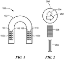
- a structure 100 which can be part of a current sensor described below in conjunction with FIG. 5 , can include a current conductor 102.
- the current conductor can be formed as an open loop for which current travels in two different directions.
- the structure 100 can also include four TMR elements 104, 106, 108, 110.
- Each TMR element can be comprised of a plurality of so-called "pillars.” Four pillars are shown for each one of the TMR elements 104, 106, 108, 110. However, in other embodiments each TMR element can include a different number of pillars, fewer than or greater than four pillars. In some embodiments, each TMR element has approximately thirty pillars.
- the structure 100 can include four coils, here expanded as two coils 206, 208.
- a pillar 200 can be the same as or similar to one of the pillars of the TMR elements 104, 106, 108, 110. It should be understood that the coil 206 can generate a magnetic field with the direction indicated by an arrow 202, and the coil 208 can generate a magnetic field with a direction indicated by an arrow 204. The coils and the magnetic directions are described more fully in figures below.
- FIGS. 3 and 3A describe illustrative GMR and TMR elements, respectively. It will be understood that TMR elements are used in various descriptions herein. However, GMR elements can be used in place of the TMR elements.
- an illustrative double pinned GMR element 300 can be comprised of a stack of layers 304-326 disposed upon a surface of a substrate 302.
- driving current can run across the layers of a GMR stack of layers, i.e., parallel to the surface of the substrate 302. However, in some embodiments, the driving current can run through the layers in a direction perpendicular to the substrate 302.
- the GMR element 300 can have a maximum response axis that is parallel to the surface of the substrate and that is in a direction 328 perpendicular to zero field magnetic directions of the free layers 312, 314, and also parallel to the field generated by the reference layers, most notably the pinned layer 318.
- the GMR element 300 is double pinned, i.e., it has two pinning layers 306, 324.
- a synthetic antiferromagnet (SAF) pinned layer structure 318, 320, 322 is magnetically coupled to the pinning layer 324.
- the layers 324, 322, 320, 318 are collectively referring to as reference layers.
- the single layer pinned layer 308 is magnetically coupled to the pinning layer 306.
- the layers 306, 308 are collectively referred to bias layers. At zero external magnetic field, the free layers 312, 314 take on a magnetic alignment parallel to the bias layers 306, 308, with direction (ferromagnetic or antiferromagnetic coupling) determined by thickness and material of the spacer layer 310.
- Single pinned arrangements are also possible with one pinning layers and one pinned layer. Advantages of double pinned versus double pinned arrangement are known.
- the single layer pinned layer 308 is replaced by another SAF structure.
- the SAF structure 318, 320, 322 is replaced by a single layer pinned layer.
- the GMR element 300 has a maximum response axis (maximum response to external fields) aligned with the arrow 328, i.e., perpendicular to bias directions experienced by the free layers 312, 314, and parallel to magnetic fields of the reference layers, notably pinned layer 318. Also, in general, it is rotations of the magnetic direction of the free layers 312, 314, caused by external magnetic fields that result in changes of resistance of the GMR stack 300.
- a conventional current sensor may directly sense magnetic fields that are in the direction of the arrow 328, which are generated by sensed currents (which are not the above mentioned-currents that drive the GMR element 300).
- the sensed current generates external magnetic fields either into or out of the page, i.e., parallel to magnetic fields of the free layers 312, 314 and parallel to magnetic fields of the bias layers 306, 308.
- Magnetic fields in these directions due to sensed current tend to increase or decrease a sensitivity of the GMR element 300, sensitivity along the direction 328.
- the external magnetic fields parallel to the magnetic fields of the bias layers 306, 308 tend to add to or subtract from fields in this direction experience by the free layers 312, 314. It will become apparent that the sensitivity shift is sensed by circuits and techniques herein, and thus, it is the sensitivity shift that represents the sensed current.
- an illustrative TMR element 350 can have a stack 350 of layers 358, 306-310, 356, 354, 352, 320-326 indicative of one pillar of a multi-pillar TMR element.
- a driving current running through the TMR element 350 runs through all of the layers of the stack, running between seed and cap layers 358 and 326, i.e., perpendicular to a surface of the substrate 302.
- the TMR element 350 can have a maximum response axis that is parallel to the surface of the substrate and that is in the direction 328 perpendicular to zero field magnetic directions of the free layer 356, and also parallel to the bias field generated by the reference layers, most notably in the pinned layer 352.
- the TMR element 350 is double pinned, i.e., it has two pinning layers 306, 324.
- a synthetic antiferromagnet (SAF) pinned layer structure 352, 320, 322 is magnetically coupled to the pinning layer 324.
- the layers 324, 322, 320, 352 are collectively referring to as reference layers.
- the single layer pinned layer 308 is magnetically coupled to the pinning layer 306.
- the layers 306, 308 are collectively referred to as bias layers. With zero external magnetic field, the free layer 356 takes on a magnetic alignment parallel to the bias layers 306, 308, with direction (ferromagnetic or antiferromagnetic coupling) determined by thickness and material of the spacer layer 310.
- the single layer pinned layer 308 is replaced by another SAF structure.
- the SAF structure 352, 320, 322 is replaced by a single layer pinned layer.
- the TMR element 350 has a maximum response axis (maximum response to external fields) aligned with the arrow 328, i.e., perpendicular to bias directions experienced by the free layer 356, and parallel to magnetic fields of the reference layers, notably pinned layers 352. Also, in general, it is rotations of the magnetic direction of the free layer 356 caused by external magnetic fields that result in changes of resistance of the TMR element 350.
- a conventional current sensor may directly sense magnetic fields that are in the direction of the arrow 328, which are generated by sensed currents (which are not the above mentioned-currents that drive the TMR element 350).
- the sensed current generates external magnetic fields either into or out of the page, i.e., parallel to magnetic fields of the free layer 356 and parallel to magnetic fields of the bias layers 306, 308.
- Magnetic fields in these directions due to sensed current i.e., external magnetic field
- the external magnetic fields parallel to the magnetic fields of the bias layers 306, 308 tend to add to or subtract from fields in this direction experienced by the free layer 356.
- the sensitivity shift is sensed by circuits and techniques herein, and thus, it is the sensitivity shift that represents the sensed current.
- illustrative TMR elements 400 include a first TMR element 402 and a second TMR element 404. Each one of the TMR elements includes a respective four TMR pillars that extend upward from a surface of a substrate on which the TMR elements 402, 404 are formed. As described above, a TMR element can have more than four or fewer than four pillars.
- the TMR elements 400 are the same as TMR elements 104, 106 or TMR elements 108, 110 of FIG. 1 , but here shown in expanded form to better show the coils 406, 408, which can be the same as or similar to the coils 208, 206 of FIG. 2 .
- the feedback coils 408 are not formed.
- the TMR element 350 is shown in side view, but the TMR elements 402, 404 are shown in top view.
- the TMR element pillars are oriented such that the maximum response axis 328 is parallel to the perturbing magnetic fields generated by the perturbing coil 406, i.e., between right and left on the page of FIG. 3A but between top and bottom on the page of FIG. 4 .
- the TMR element pillars can be oriented such that the maximum response axis 328 is perpendicular to the current conductor (external) magnetic fields generated by the sensed currents 501 of FIG. 5 .
- the TMR element pillars can be oriented such that magnetic directions of the reference layers of the TMR element 350 are perpendicular to the current conductor magnetic fields generated by the sensed currents.
- the TMR element pillars are also oriented such that a direction of bias magnetic fields in the bias layers 306, 308 is parallel to a feedback magnetic field generated by the feedback coil 408, i.e., into and out of the page on FIG. 3A , but between right and left on the page of FIG. 4 , which is also parallel to, but opposing, sensed magnetic fields generated by the sensed current.
- fields generated by the feedback coil 408 are used to oppose (and are parallel to) fields resulting from sensed current in the current conductor102 of FIG. 1 , which are also parallel to fields in the bias layers 306, 308 of FIG. 3A .
- the feedback coil 408 can generate a feedback magnetic field that fully opposes the sensed magnetic field generated by the sensed currents in a current conductor.
- the feedback coil arrangement can result in no sensitivity shift at the TMR elements 400.
- current in the feedback coil 408 can be indicative of a sensitivity shift that would have occurred were it not for the feedback arrangement and the feedback coil 408.
- the current in the feedback coils can be indicative of the sensitivity shift that would have occurred.
- Advantages of feedback arrangements include, but are not limited to, and ability to keep the TMR or GMR element operating at a near zero magnetic field, i.e., within a linear region of a transfer characteristic of the TMR or GMR element.
- a near zero magnetic field i.e., within a linear region of a transfer characteristic of the TMR or GMR element.
- a magnetic field sensor 500 can include four TMR elements 504, 506, 508, 510 disposed upon a substrate 510 along with an electronic circuit 512.
- the magnetic field sensor can also include a current conductor 502 through which a sensed current 501, Ip+, Ip- that the magnetic field sensor 500 is operable to measure, can flow.
- a sensed current 501 Ip+, Ip- that the magnetic field sensor 500 is operable to measure
- the sensed current 501 is described herein to be a DC sensed current.
- the same techniques apply to an AC measure current.
- the current conductor 502 is an open loop, the current 501 flows in two different directions Ip-, Ip+.
- the current conductor 502 has two current conductor portions 502a, 502b.
- the current 501 results in two different direction magnetic fields represented by arrows 503a, 503b.
- maximum response axes of the four TMR element 504, 506, 508, 510 are parallel to the long axis of the TMR elements, i.e., between top and bottom of the page, and are all in the same direction.
- perturbing magnetic fields generated by perturbing coils e.g., 406 of FIG. 4 , are generated.
- the fields in the bias layers e.g., 306, 308 of FIG. 3A are aligned between right and left on the page of FIG. 5 and all have the same direction.
- the sensed current magnetic fields 503a, 503b are aligned with the bias magnetic fields (between right and left) and not with the maximum response axis (between top and bottom). Since the sensed magnetic fields 503a, 503b are in opposite directions, sensitivity of two of the TMR elements, e.g., 504, 506, moves in one direction, e.g., increases, and sensitivity of the other two TMR elements, e.g., 508, 510, moves in the other direction, e.g., decreases.
- the current conductor 502 can be part of a lead frame of the magnetic field sensor 500, which can terminate at two of a plurality of leads in the lead frame. In other embodiments, the current conductor 502 is not part of the magnetic field sensor, but is instead a separate conductor, for example, a current conductor on a circuit board to which the magnetic field senor 500 is mounted.
- the TMR elements 504, 506 are labeled as left, L, and the TMR elements 508, 510 are labeled right, R.
- the left and right designations are arbitrary and are used to indicate that the TMR elements 504, 506 experience the magnetic field 503a that is in a different direction from the magnetic field 503b experience by the TMR elements 508, 510.
- left and right also indicate left and right sides of FIG. 5 .
- the different directions result from the two different directions in which the sensed current 501 flows in the current conductor 502.
- TMR elements 504, 506, 508, 510 are shown, in other embodiments, there can be two TMR elements, one disposed on the left and one disposed on the right. In other embodiments, there can be more than four TMR elements, with half on the left and half on the right.
- an electronic circuit 600 used in illustrative magnetic field sensors described in conjunction with figures below, can include first and second magnetoresistance elements 602, 604, e.g., TMR elements.
- the magnetoresistance element 602 can receive a driving current from a current source 606.
- the magnetoresistance element 604 can receive a driving current from a current source 608.
- Voltages 602a, 604a are generated by the first and second magnetoresistance elements 602, 604, respectively, which are responsive to magnetic fields.
- a differential amplifier 610 is coupled to the first and second magnetoresistance elements 602, 604.
- Reasons for the difference are described in conjunction with figures below.
- an electronic circuit 700 used in illustrative magnetic field sensors described in conjunction with figures below, can include first, second, third, and fourth magnetoresistance elements 702, 704, 706, 708, e.g., TMR elements arranged in a full bridge arrangement.
- the full bridge arrangement can be coupled between a voltage source 710 and a reference voltage, e.g., a ground voltage.
- Voltages 700a, 700b are generated by the full bridge, both of which are responsive to magnetic fields. A difference between the voltages 700a, 700b is automatically generated by the full bridge arrangement.
- a differential amplifier 712 can be coupled to the full bridge arrangement.
- the differential amplifier 712 is operable to generate a difference signal 712a that is also a difference of the voltages 700a, 700b.
- Reasons for the difference are described in conjunction with figures below.
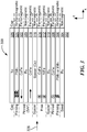
- graphs 800 have vertical ranges in amplitude, for example, volts in arbitrary units, and horizontal ranges in time in arbitrary units.
- the sensed currents can be AC currents.
- Graph 802 is indicative of an AC signal 802a generated by the left magnetoresistance element(s), e.g., one of, or both of, the magnetoresistance elements 504, 506 of FIG. 5 , when the sensed current, e.g., 501 of FIG. 5 , is zero.
- the AC part of the signal is a result of the perturbing magnetic field described above in conjunction with FIG. 4 , generated by the coil 406, which, as described above, can be aligned with a maximum response axis of the left magnetoresistance element(s).
- the perturbing magnetic field can have a constant amplitude.
- the perturbing magnetic field, and the resulting AC signal 802a can have a high frequency, e.g., one megaHertz.
- Graph 804 is indicative of an AC signal 804a generated by the right magnetoresistance element(s), e.g., one of or both of the magnetoresistance elements 508, 510 of FIG. 5 , when the sensed current, e.g., 501 of FIG. 5 , is zero.
- the AC part of the signal is a result of the perturbing magnetic field also described above in conjunction with FIG. 4 , generated by the coil 406, which, as described above, can be aligned with a maximum response axis of the right magnetoresistance element(s).
- Graph 806 shows a signal 806a indicative of a difference between the AC signals 802a, 804a.
- the difference is the signal 806a with an AC amplitude of zero.
- Graph 808 is indicative of an AC signal 808a generated by the left magnetoresistance element(s), e.g., one of or both of the magnetoresistance elements 504, 506 of FIG. 5 , in response to the perturbing magnetic field(s) generated by the perturbing coils(s), when the sensed current, e.g., 501 of FIG. 5 , is greater than zero.
- the AC part of the signal 808a is a result of the perturbing magnetic field described above in conjunction with FIG. 4 , generated by perturbing coils proximate to the left magnetoresistance element(s), e.g., 406, which, as described above, can be parallel to a maximum response axis of the left magnetoresistance element(s).
- the signal 808a is greater in amplitude than the signal 802a due to an effect of the magnetic field generated by the non-zero sensed current, e.g., the magnetic field 503a generated by the measure current 501 of FIG. 5 .
- the magnetic field generated by the sensed current in a direction parallel to magnetic fields in the bias layers 306, 308 of FIG. 4 , has the effect of changing a sensitivity of the left magnetoresistance element(s), here shown to be an increase of sensitivity.
- the magnetic field generated by the sensed current 501 has an indirect influence upon the signal 808a.
- Graph 810 is indicative of an AC signal 810a generated by the right magnetoresistance element(s), e.g., one of or both of the magnetoresistance elements 508, 510 of FIG. 5 , in response to the perturbing magnetic field(s) generated by the perturbing coils(s), when the sensed current, e.g., 501 of FIG. 5 , is greater than zero.
- the AC part of the signal 810a is a result of the perturbing magnetic field described above in conjunction with FIG. 4 , generated by perturbing coils proximate to the right magnetoresistance element(s), e.g., 406, which, as described above, can be parallel to a maximum response axis of the right magnetoresistance element(s).
- the signal 810a is lower in amplitude than the signal 804a due to an effect of the magnetic field generated by the non-zero sensed current, e.g., the magnetic field 503b generated by the sensed current 501 of FIG. 5 , and which is in a direction opposite to the magnetic field 503a.
- the magnetic field generated by the sensed current in a direction parallel to magnetic fields in the bias layers 306, 308 of FIG. 4 , has the effect of changing a sensitivity of the left magnetoresistance element(s), here shown to be a decrease of sensitivity.
- the magnetic field generated by the sensed current 501 has an indirect influence upon the signal 810a.
- Graph 812 shows a signal 812a indicative of a difference between the AC signals 808a, 810a.
- the difference is the signal 812a with a non-zero AC amplitude.
- Amplitude of the signal 812a is indicative of an amplitude of the sensed current 501.
- Phase of the signal 812a is indicative of a direction of the sensed current 501.
- Graph 814 is indicative of an AC signal 814a generated by the left magnetoresistance element(s), e.g., one of or both of the magnetoresistance elements 504, 506 of FIG. 5 , in response to the perturbing magnetic field(s) generated by the perturbing coils(s), when the sensed current, e.g., 501 of FIG. 5 , is less than zero.
- the AC part of the signal 814a is a result of the perturbing magnetic field described above in conjunction with FIG. 4 , generated by perturbing coils proximate to the left magnetoresistance element(s), e.g., 406, which, as described above, can be parallel to a maximum response axis of the left magnetoresistance element(s).
- the signal 814a is smaller in amplitude than the signal 802a due to an effect of the magnetic field generated by the non-zero sensed current, e.g., the magnetic field 503a generated by the measure current 501 of FIG. 5 , but now reversed versus field 503b.
- the magnetic field generated by the sensed current in a direction parallel to magnetic fields in the bias layers 306, 308 of FIG. 4 . has the effect of changing a sensitivity of the left magnetoresistance element(s), here shown to be a decrease of sensitivity.
- the magnetic field generated by the sensed current 501 has an indirect influence upon the signal 814a.
- Graph 816 is indicative of an AC signal 816a generated by the right magnetoresistance element(s), e.g., one of or both of the magnetoresistance elements 508, 510 of FIG. 5 , in response to the perturbing magnetic field(s) generated by the perturbing coils(s), when the sensed current, e.g., 501 of FIG. 5 , is lesser than zero.
- the AC part of the signal 816a is a result of the perturbing magnetic field described above in conjunction with FIG. 4 , generated by perturbing coils proximate to the right magnetoresistance element(s), e.g., 406, which, as described above, can be parallel to a maximum response axis of the right magnetoresistance element(s).
- the signal 816a is higher in amplitude than the signal 804a due to an effect of the magnetic field generated by the non-zero sensed current, e.g., the magnetic field 503b generated by the sensed current 501 of FIG. 5 , and which is in a direction aligned with the magnetic field 503a.
- the magnetic field generated by the sensed current in a direction parallel to magnetic fields in the bias layers 306, 308 of FIG. 4 , has the effect of changing a sensitivity of the left magnetoresistance element(s), here shown to be a decrease of sensitivity.
- the magnetic field generated by the sensed current 501 has an indirect influence upon the signal 814a.
- Graph 818 shows a signal 818a indicative of a difference between the AC signals 812a, 812b.
- the difference is the signal 818a with a non-zero AC amplitude.
- Amplitude of the signal 818a is indicative of an amplitude of the sensed current 501.
- Phase of the signal 818a is indicative of a direction of the sensed current 501.
- the signal 818a (and 816a, 814a) is opposite in phase from (one hundred eighty degrees apart from) the signal 812a, which is indicative of the different directions of the sensed current.
- the graphs 800 are indicative of DC sensed magnetic fields, e.g., 503a, 503b of FIG. 5 , generated by a DC current, e.g., 501 of FIG. 5 .
- the same techniques apply to AC sensed magnetic fields generated by and AC sensed current.
- the AC sensed current has a frequency or bandwidth less than a frequency of the perturbing magnetic fields, e.g., frequency of the signals in the graphs 800.
- the frequency or bandwidth of the AC sensed current is less than one half of the frequency of the perturbing magnetic fields.
- the frequency or bandwidth of the AC sensed current is less than one fifth or less than one tenth of the frequency of the perturbing magnetic fields.
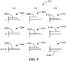
- graphs 900 show DC signals 902a, 904a, 906a, 908a, 910a, 912a, 914a, 916a, 918a that are indicative of AC amplitudes of the signals 802a, 804a, 806a, 808a, 810a, 812a, 814a, 816a, 818a, respectively.
- the signal 918a is shown as a negative amplitude, which is indicative of the signal 818a being one hundred eighty degrees out of phase from the other signals. Compare signals 912a and 918a and also signals 812a and 818a.
- the signal 918a with an opposite sign is an outcome of the signal 918a being a difference of signals 914a and 916a.
- a magnetic field sensor 1000 can include four magnetoresistance elements coupled together in a full bridge arrangement 1002, which can be the same as or similar to the full bridge arrangement 700 of FIG. 7 .
- First and second magnetoresistance elements, La, Lb can both be disposed proximate to each other and on the left side, for example, on the left side of the current conductor 502 of FIG. 5 .
- Third and fourth magnetoresistance elements Ra, Rb can both be disposed proximate to each other and on the right side, for example, on the right side of the current conductor 502 of FIG. 5 .
- the full bridge arrangement 1002 can be coupled between a voltage source and a reference voltage, e.g., a ground voltage.
- a first perturbing coil 1020 can be disposed proximate to the first magnetoresistance element, La, a second perturbing coil 1022 can be disposed proximate to the second magnetoresistance element, Lb, a third perturbing coil 1024 can be disposed proximate to the third magnetoresistance element, Ra, and a fourth perturbing coil 1026 can be disposed proximate to the fourth magnetoresistance element, Rb.
- a clock signal generator 1016 can generate a voltage signals 1016a coupled to a resistor 1018.
- a current signal 1018a can drive the first, second, third, and fourth perturbing coils 1022, 1022, 1024, 1026 in series.
- first, second, third, and fourth perturbing coils 1022, 1022, 1024, 1026 along with the clock signal generator 1016 and the resistor 1018 are referred to herein as a perturbing magnetic field signal generator 1014.
- the difference signal 1004a is already a signal that represents a difference of signals generated by magnetoresistance elements on the left and right sides, for example left and right sides of the current conductor 502 of FIG. 5 .
- a differential signal 1002a, 1002b generate by the bridge circuit 1002 can be received by a differential amplifier 1004.
- the amplifier 1004 can generate a difference signal 1004a.
- the difference signal 1004a like the difference signal 712a of FIG. 7 , is a signal that represents a difference of signals generated by magnetoresistance elements on the left and right sides, for example left and right sides of the current conductor 502 of FIG. 5 .
- the difference signal 1004a can be received by a capacitor 1006, which can be coupled to a demodulator 1008, which can be coupled to a filter 1010, which can be coupled to an analog-to-digital converter 1012 to generate a digital signal 1012a.
- the demodulator 1008 and the filter 1010 form an amplitude detecting circuit.
- the demodulator 1008 can be replaced by a full wave rectifier circuit.
- Values of the digital signal 1012a can be indicative of values of the sensed current signal 1009.
- the first, second, third and fourth magnetoresistance elements La, Lb, Ra, Rb can have maximum response axes between top and bottom on the page.
- the first, second, third and fourth perturbing coils can be operable to generate first, second, third, and fourth AC perturbing magnetic fields (e.g., 1415, 1417), respectively, between top and bottom on the page. Therefore, the first, second, third and fourth magnetoresistance elements La, Lb, Ra, Rb are directly responsive to the first, second, third, and fourth AC perturbing magnetic fields.
- Coils 1032, 1036 are indicative of magnetic fields 1036, 1042 generated by a current 1034 passing through two portions of a current conductor proximate to the first, second, third and fourth magnetoresistance elements La, Lb, Ra, Rb, e.g., the current 501 of FIG. 5 .
- the magnetic fields 1036, 1042 can be perpendicular to directions of maximum response axes of the first, second, third and fourth magnetoresistance elements La, Lb, Ra, Rb, i.e., between left and right on the page. This direction can be parallel to bias directions of the first, second, third and fourth magnetoresistance elements La, Lb, Ra, Rb.
- the magnetic fields 1036, 1042 can influence sensitivities of the of first, second, third and fourth magnetoresistance elements La, Lb, Ra, Rb.
- the difference signal 1004a can be an AC voltage signal, with a frequency equal to a frequency of the clock signal 1022a and a magnitude influenced by the coils 1032, 1038.
- a sensed current 501 carried by the sensed current conductor 502 of FIG. 5 i.e., a sensed current 1034 (i.e., a local current 1034) carried by the first and second coils 1032, 1038, are described herein to be DC currents, merely for clarity.
- the first coil 1032 generates a magnetic field with a first direction indicated by arrow 1036
- the second coil 1038 generates a magnetic field with a second direction indicated by an arrow 1042.
- the first and second directions 1036, 1038 are in opposite directions from each other.
- the magnetic fields with first and second directions 1036, 1038, respectively result in opposite direction changes of sensitivity of the first and second magnetoresistance element La, Lb versus the third and fourth magnetoresistance element Ra, Rb.
- the changes of sensitivity are represented by the graphs 800 of FIG. 8 .
- the amplifier 1004 is coupled to receive the differential voltage signal 1002a, 1002b, which, as described above, can be an AC voltage signal like the signals 802a, 808a, 814a of FIG. 8 , having an AC frequency equal to a frequency of the clock signal 1022a, and having an amplitude in accordance with an amplitude of the sensed (i.e., local) magnetic field having the directions 1036, 1038.
- the amplitude detecting circuit 1008, 1010 result in signals in a first two rows of graphs 800 turning into signals in a first two rows of graphs 900.
- Values of the converted signal 1012a are directly related to values of the measured current 1034.
- the magnetic field sensor 1000 which uses the perturbing magnetic fields with directions 1015, 1017 to indirectly measure the sensed current 1034 has advantages over a conventional magnetic field sensor that directly measures the sensed current 1034.
- the capacitor 1006 can block DC portions of signals to generate the AC coupled signal 1006a, any undesirable effects that may result from undesirable DC offset voltages generated by the first, second, third, and fourth magnetoresistance elements La, Lb, Ra, Rb can be reduced or eliminated. This is an advantage both for GMR and TMR elements.
- the magnetic field sensor 1000 can use either TMR elements or GMR elements as the first, second, third, and fourth magnetoresistance elements La, Lb, Ra, Rb, the magnetic field sensor 1000 is well suited for use of the TMR elements. It is known that TMR elements tend to have higher sensitivities than GMR elements. It is also known that TMR elements tend to have worse electrical noise and worse signal to noise ratios at low frequencies that GMR elements. Because the magnetic field sensor 1000 actually operates with relatively high frequencies generated by the clock signal generator 1016, the TMR elements, which have higher sensitivity that GMR elements, can avoid the higher noise at low frequencies
- the magnetic field sensor 1000 is an open loop magnetic field sensor having no feedback loop from the digital signal 1012a to an earlier point in the magnetic field sensor 1000. Feedback magnetic field sensors with closed loop feedback are also possible.
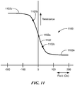
- a graph 1100 has a horizontal axis with a scale in units of magnetic field in Oersteds (Oe) and a vertical axis with a scale in units of resistance in arbitrary units.
- a curve 1102 is representative of a resistance transfer function of a double pinned magnetoresistance element, i.e., resistance versus magnetic field experienced by the double pinned magnetoresistance element.
- the resistance transfer function 1102 has a linear region 1102a between an upper saturation point 1102b and a lower saturation point 1102c. Regions 1102d, 1102e are in saturation. It should be understood that the linear region 1102a is not a perfectly straight line linear region.
- the resistance transfer function 1102 is shown symmetrical about zero magnetic field. However, a double pinned magnetoresistance element tends to have a shape similar to the resistance transfer function 1102, but offset somewhat from zero magnetic field, particularly when reference and bias directions are not precisely orthogonal to each other.
- a slope at a point on the resistance transfer function 1102 is equivalent to a sensitivity (e.g., ohms per oersted) of the illustrative double pinned magnetoresistance element at that point (i.e., at a particular external magnetic field).
- a double pinned GMR or TMR element has a linear region that is not a perfectly straight line.
- FIGS. 12-15 show current sensors similar to the current sensor of FIGS. 5 and 10 , but include not only a plurality of magnetoresistance elements arranged in a bridge operable to sense a current, but also a single magnetoresistance element operable to sense a stray magnetic field. Circuits described in conjunction with FIGS. 16 , 17 , 24 , and 25 can use the sensed stray field to correct for errors in the sensed current. The circuits described in conjunction with FIGS. 18 and 26 can be disposed upon common substrates, respectively.
- FIGS. 12-15 show the signal magnetoresistance element
- the single magnetoresistance element can be replaced by a plurality of magnetoresistance elements coupled in series or in parallel or any combination of series and parallel, with respective reference layer magnetic directions parallel to each other.
- Maximum response axes can be parallel to the magnetic directions of the reference layers. However, in other embodiments, the maximum response axes are not parallel to the reference directions.
- the stray field sensor can be used to sense a stray (external) magnetic field associated with any magnetic field sensor.
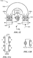
- a current sensor 1200 can include aspects of the current sensor of FIG. 5 .
- Current conductor 1202 with current conductor portions 1202a, 1202b can be the same as or similar to the current conductor 502 with current conductor portion 502a, 502b.
- Magnetoresistance elements A, B, D, E can be the same as or similar to the magnetoresistance elements La, Lb, Ra, Rb, respectively, of FIGS. 5 and 7 .
- Current 1204 can be the same as or similar to the current 501 of FIG. 5 .
- Magnetic field directions 1206a, 1206b can be the same as or similar to the magnetic field directions 503a, 503b of FIG. 5 .
- Circuit 1212 can include circuit portions of the circuit 512 of FIG. 5 such as the circuit 1000 of FIG. 10 but can include additional circuit portions described below in conjunction with FIGS. 18 or 25 .
- dashed arrows are representative of reference directions (which can be maximum response directions) of the magnetoresistance elements A, B, D, E, which are parallel to each other. This is also the reference direction of the reference layer structures of FIGS. 3 and 3A .
- Orthogonal coordinates x and y are used to describe and x-y plane in figures herein.
- the current sensor 1200 can include a single (or magnetoresistance element C (or, as described above, a plurality of magnetoresistance elements with parallel reference layer magnetic directions) disposed at a position so that the magnetoresistance element C is generally responsive to external magnetic fields parallel to the y axis and not responsive to magnetic fields in directions parallel to the x axis, e.g., magnetic fields indicated by arrows 1206a, 1206b that the current sensor and magnetoresistance elements A, B, D, E attempt to measure.
- the single magnetoresistance element C has a reference direction indicated by a dashed arrow, which can also be the direction of maximum response of the magnetoresistance element C.
- the single magnetoresistance element 1208 can be disposed at a position at which the single magnetoresistance element 1208 is substantially not responsive to magnetic fields generated by the current 1204. In essence, at the position of the single magnetoresistance element 1208, magnetic fields generated by the current 1204 tend to be in a z direction, to which the single magnetoresistance element C is substantially not responsive.
- magnetoresistance elements A, B, C, D, E can have the same structure and the same internal magnetic directions.
- a coil 1208 or other magnetic field generating structure can be disposed proximate to the single magnetoresistance element C.
- the coil 1208 can be operable to generate an AC magnetic field in a direction of an arrow 1210 parallel to the y axis.
- the four magnetoresistance elements A, B, D, E can be arranged in a full bridge coupled between a power supply voltage and a reference voltage, for example, ground.
- a differential voltage V can be generated by the full bridge arrangement.
- the full bridge arrangement can be the same as or similar to the full bridge arrangement 700 of FIG. 7 .
- FIG. 12B which includes the single magnetoresistance element C of FIG. 12 , can be driven with a current generator to achieve a voltage signal.
- FIG. 17 , 18 , 25 , and 26 described below describe driving the single magnetoresistance element C with a voltage source to achieve a current signal followed by a current mirror circuit and a resistor to achieve a voltage signal.
- the two ways of driving the magnetoresistance element C result in similar voltage signals.
- graphs shown below describe resistances, which are directly related to the above-described current signals.
- a current sensor 1300 can include not only a coil 1308 or other magnetic field generating structure like the coil 1208 of FIG. 1 , but also another coil 1312 or other magnetic field generating structure disposed proximate to the single magnetoresistance element C.
- the coil 1308 can generate an AC magnetic field in a direction of an arrow 1310 and the coil 1312 can generate an AC magnetic field in a direction of an arrow 1314.
- Magnetic field directions 1306a, 1306b can be the same as or similar to the magnetic field directions 503a, 503b of FIG. 5 .
- FIGS. 13A and 13B will be understood from the discussion above about FIGS. 12A and 12B .
- a current sensor 1400 can include aspects of the current sensor of FIG. 5 .
- Current conductor 1402 with current conductor portions 1402a, 1402b can be the same as or similar to the current conductor 502 with current conductor portion 502a, 502b.
- Magnetoresistance elements A, B, D, E can be the same as or similar to the magnetoresistance elements La, Lb, Ra, Rb, respectively, of FIGS. 5 and 7 .
- Current 1404 can be the same as or similar to the current 501 of FIG. 5 .
- Magnetic field directions 1406a, 1406b can be the same as or similar to the magnetic field directions 503a, 503b of FIG. 5 .
- the magnetoresistance element A, B, D, E of FIG. 12 are shown to be GMR elements, the magnetoresistance element A, B, D, E of FIG. 15 are shown to be TMR elements, each TMR element having a plurality of TMR pillars coupled in series.
- Circuit 1412 can include circuit portions of the circuit 514 of FIG. 5 such as the circuit 1000 of FIG. 10 but can include additional circuit portions described below in conjunction with FIGS. 18 or 26 .
- dashed arrows are representative of parallel reference directions (which can be parallel to maximum response directions of the magnetoresistance elements A, B, D, E). This is also the reference direction of the reference layer structures of FIGS. 3 and 3A .
- the current sensor 1400 can include a single magnetoresistance element C having a plurality of TMR pillars (or, as described above, a plurality of magnetoresistance elements, each having a plurality of TMR pillars and each with reference magnetic directions parallel to each other) disposed at a position so that the magnetoresistance element C is generally not responsive to magnetic fields in directions indicated by arrows 1406a, 1406b that the current sensor and magnetoresistance elements A, B, D, E attempt to measure.
- the magnetoresistance element C has a reference direction indicated by a dashed arrow parallel to the other reference directions, which can also be the direction of maximum response of the magnetoresistance element C.
- the magnetoresistance element C in FIG. 14 is shown to be a TMR element having a plurality of pillars.
- the single magnetoresistance element 1408 can be disposed at a position at which the single magnetoresistance element 1408 is substantially not responsive to magnetic fields generated by a current 1404. In essence, at the position of the single magnetoresistance element 1408, magnetic fields generated by the current 1404 tend to be in a z direction, to which the single magnetoresistance element C is substantially not responsive.
- magnetoresistance elements A, B, C, D, E can have the same structure and the same internal magnetic directions.
- a plurality of coils 1408 or other magnetic field generating structures can be disposed proximate to the single magnetoresistance element C.
- the coils 1408 can be operable to generate a plurality of AC magnetic fields in a direction of an arrow 1410.
- FIGS. 14A and 14B will be understood from the discussion above about FIGS. 12A and 12B .
- a current sensor 1500 can include not only coils 1508 or other magnetic field generating structure like the coil 1408 of FIG. 14 , but also another coil 1512 or other magnetic field generating structure disposed proximate to the single magnetoresistance element C.
- The1508 can generate an AC magnetic field in a direction of an arrow 1510 and, the coil 1512 can generate an AC magnetic field in a direction of an arrow 1514.
- Magnetic field directions 1506a, 1506b can be the same as or similar to the magnetic field directions 503a, 503b of FIG. 5 .
- FIGS. 15A and 15B will be understood from the discussion above about FIGS. 12A and 12B .
- a TMR element 1601 can have a plurality of TMR pillars, e.g., four TMR pillars 1610, 1612, 1614, 1616, and can be the same as or similar to the TMR element 1408 of FIG. 14 .
- a plurality of coils e.g., four coils 1602, 1604, 1606, 1608, or other magnetic field generating structures such as a current conductor can be the same as or similar to the plurality of coils 1408 of FIG. 14 .
- the plurality of coils 1602, 1604, 1606, 1608 can be operable to generate a plurality of magnetic fields, e.g., four magnetic fields, parallel to a y direction and indicated by arrows, passing through the plurality of TMR pillars.
- the four TMR pillars can have respective maximum response axes parallel to a y direction.
- a circuit portion 1700 can include a one or more TMR elements, here a single TMR element 1702 having a plurality of TMR pillars, e.g., 1610, 1612, 1614, 1616 of FIG. 16 .
- the single TMR element can be driven by a voltage source 1704 to generate a current signal 1706 that changes in response to a magnetic field.
- a current mirror circuit 1708 can receive the current signal 1706 and can generate a voltage signal 1710 by a mirrored current passing through a resistor 1712.
- a plurality of coils 1728, C1, C2, C3, C4 can be the same as or similar to the plurality of coils 1602, 1604, 1606, 1608 of FIG. 16 and can be operable to generate one or more magnetic fields, e.g., four magnetic fields, indicated by an arrow 1730, all in the same direction, and all parallel to the y axis. In some embodiments, only one, or one or more, coils are used to generate magnetic fields parallel to the y axis.
- a clock generator 1722 can generate a clock signal 1722a at a frequency fc.
- the clock signal 1722a can be received by at one end of a resistor 1724.
- a current signal 1726 can result at the other end of the resistor 1724.
- the current signal 1726 can drive the plurality of coils C1, C2, C3, C4 to generate the AC magnetic fields 1730 with the frequency of fc proximate to the plurality of pillars of the TMR element 1702.
- Directions of the AC magnetic fields 1730 are parallel to the maximum response axis of the TMR element 1702.
- Current signal 1706 (and voltage signal 1710) can be comprised of a frequency component at the frequency fc that is generated by the coils C1, C2, C3, C4.
- the current signal 1706 can also be comprised of a lower frequency band of frequencies resulting from a stray (external) magnetic field sensed by the single magnetoresistance element 1702, in particular, resulting from a y component of the stray magnetic field when projected onto the x-y plane.
- the voltage signal 1710 can be AC filtered by a capacitor 1714 to generate an AC coupled signal 1716.
- a demodulator 1718 can receive the AC coupled signal 1716 and can receive the clock signal 1722a. In operation, the demodulator 1718 can multiply the AC coupled signal 1716 with the clock signal 1722a and low pass filter the result to generate a demodulated signal 1718a.
- the demodulator 1718 can include a square wave demodulator comprised of a switching circuit. It is desirable that the frequency fc be substantially above a frequency of a stray (external) magnetic field that the single TMR element senses.
- the demodulator 1718 can also include a low pass filter.
- the demodulator 1718 can essentially operate as an amplitude detecting circuit, and the demodulated signal 1718a is representative of an amplitude of the AC coupled signal 1716.
- the demodulator 1718 can be replaced with other forms of amplitude detecting circuits, for example, a rectifier and filter.
- a low pass filter 1720 can receive the AC voltage signal 1710 and can generate a filtered signal 1720a.
- a stray magnetic field with a component in a y direction when projected onto the x-y plane can result in a low frequency part of the voltage signal 1710.
- a stray magnetic field with a component parallel to the x axis when projected onto the x-y plane can amplitude modulate the signal component at the frequency fc, i.e., can generate AM sidebands around the signal component at the frequency fc of the AC coupled signal 1716.
- the amplitude modulation is the result of the x component of the stray magnetic field being parallel to the bias direction of the TMR element 1702, which can add to or subtract from the bias field experienced by free layer(s) of the TMR element 1702, essentially resulting in AC changes of the sensitivity of the TMR element 1702.
- the filtered signal 1720a is indicative of the low frequency part of the voltage signal 1710 and is primarily responsive to the y component of the stray magnetic field. A simulation of this relationship is described below in conjunction with FIG. 19 .
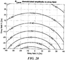
- the demodulated signal 1718a is indicative of the amplitude of the AC coupled signal 1716 and is primarily responsive to the x component of the stray magnetic field. A simulation of this relationship is described below in conjunction with FIG. 20 .
- the demodulated signal 1718a and the filtered signal 1720a can each be responsive to both the x component and the y component.
- a magnetic field sensor 1800 can be disposed upon a surface of a substrate 1801, e.g., a semiconductor substrate.
- An x-y plane can be upon the surface 1801.
- the magnetic field sensor 1800 can include an external field sensing circuit 1802 operable to sense an external (e.g., stray) magnetic field generated outside of the magnetic field sensor 1800.
- the external field sensing circuit 1802 can include a single magnetoresistance (TMR or GMR) element 1809 (or more than one with the parallel maximum response axes) driven by a voltage generator 1808 to result in a current signal 1812 and a voltage signal 1810.
- the external field sensing circuit 1802 can also include a component determination module 1804 having a capacitor 1814, a demodulator 1818, and a low pass filter 1820 the same as or similar to elements of FIG. 17 .
- the external field sensing circuit 1802 is operable to generate a demodulated signal 1818a primarily responsive to a component of stray magnetic field in the x direction, and a filtered signal 1820a primarily responsive to a component of the stray magnetic field in the y direction.
- the signals 1818a, 1820a are only primarily responsive to the stated components and each is responsive to both the x component and the y component.
- values of the signals 1818a, 1820a can be referred to as measured x-dominant values 1818a and measured-y-dominant values 1820a, respectively.
- the measured-x-dominant values 1818a are more indicative of x components and less indicative of y components of the external magnetic field projected onto the x-y plane, but are responsive to both the x component and the y component.
- the measured-y-dominant values 1820a are more indicative of the y components and less indicative of the x components of the external magnetic field projected onto the x-y plane, but are responsive to both the x component and the y component.
- the measured-x-dominant values 1818a and the measured-y-dominant values 1820a can be received by an external field processor 1822.
- a non-volatile look up table memory 1824 for example, and EEPROM, can also be coupled to the external field processor 1822.
- the non-volatile look up table memory 1824 can store a matrix of predetermined correction coefficients received as a signal 1832 from outside of the magnetic field sensor 1800 prior to operation of the magnetic field sensor 1800.
- values of the measured-x-dominant values 1818a and the values of the measured-y-dominant values 1820a can be used in combination to acquire a correction coefficient from the non-volatile look up table memory 1824, using the non-volatile look up table memory 1824 as a look up table.
- the external field processor can send a control signal 1822a to the non-volatile look up table memory 1824 in accordance with the combination of the measured-x-dominant values 1818a and the measured-y-dominant values 1818b.
- the external field processor 1822 can identify a selected one of the correction factors to generate a selected correction coefficient 1822b in accordance with the measured x-dominant values 1818a and the measured y-dominant values 1822a.
- the magnetic field sensor 1800 can also include a local magnetic field sensing circuit 1806, which, for example, can be like the magnetic field sensor 1000 of FIG. 10 , but which is here shown in more generic blocks.
- the local magnetic field sensing circuit 1806 can include a bridge circuit 1826 to generate a differential magnetic field signal 1826a, 1826b.
- the differential magnetic field signal 1826a, 1826b can be responsive to both a local magnetic field (that is desirable to sense, e.g., in the x-direction of FIG. 14 ) and also the external (stray) magnetic field having projected x and y directions sensed by the external field sensing circuit 1802.
- the differential magnetic field signal 1826a, 1826b is also referred to as a total magnetic field signal 1826a, 1826b.
- the sensing element circuit can be the same as or similar to some elements of the magnetic field sensor 1000 of FIG. 10 .
- a magnetic field generator 1832 having one or more coils can be the same as or similar to the coils magnetic field generator having the coils 1728 of FIG. 17 and can be disposed proximate to the single magnetoresistance element 1808 upon the substrate 1801.
- the sensing element circuit 1828 can be operable to generate an uncorrected signal 1828a.
- the uncorrected signal 1828a can be responsive to both the local field that is desirable to measure, and also the external (e.g., stray) magnetic field that is undesirable.
- the magnetic field sensor 1000 of FIG. 10 it is the local magnetic fields 1036, 1042 that are desirable to measure, which are generated by current flowing in the current conductor 502 of FIG. 5 .
- the local magnetic fields 1036, 1042 of FIG. 10 can be circular around the portions 1002a, 1002b of the current conductor.
- the local magnetic fields 1036, 1042 tend to intersect the single magnetoresistance element 1810 in a z direction perpendicular to the x-y plane of the substrate, a direction to which the single magnetoresistance element 1810 is not responsive.
- the magnetic field sensor 1800 can include a correction circuit 1830 to receive the uncorrected signal 1828a and to receive the selected correction coefficient value 1822b (responsive to the external (e.g., stray) magnetic field and substantially not responsive to the local magnetic field).
- the correction circuit 1830 can be operable to generate a corrected signal 1830 responsive to the local magnetic field and substantially not responsive to the external (e.g., stray) magnetic field.
- the correction circuit performs a multiplication of the uncorrected signal 1828a by the selected correction coefficient value 1822b. Thus, a more accurate measurement of the local magnetic field alone is obtained.
- a magnetic field generator 1834 can be the same as or similar to the magnetic field generator 1014 of FIG. 10 .
- a current conductor 1836 can be the same as or similar to the current conductor 1402, 1502 of FIGS. 14 or 15 .
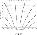
- a graph has a horizontal axis with a scale in units of an x component of a stray magnetic field projected onto the x-y plane of the substrate of FIG. 18 in Oersteds.
- the graph also has a vertical axis with a scale in units of a y component of a stray magnetic field projected onto the x-y plane of the substrate of FIG. 18 in Oersteds.
- Curves are so-called "isolines" indicative of different measured-x-dominant values of the filtered signal 1820a generated by the low pass filter 1820.
- Vertical isolines would indicate that the filtered signal 1820a is indicative of only x components of the external (e.g., stray) magnetic field.
- the isolines are not vertical, and thus, the filtered signal has values that are indicative of both x and y components of the external magnetic field.
- the isolines are somewhat vertical. Thus, the values of the signal 1820a are referred to above as the measured-x-dominant values.
- a graph has a horizontal axis with a scale in units of an x component of a stray magnetic field projected onto the x-y plane of the substrate of FIG. 18 in Oersteds.
- the graph also has a vertical axis with a scale in units of a y component of a stray magnetic field projected onto the x-y plane of the substrate of FIG. 18 in Oersteds.
- Curves are isolines indicative of different measured-y-dominant values of the demodulated signal 1818a generated by the demodulator 1818.
- Horizontal isolines would indicate that the demodulated signal 1818a is indicative of only y components of the external (e.g., stray) magnetic field.
- the isolines are not horizontal, and thus, the filtered signal has values that are indicative of both x and y components of the external magnetic field.
- the isolines are somewhat horizontal. Thus, the values of the signal 1820a are referred to above as the measured-y-dominant values.
- a graph has a horizontal axis with a scale in units of an x component of a stray magnetic field projected onto the x-y plane of the substrate of FIG. 18 in Oersteds.
- the graph also has a vertical axis with a scale in units of a y component of a stray magnetic field projected onto the x-y plane of the substrate of FIG. 18 in Oersteds.
- Curves are isolines, each indicative of a different error of the uncorrected signal 1828a of FIG. 18 .
- An error of 100% is indicative of a no error. Errors range from about 40% to about 220%. These errors are errors prior to operation of the correction circuit 1830 of FIG. 18 .
- a graph has a horizontal axis with a scale in units of ohms for the measured-x-dominated values of the demodulated signal 1818a of FIG. 18 .
- the graph also has a vertical axis with a scale in units of ohms for the measured-y-dominated values of the filtered signal 1820a of FIG. 18 .
- Curves are isolines, each indicative of a different error generated by the bridge 1826 when in the presence of the external (e.g., stray) magnetic field.
- An error of 100% is indicative of a no error. Errors range from about 50% to about 240%. These errors are errors prior to operation of the correction circuit 1830 of FIG. 18 .
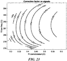
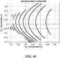
- a graph has a horizontal axis with a scale in units of ohms for the measured-x-dominated values of the demodulated signal 1818a of FIG. 18 .
- the graph also has a vertical axis with a scale in units of ohms for the measured-y-dominated values of the filtered signal 1820a of FIG. 18 .
- Curves are isolines, each indicative of a different correction factor, i.e., a value of the selected correction coefficient 1822b, when in the presence of the external (e.g., stray) magnetic field. Correction values range from about 0.5 to about 2.4, which is in concert with the curves of FIG. 22 .
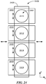
- a TMR element 2401 can have a plurality of TMR pillars, e.g., four TMR pillars 2410, 2412, 2414, 2424., and can be the same as or similar to the TMR element 1508 of FIG. 15 .
- a plurality of coils, e.g., four coils 2402, 2404, 2406, 2408, or other magnetic field generating structure can be the same as or similar to the plurality of coils 1508 of FIG. 15 .
- the plurality of coils 2402, 2404, 2406, 2408 can be operable to generate a plurality of magnetic fields, e.g., four magnetic fields, each parallel to a y axis, passing through the plurality of TMR pillars.
- Another coil 2426 can be the same as or similar to the coil 1512 of FIG. 15 .
- the coil can be operable to generate a magnetic field parallel to an x axis, indicated by arrows between left and right of the page the page, passing through the plurality of TMR pillars.
- a portion 2500 of a magnetic field sensor can include elements that will be recognized in FIG. 17 .
- a second demodulator 2504 replaces the low pass filter 1712 of FIG. 17 .
- the portion 2500 includes a second magnetic field generator 2506, 2508, 2510 for generating an AC magnetic field parallel to an x axis as indicated by an arrow 2512 and for generating a second clock signal 2506a, also labeled fy.
- the first and second AC magnetic fields 1722, 2512 can have different frequencies, both frequencies preferably substantially higher than a highest frequency of an external (e.g., stray) magnetic field. In other embodiments, the first and second AC magnetic fields 1722, 2512 can have the same frequency.
- a second capacitor 2502 can generate a second AC coupled signal 2502a received by the second demodulator 2504.
- the second demodulator can generate a second demodulated signal 2504a.
- values of the signal 1710a are measured-x-dominant- values.
- values of the signal 2504 generated by the second demodulator 2504 are measured-y-dominant values, similar to values of the filtered signal 1712a of FIG. 17
- a magnetic field sensor 2600 can be disposed upon a surface of a substrate 2601, e.g., a semiconductor substrate.
- the surface can be upon an x-y plane. Most elements of the magnetic field sensor will be recognized in FIG. 18 .
- the magnetic field sensor 2600 can include an external field sensing circuit 2602 operable to sense and external (e.g., stray) magnetic field generated outside of the magnetic field sensor 2600.
- an external field sensing circuit 2602 operable to sense and external (e.g., stray) magnetic field generated outside of the magnetic field sensor 2600.
- the external field sensing circuit 2602 can also include a component determination module 2604 having a second capacitor 2609, a first demodulator 2606, and second demodulator 2608 the same as or similar to elements of FIG. 25 .
- the external field sensing circuit 2602 is operable to generate a first demodulated signal 2606a primarily responsive to a component of stray magnetic field in the x direction, and a second demodulated signal 2608a primarily responsive to a component of the stray magnetic field in the y direction.
- the signals 2606a, 2608a are only primarily responsive to the stated components, but are each responsive to both the components of the external magnetic field in the x direction and in the y direction.
- values of the signals 2606a, 2608a can be referred to as measured-x-dominant values 2606a and measured-y-dominant values 2608a, respectively.
- the measured-x-dominant values 2606a are more indicative of x components and less indicative of a y components of the external magnetic field projected onto the x-y plane, but are responsive to both the components of the external magnetic field in the x direction and in the y direction.
- the measured-y-dominant values 2608a are more indicative of the y components and less indicative of the x components of the external magnetic field projected onto the x-y plane, but are responsive to both the components of the external magnetic field in the x direction and in the y direction.
- the measured-x-dominant values 2606a and the measured-y-dominant values 2608a can be received by an external field processor 2607.
- a non-volatile look up table memory 2610 for example, and EEPROM, can also be coupled to the external field processor 2607.
- the non-volatile look up table memory 2610 can store a matrix of correction coefficients received as a signal 2612 from outside of the magnetic field sensor 2600 prior to operation of the magnetic field sensor 2600.
- values of the measured-x-dominant values 2606a and the measured-y-dominant values 2608a can be used in combination to acquire a correction factor from the non-volatile look up table memory 2610, essentially using the non-volatile look up table memory 2610 as a look up table.
- the external field processor 2607 can send a control signal 2607a to the non-volatile look up table memory 2610 in accordance with the combination of the measured-x-dominant values 2606a and the measured-y-dominant values 2608b.
- the external field processor 2607 can use selected ones of the predetermined x values 2610a and selected ones of the predetermined y values 2610b to generate a selected correction coefficient value2607b.
- Two magnetic field generators 2614 each having one or more coils, can be the same as or similar to the magnetic field generators having the coils C1, C2, C3, C4, C5 of FIG. 25 and can be disposed upon the substrate 2601.
- the magnetic field sensor can include a correction circuit 2616 to receive the uncorrected signal 1828a (responsive to both the local and external magnetic fields) and to receive the selected correction coefficient value 2607b (responsive to the external (e.g., stray) magnetic field and substantially not responsive to the local magnetic field).
- the correction circuit 2616 can be operable to generate a corrected signal 2616a responsive to the local magnetic field and substantially not responsive to the external magnetic field.
- the correction circuit performs a multiplication of the uncorrected signal 1828a by the selected correction coefficient value 2607b. Thus, a more accurate measurement of the local magnetic field alone is obtained.
- a graph has a horizontal axis with a scale in units of an x component of a stray magnetic field projected onto the x-y plane of the substrate of FIG. 26 in Oersteds.
- the graph also has a vertical axis with a scale in units of a y component of a stray magnetic field projected onto the x-y plane of the substrate of FIG. 26 in Oersteds.
- Isolines are indicative of different measured-x-dominant values of the second demodulated signal 2608a generated by the second demodulator 2608.
- Vertical isolines would indicate that the second demodulated signal 2608a is indicative of only x components of the external (e.g., stray) magnetic field.
- the isolines are not vertical, and thus, the second demodulated signal has values that are indicative of both x and y components of the external magnetic field.
- the isolines are somewhat vertical. Thus, the values of the signal 2608a are referred to above as the measured-x-dominant values.
- a graph has a horizontal axis with a scale in units of an x component of a stray magnetic field projected onto the x-y plane of the substrate 2601 of FIG. 26 in Oersteds.
- the graph also has a vertical axis with a scale in units of a y component of a stray magnetic field projected onto the x-y plane of the substrate of FIG. 26 in Oersteds.
- Curves are isolines indicative of different measured-y-dominant values of the first demodulated signal 2606a generated by the first demodulator 2698.
- Horizontal isolines would indicate that the first demodulated signal 2606a is indicative of only y components of the external (e.g., stray) magnetic field.
- the isolines are not horizontal, and thus, the first demodulated signal 2606a has values that are indicative of both x and y components of the external magnetic field.
- the isolines are somewhat horizontal. Thus, the values of the signal 2606a are referred to above as the measured-y-dominant values.
- a graph has a horizontal axis with a scale in units of an x component of a stray magnetic field projected onto the x-y plane of the substrate 2601 of FIG.26 in Oersteds.
- the graph also has a vertical axis with a scale in units of a y component of a stray magnetic field projected onto the x-y plane of the substrate of FIG. 26 in Oersteds.
- Curves are isolines, each indicative of a different error of the uncorrected signal 1828a of FIG. 26 . Errors range from about 40% to about 220%. These errors are errors prior to operation of the correction circuit 2616 of FIG. 26 .
- a graph has a horizontal axis with a scale in units of ohms for the measured-x-dominated values of the second demodulated signal 2608a of FIG. 18 .
- the graph also has a vertical axis with a scale in units of ohms for the measured-y-dominated values of the first demodulated signal 2606a of FIG. 26 .
- Curves are isolines, each indicative of a different correction factors, i.e., a values of the external field signal 2607b, i.e., correction values, when in the presence of the external (e.g., stray) magnetic field. Correction values range from about 0.5 to about 2.4.
Landscapes
- Physics & Mathematics (AREA)
- General Physics & Mathematics (AREA)
- Condensed Matter Physics & Semiconductors (AREA)
- Measuring Magnetic Variables (AREA)
Abstract
Description
- This invention relates generally to magnetic field sensors, and, more particularly, to a magnetic field sensor that corrects for the effect of a stray magnetic field upon the magnetic field sensor using one or more magnetoresistance elements, each having a reference layer with the same magnetic direction.
- As used herein, the term "magnetic field sensing element" is used to describe a variety of electronic elements that can sense a magnetic field. One such magnetic field sensing element is a magnetoresistance (MR) element. The magnetoresistance element has a resistance that changes in relation to a magnetic field experienced by the magnetoresistance element.
- As is known, there are different types of magnetoresistance elements, for example, a giant magnetoresistance (GMR) element and a tunneling magnetoresistance (TMR) element, also called a magnetic tunnel junction (MTJ) element.
- Of these magnetoresistance elements, the GMR and the TMR elements operate with spin electronics (i.e., electron spins) where the resistance is related to the magnetic orientation of different magnetic layers separated by nonmagnetic layers. In spin valve configurations, the resistance is related to an angular direction of a magnetization in a so-called "free-layer" relative to another layer so-called "reference layer." The free layer and the reference layer are described more fully below.
- Most, but not all, magnetoresistance elements have a maximum response axis parallel to a substrate upon which they are formed.
- The magnetoresistances element may be used as a single element or, alternatively, may be used as two or more magnetoresistance elements arranged in various configurations, e.g., a half bridge or full (Wheatstone) bridge.
- As used herein, the term "magnetic field sensor" is used to describe a circuit that uses one or more magnetic field sensing elements, generally in combination with other circuits. In a typical magnetic field sensor, the magnetic field sensing element and the other circuits can be integrated upon a common substrate, for example, a semiconductor substrate. In some embodiments, the magnetic field sensor can also include a lead frame and packaging.
- Magnetic field sensors are used in a variety of applications, including, but not limited to, an angle sensor that senses an angle of a direction of a magnetic field, a current sensor that senses a magnetic field generated by a current carried by a current-carrying conductor, a magnetic switch that senses the proximity of a ferromagnetic object, a rotation detector that senses passing ferromagnetic articles, for example, magnetic domains of a ring magnet or a ferromagnetic target (e.g., gear teeth) where the magnetic field sensor is used in combination with a back-biased or other magnet, and a magnetic field sensor that senses a magnetic field density of a magnetic field.
- Various parameters characterize the performance of magnetic field sensors and magnetic field sensing elements. With regard to magnetic field sensing elements, the parameters include sensitivity, which is the change in the output signal of a magnetic field sensing element in response to a magnetic field, and linearity, which is the degree to which the output signal of a magnetic field sensor varies linearly (i.e., in direct proportion) to the magnetic field. The parameters also include offset, which describes and output from the magnetic field sensing element that is not indicative of zero magnetic field when the magnetic field sensor experiences a zero magnetic field.
- GMR and TMR elements are known to have a relatively high sensitivity, compared, for example, to Hall effect elements. Thus, a current sensor that uses GMR or TMR elements can sense smaller currents than can a current sensor that uses Hall effect elements.
- TMR elements are known to have a higher sensitivity than GMR elements, but at the expense of higher noise at low frequencies.
- Magnetic field sensing elements used in a magnetic field sensor, e.g., a current sensor that senses a local magnetic field generated by a current conductor, can be influenced not only by the local magnetic field that is desirable to measure, but also by an undesirable stray magnetic field that can be external to the magnetic field sensor, and which can come from any direction. Techniques, such as differential sensing, can be used to mitigate errors caused by the stray magnetic field. However, some influence of the stray magnetic field may still remain.
- Thus, it would be desirable to provide a magnetic field sensor that can measure a stray magnetic field and, in some embodiments, compensate for the influence of the stray magnetic field upon the magnetic field sensor.
- The present invention provides a magnetic field sensor that can measure a stray magnetic field and, in some embodiments, compensate for the influence of the stray magnetic field upon the magnetic field sensor.
- In accordance with an example useful for understanding an aspect of the present invention, a magnetic field sensor can include a substrate having a major surface in an x-y plane with an x axis and a y axis. The magnetic field sensor can also have an external field sensing circuit disposed upon the substrate and responsive to an external magnetic field generated outside of the magnetic field sensor. The external field sensing circuit can include one or more magnetoresistance elements each having a respective reference layer with a magnetic direction parallel to the y axis and in the x-y plane. The one or more magnetoresistance elements can be operable to generate a magnetoresistance element signal responsive to the external magnetic field. The external field sensing circuit can also include a component determination module coupled to receive the magnetoresistance element signal and operable to generate a measured x-dominant value and a measured y-dominant value, wherein the measured x-dominant value is indicative of an x component and a y component of the external magnetic field projected onto the x-y plane, wherein the measured x-dominant value more indicative of the x component and less indicative of the y component, wherein the measured y-dominant value is indicative of the x component and the y component, wherein the measured y-dominant value is more indicative of the y component and less indicative of the x component.
- In accordance with another example useful for understanding another aspect of the present invention, a method in a magnetic field sensor can include generating, with one or more magnetoresistance elements disposed upon a substrate having a major surface in an x-y plane with an x axis and a y axis, a magnetoresistance element signal responsive to an external magnetic field generated outside of the magnetic field sensor, wherein the one or more magnetoresistance elements each have a respective reference layer with a magnetic direction parallel to the y axis and in the x-y plane. The method can also include generating a measured x-dominant value and a measured y-dominant value, wherein the measured x-dominant value is indicative of an x component and a y component of the external magnetic field projected onto the x-y plane, wherein the measured x-dominant value more indicative of the x component and less indicative of the y component, wherein the measured y-dominant value is indicative of the x component and the y component, wherein the measured y-dominant value is more indicative of the y component and less indicative of the x component.
- The foregoing features of the invention, as well as the invention itself may be more fully understood from the following detailed description of the drawings, in which:
-
FIG. 1 is a block diagram showing four TMR elements, each with a plurality of TMR pillars (e.g., four pillars), proximate to a current conductor; -
FIG. 2 is a block diagram showing one TMR pillar, two coils, and magnetic field directions associated with the two coils; -
FIG. 3 is a block diagram showing an illustrative double pinned GMR element having layers; -
FIG. 3A is a block diagram showing an illustrative double pinned TMR element having layers; -
FIG. 4 is a block diagram showing an expanded view of two of the four TMR elements ofFIG. 1 and showing positions of the two coils ofFIG 2 ; -
FIG. 5 is a block diagram showing a current sensor having the four TMR elements and the current conductor ofFIG. 1 , and also showing a substrate proximate to the current conductor; -
FIG. 6 is a schematic diagram showing two TMR elements or two GMR elements coupled to a differential amplifier to generate a difference signal; -
FIG. 7 is a schematic diagram showing four TMR elements or four GMR elements coupled in a bridge arrangement to generate a difference signal; -
FIG. 8 is a graph showing a variety of signals that can be generated by a current sensor having the arrangement ofFIGS. 5-7 ; -
FIG. 9 is a graph showing a variety of signals generated by a current sensor having the arrangement ofFIG. 5-7 and having an amplitude detector resulting in amplitudes of the signals ofFIG. 8 ; -
FIG. 10 is a schematic diagram of an illustrative current sensor having four TMR or GMR elements, arranged in one full bridge, including an amplitude detector circuit; -
FIG. 11 is a graph showing a resistance transfer characteristic of a double pinned TMR or GMR element; -
FIG. 12 is a block diagram showing four GMR elements disposed proximate to a current conductor, showing a single GMR element disposed apart from the current conductor, and showing a magnetic field generator proximate to the single GMR element for generating an AC magnetic field between top and bottom on the page and parallel to a reference direction of the single GMR element; -
FIG. 12A is a block diagram showing the four GMR elements ofFIG. 12 arranged in a bridge to generate a differential output voltage; -
FIG. 12B is a block diagram showing the single GMR element ofFIG. 13 driven by a current generator; -
FIG. 13 is a block diagram showing four GMR elements disposed proximate to a current conductor, showing a single GMR element disposed apart from the current conductor, and showing a first magnetic field generator proximate to the single GMR element for generating an AC magnetic field between top and bottom on the page and parallel to a reference direction of the single GMR element and also showing a second magnetic field generator for generating an AC magnetic field between right and left on the page and perpendicular to a reference direction of the single GMR; -
FIG. 13A is a block diagram showing the four GMR elements ofFIG. 13 arranged in a bridge to generate a differential output voltage; -
FIG. 13B is a block diagram showing the single GMR element ofFIG. 13 driven by a current generator; -
FIG. 14 is a block diagram showing four TMR elements, each having a plurality of TMR pillars, disposed proximate to a current conductor, showing a single TMR element having a plurality of TMR pillars, disposed apart from the current conductor, and showing a magnetic field generator proximate to the single TMR element for generating four AC magnetic fields between top and bottom on the page and parallel to a reference direction of the single TMR element; -
FIG. 14A is a block diagram showing the four TMR elements ofFIG. 14 arranged in a bridge to generate a differential output voltage; -
FIG. 14B is a block diagram showing the single TMR element ofFIG. 14 driven by a current generator; -
FIG. 15 is a block diagram showing four TMR elements disposed proximate to a current conductor, each having a plurality of TMR pillars, showing a single TMR element having a plurality of TMR pillars, disposed apart from the current conductor, showing four magnetic field generators proximate to the single TMR element for generating four AC magnetic fields between top and bottom on the page and parallel to a reference direction of the single TMR element, and also showing one magnetic field generator proximate to the single TMR element for generating an AC magnetic field right to left on the page and perpendicular to the reference direction of the signal TMR element; -
FIG. 15A is a block diagram showing the four TMR elements ofFIG. 15 arranged in a bridge to generate a differential output voltage; -
FIG. 15B is a block diagram showing the single TMR element ofFIG. 15 driven by a current generator; -
FIG. 16 is a block diagram showing the single TMR element ofFIG. 14 having the plurality of TMR pillars and showing four current conductors that can be used to generate the four AC magnetic fields ofFIG. 14 ; -
FIG. 17 is a block diagram showing a portion of a magnetic field sensor and having the single TMR element ofFIGS. 14 and 14B , but here driven by a voltage source, coupled to a demodulator and coupled to a low pass filter; -
FIG. 18 is a block diagram of an illustrative magnetic field sensor having the plurality of magnetoresistance element and the single magnetoresistance element ofFIGS. 14 14A, and 14B , but here driven by a voltage source, and also including the demodulator and low pass filter ofFIG. 17 , an external field processor, a non-volatile look up table memory, a sensing element circuit, and a correction circuit; -
FIG. 19 is a graph showing a relationship of measured x-direction values of a signal generated by the low pass filter ofFIGS. 17 and18 when in the presence of various stray magnetic fields; -
FIG. 20 is a graph showing a relationship of measured y-direction values of a signal generated by demodulator ofFIGS. 17 and18 when in the presence of various stray magnetic fields; -
FIG. 21 is a graph showing errors of a measured current signal measured by a magnetic field sensor, e.g., the plurality of magnetic field sensing elements ofFIG. 18 , versus true stray field x-direction values and true stray field y-direction values when in the presence of various stray magnetic fields for the signals generated by the low pass filter and demodulator ofFIG. 18 ; -
FIG. 22 is a graph showing normalized errors (100% best) from the plurality of magnetoresistance element ofFIG. 18 when arranged in a bridge as shown inFIG. 18 , for different amplitudes of signal generated by the low pass filter and the demodulator ofFIG. 18 when in the presence of various stray magnetic fields, normalized by a configuration without stray fields; -
FIG. 23 is a graph showing correction factors that can be applied to a signal generated by the plurality of magnetoresistance elements arranged in the bridge ofFIGS. 18 and7 for different signal values generated by the low pass filter and by the demodulator ofFIG. 18 ; -
FIG. 24 is a block diagram showing the single TMR element ofFIG. 15 having the plurality of TMR pillars, showing four current conductors that can be used to generate the four AC magnetic fields ofFIG. 15 and also the other magnetic field ofFIG. 15 ; -
FIG. 25 is a block diagram showing a portion of a magnetic field sensor and having the single TMR element ofFIGS. 15 and 15B coupled to first and second demodulators; -
FIG. 26 is a block diagram of an illustrative magnetic field sensor having the plurality of magnetoresistance element and the single magnetoresistance element ofFIGS. 15, 15A, 15B , and also including first and second demodulators, an external field processor, a non-volatile look up table memory, a sensing element circuit, and a correction circuit; -
FIG. 27 is a graph showing a relationship of measured y-direction values of a signal generated by a first demodulator ofFIGS. 25 and26 when in the presence of various stray magnetic fields; -
FIG. 28 is a graph showing a relationship of measured x-direction values of a signal generated by a second demodulator ofFIGS. 25 and26 when in the presence of various stray magnetic fields; -
FIG. 29 is a graph showing normalized errors (100% best) from the plurality of magnetoresistance elements ofFIG. 26 when arranged in a bridge as shown inFIG. 7 , for different amplitudes of signal generated by the low pass filter and the demodulator ofFIG. 26 when in the presence of various stray magnetic fields, normalized by a configuration without stray fields; and -
FIG. 30 is a graph showing correction factors that can be applied to a signal generated by the plurality of magnetoresistance elements arranged in the bridge ofFIGS. 26 and7 for different signal values generated by the low pass filter and by the demodulator ofFIG. 26 . - Before describing the present invention, it should be noted that reference is sometimes made herein to GMR or TMR elements having particular shapes (e.g., yoke shaped or pillar shaped). One of ordinary skill in the art will appreciate, however, that the techniques described herein are applicable to a variety of sizes and shapes.
- As used herein, the term "anisotropy" or "anisotropic" refer to a material that has different properties according to direction in the material. A magnetoresistance element can have a particular axis or direction to which the magnetization of a ferromagnetic or ferrimagnetic layer tends to orientate when it does not experience an additional, external, magnetic field. An axial anisotropy can be created by a crystalline effect or by a shape anisotropy, both of which can allow two equivalent directions of magnetic fields. A directional anisotropy can also be created in an adjacent layer, for example, by an antiferromagnetic layer, which allows only a single magnetic field direction along a specific axis in the adjacent layer.
- In view of the above, it will be understood that introduction of an anisotropy in a magnetic layer results in forcing the magnetization of the magnetic layer to be parallel to that anisotropy in the absence of an external field. In the case of a GMR or TMR element, a directional anisotropy provides an ability to obtain a coherent rotation of the magnetization in a magnetic layer in response, for example, to an external magnetic field, which has the property of suppressing the hysteresis behavior of the corresponding element.
- As described above, as used herein, the term "magnetic field sensing element" is used to describe a variety of different types of electronic elements that can sense a magnetic field. A magnetoresistance element is but one type of magnetic field sensing element.
- As is known, there are different types of magnetoresistance elements, for example, a semiconductor magnetoresistance element such as a giant magnetoresistance (GMR) element and a tunneling magnetoresistance (TMR) element, also called a magnetic tunnel junction (MTJ) element. Metal based or metallic magnetoresistance elements (e.g., GMR, TMR, AMR) and tend to have axes of maximum sensitivity parallel to a substrate. However, some TMR elements can have an axis of maximum sensitivity perpendicular to a substrate.
- As used herein, the term "magnetic field sensor" is used to describe a circuit that uses a magnetic field sensing element, generally in combination with other circuits. Magnetic field sensors are used in a variety of applications, including, but not limited to, an angle sensor that senses an angle of a direction of a magnetic field, a current sensor that senses a magnetic field generated by a current carried by a current-carrying conductor, a magnetic switch that senses the proximity of a ferromagnetic object, a rotation detector that senses passing ferromagnetic articles, for example, magnetic domains of a ring magnet, and a magnetic field sensor that senses a magnetic field density of a magnetic field.
- The terms "parallel" and "perpendicular" may be used in various contexts herein. It should be understood that the terms parallel and perpendicular do not require exact perpendicularity or exact parallelism, but instead it is intended that normal manufacturing tolerances apply, which tolerances depend upon the context in which the terms are used. In some instances, the term "substantially" is used to modify the terms "parallel" or "perpendicular." In general, use of the terms "substantially" and the term "about" reflect angles that are within manufacturing tolerances, for example, within +/- ten degrees.
- As used herein, the term "processor" is used to describe an electronic circuit that performs a function, an operation, or a sequence of operations. The function, operation, or sequence of operations can be hard coded into the electronic circuit or soft coded by way of instructions held in a memory device. A "processor" can perform the function, operation, or sequence of operations using digital values or using analog signals.
- In some embodiments, the "processor" can be embodied in an application specific integrated circuit (ASIC), which can be an analog ASIC or a digital ASIC. In some embodiments, the "processor" can be embodied in a microprocessor with associated program memory. In some embodiments, the "processor" can be embodied in a discrete electronic circuit, which can be analog or digital.
- As used herein, the term "module" is used to describe a "processor."
- A processor can contain internal processors or internal modules that perform portions of the function, operation, or sequence of operations of the processor. Similarly, a module can contain internal processors or internal modules that perform portions of the function, operation, or sequence of operations of the module.
- While electronic circuits shown in figures herein may be shown in the form of analog blocks or digital blocks, it will be understood that the analog blocks can be replaced by digital blocks that perform the same or similar functions and the digital blocks can be replaced by analog blocks that perform the same or similar functions. Analog-to-digital or digital-to-analog conversions may not be explicitly shown in the figures, but should be understood.
- As used herein, the term "predetermined," when referring to a value or signal, is used to refer to a value or signal that is set, or fixed, in the factory at the time of manufacture, or by external means, e.g., programming, thereafter. As used herein, the term "determined," when referring to a value or signal, is used to refer to a value or signal that is identified by a circuit during operation, after manufacture.
- As used herein, the term "active electronic component" is used to describe an electronic component that has at least one p-n junction. A transistor, a diode, and a logic gate are examples of active electronic components. In contrast, as used herein, the term "passive electronic component" as used to describe an electronic component that does not have at least one p-n junction. A capacitor and a resistor are examples of passive electronic components.
- As used herein, the term "amplifier" is used to describe a circuit element with a gain greater than one, less than one, or equal to one.
- As used herein, the terms "line" and "linear" are used to describe either a straight line or a curved line. The line can be described by a function having any order less than infinite.
- Structures and methods described herein apply to both GMR and TMR magnetoresistance elements, but, only TMR elements are used in some examples herein. However, it should be appreciated that the same or similar structures and methods can apply to other spin electronics magnetoresistance elements, either now known or later discovered. This includes, in particular, oxide-based spin electronics structures.
-
FIGS. 1-10 herein describe a current sensor described in-part inU.S. Patent Application 15/869,620, filed January 12, 2018 U.S. patent Application 15/895,418, filed February 13, 2018 -
FIGS. 11-30 described a stray field measuring circuit. Some of the figures describe the stray field measuring circuit used in combination with the current sensor ofFIGS. 1-10 . However, it should be appreciated that the stray field measuring circuit can be used in conjunction with any form of magnetic field sensor and can even be used by itself to merely measure an external field received from outside of the magnetic field sensor. - Referring now to
FIG. 1 , astructure 100, which can be part of a current sensor described below in conjunction withFIG. 5 , can include acurrent conductor 102. The current conductor can be formed as an open loop for which current travels in two different directions. Thestructure 100 can also include fourTMR elements TMR elements - Referring now to
FIG. 2 , shown under theTMR elements FIG. 1 , thestructure 100 can include four coils, here expanded as twocoils - A
pillar 200 can be the same as or similar to one of the pillars of theTMR elements coil 206 can generate a magnetic field with the direction indicated by anarrow 202, and thecoil 208 can generate a magnetic field with a direction indicated by anarrow 204. The coils and the magnetic directions are described more fully in figures below. -
FIGS. 3 and3A describe illustrative GMR and TMR elements, respectively. It will be understood that TMR elements are used in various descriptions herein. However, GMR elements can be used in place of the TMR elements. - Referring now to
FIG. 3 , an illustrative double pinnedGMR element 300 can be comprised of a stack of layers 304-326 disposed upon a surface of asubstrate 302. - It will be understood that driving current can run across the layers of a GMR stack of layers, i.e., parallel to the surface of the
substrate 302. However, in some embodiments, the driving current can run through the layers in a direction perpendicular to thesubstrate 302. TheGMR element 300 can have a maximum response axis that is parallel to the surface of the substrate and that is in adirection 328 perpendicular to zero field magnetic directions of thefree layers layer 318. - The
GMR element 300 is double pinned, i.e., it has two pinninglayers layer structure layer 324. Thelayers layer 308 is magnetically coupled to the pinninglayer 306. Thelayers free layers spacer layer 310. - Single pinned arrangements are also possible with one pinning layers and one pinned layer. Advantages of double pinned versus double pinned arrangement are known.
- In some embodiments, the single layer pinned
layer 308 is replaced by another SAF structure. In still other embodiments, theSAF structure - As described above, in general, the
GMR element 300 has a maximum response axis (maximum response to external fields) aligned with thearrow 328, i.e., perpendicular to bias directions experienced by thefree layers layer 318. Also, in general, it is rotations of the magnetic direction of thefree layers GMR stack 300. - A conventional current sensor may directly sense magnetic fields that are in the direction of the
arrow 328, which are generated by sensed currents (which are not the above mentioned-currents that drive the GMR element 300). However, it will become apparent from discussion below that, for embodiments herein, the sensed current generates external magnetic fields either into or out of the page, i.e., parallel to magnetic fields of thefree layers GMR element 300, sensitivity along thedirection 328. Essentially, the external magnetic fields parallel to the magnetic fields of the bias layers 306, 308 tend to add to or subtract from fields in this direction experience by thefree layers - Referring now to
FIG. 3A , in which like elements ofFIG. 3 are shown having like reference designations, anillustrative TMR element 350 can have astack 350 oflayers 358, 306-310, 356, 354, 352, 320-326 indicative of one pillar of a multi-pillar TMR element. - It will be understood that a driving current running through the
TMR element 350 runs through all of the layers of the stack, running between seed andcap layers substrate 302. TheTMR element 350 can have a maximum response axis that is parallel to the surface of the substrate and that is in thedirection 328 perpendicular to zero field magnetic directions of the free layer 356, and also parallel to the bias field generated by the reference layers, most notably in the pinnedlayer 352. - The
TMR element 350 is double pinned, i.e., it has two pinninglayers layer structure layer 324. Thelayers layer 308 is magnetically coupled to the pinninglayer 306. Thelayers spacer layer 310. - In some embodiments, the single layer pinned
layer 308 is replaced by another SAF structure. In still other embodiments, theSAF structure - As described above, in general, the
TMR element 350 has a maximum response axis (maximum response to external fields) aligned with thearrow 328, i.e., perpendicular to bias directions experienced by the free layer 356, and parallel to magnetic fields of the reference layers, notably pinned layers 352. Also, in general, it is rotations of the magnetic direction of the free layer 356 caused by external magnetic fields that result in changes of resistance of theTMR element 350. - A conventional current sensor may directly sense magnetic fields that are in the direction of the
arrow 328, which are generated by sensed currents (which are not the above mentioned-currents that drive the TMR element 350). However, it will become apparent from discussion below that, for embodiments herein, the sensed current generates external magnetic fields either into or out of the page, i.e., parallel to magnetic fields of the free layer 356 and parallel to magnetic fields of the bias layers 306, 308. Magnetic fields in these directions due to sensed current (i.e., external magnetic field) tend to increase or decrease a sensitivity of theTMR element 300 along thedirection 328. Essentially, the external magnetic fields parallel to the magnetic fields of the bias layers 306, 308 tend to add to or subtract from fields in this direction experienced by the free layer 356. It will become apparent that the sensitivity shift is sensed by circuits and techniques herein, and thus, it is the sensitivity shift that represents the sensed current. - Referring to
FIG. 4 ,illustrative TMR elements 400 include afirst TMR element 402 and asecond TMR element 404. Each one of the TMR elements includes a respective four TMR pillars that extend upward from a surface of a substrate on which theTMR elements TMR elements 400 are the same asTMR elements TMR elements FIG. 1 , but here shown in expanded form to better show thecoils coils FIG. 2 . - In non-feedback arrangements, the feedback coils 408 are not formed.
- It will be understood that, when an AC current is applied to the perturbing
coil 406, a perturbing magnetic field is generated in a direction parallel to the page and oriented between top and bottom on the page. In contrast, when an AC or DC current is applied to thefeedback coil 408, a feedback magnetic field is generated in a direction parallel to the page and oriented between right and left on the page. - Referring again briefly to
FIG. 3A , theTMR element 350 is shown in side view, but theTMR elements maximum response axis 328 is parallel to the perturbing magnetic fields generated by the perturbingcoil 406, i.e., between right and left on the page ofFIG. 3A but between top and bottom on the page ofFIG. 4 . Accordingly, the TMR element pillars can be oriented such that themaximum response axis 328 is perpendicular to the current conductor (external) magnetic fields generated by the sensedcurrents 501 ofFIG. 5 . Also, the TMR element pillars can be oriented such that magnetic directions of the reference layers of theTMR element 350 are perpendicular to the current conductor magnetic fields generated by the sensed currents. - With this orientation of the TMR element pillars, the TMR element pillars are also oriented such that a direction of bias magnetic fields in the bias layers 306, 308 is parallel to a feedback magnetic field generated by the
feedback coil 408, i.e., into and out of the page onFIG. 3A , but between right and left on the page ofFIG. 4 , which is also parallel to, but opposing, sensed magnetic fields generated by the sensed current. - Referring again briefly to
FIG. 4 , when feedback is used, fields generated by thefeedback coil 408 are used to oppose (and are parallel to) fields resulting from sensed current in the current conductor102 ofFIG. 1 , which are also parallel to fields in the bias layers 306, 308 ofFIG. 3A . - From the above, it should be understood that, for a circuit with no feedback and no feedback coils 408, sensed magnetic fields resulting from sensed currents result in sensitivity shifts of the
TMR elements 400 and the sensed magnetic fields are not directly sensed. For a circuit with feedback, thefeedback coil 408 can generate a feedback magnetic field that fully opposes the sensed magnetic field generated by the sensed currents in a current conductor. The feedback coil arrangement can result in no sensitivity shift at theTMR elements 400. However, current in thefeedback coil 408 can be indicative of a sensitivity shift that would have occurred were it not for the feedback arrangement and thefeedback coil 408. The current in the feedback coils can be indicative of the sensitivity shift that would have occurred. - Advantages of feedback arrangements include, but are not limited to, and ability to keep the TMR or GMR element operating at a near zero magnetic field, i.e., within a linear region of a transfer characteristic of the TMR or GMR element. Thus, nonlinearity of the measurement of the sensed magnetic field and sensed current can be greatly reduced versus a non-feedback arrangement.
- Advantages of using the sensitivity shifts as that which are sensed by the sensed current and resulting sensed magnetic field are described in conjunction with figures below.
- Referring now to
FIG. 5 , amagnetic field sensor 500 can include fourTMR elements substrate 510 along with anelectronic circuit 512. - The magnetic field sensor can also include a
current conductor 502 through which a sensed current 501, Ip+, Ip- that themagnetic field sensor 500 is operable to measure, can flow. To avoid confusion herein, the sensed current 501 is described herein to be a DC sensed current. However, the same techniques apply to an AC measure current. - As indicated, because the
current conductor 502 is an open loop, the current 501 flows in two different directions Ip-, Ip+. Thecurrent conductor 502 has twocurrent conductor portions arrows - It should be understood from discussion above that maximum response axes of the four
TMR element FIG. 4 , are generated. - Also, the fields in the bias layers e.g., 306, 308 of
FIG. 3A , are aligned between right and left on the page ofFIG. 5 and all have the same direction. Thus, the sensed currentmagnetic fields magnetic fields - In some embodiments, the
current conductor 502 can be part of a lead frame of themagnetic field sensor 500, which can terminate at two of a plurality of leads in the lead frame. In other embodiments, thecurrent conductor 502 is not part of the magnetic field sensor, but is instead a separate conductor, for example, a current conductor on a circuit board to which themagnetic field senor 500 is mounted. - The
TMR elements TMR elements TMR elements magnetic field 503a that is in a different direction from themagnetic field 503b experience by theTMR elements FIG. 5 . The different directions result from the two different directions in which the sensed current 501 flows in thecurrent conductor 502. - While the four
TMR elements - Referring now to
FIG. 6 , anelectronic circuit 600, used in illustrative magnetic field sensors described in conjunction with figures below, can include first andsecond magnetoresistance elements magnetoresistance element 602 can receive a driving current from acurrent source 606. Themagnetoresistance element 604 can receive a driving current from acurrent source 608. -
Voltages second magnetoresistance elements - A
differential amplifier 610 is coupled to the first andsecond magnetoresistance elements differential amplifier 610 is operable to generate avoltage 610a that is a difference (U=L-R) of thevoltages - It should be understood that circuits described in conjunction with figures below can instead generate a difference R-L, with minor modifications.
- Referring now to
FIG. 7 , anelectronic circuit 700, used in illustrative magnetic field sensors described in conjunction with figures below, can include first, second, third, andfourth magnetoresistance elements voltage source 710 and a reference voltage, e.g., a ground voltage. -
Voltages voltages - A
differential amplifier 712 can be coupled to the full bridge arrangement. Thedifferential amplifier 712 is operable to generate adifference signal 712a that is also a difference of thevoltages - Referring now to
FIG. 8 ,graphs 800 have vertical ranges in amplitude, for example, volts in arbitrary units, and horizontal ranges in time in arbitrary units. - For clarity, the
graphs 800 use sensed currents, e.g., the sensed current 501 ofFIG. 5 , as being DC currents, in particular, 1=0, I>0, and I<0. However, here and in circuits described below, it will be understood that the sensed currents can be AC currents. -
Graph 802 is indicative of anAC signal 802a generated by the left magnetoresistance element(s), e.g., one of, or both of, themagnetoresistance elements FIG. 5 , when the sensed current, e.g., 501 ofFIG. 5 , is zero. The AC part of the signal is a result of the perturbing magnetic field described above in conjunction withFIG. 4 , generated by thecoil 406, which, as described above, can be aligned with a maximum response axis of the left magnetoresistance element(s). The perturbing magnetic field can have a constant amplitude. In some embodiments, the perturbing magnetic field, and the resultingAC signal 802a can have a high frequency, e.g., one megaHertz. -
Graph 804 is indicative of anAC signal 804a generated by the right magnetoresistance element(s), e.g., one of or both of themagnetoresistance elements FIG. 5 , when the sensed current, e.g., 501 ofFIG. 5 , is zero. The AC part of the signal is a result of the perturbing magnetic field also described above in conjunction withFIG. 4 , generated by thecoil 406, which, as described above, can be aligned with a maximum response axis of the right magnetoresistance element(s). -
Graph 806 shows asignal 806a indicative of a difference between the AC signals 802a, 804a. Thus, for a zero sensed current, I, the difference is thesignal 806a with an AC amplitude of zero. -
Graph 808 is indicative of anAC signal 808a generated by the left magnetoresistance element(s), e.g., one of or both of themagnetoresistance elements FIG. 5 , in response to the perturbing magnetic field(s) generated by the perturbing coils(s), when the sensed current, e.g., 501 ofFIG. 5 , is greater than zero. The AC part of thesignal 808a is a result of the perturbing magnetic field described above in conjunction withFIG. 4 , generated by perturbing coils proximate to the left magnetoresistance element(s), e.g., 406, which, as described above, can be parallel to a maximum response axis of the left magnetoresistance element(s). Thesignal 808a is greater in amplitude than thesignal 802a due to an effect of the magnetic field generated by the non-zero sensed current, e.g., themagnetic field 503a generated by the measure current 501 ofFIG. 5 . - As described above in conjunction with
FIG. 4 , the magnetic field generated by the sensed current, in a direction parallel to magnetic fields in the bias layers 306, 308 ofFIG. 4 , has the effect of changing a sensitivity of the left magnetoresistance element(s), here shown to be an increase of sensitivity. Thus, the magnetic field generated by the sensed current 501 has an indirect influence upon thesignal 808a. -
Graph 810 is indicative of anAC signal 810a generated by the right magnetoresistance element(s), e.g., one of or both of themagnetoresistance elements FIG. 5 , in response to the perturbing magnetic field(s) generated by the perturbing coils(s), when the sensed current, e.g., 501 ofFIG. 5 , is greater than zero. The AC part of thesignal 810a is a result of the perturbing magnetic field described above in conjunction withFIG. 4 , generated by perturbing coils proximate to the right magnetoresistance element(s), e.g., 406, which, as described above, can be parallel to a maximum response axis of the right magnetoresistance element(s). Thesignal 810a is lower in amplitude than thesignal 804a due to an effect of the magnetic field generated by the non-zero sensed current, e.g., themagnetic field 503b generated by the sensed current 501 ofFIG. 5 , and which is in a direction opposite to themagnetic field 503a. - As described above in conjunction with
FIG. 4 , the magnetic field generated by the sensed current, in a direction parallel to magnetic fields in the bias layers 306, 308 ofFIG. 4 , has the effect of changing a sensitivity of the left magnetoresistance element(s), here shown to be a decrease of sensitivity. Thus, the magnetic field generated by the sensed current 501 has an indirect influence upon thesignal 810a. -
Graph 812 shows asignal 812a indicative of a difference between the AC signals 808a, 810a. Thus, for a sensed current, I, greater than zero, the difference is thesignal 812a with a non-zero AC amplitude. Amplitude of thesignal 812a is indicative of an amplitude of the sensed current 501. Phase of thesignal 812a is indicative of a direction of the sensed current 501. -
Graph 814 is indicative of anAC signal 814a generated by the left magnetoresistance element(s), e.g., one of or both of themagnetoresistance elements FIG. 5 , in response to the perturbing magnetic field(s) generated by the perturbing coils(s), when the sensed current, e.g., 501 ofFIG. 5 , is less than zero. The AC part of thesignal 814a is a result of the perturbing magnetic field described above in conjunction withFIG. 4 , generated by perturbing coils proximate to the left magnetoresistance element(s), e.g., 406, which, as described above, can be parallel to a maximum response axis of the left magnetoresistance element(s). Thesignal 814a is smaller in amplitude than thesignal 802a due to an effect of the magnetic field generated by the non-zero sensed current, e.g., themagnetic field 503a generated by the measure current 501 ofFIG. 5 , but now reversed versusfield 503b. - As described above in conjunction with
FIG. 4 , the magnetic field generated by the sensed current, in a direction parallel to magnetic fields in the bias layers 306, 308 ofFIG. 4 . has the effect of changing a sensitivity of the left magnetoresistance element(s), here shown to be a decrease of sensitivity. Thus, the magnetic field generated by the sensed current 501 has an indirect influence upon thesignal 814a. -
Graph 816 is indicative of anAC signal 816a generated by the right magnetoresistance element(s), e.g., one of or both of themagnetoresistance elements FIG. 5 , in response to the perturbing magnetic field(s) generated by the perturbing coils(s), when the sensed current, e.g., 501 ofFIG. 5 , is lesser than zero. The AC part of thesignal 816a is a result of the perturbing magnetic field described above in conjunction withFIG. 4 , generated by perturbing coils proximate to the right magnetoresistance element(s), e.g., 406, which, as described above, can be parallel to a maximum response axis of the right magnetoresistance element(s). Thesignal 816a is higher in amplitude than thesignal 804a due to an effect of the magnetic field generated by the non-zero sensed current, e.g., themagnetic field 503b generated by the sensed current 501 ofFIG. 5 , and which is in a direction aligned with themagnetic field 503a. - As described above in conjunction with
FIG. 4 , the magnetic field generated by the sensed current, in a direction parallel to magnetic fields in the bias layers 306, 308 ofFIG. 4 , has the effect of changing a sensitivity of the left magnetoresistance element(s), here shown to be a decrease of sensitivity. Thus, the magnetic field generated by the sensed current 501 has an indirect influence upon thesignal 814a. -
Graph 818 shows asignal 818a indicative of a difference between the AC signals 812a, 812b. Thus, for a sensed current, I, less than zero, the difference is thesignal 818a with a non-zero AC amplitude. Amplitude of thesignal 818a is indicative of an amplitude of the sensed current 501. Phase of thesignal 818a is indicative of a direction of the sensed current 501. Thesignal 818a (and 816a, 814a) is opposite in phase from (one hundred eighty degrees apart from) thesignal 812a, which is indicative of the different directions of the sensed current. - As described above, the
graphs 800 are indicative of DC sensed magnetic fields, e.g., 503a, 503b ofFIG. 5 , generated by a DC current, e.g., 501 ofFIG. 5 . However, the same techniques apply to AC sensed magnetic fields generated by and AC sensed current. To this end, it will be understood that preferably, the AC sensed current has a frequency or bandwidth less than a frequency of the perturbing magnetic fields, e.g., frequency of the signals in thegraphs 800. In some embodiments, the frequency or bandwidth of the AC sensed current is less than one half of the frequency of the perturbing magnetic fields. In some embodiments, the frequency or bandwidth of the AC sensed current is less than one fifth or less than one tenth of the frequency of the perturbing magnetic fields. - Referring now to
FIG. 9 , and referring back toFIG. 8 ,graphs 900 show DC signals 902a, 904a, 906a, 908a, 910a, 912a, 914a, 916a, 918a that are indicative of AC amplitudes of thesignals signal 918a is shown as a negative amplitude, which is indicative of thesignal 818a being one hundred eighty degrees out of phase from the other signals. Comparesignals signal 918a with an opposite sign is an outcome of thesignal 918a being a difference ofsignals - Reasons for the
signals - Referring now to
FIG. 10 , amagnetic field sensor 1000 can include four magnetoresistance elements coupled together in afull bridge arrangement 1002, which can be the same as or similar to thefull bridge arrangement 700 ofFIG. 7 . - First and second magnetoresistance elements, La, Lb can both be disposed proximate to each other and on the left side, for example, on the left side of the
current conductor 502 ofFIG. 5 . Third and fourth magnetoresistance elements Ra, Rb can both be disposed proximate to each other and on the right side, for example, on the right side of thecurrent conductor 502 ofFIG. 5 . Thefull bridge arrangement 1002 can be coupled between a voltage source and a reference voltage, e.g., a ground voltage. - A
first perturbing coil 1020 can be disposed proximate to the first magnetoresistance element, La, asecond perturbing coil 1022 can be disposed proximate to the second magnetoresistance element, Lb, athird perturbing coil 1024 can be disposed proximate to the third magnetoresistance element, Ra, and afourth perturbing coil 1026 can be disposed proximate to the fourth magnetoresistance element, Rb. Aclock signal generator 1016 can generate avoltage signals 1016a coupled to aresistor 1018. Acurrent signal 1018a can drive the first, second, third, and fourth perturbing coils 1022, 1022, 1024, 1026 in series. - Taken together the first, second, third, and fourth perturbing coils 1022, 1022, 1024, 1026 along with the
clock signal generator 1016 and theresistor 1018 are referred to herein as a perturbing magneticfield signal generator 1014. - The
difference signal 1004a, like thedifference signal 712a ofFIG. 7 , is already a signal that represents a difference of signals generated by magnetoresistance elements on the left and right sides, for example left and right sides of thecurrent conductor 502 ofFIG. 5 . - A
differential signal bridge circuit 1002 can be received by adifferential amplifier 1004. Theamplifier 1004 can generate adifference signal 1004a. Thedifference signal 1004a, like thedifference signal 712a ofFIG. 7 , is a signal that represents a difference of signals generated by magnetoresistance elements on the left and right sides, for example left and right sides of thecurrent conductor 502 ofFIG. 5 . - The
difference signal 1004a can be received by acapacitor 1006, which can be coupled to ademodulator 1008, which can be coupled to afilter 1010, which can be coupled to an analog-to-digital converter 1012 to generate adigital signal 1012a. Thedemodulator 1008 and thefilter 1010 form an amplitude detecting circuit. In some alternate embodiments, thedemodulator 1008 can be replaced by a full wave rectifier circuit. - Values of the
digital signal 1012a can be indicative of values of the sensed current signal 1009. - The first, second, third and fourth magnetoresistance elements La, Lb, Ra, Rb can have maximum response axes between top and bottom on the page.
- The first, second, third and fourth perturbing coils can be operable to generate first, second, third, and fourth AC perturbing magnetic fields (e.g., 1415, 1417), respectively, between top and bottom on the page. Therefore, the first, second, third and fourth magnetoresistance elements La, Lb, Ra, Rb are directly responsive to the first, second, third, and fourth AC perturbing magnetic fields.
- Coils 1032, 1036 are indicative of
magnetic fields FIG. 5 . Themagnetic fields magnetic fields - Thus, the
difference signal 1004a can be an AC voltage signal, with a frequency equal to a frequency of the clock signal 1022a and a magnitude influenced by thecoils - As described herein, a sensed current 501 carried by the sensed
current conductor 502 ofFIG. 5 , i.e., a sensed current 1034 (i.e., a local current 1034) carried by the first andsecond coils first coil 1032 generates a magnetic field with a first direction indicated byarrow 1036, and thesecond coil 1038 generates a magnetic field with a second direction indicated by anarrow 1042. The first andsecond directions - For reasons described above in conjunction with
FIGS 4 and5 , the magnetic fields with first andsecond directions graphs 800 ofFIG. 8 . - The
amplifier 1004 is coupled to receive thedifferential voltage signal signals FIG. 8 , having an AC frequency equal to a frequency of the clock signal 1022a, and having an amplitude in accordance with an amplitude of the sensed (i.e., local) magnetic field having thedirections - Referring briefly to
FIGS. 8 and9 , it should be understood that theamplitude detecting circuit graphs 800 turning into signals in a first two rows ofgraphs 900. - Values of the converted
signal 1012a are directly related to values of the measured current 1034. - The
magnetic field sensor 1000, which uses the perturbing magnetic fields withdirections capacitor 1006 can block DC portions of signals to generate the AC coupledsignal 1006a, any undesirable effects that may result from undesirable DC offset voltages generated by the first, second, third, and fourth magnetoresistance elements La, Lb, Ra, Rb can be reduced or eliminated. This is an advantage both for GMR and TMR elements. - In addition, though the
magnetic field sensor 1000 can use either TMR elements or GMR elements as the first, second, third, and fourth magnetoresistance elements La, Lb, Ra, Rb, themagnetic field sensor 1000 is well suited for use of the TMR elements. It is known that TMR elements tend to have higher sensitivities than GMR elements. It is also known that TMR elements tend to have worse electrical noise and worse signal to noise ratios at low frequencies that GMR elements. Because themagnetic field sensor 1000 actually operates with relatively high frequencies generated by theclock signal generator 1016, the TMR elements, which have higher sensitivity that GMR elements, can avoid the higher noise at low frequencies - The same advantages apply to all magnetic field sensors described herein.
- It will be understood that the
magnetic field sensor 1000 is an open loop magnetic field sensor having no feedback loop from thedigital signal 1012a to an earlier point in themagnetic field sensor 1000. Feedback magnetic field sensors with closed loop feedback are also possible. - Referring now to
FIG. 11 , agraph 1100 has a horizontal axis with a scale in units of magnetic field in Oersteds (Oe) and a vertical axis with a scale in units of resistance in arbitrary units. - A
curve 1102 is representative of a resistance transfer function of a double pinned magnetoresistance element, i.e., resistance versus magnetic field experienced by the double pinned magnetoresistance element. Theresistance transfer function 1102 has alinear region 1102a between anupper saturation point 1102b and alower saturation point 1102c.Regions linear region 1102a is not a perfectly straight line linear region. - The
resistance transfer function 1102 is shown symmetrical about zero magnetic field. However, a double pinned magnetoresistance element tends to have a shape similar to theresistance transfer function 1102, but offset somewhat from zero magnetic field, particularly when reference and bias directions are not precisely orthogonal to each other. - It should be understood that a slope at a point on the
resistance transfer function 1102 is equivalent to a sensitivity (e.g., ohms per oersted) of the illustrative double pinned magnetoresistance element at that point (i.e., at a particular external magnetic field). - It should be apparent that a double pinned GMR or TMR element has a linear region that is not a perfectly straight line.
-
FIGS. 12-15 show current sensors similar to the current sensor ofFIGS. 5 and10 , but include not only a plurality of magnetoresistance elements arranged in a bridge operable to sense a current, but also a single magnetoresistance element operable to sense a stray magnetic field. Circuits described in conjunction withFIGS. 16 ,17 ,24 , and25 can use the sensed stray field to correct for errors in the sensed current. The circuits described in conjunction withFIGS. 18 and26 can be disposed upon common substrates, respectively. - While
FIGS. 12-15 show the signal magnetoresistance element, it should be understood that, in other embodiments, the single magnetoresistance element can be replaced by a plurality of magnetoresistance elements coupled in series or in parallel or any combination of series and parallel, with respective reference layer magnetic directions parallel to each other. Maximum response axes can be parallel to the magnetic directions of the reference layers. However, in other embodiments, the maximum response axes are not parallel to the reference directions. - Though a particular current sensor is used in examples herein (e.g., the current sensor of
FIG. 10 ), as described above, the stray field sensor can be used to sense a stray (external) magnetic field associated with any magnetic field sensor. - Referring now to
FIG. 12 , acurrent sensor 1200 can include aspects of the current sensor ofFIG. 5 .Current conductor 1202 withcurrent conductor portions current conductor 502 withcurrent conductor portion FIGS. 5 and 7 . Current 1204 can be the same as or similar to the current 501 ofFIG. 5 .Magnetic field directions magnetic field directions FIG. 5 .Circuit 1212 can include circuit portions of thecircuit 512 ofFIG. 5 such as thecircuit 1000 ofFIG. 10 but can include additional circuit portions described below in conjunction withFIGS. 18 or25 . - Associated with magnetoresistance elements A, B, D, E, dashed arrows are representative of reference directions (which can be maximum response directions) of the magnetoresistance elements A, B, D, E, which are parallel to each other. This is also the reference direction of the reference layer structures of
FIGS. 3 and3A . Orthogonal coordinates x and y are used to describe and x-y plane in figures herein. - Unlike the
current sensor 500 ofFIG. 5 , thecurrent sensor 1200 can include a single (or magnetoresistance element C (or, as described above, a plurality of magnetoresistance elements with parallel reference layer magnetic directions) disposed at a position so that the magnetoresistance element C is generally responsive to external magnetic fields parallel to the y axis and not responsive to magnetic fields in directions parallel to the x axis, e.g., magnetic fields indicated byarrows - The
single magnetoresistance element 1208 can be disposed at a position at which thesingle magnetoresistance element 1208 is substantially not responsive to magnetic fields generated by the current 1204. In essence, at the position of thesingle magnetoresistance element 1208, magnetic fields generated by the current 1204 tend to be in a z direction, to which the single magnetoresistance element C is substantially not responsive. - It should be apparent that all of the magnetoresistance elements A, B, C, D, E can have the same structure and the same internal magnetic directions.
- A
coil 1208 or other magnetic field generating structure (e.g., straight conductor) can be disposed proximate to the single magnetoresistance element C. Thecoil 1208 can be operable to generate an AC magnetic field in a direction of anarrow 1210 parallel to the y axis. - Operation of the
current sensor 1200 and single magnetoresistance element C is described more fully in conjunction with figures below. - Referring now to
FIG. 12A , in which like elements ofFIG.; 12 are shown having like reference designations, the four magnetoresistance elements A, B, D, E can be arranged in a full bridge coupled between a power supply voltage and a reference voltage, for example, ground. A differential voltage V can be generated by the full bridge arrangement. The full bridge arrangement can be the same as or similar to thefull bridge arrangement 700 ofFIG. 7 . - Referring now to
FIG. 12B , which includes the single magnetoresistance element C ofFIG. 12 , can be driven with a current generator to achieve a voltage signal. However,FIG. 17 ,18 ,25 , and26 described below describe driving the single magnetoresistance element C with a voltage source to achieve a current signal followed by a current mirror circuit and a resistor to achieve a voltage signal. The two ways of driving the magnetoresistance element C result in similar voltage signals. However, graphs shown below describe resistances, which are directly related to the above-described current signals. - Referring now to
FIG. 13 , in which like elements ofFIG. 12 are shown having like reference designations, acurrent sensor 1300 can include not only acoil 1308 or other magnetic field generating structure like thecoil 1208 ofFIG. 1 , but also anothercoil 1312 or other magnetic field generating structure disposed proximate to the single magnetoresistance element C. Thecoil 1308 can generate an AC magnetic field in a direction of anarrow 1310 and thecoil 1312 can generate an AC magnetic field in a direction of anarrow 1314. - Current 1304 can be the same as or similar to the current 501 of
FIG. 5 .Magnetic field directions magnetic field directions FIG. 5 . - Operation of the
current sensor 1300 and single magnetoresistance element C is described more fully in conjunction with figures below. -
FIGS. 13A and 13B will be understood from the discussion above aboutFIGS. 12A and 12B . - Referring now to
FIG. 14 , acurrent sensor 1400 can include aspects of the current sensor ofFIG. 5 .Current conductor 1402 withcurrent conductor portions current conductor 502 withcurrent conductor portion FIGS. 5 and 7 . Current 1404 can be the same as or similar to the current 501 ofFIG. 5 .Magnetic field directions magnetic field directions FIG. 5 . Unlike the magnetoresistance elements A, B, D, E ofFIG. 12 , which are shown to be GMR elements, the magnetoresistance element A, B, D, E ofFIG. 15 are shown to be TMR elements, each TMR element having a plurality of TMR pillars coupled in series. -
Circuit 1412 can include circuit portions of the circuit 514 ofFIG. 5 such as thecircuit 1000 ofFIG. 10 but can include additional circuit portions described below in conjunction withFIGS. 18 or26 . - Associated with magnetoresistance elements A, B, D, E, dashed arrows are representative of parallel reference directions (which can be parallel to maximum response directions of the magnetoresistance elements A, B, D, E). This is also the reference direction of the reference layer structures of
FIGS. 3 and3A . - Unlike the
current sensor 500 ofFIG. 5 , thecurrent sensor 1400 can include a single magnetoresistance element C having a plurality of TMR pillars (or, as described above, a plurality of magnetoresistance elements, each having a plurality of TMR pillars and each with reference magnetic directions parallel to each other) disposed at a position so that the magnetoresistance element C is generally not responsive to magnetic fields in directions indicated byarrows FIG. 12 , the magnetoresistance element C inFIG. 14 is shown to be a TMR element having a plurality of pillars. - The
single magnetoresistance element 1408 can be disposed at a position at which thesingle magnetoresistance element 1408 is substantially not responsive to magnetic fields generated by a current 1404. In essence, at the position of thesingle magnetoresistance element 1408, magnetic fields generated by the current 1404 tend to be in a z direction, to which the single magnetoresistance element C is substantially not responsive. - It should be apparent that all of the magnetoresistance elements A, B, C, D, E can have the same structure and the same internal magnetic directions.
- A plurality of
coils 1408 or other magnetic field generating structures can be disposed proximate to the single magnetoresistance element C. Thecoils 1408 can be operable to generate a plurality of AC magnetic fields in a direction of anarrow 1410. - Operation of the
current sensor 1400 and single magnetoresistance element C is described more fully in conjunction with figures below. -
FIGS. 14A and 14B will be understood from the discussion above aboutFIGS. 12A and 12B . - Referring now to
FIG. 15 , in which like elements ofFIG. 14 are shown having like reference designations, acurrent sensor 1500 can include not only coils 1508 or other magnetic field generating structure like thecoil 1408 ofFIG. 14 , but also anothercoil 1512 or other magnetic field generating structure disposed proximate to the single magnetoresistance element C. The1508 can generate an AC magnetic field in a direction of anarrow 1510 and, thecoil 1512 can generate an AC magnetic field in a direction of anarrow 1514. - Current 1504 can be the same as or similar to the current 501 of
FIG. 5 .Magnetic field directions magnetic field directions FIG. 5 . - Operation of the
current sensor 1500 and single magnetoresistance element C is described more fully in conjunction with figures below. -
FIGS. 15A and 15B will be understood from the discussion above aboutFIGS. 12A and 12B . - Figures below use TMR elements rather than the GMR elements of
FIGS. 12 and13 . However, the same concepts apply to GMR elements. - Referring now to
FIG. 16 , aTMR element 1601 can have a plurality of TMR pillars, e.g., fourTMR pillars TMR element 1408 ofFIG. 14 . A plurality of coils, e.g., fourcoils coils 1408 ofFIG. 14 . The plurality ofcoils - Referring now to
FIG. 17 , acircuit portion 1700 can include a one or more TMR elements, here asingle TMR element 1702 having a plurality of TMR pillars, e.g., 1610, 1612, 1614, 1616 ofFIG. 16 . The single TMR element can be driven by avoltage source 1704 to generate acurrent signal 1706 that changes in response to a magnetic field. Acurrent mirror circuit 1708 can receive thecurrent signal 1706 and can generate avoltage signal 1710 by a mirrored current passing through aresistor 1712. - A plurality of
coils 1728, C1, C2, C3, C4 can be the same as or similar to the plurality ofcoils FIG. 16 and can be operable to generate one or more magnetic fields, e.g., four magnetic fields, indicated by anarrow 1730, all in the same direction, and all parallel to the y axis. In some embodiments, only one, or one or more, coils are used to generate magnetic fields parallel to the y axis. - A
clock generator 1722 can generate aclock signal 1722a at a frequency fc. Theclock signal 1722a can be received by at one end of aresistor 1724. Acurrent signal 1726 can result at the other end of theresistor 1724. Thecurrent signal 1726 can drive the plurality of coils C1, C2, C3, C4 to generate the ACmagnetic fields 1730 with the frequency of fc proximate to the plurality of pillars of theTMR element 1702. - Directions of the AC
magnetic fields 1730 are parallel to the maximum response axis of theTMR element 1702. - Current signal 1706 (and voltage signal 1710) can be comprised of a frequency component at the frequency fc that is generated by the coils C1, C2, C3, C4. The
current signal 1706 can also be comprised of a lower frequency band of frequencies resulting from a stray (external) magnetic field sensed by thesingle magnetoresistance element 1702, in particular, resulting from a y component of the stray magnetic field when projected onto the x-y plane. - The
voltage signal 1710 can be AC filtered by acapacitor 1714 to generate an AC coupledsignal 1716. - A
demodulator 1718 can receive the AC coupledsignal 1716 and can receive theclock signal 1722a. In operation, thedemodulator 1718 can multiply the AC coupledsignal 1716 with theclock signal 1722a and low pass filter the result to generate ademodulated signal 1718a. Thedemodulator 1718 can include a square wave demodulator comprised of a switching circuit. It is desirable that the frequency fc be substantially above a frequency of a stray (external) magnetic field that the single TMR element senses. The demodulator 1718can also include a low pass filter. - The
demodulator 1718 can essentially operate as an amplitude detecting circuit, and thedemodulated signal 1718a is representative of an amplitude of the AC coupledsignal 1716. Thus, it will be appreciated that thedemodulator 1718 can be replaced with other forms of amplitude detecting circuits, for example, a rectifier and filter. - A
low pass filter 1720 can receive theAC voltage signal 1710 and can generate a filteredsignal 1720a. - In operation, a stray magnetic field with a component in a y direction when projected onto the x-y plane can result in a low frequency part of the
voltage signal 1710. In contrast, a stray magnetic field with a component parallel to the x axis when projected onto the x-y plane (parallel to thearrows FIG. 15 ) can amplitude modulate the signal component at the frequency fc, i.e., can generate AM sidebands around the signal component at the frequency fc of the AC coupledsignal 1716. The amplitude modulation is the result of the x component of the stray magnetic field being parallel to the bias direction of theTMR element 1702, which can add to or subtract from the bias field experienced by free layer(s) of theTMR element 1702, essentially resulting in AC changes of the sensitivity of theTMR element 1702. - Thus, in operation, the filtered
signal 1720a is indicative of the low frequency part of thevoltage signal 1710 and is primarily responsive to the y component of the stray magnetic field. A simulation of this relationship is described below in conjunction withFIG. 19 . In contrast, thedemodulated signal 1718a is indicative of the amplitude of the AC coupledsignal 1716 and is primarily responsive to the x component of the stray magnetic field. A simulation of this relationship is described below in conjunction withFIG. 20 . However, thedemodulated signal 1718a and the filteredsignal 1720a can each be responsive to both the x component and the y component. - However, it will become apparent from simulations in conjunction with
FIGS. 19 and20 that thesignals signals - Referring now to
FIG. 18 , amagnetic field sensor 1800 can be disposed upon a surface of asubstrate 1801, e.g., a semiconductor substrate. An x-y plane can be upon thesurface 1801. Themagnetic field sensor 1800 can include an externalfield sensing circuit 1802 operable to sense an external (e.g., stray) magnetic field generated outside of themagnetic field sensor 1800. - The external
field sensing circuit 1802 can include a single magnetoresistance (TMR or GMR) element 1809 (or more than one with the parallel maximum response axes) driven by avoltage generator 1808 to result in acurrent signal 1812 and avoltage signal 1810. The externalfield sensing circuit 1802 can also include acomponent determination module 1804 having acapacitor 1814, ademodulator 1818, and alow pass filter 1820 the same as or similar to elements ofFIG. 17 . - As described above in conjunction with
FIG. 17 , the externalfield sensing circuit 1802 is operable to generate ademodulated signal 1818a primarily responsive to a component of stray magnetic field in the x direction, and a filteredsignal 1820a primarily responsive to a component of the stray magnetic field in the y direction. However, it will become apparent from simulations in conjunction withFIGS. 19 and20 that thesignals signals x-dominant values 1818a and measured-y-dominant values 1820a, respectively. The measured-x-dominant values 1818a are more indicative of x components and less indicative of y components of the external magnetic field projected onto the x-y plane, but are responsive to both the x component and the y component. The measured-y-dominant values 1820a are more indicative of the y components and less indicative of the x components of the external magnetic field projected onto the x-y plane, but are responsive to both the x component and the y component. - The measured-
x-dominant values 1818a and the measured-y-dominant values 1820a can be received by anexternal field processor 1822. - A non-volatile look up
table memory 1824, for example, and EEPROM, can also be coupled to theexternal field processor 1822. The non-volatile look uptable memory 1824 can store a matrix of predetermined correction coefficients received as asignal 1832 from outside of themagnetic field sensor 1800 prior to operation of themagnetic field sensor 1800. - Because a combination of the measured-
x-dominant values 1818a and the measured-y-dominant values 1820a are deterministically indicative of actual x and y components, respectively, of the external magnetic field projected upon the x-y plane, values of the measured-x-dominant values 1818a and the values of the measured-y-dominant values 1820a can be used in combination to acquire a correction coefficient from the non-volatile look uptable memory 1824, using the non-volatile look uptable memory 1824 as a look up table. To this end, the external field processor can send acontrol signal 1822a to the non-volatile look uptable memory 1824 in accordance with the combination of the measured-x-dominant values 1818a and the measured-y-dominant values 1818b. - In operation, the
external field processor 1822 can identify a selected one of the correction factors to generate a selectedcorrection coefficient 1822b in accordance with the measuredx-dominant values 1818a and the measured y-dominant values 1822a. - In some embodiments, the
magnetic field sensor 1800 can also include a local magneticfield sensing circuit 1806, which, for example, can be like themagnetic field sensor 1000 ofFIG. 10 , but which is here shown in more generic blocks. The local magneticfield sensing circuit 1806 can include abridge circuit 1826 to generate a differentialmagnetic field signal magnetic field signal FIG. 14 ) and also the external (stray) magnetic field having projected x and y directions sensed by the externalfield sensing circuit 1802. The differentialmagnetic field signal magnetic field signal - The sensing element circuit can be the same as or similar to some elements of the
magnetic field sensor 1000 ofFIG. 10 . - A
magnetic field generator 1832 having one or more coils can be the same as or similar to the coils magnetic field generator having thecoils 1728 ofFIG. 17 and can be disposed proximate to thesingle magnetoresistance element 1808 upon thesubstrate 1801. - The
sensing element circuit 1828 can be operable to generate anuncorrected signal 1828a. Theuncorrected signal 1828a can be responsive to both the local field that is desirable to measure, and also the external (e.g., stray) magnetic field that is undesirable. In the case of themagnetic field sensor 1000 ofFIG. 10 , it is the localmagnetic fields current conductor 502 ofFIG. 5 . - The local
magnetic fields FIG. 10 can be circular around theportions magnetic fields single magnetoresistance element 1810 in a z direction perpendicular to the x-y plane of the substrate, a direction to which thesingle magnetoresistance element 1810 is not responsive. - The
magnetic field sensor 1800 can include acorrection circuit 1830 to receive theuncorrected signal 1828a and to receive the selectedcorrection coefficient value 1822b (responsive to the external (e.g., stray) magnetic field and substantially not responsive to the local magnetic field). Thecorrection circuit 1830 can be operable to generate a correctedsignal 1830 responsive to the local magnetic field and substantially not responsive to the external (e.g., stray) magnetic field. In some embodiments, the correction circuit performs a multiplication of theuncorrected signal 1828a by the selectedcorrection coefficient value 1822b. Thus, a more accurate measurement of the local magnetic field alone is obtained. - A
magnetic field generator 1834 can be the same as or similar to themagnetic field generator 1014 ofFIG. 10 . Acurrent conductor 1836 can be the same as or similar to thecurrent conductor FIGS. 14 or15 . - Referring now to
FIG. 19 , a graph has a horizontal axis with a scale in units of an x component of a stray magnetic field projected onto the x-y plane of the substrate ofFIG. 18 in Oersteds. The graph also has a vertical axis with a scale in units of a y component of a stray magnetic field projected onto the x-y plane of the substrate ofFIG. 18 in Oersteds. - Curves are so-called "isolines" indicative of different measured-x-dominant values of the filtered
signal 1820a generated by thelow pass filter 1820. Vertical isolines would indicate that the filteredsignal 1820a is indicative of only x components of the external (e.g., stray) magnetic field. However, the isolines are not vertical, and thus, the filtered signal has values that are indicative of both x and y components of the external magnetic field. The isolines are somewhat vertical. Thus, the values of thesignal 1820a are referred to above as the measured-x-dominant values. - Referring now to
FIG. 20 , a graph has a horizontal axis with a scale in units of an x component of a stray magnetic field projected onto the x-y plane of the substrate ofFIG. 18 in Oersteds. The graph also has a vertical axis with a scale in units of a y component of a stray magnetic field projected onto the x-y plane of the substrate ofFIG. 18 in Oersteds. - Curves are isolines indicative of different measured-y-dominant values of the
demodulated signal 1818a generated by thedemodulator 1818. Horizontal isolines would indicate that thedemodulated signal 1818a is indicative of only y components of the external (e.g., stray) magnetic field. However, the isolines are not horizontal, and thus, the filtered signal has values that are indicative of both x and y components of the external magnetic field. The isolines are somewhat horizontal. Thus, the values of thesignal 1820a are referred to above as the measured-y-dominant values. - Referring now to
FIG. 21 , a graph has a horizontal axis with a scale in units of an x component of a stray magnetic field projected onto the x-y plane of the substrate ofFIG. 18 in Oersteds. The graph also has a vertical axis with a scale in units of a y component of a stray magnetic field projected onto the x-y plane of the substrate ofFIG. 18 in Oersteds. - Curves are isolines, each indicative of a different error of the
uncorrected signal 1828a ofFIG. 18 . An error of 100% is indicative of a no error. Errors range from about 40% to about 220%. These errors are errors prior to operation of thecorrection circuit 1830 ofFIG. 18 . - Referring now to
FIG. 22 , a graph has a horizontal axis with a scale in units of ohms for the measured-x-dominated values of thedemodulated signal 1818a ofFIG. 18 . The graph also has a vertical axis with a scale in units of ohms for the measured-y-dominated values of the filteredsignal 1820a ofFIG. 18 . - Curves are isolines, each indicative of a different error generated by the
bridge 1826 when in the presence of the external (e.g., stray) magnetic field. An error of 100% is indicative of a no error. Errors range from about 50% to about 240%. These errors are errors prior to operation of thecorrection circuit 1830 ofFIG. 18 . - Referring now to
FIG. 23 , a graph has a horizontal axis with a scale in units of ohms for the measured-x-dominated values of thedemodulated signal 1818a ofFIG. 18 . The graph also has a vertical axis with a scale in units of ohms for the measured-y-dominated values of the filteredsignal 1820a ofFIG. 18 . - Curves are isolines, each indicative of a different correction factor, i.e., a value of the selected
correction coefficient 1822b, when in the presence of the external (e.g., stray) magnetic field. Correction values range from about 0.5 to about 2.4, which is in concert with the curves ofFIG. 22 . - Referring now to
FIG. 24 , ATMR element 2401 can have a plurality of TMR pillars, e.g., fourTMR pillars TMR element 1508 ofFIG. 15 . A plurality of coils, e.g., fourcoils coils 1508 ofFIG. 15 . The plurality ofcoils - Another
coil 2426, or other magnetic field generating structure, can be the same as or similar to thecoil 1512 ofFIG. 15 . The coil can be operable to generate a magnetic field parallel to an x axis, indicated by arrows between left and right of the page the page, passing through the plurality of TMR pillars. - In other embodiments, there can be different quantities of coils, or other magnetic field generating structures, to generate magnetic fields parallel to the x and y axes.
- Referring now to
FIG. 25 , in which like elements ofFIG. 17 are shown having like reference designations, aportion 2500 of a magnetic field sensor can include elements that will be recognized inFIG. 17 . Unlike theportion 1700 ofFIG. 17 , asecond demodulator 2504 replaces thelow pass filter 1712 ofFIG. 17 . Also, theportion 2500 includes a secondmagnetic field generator arrow 2512 and for generating asecond clock signal 2506a, also labeled fy. - The first and second AC
magnetic fields magnetic fields - A
second capacitor 2502 can generate a second AC coupledsignal 2502a received by thesecond demodulator 2504. The second demodulator can generate asecond demodulated signal 2504a. - As described above in conjunction with
FIG. 17 , values of thesignal 1710a are measured-x-dominant- values. As described in figures below, it will become apparent that values of thesignal 2504 generated by thesecond demodulator 2504 are measured-y-dominant values, similar to values of the filtered signal 1712a ofFIG. 17 - Referring now to
FIG. 26 , amagnetic field sensor 2600 can be disposed upon a surface of asubstrate 2601, e.g., a semiconductor substrate. The surface can be upon an x-y plane. Most elements of the magnetic field sensor will be recognized inFIG. 18 . - The
magnetic field sensor 2600 can include an externalfield sensing circuit 2602 operable to sense and external (e.g., stray) magnetic field generated outside of themagnetic field sensor 2600. - The external
field sensing circuit 2602 can also include acomponent determination module 2604 having asecond capacitor 2609, afirst demodulator 2606, andsecond demodulator 2608 the same as or similar to elements ofFIG. 25 . - As described above in conjunction with
FIG. 25 , the externalfield sensing circuit 2602 is operable to generate afirst demodulated signal 2606a primarily responsive to a component of stray magnetic field in the x direction, and asecond demodulated signal 2608a primarily responsive to a component of the stray magnetic field in the y direction. However, it will become apparent from simulations in conjunction withFIGS. 27 and28 that thesignals FIGS, 17 and18 , values of thesignals x-dominant values 2606a and measured-y-dominant values 2608a, respectively. The measured-x-dominant values 2606a are more indicative of x components and less indicative of a y components of the external magnetic field projected onto the x-y plane, but are responsive to both the components of the external magnetic field in the x direction and in the y direction. The measured-y-dominant values 2608a are more indicative of the y components and less indicative of the x components of the external magnetic field projected onto the x-y plane, but are responsive to both the components of the external magnetic field in the x direction and in the y direction. - The measured-
x-dominant values 2606a and the measured-y-dominant values 2608a can be received by anexternal field processor 2607. - A non-volatile look up
table memory 2610, for example, and EEPROM, can also be coupled to theexternal field processor 2607. The non-volatile look uptable memory 2610 can store a matrix of correction coefficients received as asignal 2612 from outside of themagnetic field sensor 2600 prior to operation of themagnetic field sensor 2600. - Because a combination of the measured-
x-dominant values 2606a and the measured-y-dominant values 2608a are deterministically indicative of actual x and y components, respectively, of the external magnetic field projected upon the x-y plane, values of the measured-x-dominant values 2626a and the values of the measured-y-dominant values 2620a can be used in combination to acquire a correction factor from the non-volatile look uptable memory 2610, essentially using the non-volatile look uptable memory 2610 as a look up table. To this end, theexternal field processor 2607 can send acontrol signal 2607a to the non-volatile look uptable memory 2610 in accordance with the combination of the measured-x-dominant values 2606a and the measured-y-dominant values 2608b. - In operation, the
external field processor 2607 can use selected ones of the predetermined xvalues 2610a and selected ones of thepredetermined y values 2610b to generate a selected correction coefficient value2607b. - Two
magnetic field generators 2614, each having one or more coils, can be the same as or similar to the magnetic field generators having the coils C1, C2, C3, C4, C5 ofFIG. 25 and can be disposed upon thesubstrate 2601. - The magnetic field sensor can include a
correction circuit 2616 to receive theuncorrected signal 1828a (responsive to both the local and external magnetic fields) and to receive the selectedcorrection coefficient value 2607b (responsive to the external (e.g., stray) magnetic field and substantially not responsive to the local magnetic field). Thecorrection circuit 2616 can be operable to generate a correctedsignal 2616a responsive to the local magnetic field and substantially not responsive to the external magnetic field. In some embodiments, the correction circuit performs a multiplication of theuncorrected signal 1828a by the selectedcorrection coefficient value 2607b. Thus, a more accurate measurement of the local magnetic field alone is obtained. - Referring now to
FIG. 27 , a graph has a horizontal axis with a scale in units of an x component of a stray magnetic field projected onto the x-y plane of the substrate ofFIG. 26 in Oersteds. The graph also has a vertical axis with a scale in units of a y component of a stray magnetic field projected onto the x-y plane of the substrate ofFIG. 26 in Oersteds. - Isolines are indicative of different measured-x-dominant values of the
second demodulated signal 2608a generated by thesecond demodulator 2608. Vertical isolines would indicate that thesecond demodulated signal 2608a is indicative of only x components of the external (e.g., stray) magnetic field. However, the isolines are not vertical, and thus, the second demodulated signal has values that are indicative of both x and y components of the external magnetic field. The isolines are somewhat vertical. Thus, the values of thesignal 2608a are referred to above as the measured-x-dominant values. - Referring now to
FIG. 28 , a graph has a horizontal axis with a scale in units of an x component of a stray magnetic field projected onto the x-y plane of thesubstrate 2601 ofFIG. 26 in Oersteds. The graph also has a vertical axis with a scale in units of a y component of a stray magnetic field projected onto the x-y plane of the substrate ofFIG. 26 in Oersteds. - Curves are isolines indicative of different measured-y-dominant values of the
first demodulated signal 2606a generated by the first demodulator 2698. Horizontal isolines would indicate that thefirst demodulated signal 2606a is indicative of only y components of the external (e.g., stray) magnetic field. However, the isolines are not horizontal, and thus, thefirst demodulated signal 2606a has values that are indicative of both x and y components of the external magnetic field. The isolines are somewhat horizontal. Thus, the values of thesignal 2606a are referred to above as the measured-y-dominant values. - Referring now to
FIG. 29 , a graph has a horizontal axis with a scale in units of an x component of a stray magnetic field projected onto the x-y plane of thesubstrate 2601 ofFIG.26 in Oersteds. The graph also has a vertical axis with a scale in units of a y component of a stray magnetic field projected onto the x-y plane of the substrate ofFIG. 26 in Oersteds. - Curves are isolines, each indicative of a different error of the
uncorrected signal 1828a ofFIG. 26 . Errors range from about 40% to about 220%. These errors are errors prior to operation of thecorrection circuit 2616 ofFIG. 26 . - Referring now to
FIG. 30 , a graph has a horizontal axis with a scale in units of ohms for the measured-x-dominated values of thesecond demodulated signal 2608a ofFIG. 18 . The graph also has a vertical axis with a scale in units of ohms for the measured-y-dominated values of thefirst demodulated signal 2606a ofFIG. 26 . - Curves are isolines, each indicative of a different correction factors, i.e., a values of the
external field signal 2607b, i.e., correction values, when in the presence of the external (e.g., stray) magnetic field. Correction values range from about 0.5 to about 2.4. - Correction using the
external field signal 2607b results in much lower errors of the currents otherwise detected by the local magnetic field sensing circuit. - All references cited herein are hereby incorporated herein by reference in their entirety.
- Having described preferred embodiments, which serve to illustrate various concepts, structures and techniques, which are the subject of this patent, it will now become apparent that other embodiments incorporating these concepts, structures and techniques may be used. Accordingly, it is submitted that the scope of the patent should not be limited to the described embodiments but rather should be limited only by the spirit and scope of the following claims.
- Elements of embodiments described herein may be combined to form other embodiments not specifically set forth above. Various elements, which are described in the context of a single embodiment, may also be provided separately or in any suitable subcombination. Other embodiments not specifically described herein are also within the scope of the following claims.
Claims (26)
- A magnetic field sensor, comprising:a substrate having a major surface in an x-y plane having an x axis and a y axis;an external field sensing circuit disposed upon the substrate and responsive to an external magnetic field generated outside of the magnetic field sensor, the external field sensing circuit comprising:one or more magnetoresistance elements, each having a respective reference layer with a magnetic direction parallel to the y axis and in the x-y plane, the one or more magnetoresistance elements operable to generate a magnetoresistance element signal responsive to the external magnetic field; anda component determination module coupled to receive the magnetoresistance element signal and operable to generate a measured x-dominant value and a measured y-dominant value, wherein the measured x-dominant value is indicative of an x component and a y component of the external magnetic field projected onto the x-y plane, wherein the measured x-dominant value more indicative of the x component and less indicative of the y component, wherein the measured y-dominant value is indicative of the x component and the y component, wherein the measured y-dominant value is more indicative of the y component and less indicative of the x component.
- The magnetic field sensor of Claim 1, wherein the external field sensing circuit further comprises:a nonvolatile look up table memory storing a plurality of predetermined correction coefficient values; andan external field processor coupled to receive the measured x-dominant- value and the measured y-dominant value, wherein the external field processor is operable to select one of the plurality of predetermined correction coefficient values in accordance with the measured x-dominant value and the measured y-dominant value; anda correction circuit operable to combine the uncorrected signal with the selected correction coefficient value to generate a corrected signal indicative of a local magnetic field within the magnetic field sensor and substantially not responsive to the external magnetic field.
- The magnetic field sensor of Claim 1, wherein the external field sensing circuit further comprises:a first current conductor operable to generate a first AC reference magnetic field parallel to the y axis and in the x-y plane, the first reference magnetic field proximate to the one or more magnetoresistance elements, the first AC magnetic field having a first frequency; anda second current conductor operable to generate a second AC reference magnetic field parallel to the x axis and in the x-y plane, the second reference magnetic field proximate to the one or more magnetoresistance elements, the second AC magnetic field having a second frequency different than the first frequency.
- The magnetic field sensor of Claim 3, wherein the component determination circuit comprises:a first demodulator coupled to the magnetoresistance element signal and coupled to receive a first clock signal with the first frequency, the first demodulator operable to demodulate the magnetoresistance element signal with the first clock signal to generate the measured x-dominant value; anda second demodulator coupled to the magnetoresistance element signal and coupled to receive a second clock signal with the second frequency, the second demodulator operable to demodulate the magnetoresistance element signal with the second clock signal to generate the measured y-dominant value, wherein the first and second demodulators operate at the same time.
- The magnetic field sensor of Claim 1, wherein the external field sensing circuit further comprises:a first current conductor operable to generate a first AC reference magnetic field parallel to the y axis and in the x-y plane in the x-y plane, the first reference magnetic field proximate to the one or more magnetoresistance elements, the first AC magnetic field having a first frequency; anda second current conductor operable to generate a second AC reference magnetic field parallel to the y axis and in the x-y plane, the second reference magnetic field proximate to the one or more magnetoresistance elements, the second AC magnetic field having the first frequency or a second frequency different than the first frequency.
- The magnetic field sensor of Claim 5, wherein the component determination circuit comprises:a first demodulator coupled to the magnetoresistance element signal and coupled to receive a first clock signal with the first frequency, the first demodulator operable to demodulate the magnetoresistance element signal with the first clock signal to generate the measured x-dominant value; anda second demodulator coupled to the magnetoresistance element signal and coupled to receive the first clock signal with the first frequency or a second clock signal with a frequency, the second demodulator operable to demodulate the magnetoresistance element signal with the first clock signal or with the second clock signal to generate the measured y-dominant value, wherein the first and second demodulators are time multiplexed.
- The magnetic field sensor of Claim 1, wherein the external field sensing circuit further comprises:
a current conductor operable to generate an AC reference magnetic field in parallel to the y axis and in the x-y plane, the reference magnetic field proximate to the one or more magnetoresistance elements, wherein the AC reference magnetic field has a predetermined frequency. - The magnetic field sensor of Claim 7, wherein the component determination circuit comprises:a demodulator coupled to the magnetoresistance element signal and coupled to receive a clock signal with the predetermined frequency, the demodulator operable to demodulate the magnetoresistance element signal with the clock signal to generate the measured x-dominant value; anda low pass filter coupled to the magnetoresistance element signal and operable to generate the measured y-dominant value.
- The magnetic field sensor of Claim 5, wherein the component determination circuit comprises:an amplitude detector circuit coupled to the magnetoresistance element signal and operable to generate the measured x-dominant value; anda low pass filter coupled to the magnetoresistance element signal and operable to generate the measured y-dominant value.
- The magnetic field sensor of Claim 9, wherein the amplitude detector circuit comprises:a rectifier; anda filter coupled to the rectifier.
- The magnetic field sensor of Claim 1, further comprising:
a local magnetic field sensing circuit disposed upon the substrate, the local magnetic field sensing circuit responsive to a total magnetic field, wherein the total magnetic field comprises a vector sum of a local magnetic field generated proximate to the local magnetic field sensing circuit and the external magnetic field, the local magnetic field in a predetermined direction parallel to the x-y plane, wherein the local magnetic field sensing circuit is operable to generate an uncorrected signal indicative of an amplitude of the total magnetic field, wherein the external magnetic field is generated from outside of the magnetic field sensor, and wherein the x signal and the y signal are both substantially not indicative of the local magnetic field. - The magnetic field sensor of Claim 11, wherein the local magnetic field sensing circuit comprises:one or more magnetic field sensing elements having respective reference layers with magnetic directions parallel to each other and in the x-y plane, the one or more magnetic field sensing elements operable to generate the total magnetic field signal responsive to the total magnetic field; anda sensing element circuit coupled to the total magnetic field signal and operable to generate the uncorrected signal.
- The magnetic field sensor of Claim 12, wherein the external field sensing circuit further comprises:a nonvolatile look up table memory storing a plurality of predetermined correction coefficient values; andan external field processor coupled to receive the measured x-dominant value and the measured y-dominant value, wherein the external field processor is operable to select one of the plurality of predetermined correction coefficient values in accordance with the measured x-dominant value and the measured y-dominant value; anda correction circuit operable to combine the uncorrected signal with the selected correction coefficient value to generate a corrected signal indicative of the local magnetic field and substantially not responsive to the external magnetic field.
- A method in a magnetic field sensor, comprising:generating, with one or more magnetoresistance elements disposed upon a substrate having a major surface in an x-y plane with an x axis and a y axis, a magnetoresistance element signal responsive to an external magnetic field generated outside of the magnetic field sensor, wherein the one or more magnetoresistance elements each have a respective reference layer with a magnetic direction parallel to the y axis and in the x-y plane; andgenerating a measured x-dominant value and a measured y-dominant value, wherein the measured x-dominant value is indicative of an x component and a y component of the external magnetic field projected onto the x-y plane, wherein the measured x-dominant value more indicative of the x component and less indicative of the y component, wherein the measured y-dominant value is indicative of the x component and the y component, wherein the measured y-dominant value is more indicative of the y component and less indicative of the x component.
- The method of Claim 14, further comprising
storing, in a nonvolatile look up table memory, a plurality of predetermined correction coefficient values; and
selecting one of the plurality of predetermined correction coefficient values in accordance with the measured x-dominant value and the measured y-dominant value; and
combining the uncorrected signal with the selected correction coefficient value to generate a corrected signal indicative of the local magnetic field and substantially not responsive to the external magnetic field. - The method of Claim 14, further comprising:generating, with a first current conductor, a first AC reference magnetic field parallel to the y axis and in the x-y plane, the first reference magnetic field proximate to the one or more magnetoresistance elements, the first AC magnetic field having a first frequency; andgenerating, with a second current conductor, a second AC reference magnetic field parallel to the x axis and in the x-y plane, the second reference magnetic field proximate to the one or more magnetoresistance elements, the second AC magnetic field having a second frequency different than the first frequency.
- The method of Claim16, further comprising:demodulating the magnetoresistance element signal with a first clock signal having a first frequency to generate the measured x-dominant value; anddemodulating the magnetoresistance element signal with a second clock signal having a second frequency to generate the measured y-dominant value, wherein the first and second demodulators operate at the same time.
- The method of Claim 14, further comprising:generating, with a first current conductor, a first AC reference magnetic field parallel to the y axis and in the x-y plane, the first reference magnetic field proximate to the one or more magnetoresistance elements, the first AC magnetic field having a first frequency; andgenerating, with a second current conductor, a second AC reference magnetic parallel to the x axis and in the x-y plane, the second reference magnetic field proximate to the one or more magnetoresistance elements, the second AC magnetic field having the first frequency or a second frequency different than the first frequency.
- The method of Claim 18, further comprising:demodulating the magnetoresistance element signal with a first clock signal having a first frequency to generate the measured x-dominant value; anddemodulating the magnetoresistance element signal with the first clock signal having the first frequency or with a second clock signal having a second frequency to generate the measured y-dominant value, wherein the first and second demodulators are time multiplexed.
- The method of Claim 14, further comprising:
generating, with a current conductor, an AC reference magnetic field parallel to the y axis and in the x-y plane, the reference magnetic field proximate to the one or more magnetoresistance elements, wherein the AC reference magnetic field has a predetermined frequency. - The method of Claim 20, wherein the component determination circuit comprises:demodulating the magnetoresistance element signal with a clock signal to generate the measured x-dominant value; andfiltering the magnetoresistance element signal to generate the measured y-dominant value.
- The method of Claim 18, further comprising:with an amplitude detector circuit coupled to the magnetoresistance element signal, generating the measured x-dominant value; andwith a low pass filter coupled to the magnetoresistance element signal, generating the measured y-dominant value.
- The method of Claim 22, wherein the amplitude detector circuit comprises:a rectifier; anda filter coupled to the rectifier.
- The method of Claim 14, further comprising:
generating, with a local magnetic field sensing circuit, an uncorrected signal, the local magnetic field sensing circuit disposed upon the substrate, the local magnetic field sensing circuit responsive to a total magnetic field, wherein the total magnetic field comprises a vector sum of a local magnetic field generated proximate to the local magnetic field sensing circuit and the external magnetic field, the local magnetic field in a predetermined direction parallel to the x-y plane, the uncorrected signal indicative of an amplitude of the total magnetic field, wherein the external magnetic field is generated from outside of the magnetic field sensor, and wherein the x signal and the y signal are both substantially not indicative of the local magnetic field. - The method of Claim 24, wherein the local magnetic field sensing circuit comprises:one or more magnetic field sensing elements having respective reference layers with magnetic directions parallel to each other and in the x-y plane, the one or more magnetic field sensing elements operable to generate the total magnetic field signal responsive to the total magnetic field; anda sensing element circuit coupled to the total magnetic field signal and operable to generate the uncorrected signal.
- The method of Claim 25, further comprising:storing, in a nonvolatile look up table memory, a plurality of predetermined correction coefficient values; andselecting one of the plurality of predetermined correction coefficient values in accordance with the measured x-dominant value and the measured y-dominant value; andcombining the uncorrected signal with the selected correction coefficient value to generate a corrected signal indicative of the local magnetic field and substantially not responsive to the external magnetic field.
Applications Claiming Priority (1)
| Application Number | Priority Date | Filing Date | Title |
|---|---|---|---|
| US16/157,317 US10746820B2 (en) | 2018-10-11 | 2018-10-11 | Magnetic field sensor that corrects for the effect of a stray magnetic field using one or more magnetoresistance elements, each having a reference layer with the same magnetic direction |
Publications (2)
| Publication Number | Publication Date |
|---|---|
| EP3637123A1 true EP3637123A1 (en) | 2020-04-15 |
| EP3637123B1 EP3637123B1 (en) | 2024-08-21 |
Family
ID=68242432
Family Applications (1)
| Application Number | Title | Priority Date | Filing Date |
|---|---|---|---|
| EP19202154.1A Active EP3637123B1 (en) | 2018-10-11 | 2019-10-09 | Magnetic field sensor that corrects for the effect of a stray magnetic field using one or more magnetoresistance elements, each having a reference layer with the same magnetic direction |
Country Status (2)
| Country | Link |
|---|---|
| US (1) | US10746820B2 (en) |
| EP (1) | EP3637123B1 (en) |
Families Citing this family (16)
| Publication number | Priority date | Publication date | Assignee | Title |
|---|---|---|---|---|
| US11073577B2 (en) * | 2019-08-06 | 2021-07-27 | Allegro Microsystems, Llc | TMR magnetic sensor |
| US11169226B2 (en) * | 2019-08-27 | 2021-11-09 | Western Digital Technologies, Inc. | Magnetic sensor bias point adjustment method |
| US11604058B2 (en) | 2020-02-25 | 2023-03-14 | Allegro Microsystems, Llc | Reducing stray magnetic field effect on an angle sensor |
| US11169221B2 (en) | 2020-02-26 | 2021-11-09 | Allegro Microsystems, Llc | Target alignment and stray field indicator |
| DE102020210617A1 (en) * | 2020-08-20 | 2022-02-24 | Infineon Technologies Ag | MAGNETIC FIELD-BASED ANGLE SENSOR SYSTEM WITH STREAK-FIELD COMPENSATION AND METHOD FOR STREAK-FIELD COMPENSATION |
| US11630168B2 (en) | 2021-02-03 | 2023-04-18 | Allegro Microsystems, Llc | Linear sensor with dual spin valve element having reference layers with magnetization directions different from an external magnetic field direction |
| US12442874B2 (en) | 2021-11-04 | 2025-10-14 | Allegro Microsystems, Llc | Angle sensor with a single die using a single target |
| US11719527B2 (en) | 2021-11-04 | 2023-08-08 | Allegro Microsystems, Llc | Angle sensor with a single die using a single target |
| US12130342B2 (en) * | 2022-06-10 | 2024-10-29 | Allegro Microsystems, Llc | Magnetic field current sensor to reduce stray magnetic fields |
| US12181538B2 (en) | 2022-11-29 | 2024-12-31 | Allegro Microsystems, Llc | Magnetoresistance bridge circuits with stray field immunity |
| US12467990B2 (en) | 2023-08-30 | 2025-11-11 | Allegro Microsystems, Llc | Magnetoresistance signal path compensation |
| US12584947B2 (en) | 2023-11-03 | 2026-03-24 | Spindrift Innovations, LLC | Differential dual sensor contactless magnetic-mode electrical current sensors with tamper detection |
| WO2025097093A1 (en) * | 2023-11-03 | 2025-05-08 | Spindrift Innovations, LLC | Differential dual sensor contactless magnetic-mode electrical current sensors with tamper detection |
| US12510611B2 (en) | 2023-11-07 | 2025-12-30 | Allegro Microsystems, Llc | TMR sensor having magnetic field generation for pillar stimulation |
| US12613293B2 (en) | 2023-12-04 | 2026-04-28 | Allegro Microsystems, Llc | Sensor with common mode rejection and offset correction |
| US12546836B2 (en) | 2024-03-15 | 2026-02-10 | Allegro Microsystems, Llc | TMR vortex layout for back bias sensors |
Citations (3)
| Publication number | Priority date | Publication date | Assignee | Title |
|---|---|---|---|---|
| EP2589975A2 (en) * | 2011-11-04 | 2013-05-08 | Honeywell International Inc. | Apparatus and method for determining in-plane magnetic field components of a magnetic field using a single magnetoresistive sensor |
| EP2752676A1 (en) * | 2011-08-30 | 2014-07-09 | Jiangsu MultiDimension Technology Co. Ltd | Tri-axis magnetic field sensor |
| US20180087889A1 (en) * | 2016-09-28 | 2018-03-29 | Infineon Technologies Ag | Magnetic angle sensor device and method of operation |
Family Cites Families (20)
| Publication number | Priority date | Publication date | Assignee | Title |
|---|---|---|---|---|
| US5216560A (en) | 1989-11-22 | 1993-06-01 | Hewlett-Packard Company | Stabilization of magnetoresistive sensors using the longitudinal field produced by the current in the contact leads |
| US5561368A (en) | 1994-11-04 | 1996-10-01 | International Business Machines Corporation | Bridge circuit magnetic field sensor having spin valve magnetoresistive elements formed on common substrate |
| US6166539A (en) | 1996-10-30 | 2000-12-26 | Regents Of The University Of Minnesota | Magnetoresistance sensor having minimal hysteresis problems |
| EP1892538A3 (en) | 1999-06-18 | 2008-08-13 | Koninklijke Philips Electronics N.V. | Magnetic systems with irreversible characteristics and a method of manufacturing and repairing and operating such systems. |
| US7259545B2 (en) | 2003-02-11 | 2007-08-21 | Allegro Microsystems, Inc. | Integrated sensor |
| US7016163B2 (en) | 2003-02-20 | 2006-03-21 | Honeywell International Inc. | Magnetic field sensor |
| US7838133B2 (en) | 2005-09-02 | 2010-11-23 | Springworks, Llc | Deposition of perovskite and other compound ceramic films for dielectric applications |
| US7483295B2 (en) | 2007-04-23 | 2009-01-27 | Mag Ic Technologies, Inc. | MTJ sensor including domain stable free layer |
| US8269491B2 (en) | 2008-02-27 | 2012-09-18 | Allegro Microsystems, Inc. | DC offset removal for a magnetic field sensor |
| US8519703B2 (en) | 2008-03-20 | 2013-08-27 | Infineon Technologies Ag | Magnetic sensor device and method of determining resistance values |
| US8058871B2 (en) | 2008-07-08 | 2011-11-15 | Magic Technologies, Inc. | MTJ based magnetic field sensor with ESD shunt trace |
| US9606194B2 (en) * | 2008-09-08 | 2017-03-28 | Infineon Technologies Ag | Off-center angle measurement system |
| US7965543B2 (en) | 2009-04-30 | 2011-06-21 | Everspin Technologies, Inc. | Method for reducing current density in a magnetoelectronic device |
| CN102419393B (en) | 2011-12-30 | 2013-09-04 | 江苏多维科技有限公司 | Current sensor |
| WO2013172114A1 (en) | 2012-05-18 | 2013-11-21 | アルプス・グリーンデバイス株式会社 | Current sensor |
| JP2015125019A (en) | 2013-12-25 | 2015-07-06 | 株式会社東芝 | Current sensor, current measurement module and smart meter |
| US20150333254A1 (en) | 2014-05-15 | 2015-11-19 | Headway Technologies, Inc. | Reduction of Barrier Resistance X Area (RA) Product and Protection of Perpendicular Magnetic Anisotropy (PMA) for Magnetic Device Applications |
| EP3300534B1 (en) | 2015-06-05 | 2020-11-11 | Allegro MicroSystems, LLC | Spin valve magnetoresistance element with improved response to magnetic fields |
| DE102016107798B4 (en) | 2016-04-27 | 2020-12-10 | Infineon Technologies Ag | Compact sensor package |
| US10060880B2 (en) | 2016-09-15 | 2018-08-28 | Qualcomm Incorporated | Magnetoresistive (MR) sensors employing dual MR devices for differential MR sensing |
-
2018
- 2018-10-11 US US16/157,317 patent/US10746820B2/en active Active
-
2019
- 2019-10-09 EP EP19202154.1A patent/EP3637123B1/en active Active
Patent Citations (3)
| Publication number | Priority date | Publication date | Assignee | Title |
|---|---|---|---|---|
| EP2752676A1 (en) * | 2011-08-30 | 2014-07-09 | Jiangsu MultiDimension Technology Co. Ltd | Tri-axis magnetic field sensor |
| EP2589975A2 (en) * | 2011-11-04 | 2013-05-08 | Honeywell International Inc. | Apparatus and method for determining in-plane magnetic field components of a magnetic field using a single magnetoresistive sensor |
| US20180087889A1 (en) * | 2016-09-28 | 2018-03-29 | Infineon Technologies Ag | Magnetic angle sensor device and method of operation |
Also Published As
| Publication number | Publication date |
|---|---|
| US10746820B2 (en) | 2020-08-18 |
| EP3637123B1 (en) | 2024-08-21 |
| US20200116800A1 (en) | 2020-04-16 |
Similar Documents
| Publication | Publication Date | Title |
|---|---|---|
| EP3637123B1 (en) | Magnetic field sensor that corrects for the effect of a stray magnetic field using one or more magnetoresistance elements, each having a reference layer with the same magnetic direction | |
| US11085952B2 (en) | Current sensor using modulation of or change of sensitivity of magnetoresistance elements | |
| US11199424B2 (en) | Reducing angle error in a magnetic field angle sensor | |
| US10578684B2 (en) | Magnetic field sensor having magnetoresistance elements with opposite bias directions | |
| US7737678B2 (en) | Magnetic sensor and current sensor | |
| US11193989B2 (en) | Magnetoresistance assembly having a TMR element disposed over or under a GMR element | |
| US7710113B2 (en) | Magnetic sensor with offset magnetic field | |
| US7902811B2 (en) | Current sensor | |
| US9478732B2 (en) | Thin-film magnetoresistance sensing element, combination thereof, and electronic device coupled to the combination | |
| US7723983B2 (en) | Magnetic sensor and current sensor | |
| US9575143B2 (en) | Single-chip two-axis magnetic field sensor | |
| US10557726B2 (en) | Systems and methods for reducing angle error for magnetic field angle sensors | |
| US20200064413A1 (en) | Magnetoresistance element with perpendicular or parallel magnetic anistropy | |
| US10670669B2 (en) | Magnetic field sensor for measuring an amplitude and a direction of a magnetic field using one or more magnetoresistance elements having reference layers with the same magnetic direction | |
| US20200300667A1 (en) | Magnetic sensor | |
| JP5924695B2 (en) | Magnetic field detection device, current detection device, semiconductor integrated circuit, and magnetic field detection method | |
| US9753098B2 (en) | Magnetic sensor having enhanced linearization by applied field angle rotation | |
| US11835601B2 (en) | Magnetoresistive magnetic field sensor bridge with compensated cross-axis effect | |
| US9417297B2 (en) | Tunneling magneto-resistive device with set/reset and offset straps | |
| US12228620B2 (en) | Magnetic sensor element and device having improved accuracy under high magnetic fields | |
| JP5924694B2 (en) | Magnetic field detection device, current detection device, semiconductor integrated circuit, and magnetic field detection method | |
| US20170336230A1 (en) | Magnetic field sensor and magnetic field sensing method | |
| US12510611B2 (en) | TMR sensor having magnetic field generation for pillar stimulation |
Legal Events
| Date | Code | Title | Description |
|---|---|---|---|
| PUAI | Public reference made under article 153(3) epc to a published international application that has entered the european phase |
Free format text: ORIGINAL CODE: 0009012 |
|
| STAA | Information on the status of an ep patent application or granted ep patent |
Free format text: STATUS: THE APPLICATION HAS BEEN PUBLISHED |
|
| AK | Designated contracting states |
Kind code of ref document: A1 Designated state(s): AL AT BE BG CH CY CZ DE DK EE ES FI FR GB GR HR HU IE IS IT LI LT LU LV MC MK MT NL NO PL PT RO RS SE SI SK SM TR |
|
| AX | Request for extension of the european patent |
Extension state: BA ME |
|
| STAA | Information on the status of an ep patent application or granted ep patent |
Free format text: STATUS: REQUEST FOR EXAMINATION WAS MADE |
|
| 17P | Request for examination filed |
Effective date: 20201015 |
|
| RBV | Designated contracting states (corrected) |
Designated state(s): AL AT BE BG CH CY CZ DE DK EE ES FI FR GB GR HR HU IE IS IT LI LT LU LV MC MK MT NL NO PL PT RO RS SE SI SK SM TR |
|
| STAA | Information on the status of an ep patent application or granted ep patent |
Free format text: STATUS: EXAMINATION IS IN PROGRESS |
|
| 17Q | First examination report despatched |
Effective date: 20220323 |
|
| GRAP | Despatch of communication of intention to grant a patent |
Free format text: ORIGINAL CODE: EPIDOSNIGR1 |
|
| STAA | Information on the status of an ep patent application or granted ep patent |
Free format text: STATUS: GRANT OF PATENT IS INTENDED |
|
| INTG | Intention to grant announced |
Effective date: 20240314 |
|
| GRAS | Grant fee paid |
Free format text: ORIGINAL CODE: EPIDOSNIGR3 |
|
| GRAA | (expected) grant |
Free format text: ORIGINAL CODE: 0009210 |
|
| STAA | Information on the status of an ep patent application or granted ep patent |
Free format text: STATUS: THE PATENT HAS BEEN GRANTED |
|
| AK | Designated contracting states |
Kind code of ref document: B1 Designated state(s): AL AT BE BG CH CY CZ DE DK EE ES FI FR GB GR HR HU IE IS IT LI LT LU LV MC MK MT NL NO PL PT RO RS SE SI SK SM TR |
|
| REG | Reference to a national code |
Ref country code: GB Ref legal event code: FG4D |
|
| REG | Reference to a national code |
Ref country code: CH Ref legal event code: EP |
|
| REG | Reference to a national code |
Ref country code: DE Ref legal event code: R096 Ref document number: 602019057300 Country of ref document: DE |
|
| REG | Reference to a national code |
Ref country code: IE Ref legal event code: FG4D |
|
| REG | Reference to a national code |
Ref country code: LT Ref legal event code: MG9D |
|
| REG | Reference to a national code |
Ref country code: NL Ref legal event code: MP Effective date: 20240821 |
|
| PG25 | Lapsed in a contracting state [announced via postgrant information from national office to epo] |
Ref country code: NO Free format text: LAPSE BECAUSE OF FAILURE TO SUBMIT A TRANSLATION OF THE DESCRIPTION OR TO PAY THE FEE WITHIN THE PRESCRIBED TIME-LIMIT Effective date: 20241121 |
|
| REG | Reference to a national code |
Ref country code: AT Ref legal event code: MK05 Ref document number: 1716008 Country of ref document: AT Kind code of ref document: T Effective date: 20240821 |
|
| PG25 | Lapsed in a contracting state [announced via postgrant information from national office to epo] |
Ref country code: NL Free format text: LAPSE BECAUSE OF FAILURE TO SUBMIT A TRANSLATION OF THE DESCRIPTION OR TO PAY THE FEE WITHIN THE PRESCRIBED TIME-LIMIT Effective date: 20240821 Ref country code: PT Free format text: LAPSE BECAUSE OF FAILURE TO SUBMIT A TRANSLATION OF THE DESCRIPTION OR TO PAY THE FEE WITHIN THE PRESCRIBED TIME-LIMIT Effective date: 20241223 Ref country code: PL Free format text: LAPSE BECAUSE OF FAILURE TO SUBMIT A TRANSLATION OF THE DESCRIPTION OR TO PAY THE FEE WITHIN THE PRESCRIBED TIME-LIMIT Effective date: 20240821 Ref country code: FI Free format text: LAPSE BECAUSE OF FAILURE TO SUBMIT A TRANSLATION OF THE DESCRIPTION OR TO PAY THE FEE WITHIN THE PRESCRIBED TIME-LIMIT Effective date: 20240821 Ref country code: GR Free format text: LAPSE BECAUSE OF FAILURE TO SUBMIT A TRANSLATION OF THE DESCRIPTION OR TO PAY THE FEE WITHIN THE PRESCRIBED TIME-LIMIT Effective date: 20241122 |
|
| PG25 | Lapsed in a contracting state [announced via postgrant information from national office to epo] |
Ref country code: BG Free format text: LAPSE BECAUSE OF FAILURE TO SUBMIT A TRANSLATION OF THE DESCRIPTION OR TO PAY THE FEE WITHIN THE PRESCRIBED TIME-LIMIT Effective date: 20240821 |
|
| PG25 | Lapsed in a contracting state [announced via postgrant information from national office to epo] |
Ref country code: LV Free format text: LAPSE BECAUSE OF FAILURE TO SUBMIT A TRANSLATION OF THE DESCRIPTION OR TO PAY THE FEE WITHIN THE PRESCRIBED TIME-LIMIT Effective date: 20240821 |
|
| PG25 | Lapsed in a contracting state [announced via postgrant information from national office to epo] |
Ref country code: IS Free format text: LAPSE BECAUSE OF FAILURE TO SUBMIT A TRANSLATION OF THE DESCRIPTION OR TO PAY THE FEE WITHIN THE PRESCRIBED TIME-LIMIT Effective date: 20241221 Ref country code: AT Free format text: LAPSE BECAUSE OF FAILURE TO SUBMIT A TRANSLATION OF THE DESCRIPTION OR TO PAY THE FEE WITHIN THE PRESCRIBED TIME-LIMIT Effective date: 20240821 |
|
| PG25 | Lapsed in a contracting state [announced via postgrant information from national office to epo] |
Ref country code: HR Free format text: LAPSE BECAUSE OF FAILURE TO SUBMIT A TRANSLATION OF THE DESCRIPTION OR TO PAY THE FEE WITHIN THE PRESCRIBED TIME-LIMIT Effective date: 20240821 |
|
| PG25 | Lapsed in a contracting state [announced via postgrant information from national office to epo] |
Ref country code: ES Free format text: LAPSE BECAUSE OF FAILURE TO SUBMIT A TRANSLATION OF THE DESCRIPTION OR TO PAY THE FEE WITHIN THE PRESCRIBED TIME-LIMIT Effective date: 20240821 Ref country code: RS Free format text: LAPSE BECAUSE OF FAILURE TO SUBMIT A TRANSLATION OF THE DESCRIPTION OR TO PAY THE FEE WITHIN THE PRESCRIBED TIME-LIMIT Effective date: 20241121 |
|
| PG25 | Lapsed in a contracting state [announced via postgrant information from national office to epo] |
Ref country code: RS Free format text: LAPSE BECAUSE OF FAILURE TO SUBMIT A TRANSLATION OF THE DESCRIPTION OR TO PAY THE FEE WITHIN THE PRESCRIBED TIME-LIMIT Effective date: 20241121 Ref country code: PT Free format text: LAPSE BECAUSE OF FAILURE TO SUBMIT A TRANSLATION OF THE DESCRIPTION OR TO PAY THE FEE WITHIN THE PRESCRIBED TIME-LIMIT Effective date: 20241223 Ref country code: PL Free format text: LAPSE BECAUSE OF FAILURE TO SUBMIT A TRANSLATION OF THE DESCRIPTION OR TO PAY THE FEE WITHIN THE PRESCRIBED TIME-LIMIT Effective date: 20240821 Ref country code: NO Free format text: LAPSE BECAUSE OF FAILURE TO SUBMIT A TRANSLATION OF THE DESCRIPTION OR TO PAY THE FEE WITHIN THE PRESCRIBED TIME-LIMIT Effective date: 20241121 Ref country code: NL Free format text: LAPSE BECAUSE OF FAILURE TO SUBMIT A TRANSLATION OF THE DESCRIPTION OR TO PAY THE FEE WITHIN THE PRESCRIBED TIME-LIMIT Effective date: 20240821 Ref country code: LV Free format text: LAPSE BECAUSE OF FAILURE TO SUBMIT A TRANSLATION OF THE DESCRIPTION OR TO PAY THE FEE WITHIN THE PRESCRIBED TIME-LIMIT Effective date: 20240821 Ref country code: IS Free format text: LAPSE BECAUSE OF FAILURE TO SUBMIT A TRANSLATION OF THE DESCRIPTION OR TO PAY THE FEE WITHIN THE PRESCRIBED TIME-LIMIT Effective date: 20241221 Ref country code: HR Free format text: LAPSE BECAUSE OF FAILURE TO SUBMIT A TRANSLATION OF THE DESCRIPTION OR TO PAY THE FEE WITHIN THE PRESCRIBED TIME-LIMIT Effective date: 20240821 Ref country code: GR Free format text: LAPSE BECAUSE OF FAILURE TO SUBMIT A TRANSLATION OF THE DESCRIPTION OR TO PAY THE FEE WITHIN THE PRESCRIBED TIME-LIMIT Effective date: 20241122 Ref country code: FI Free format text: LAPSE BECAUSE OF FAILURE TO SUBMIT A TRANSLATION OF THE DESCRIPTION OR TO PAY THE FEE WITHIN THE PRESCRIBED TIME-LIMIT Effective date: 20240821 Ref country code: ES Free format text: LAPSE BECAUSE OF FAILURE TO SUBMIT A TRANSLATION OF THE DESCRIPTION OR TO PAY THE FEE WITHIN THE PRESCRIBED TIME-LIMIT Effective date: 20240821 Ref country code: BG Free format text: LAPSE BECAUSE OF FAILURE TO SUBMIT A TRANSLATION OF THE DESCRIPTION OR TO PAY THE FEE WITHIN THE PRESCRIBED TIME-LIMIT Effective date: 20240821 Ref country code: AT Free format text: LAPSE BECAUSE OF FAILURE TO SUBMIT A TRANSLATION OF THE DESCRIPTION OR TO PAY THE FEE WITHIN THE PRESCRIBED TIME-LIMIT Effective date: 20240821 |
|
| PG25 | Lapsed in a contracting state [announced via postgrant information from national office to epo] |
Ref country code: SM Free format text: LAPSE BECAUSE OF FAILURE TO SUBMIT A TRANSLATION OF THE DESCRIPTION OR TO PAY THE FEE WITHIN THE PRESCRIBED TIME-LIMIT Effective date: 20240821 Ref country code: DK Free format text: LAPSE BECAUSE OF FAILURE TO SUBMIT A TRANSLATION OF THE DESCRIPTION OR TO PAY THE FEE WITHIN THE PRESCRIBED TIME-LIMIT Effective date: 20240821 Ref country code: RO Free format text: LAPSE BECAUSE OF FAILURE TO SUBMIT A TRANSLATION OF THE DESCRIPTION OR TO PAY THE FEE WITHIN THE PRESCRIBED TIME-LIMIT Effective date: 20240821 |
|
| PG25 | Lapsed in a contracting state [announced via postgrant information from national office to epo] |
Ref country code: EE Free format text: LAPSE BECAUSE OF FAILURE TO SUBMIT A TRANSLATION OF THE DESCRIPTION OR TO PAY THE FEE WITHIN THE PRESCRIBED TIME-LIMIT Effective date: 20240821 |
|
| PG25 | Lapsed in a contracting state [announced via postgrant information from national office to epo] |
Ref country code: CZ Free format text: LAPSE BECAUSE OF FAILURE TO SUBMIT A TRANSLATION OF THE DESCRIPTION OR TO PAY THE FEE WITHIN THE PRESCRIBED TIME-LIMIT Effective date: 20240821 |
|
| PG25 | Lapsed in a contracting state [announced via postgrant information from national office to epo] |
Ref country code: IT Free format text: LAPSE BECAUSE OF FAILURE TO SUBMIT A TRANSLATION OF THE DESCRIPTION OR TO PAY THE FEE WITHIN THE PRESCRIBED TIME-LIMIT Effective date: 20240821 Ref country code: SK Free format text: LAPSE BECAUSE OF FAILURE TO SUBMIT A TRANSLATION OF THE DESCRIPTION OR TO PAY THE FEE WITHIN THE PRESCRIBED TIME-LIMIT Effective date: 20240821 |
|
| REG | Reference to a national code |
Ref country code: DE Ref legal event code: R097 Ref document number: 602019057300 Country of ref document: DE |
|
| REG | Reference to a national code |
Ref country code: CH Ref legal event code: PL |
|
| PLBE | No opposition filed within time limit |
Free format text: ORIGINAL CODE: 0009261 |
|
| STAA | Information on the status of an ep patent application or granted ep patent |
Free format text: STATUS: NO OPPOSITION FILED WITHIN TIME LIMIT |
|
| PG25 | Lapsed in a contracting state [announced via postgrant information from national office to epo] |
Ref country code: MC Free format text: LAPSE BECAUSE OF FAILURE TO SUBMIT A TRANSLATION OF THE DESCRIPTION OR TO PAY THE FEE WITHIN THE PRESCRIBED TIME-LIMIT Effective date: 20240821 |
|
| PG25 | Lapsed in a contracting state [announced via postgrant information from national office to epo] |
Ref country code: LU Free format text: LAPSE BECAUSE OF NON-PAYMENT OF DUE FEES Effective date: 20241009 Ref country code: BE Free format text: LAPSE BECAUSE OF NON-PAYMENT OF DUE FEES Effective date: 20241031 |
|
| PG25 | Lapsed in a contracting state [announced via postgrant information from national office to epo] |
Ref country code: FR Free format text: LAPSE BECAUSE OF NON-PAYMENT OF DUE FEES Effective date: 20241021 |
|
| GBPC | Gb: european patent ceased through non-payment of renewal fee |
Effective date: 20241121 |
|
| PG25 | Lapsed in a contracting state [announced via postgrant information from national office to epo] |
Ref country code: CH Free format text: LAPSE BECAUSE OF NON-PAYMENT OF DUE FEES Effective date: 20241031 |
|
| 26N | No opposition filed |
Effective date: 20250522 |
|
| REG | Reference to a national code |
Ref country code: BE Ref legal event code: MM Effective date: 20241031 |
|
| PG25 | Lapsed in a contracting state [announced via postgrant information from national office to epo] |
Ref country code: SE Free format text: LAPSE BECAUSE OF FAILURE TO SUBMIT A TRANSLATION OF THE DESCRIPTION OR TO PAY THE FEE WITHIN THE PRESCRIBED TIME-LIMIT Effective date: 20240821 |
|
| PG25 | Lapsed in a contracting state [announced via postgrant information from national office to epo] |
Ref country code: GB Free format text: LAPSE BECAUSE OF NON-PAYMENT OF DUE FEES Effective date: 20241121 |
|
| PG25 | Lapsed in a contracting state [announced via postgrant information from national office to epo] |
Ref country code: IE Free format text: LAPSE BECAUSE OF NON-PAYMENT OF DUE FEES Effective date: 20241009 |
|
| PGFP | Annual fee paid to national office [announced via postgrant information from national office to epo] |
Ref country code: DE Payment date: 20250916 Year of fee payment: 7 |
|
| PG25 | Lapsed in a contracting state [announced via postgrant information from national office to epo] |
Ref country code: CY Free format text: LAPSE BECAUSE OF FAILURE TO SUBMIT A TRANSLATION OF THE DESCRIPTION OR TO PAY THE FEE WITHIN THE PRESCRIBED TIME-LIMIT; INVALID AB INITIO Effective date: 20191009 |
|
| PG25 | Lapsed in a contracting state [announced via postgrant information from national office to epo] |
Ref country code: HU Free format text: LAPSE BECAUSE OF FAILURE TO SUBMIT A TRANSLATION OF THE DESCRIPTION OR TO PAY THE FEE WITHIN THE PRESCRIBED TIME-LIMIT; INVALID AB INITIO Effective date: 20191009 |
|
| PG25 | Lapsed in a contracting state [announced via postgrant information from national office to epo] |
Ref country code: TR Free format text: LAPSE BECAUSE OF FAILURE TO SUBMIT A TRANSLATION OF THE DESCRIPTION OR TO PAY THE FEE WITHIN THE PRESCRIBED TIME-LIMIT Effective date: 20240821 |
|
| PG25 | Lapsed in a contracting state [announced via postgrant information from national office to epo] |
Ref country code: SI Free format text: LAPSE BECAUSE OF FAILURE TO SUBMIT A TRANSLATION OF THE DESCRIPTION OR TO PAY THE FEE WITHIN THE PRESCRIBED TIME-LIMIT Effective date: 20240821 |
|
| PG25 | Lapsed in a contracting state [announced via postgrant information from national office to epo] |
Ref country code: LT Free format text: LAPSE BECAUSE OF FAILURE TO SUBMIT A TRANSLATION OF THE DESCRIPTION OR TO PAY THE FEE WITHIN THE PRESCRIBED TIME-LIMIT Effective date: 20240821 |