EP3637122A1 - Gsr sensor element - Google Patents
Gsr sensor element Download PDFInfo
- Publication number
- EP3637122A1 EP3637122A1 EP18813629.5A EP18813629A EP3637122A1 EP 3637122 A1 EP3637122 A1 EP 3637122A1 EP 18813629 A EP18813629 A EP 18813629A EP 3637122 A1 EP3637122 A1 EP 3637122A1
- Authority
- EP
- European Patent Office
- Prior art keywords
- coil
- magnetic
- sensor element
- wire
- gsr sensor
- Prior art date
- Legal status (The legal status is an assumption and is not a legal conclusion. Google has not performed a legal analysis and makes no representation as to the accuracy of the status listed.)
- Granted
Links
Images




Classifications
-
- G—PHYSICS
- G01—MEASURING; TESTING
- G01R—MEASURING ELECTRIC VARIABLES; MEASURING MAGNETIC VARIABLES
- G01R33/00—Arrangements or instruments for measuring magnetic variables
- G01R33/02—Measuring direction or magnitude of magnetic fields or magnetic flux
- G01R33/06—Measuring direction or magnitude of magnetic fields or magnetic flux using galvano-magnetic devices
- G01R33/066—Measuring direction or magnitude of magnetic fields or magnetic flux using galvano-magnetic devices field-effect magnetic sensors, e.g. magnetic transistor
-
- A—HUMAN NECESSITIES
- A61—MEDICAL OR VETERINARY SCIENCE; HYGIENE
- A61B—DIAGNOSIS; SURGERY; IDENTIFICATION
- A61B5/00—Measuring for diagnostic purposes; Identification of persons
- A61B5/05—Detecting, measuring or recording for diagnosis by means of electric currents or magnetic fields; Measuring using microwaves or radio waves
- A61B5/053—Measuring electrical impedance or conductance of a portion of the body
- A61B5/0531—Measuring skin impedance
- A61B5/0533—Measuring galvanic skin response
-
- A—HUMAN NECESSITIES
- A61—MEDICAL OR VETERINARY SCIENCE; HYGIENE
- A61B—DIAGNOSIS; SURGERY; IDENTIFICATION
- A61B5/00—Measuring for diagnostic purposes; Identification of persons
- A61B5/06—Devices, other than using radiation, for detecting or locating foreign bodies ; Determining position of diagnostic devices within or on the body of the patient
- A61B5/061—Determining position of a probe within the body employing means separate from the probe, e.g. sensing internal probe position employing impedance electrodes on the surface of the body
- A61B5/062—Determining position of a probe within the body employing means separate from the probe, e.g. sensing internal probe position employing impedance electrodes on the surface of the body using magnetic field
-
- A—HUMAN NECESSITIES
- A61—MEDICAL OR VETERINARY SCIENCE; HYGIENE
- A61B—DIAGNOSIS; SURGERY; IDENTIFICATION
- A61B5/00—Measuring for diagnostic purposes; Identification of persons
- A61B5/06—Devices, other than using radiation, for detecting or locating foreign bodies ; Determining position of diagnostic devices within or on the body of the patient
- A61B5/061—Determining position of a probe within the body employing means separate from the probe, e.g. sensing internal probe position employing impedance electrodes on the surface of the body
- A61B5/063—Determining position of a probe within the body employing means separate from the probe, e.g. sensing internal probe position employing impedance electrodes on the surface of the body using impedance measurements
-
- A—HUMAN NECESSITIES
- A61—MEDICAL OR VETERINARY SCIENCE; HYGIENE
- A61M—DEVICES FOR INTRODUCING MEDIA INTO, OR ONTO, THE BODY; DEVICES FOR TRANSDUCING BODY MEDIA OR FOR TAKING MEDIA FROM THE BODY; DEVICES FOR PRODUCING OR ENDING SLEEP OR STUPOR
- A61M25/00—Catheters; Hollow probes
- A61M25/01—Introducing, guiding, advancing, emplacing or holding catheters
- A61M25/0105—Steering means as part of the catheter or advancing means; Markers for positioning
- A61M25/0127—Magnetic means; Magnetic markers
-
- G—PHYSICS
- G01—MEASURING; TESTING
- G01R—MEASURING ELECTRIC VARIABLES; MEASURING MAGNETIC VARIABLES
- G01R33/00—Arrangements or instruments for measuring magnetic variables
- G01R33/0005—Geometrical arrangement of magnetic sensor elements; Apparatus combining different magnetic sensor types
-
- G—PHYSICS
- G01—MEASURING; TESTING
- G01R—MEASURING ELECTRIC VARIABLES; MEASURING MAGNETIC VARIABLES
- G01R33/00—Arrangements or instruments for measuring magnetic variables
- G01R33/02—Measuring direction or magnitude of magnetic fields or magnetic flux
-
- G—PHYSICS
- G01—MEASURING; TESTING
- G01R—MEASURING ELECTRIC VARIABLES; MEASURING MAGNETIC VARIABLES
- G01R33/00—Arrangements or instruments for measuring magnetic variables
- G01R33/02—Measuring direction or magnitude of magnetic fields or magnetic flux
- G01R33/06—Measuring direction or magnitude of magnetic fields or magnetic flux using galvano-magnetic devices
- G01R33/063—Magneto-impedance sensors; Nanocristallin sensors
-
- H—ELECTRICITY
- H10—SEMICONDUCTOR DEVICES; ELECTRIC SOLID-STATE DEVICES NOT OTHERWISE PROVIDED FOR
- H10D—INORGANIC ELECTRIC SEMICONDUCTOR DEVICES
- H10D48/00—Individual devices not covered by groups H10D1/00 - H10D44/00
- H10D48/40—Devices controlled by magnetic fields
-
- A—HUMAN NECESSITIES
- A61—MEDICAL OR VETERINARY SCIENCE; HYGIENE
- A61B—DIAGNOSIS; SURGERY; IDENTIFICATION
- A61B2562/00—Details of sensors; Constructional details of sensor housings or probes; Accessories for sensors
- A61B2562/02—Details of sensors specially adapted for in-vivo measurements
- A61B2562/0223—Magnetic field sensors
Definitions
- the present invention relates to a technology of improving sensitivity and reducing power consumption in a GSR sensor element having only one magnetic wire in one coil by providing, in one coil, a pair of magnetic wires in which current directions are opposite to each other.
- Treatment using a catheter is used widely. However, it has caused problems of X-ray exposure, excessive use of a contrast agent, and exposure to differences in doctors' degree of skill. To solve such problems, the establishment of remote-control catheter treatment using values of a position or a direction of a tip of a catheter measured by a magnetic sensor embedded in the catheter has been desired.
- Patent Literature 1 has not been sufficient in linearity, sensitivity, compactness in size, and power consumption.
- the present invention improves sensitivity and power consumption while securing excellent linearity, even if rising pulse detection is adopted. Moreover, the present invention significantly improves sensitivity, which enables the downsizing of the element. The reduction of power consumption significantly reduces the capacitance of the capacitor in the ASIC, which also downsizes the ASIC.
- Patent Literature 1 Japanese Patent No. 5839527
- the GSR sensor is a super-high-sensitivity micro magnetic sensor based on the GHz spin rotation effect.
- the output voltage of the GSR sensor element includes two kinds of voltages: a voltage induced by a pulse current (hereinafter, referred to as an induced voltage) and a voltage output in proportion to the intensity of an external magnetic field (hereinafter, referred to as a magnetic field voltage).
- an induced voltage a voltage induced by a pulse current
- a magnetic field voltage a voltage output in proportion to the intensity of an external magnetic field
- the peak time tm of a magnetic field voltage is separate from the peak time ti of an induced voltage, and the induced voltage is sufficiently attenuated at time tm ( FIG. 7 ).
- the present invention aims at removing the induced voltage from the output voltage of the GSR element and achieving a GSR sensor with a rising pulse detection system.
- the inventors found that the polarity of an induced voltage becomes opposite relative to the direction of the current flowing in a magnetic wire. Then, they arrived at the technical idea of the present invention that if one coil includes therein two magnetic wires in which currents of opposite polarities flow, an induced voltage is cancelled, allowing for the detection of only a voltage in proportion to a magnetic field.
- the groove width is 20 ⁇ m, and the coil width is 40 ⁇ m.
- the groove width is 40 ⁇ m, in which two magnetic wires are arranged with a separation wall in the center, and the coil width is 50 ⁇ m.
- the size of the GSR sensor element is almost the same for one magnetic wire and for two magnetic wires.
- the first structure is a type in which two magnetic wires are arranged in a groove deeper than a magnetic wire, with the lower coil having a recessed shape and the upper coil having a plane surface shape.
- the second structure is a type in which two magnetic wires are arranged in a shallow groove of about half of the diameter of a magnetic wire, with the lower coil having a recessed shape and the upper coil having a convex shape.
- the third structure is a type in which a chevron-shaped guide is formed on a plane surface and each of the two magnetic wires is arranged in it, with the lower coil having a plane surface shape and the upper coil having a convex shape.
- a separation wall is provided between the two magnetic wires.
- the lower coil is arranged to deviate by a half pitch from the upper coil, and they are electrically connected on a joint surface thereof on the plane surface board to form a spiral coil.
- Each of two end parts of the coil is connected to two coil electrodes.
- Insulation between the magnetic wire and the coil is achieved by a method of adopting a magnetic wire coated with an insulating material, a method of inserting a magnetic wire in an insulating resist embedded in a groove, or a method combining both. To secure the insulation, it is preferable to use a magnetic wire coated with an insulating material.
- a metal part of the magnetic wire is exposed from an insulating material and subject to wiring for electrical jointing to wire electrodes.
- the output of the GSR sensor element using two magnetic wires maintains excellent linearity even with the rising pulse detection for only a magnetic field voltage in proportion to a magnetic field.
- the output voltage of rising pulse detection is 2.5 times the output voltage of falling pulse detection. Furthermore, such a GSR sensor element has two magnetic wires, and thus it is possible to obtain output voltage that is 5 times greater. This indicates the possibility of downsizing the element because the number of windings of a coil N can be 1/5 and a coil length of the element can be 1/5.
- a pulse width of a pulse current can be a sufficiently long pulse width required for rising pulse detection, from 10ns to 1ns or less, for example. This reduces the power consumption of a pulse current to 1/10 or less.
- the GSR sensor ASIC includes a capacitor for storing power for pulse current transmission.
- the size of the capacitor occupies 50% of the ASIC. If the size of the capacitor can be reduced to 1/10, the size of the ASIC can be reduced to almost half.
- the GSR sensor element with two magnetic wires in one coil removes induced voltage components of the coil voltage to improve the linearity of an output voltage, which is dependent on a magnetic field, in rising pulse detection, increase sensitivity (output voltage per unit of magnetic field intensity of 1G) fivefold, and reduce the power consumption of a pulse current to 1/10 or less. In this manner, it is possible to downsize the element and the ASIC under the same conditions of output voltages.
- a GSR sensor element 1 of the present embodiment includes, on an electrode wiring board 10, a Co alloy magnetic wire 2 (21 and 22) coated with an insulating film, a coil 3 (31 and 32) wound around the magnetic wire 2, and four terminals (23 and 25, 34 and 36), as illustrated in FIG. 1 , FIG. 2A , FIG. 2B , and FIG. 2C .
- the magnetic wire 2 there are arranged two magnetic wires 21 and 22, which are separated by an insulating wall 41, in a groove 11 on a center part of a board.
- the lower part of the magnetic wire 21 is connected to the lower part of the magnetic wire 22 on the wire output electrode 27(-) side through a wire joint part 22B illustrated on the left side through a wire joint part 21B and a wire connection portion 23 ( FIG. 2C ).
- the upper portion of the magnetic wire 22 is connected to a wire output electrode 27(-) through the wire terminal 25 (left part of FIG. 2B ).
- the coil 3 includes a lower coil 31, an upper coil 32, and a joint part 33 jointing both coils.
- the lower coil 31 is formed in a recessed shape in the groove 11 and on the board 10, while the upper coil 32 is formed from the upper part of a pair of magnetic wires 21 and 22 to the side through an insulating material 4 and then onto the board 10.
- the end part of the lower coil 31 and the end part of the upper coil 32 form the joint part 33 on the board 10 to be connected to each other.
- the pair of magnetic wires 2 (21 and 22) are insulated from each other by the insulating wall 41, and the magnetic wire 2 is insulated from the coil 3 by the insulating material 4.
- a pair of magnetic wires formed of two magnetic wires is arranged in one coil so that the current directions thereof are opposite from each other through the insulating material.
- a plurality of pairs of magnetic wires may be arranged in one coil.
- the magnetic wire there is used a magnetic wire coated with glass that is the insulating material.
- a magnetic wire not coated with an insulating material it is also possible to use a magnetic wire not coated with an insulating material.
- the structure of the element is of the type in which two magnetic wires (21 and 22) are arranged in the shallow groove 11 of about half of the diameter of the magnetic wire 2, and the lower coil 31 has a recessed shape and the upper coil 32 has a convex shape, as illustrated in FIG. 2A .
- the third type of structure is of the type in which a chevron-shaped guide is formed on a plane surface and each of the two magnetic wires (21 and 22) is arranged in it, and the lower coil 31 has a plane surface shape, and the upper coil 32 has a convex shape, as illustrated in FIG. 4 .
- a separation wall is provided between the two magnetic wires (21 and 22).
- the joint part 33 connecting the end part of the lower coil 31 and the end part of the upper coil 32 is provided to form the coil 3.
- the electrode wiring board 10 there is used a Si substrate coated with SiN.
- the magnetic wire 2 there is used an amorphous wire having a diameter of 1 to 20 ⁇ m and a length of 0.07 to 1.0 mm coated with a glass insulating film.
- the groove 11 with a width of 20 to 60 ⁇ m and a depth of 2 to 20 ⁇ m is formed in the center part thereof.
- electrode wiring is performed in the lower coil 31 and on the board surface along the groove 11.
- the insulating wall 41 is formed in the center part of the groove 11 to have a two-groove form, and each one of the two magnetic wires 21 and 22 is arranged therein.
- an insulating resist is applied onto the entire surface of the board.
- the insulating resist is applied thinly in the upper part of the two magnetic wires (21 and 22).
- the upper coil 32 is formed by photolithographic technology.
- the joint part 33 is formed to diagonally join the end parts of the lower coil 31 and the upper coil 32 on the board surface, so as to form the coil 3 with a coil pitch of 2 to 10 ⁇ m.
- a coil terminal 34 is connected to a coil output electrode 35(+), and a coil terminal 35 is connected to a coil ground electrode 37(-).
- the glass as an insulating film is removed.
- the wire terminal 23 and the connection portion 21A are formed at one of the two ends by metal vapor deposition to enable electrical connection to a wire input electrode 26(+), while the wire terminal 25 and a connection portion 22A are formed at the other end by metal vapor deposition to enable electrical connection to a wire ground electrode 27(-).
- the wiring for the power supply of a pulse current is performed from the wire input electrode 26(+) to the wire ground electrode 27(-).
- the sensitivity is 50 to 2000 mV/G and is about five times higher than that of the GSR sensor element having the same length of magnetic wire.
- the pulse power consumption is 0.3 mW (0.15 mA).
- the board 10 is formed of an Si substrate insulated and coated with SiN.
- the size of the board 10 is 0.2 mm in length, 0.2 mm in width, and 0.2 mm in height.
- the magnetic wire 2 is an amorphous wire of a CoFeSiB-based alloy having a diameter of 10 ⁇ m and has a length of 0.20 mm coated with glass.
- the width of the groove 11 of the board 10 is 40 ⁇ m, and the depth thereof is 6 ⁇ m.
- the size of the insulating wall 41 formed by an insulating resist in the groove 11 has a width of 2 ⁇ m and a height of 6 ⁇ m.
- the coil 3 has a width of 50 ⁇ m, a height of 14 ⁇ m, and an average internal diameter (diameter of a circle equivalent to a sectional area in a coil formed by a height and a width) of 26 ⁇ m.
- the coil pitch is 5 ⁇ m, and the number of windings of the coil is 28.
- the characteristics of the GSR sensor element 1 were evaluated using an electronic circuit for an MI sensor illustrated in FIG. 5 .
- the electronic circuit 5 includes a pulse oscillator 51, the GSR sensor element 1, and a signal processing circuit 52 including a buffer circuit 53.
- the signal is a pulse signal with an intensity of 100mA equivalent to 1GHz, and inputs a pulse current with a rising time of 0.5 nsec, a pulse width of 1 nsec, and a falling time of 0.5 nsec.
- the pulse signal is input to the amorphous wire 2, and during the pulse applying operation, a voltage in proportion to the external magnetic field occurs in the magnetic coil 3, which is subject to rising pulse detection.
- the signal processing circuit 52 inputs the voltage occurred in the coil 3 to the buffer circuit 53, and the output from the buffer circuit 53 is input to a sample hold circuit 56 through an electronic switch 55.
- the timing of opening and closing of the electronic switch 55 is adjusted by a pulse detection timing adjustment circuit 54 to allow detection at a timing adequate for rising pulse signals, and the voltage at the time is sampled and held. Thereafter, the voltage is amplified to a given voltage by an amplifier 57.
- FIG. 6 illustrates sensor output from the electronic circuit.
- the horizontal axis shows the intensity of an external magnetic field
- the vertical axis shows a sensor output voltage
- the sensor output exhibits sine wave output characteristics, and shows the linearity in a range of ⁇ 90G by arcsin conversion.
- the nonlinearity is 0.3%.
- the sensitivity is 210 mV/G.
- the GSR sensor of the present invention obtains an excellent sensitivity of 1.5V relative to 0.1V in the MI sensor of Comparative Example 1 and 0.3V in the GSR sensor of Comparative Example 2.
- the GSR sensor element of the present invention is considerably compact in size and achieves high sensitivity.
- the GSR sensor formed by the element achieves significantly high sensitivity, compactness in size, and low power consumption, and thus it can be embedded in catheters. Moreover, it can also be adapted to wider fields such as smartphones.
Landscapes
- Health & Medical Sciences (AREA)
- Life Sciences & Earth Sciences (AREA)
- Physics & Mathematics (AREA)
- Engineering & Computer Science (AREA)
- Public Health (AREA)
- Veterinary Medicine (AREA)
- General Health & Medical Sciences (AREA)
- Animal Behavior & Ethology (AREA)
- Biophysics (AREA)
- Heart & Thoracic Surgery (AREA)
- Biomedical Technology (AREA)
- General Physics & Mathematics (AREA)
- Condensed Matter Physics & Semiconductors (AREA)
- Molecular Biology (AREA)
- Pathology (AREA)
- Surgery (AREA)
- Medical Informatics (AREA)
- Dermatology (AREA)
- Human Computer Interaction (AREA)
- Radiology & Medical Imaging (AREA)
- Nuclear Medicine, Radiotherapy & Molecular Imaging (AREA)
- Chemical & Material Sciences (AREA)
- Nanotechnology (AREA)
- Pulmonology (AREA)
- Hematology (AREA)
- Anesthesiology (AREA)
- Measuring Magnetic Variables (AREA)
- Hall/Mr Elements (AREA)
- Measuring Fluid Pressure (AREA)
- Measurement Of The Respiration, Hearing Ability, Form, And Blood Characteristics Of Living Organisms (AREA)
- Measurement Of Length, Angles, Or The Like Using Electric Or Magnetic Means (AREA)
- Geophysics And Detection Of Objects (AREA)
Abstract
Description
- The present invention relates to a technology of improving sensitivity and reducing power consumption in a GSR sensor element having only one magnetic wire in one coil by providing, in one coil, a pair of magnetic wires in which current directions are opposite to each other.
- Treatment using a catheter is used widely. However, it has caused problems of X-ray exposure, excessive use of a contrast agent, and exposure to differences in doctors' degree of skill. To solve such problems, the establishment of remote-control catheter treatment using values of a position or a direction of a tip of a catheter measured by a magnetic sensor embedded in the catheter has been desired.
- However, the GSR described in
Patent Literature 1 has not been sufficient in linearity, sensitivity, compactness in size, and power consumption. - That is, if a rising pulse detection is adopted, the linearity is not preferable, and if a falling pulse detection is adopted, the sensitivity and the power consumption are not preferable. Thus, it has been difficult to downsize the ASIC of the element.
- Moreover, if the element is downsized, the sensitivity is deteriorated. Thus, it has been difficult to significantly downsize the element. The solution to such problems has been sought.
- The present invention improves sensitivity and power consumption while securing excellent linearity, even if rising pulse detection is adopted. Moreover, the present invention significantly improves sensitivity, which enables the downsizing of the element. The reduction of power consumption significantly reduces the capacitance of the capacitor in the ASIC, which also downsizes the ASIC.
- Patent Literature 1: Japanese Patent No.
5839527 - It is conventionally known that in a GSR sensor, if two magnetic wires are arranged in one coil, the sensitivity doubles, and if rising pulse detection is adopted, the pulse power consumption can be reduced to 1/10 from 0.4 mW to 0.04 mW.
- Here, the GSR sensor is a super-high-sensitivity micro magnetic sensor based on the GHz spin rotation effect.
- However, the output voltage of the GSR sensor element includes two kinds of voltages: a voltage induced by a pulse current (hereinafter, referred to as an induced voltage) and a voltage output in proportion to the intensity of an external magnetic field (hereinafter, referred to as a magnetic field voltage). Moreover, it is troublesome that the magnetic field changes a resistance of a magnetic wire, and thus makes an influence on the variation of a wire voltage and the induced voltage.
- In the falling pulse detection, the peak time tm of a magnetic field voltage is separate from the peak time ti of an induced voltage, and the induced voltage is sufficiently attenuated at time tm (
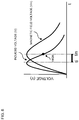
FIG. 7 ). - Meanwhile, in the rising pulse detection, tm is close to ti, and the induced voltage is significantly high at the time tm. Thus, the variation due to the magnetic field cannot be ignored (
FIG. 8 ). The present invention aims at removing the induced voltage from the output voltage of the GSR element and achieving a GSR sensor with a rising pulse detection system. - As a result of intensive study of the above-described technical problems, the inventors found that the polarity of an induced voltage becomes opposite relative to the direction of the current flowing in a magnetic wire. Then, they arrived at the technical idea of the present invention that if one coil includes therein two magnetic wires in which currents of opposite polarities flow, an induced voltage is cancelled, allowing for the detection of only a voltage in proportion to a magnetic field.
- Regarding the typical size of a coil in a GSR sensor element with one magnetic wire, the groove width is 20 µm, and the coil width is 40 µm. In the GSR sensor element with two magnetic wires, the groove width is 40 µm, in which two magnetic wires are arranged with a separation wall in the center, and the coil width is 50 µm. The size of the GSR sensor element is almost the same for one magnetic wire and for two magnetic wires.
- Three kinds of structures exist for the element.
- The first structure is a type in which two magnetic wires are arranged in a groove deeper than a magnetic wire, with the lower coil having a recessed shape and the upper coil having a plane surface shape. The second structure is a type in which two magnetic wires are arranged in a shallow groove of about half of the diameter of a magnetic wire, with the lower coil having a recessed shape and the upper coil having a convex shape.
- The third structure is a type in which a chevron-shaped guide is formed on a plane surface and each of the two magnetic wires is arranged in it, with the lower coil having a plane surface shape and the upper coil having a convex shape.
- In any kind of structure, a separation wall is provided between the two magnetic wires.
- The lower coil is arranged to deviate by a half pitch from the upper coil, and they are electrically connected on a joint surface thereof on the plane surface board to form a spiral coil. Each of two end parts of the coil is connected to two coil electrodes.
- Insulation between the magnetic wire and the coil is achieved by a method of adopting a magnetic wire coated with an insulating material, a method of inserting a magnetic wire in an insulating resist embedded in a groove, or a method combining both. To secure the insulation, it is preferable to use a magnetic wire coated with an insulating material.
- At the end part of the magnetic wire, a metal part of the magnetic wire is exposed from an insulating material and subject to wiring for electrical jointing to wire electrodes.
- The output of the GSR sensor element using two magnetic wires maintains excellent linearity even with the rising pulse detection for only a magnetic field voltage in proportion to a magnetic field.
- The output voltage of rising pulse detection is 2.5 times the output voltage of falling pulse detection. Furthermore, such a GSR sensor element has two magnetic wires, and thus it is possible to obtain output voltage that is 5 times greater. This indicates the possibility of downsizing the element because the number of windings of a coil N can be 1/5 and a coil length of the element can be 1/5.
- In addition, a pulse width of a pulse current can be a sufficiently long pulse width required for rising pulse detection, from 10ns to 1ns or less, for example. This reduces the power consumption of a pulse current to 1/10 or less.
- The GSR sensor ASIC includes a capacitor for storing power for pulse current transmission. The size of the capacitor occupies 50% of the ASIC. If the size of the capacitor can be reduced to 1/10, the size of the ASIC can be reduced to almost half.
- The GSR sensor element with two magnetic wires in one coil removes induced voltage components of the coil voltage to improve the linearity of an output voltage, which is dependent on a magnetic field, in rising pulse detection, increase sensitivity (output voltage per unit of magnetic field intensity of 1G) fivefold, and reduce the power consumption of a pulse current to 1/10 or less. In this manner, it is possible to downsize the element and the ASIC under the same conditions of output voltages.
-
-
FIG. 1 is a schematic diagram illustrating a front surface of a GSR sensor element according to an embodiment and an example; -
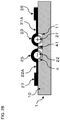
FIG. 2A is a sectional view illustrating the GSR sensor element viewed along the A1-A2 line ofFIG. 1 according to the embodiment; -
FIG. 2B is a sectional view illustrating the GSR sensor element viewed along the A3-A4 line ofFIG. 1 according to the embodiment; -
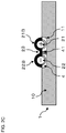
FIG. 2C is a sectional view illustrating the GSR sensor element viewed along the A5-A6 line ofFIG. 1 according to the embodiment; -
FIG. 3 is a sectional view illustrating another type (recessed shape) of the GSR sensor element according to the embodiment; -
FIG. 4 is a sectional view illustrating another type (convex shape) of the GSR sensor element according to the embodiment; -
FIG. 5 is a block circuit diagram illustrating an electronic circuit of the GSR sensor according to the example; -
FIG. 6 is a characteristic diagram illustrating the relation between an external magnetic field and an output voltage of the magnetic sensor in the GSR sensor according to the example and comparative examples; -
FIG. 7 is a progress diagram of the temporal change of a magnetic field voltage and an induced voltage in falling pulse detection; and -
FIG. 8 is a progress diagram of the temporal change of a magnetic field voltage and an induced voltage in rising pulse detection. - A
GSR sensor element 1 of the present embodiment includes, on anelectrode wiring board 10, a Co alloy magnetic wire 2 (21 and 22) coated with an insulating film, a coil 3 (31 and 32) wound around themagnetic wire 2, and four terminals (23 and 25, 34 and 36), as illustrated inFIG. 1 ,FIG. 2A ,FIG. 2B , andFIG. 2C . - As the
magnetic wire 2, there are arranged twomagnetic wires wall 41, in agroove 11 on a center part of a board. - The upper part of the
magnetic wire 21 on the wire input electrode 26(+) side, illustrated on the right side ofFIG. 1 , is connected to a wire input electrode 26(+) through thewire terminal 23 and a wire connection portion 21A (right part ofFIG. 2B ). - The lower part of the
magnetic wire 21 is connected to the lower part of themagnetic wire 22 on the wire output electrode 27(-) side through a wirejoint part 22B illustrated on the left side through a wirejoint part 21B and a wire connection portion 23 (FIG. 2C ). - The upper portion of the
magnetic wire 22 is connected to a wire output electrode 27(-) through the wire terminal 25 (left part ofFIG. 2B ). - Next, the
coil 3 includes alower coil 31, anupper coil 32, and ajoint part 33 jointing both coils. - The
lower coil 31 is formed in a recessed shape in thegroove 11 and on theboard 10, while theupper coil 32 is formed from the upper part of a pair ofmagnetic wires material 4 and then onto theboard 10. - The end part of the
lower coil 31 and the end part of theupper coil 32 form thejoint part 33 on theboard 10 to be connected to each other. - Note that the pair of magnetic wires 2 (21 and 22) are insulated from each other by the insulating
wall 41, and themagnetic wire 2 is insulated from thecoil 3 by the insulatingmaterial 4. - In this manner, a current flows downward in the
magnetic wire 21 on the right side, while a current flows upward in themagnetic wire 22 on the left side, whereby in one coil, the directions of currents are opposite from each other through the insulating material, which cancels an induced voltage. - In the present embodiment, a pair of magnetic wires formed of two magnetic wires is arranged in one coil so that the current directions thereof are opposite from each other through the insulating material. However, a plurality of pairs of magnetic wires may be arranged in one coil.
- Moreover, in the present embodiment, as the magnetic wire, there is used a magnetic wire coated with glass that is the insulating material. However, it is also possible to use a magnetic wire not coated with an insulating material.
- In the present embodiment, the structure of the element is of the type in which two magnetic wires (21 and 22) are arranged in the
shallow groove 11 of about half of the diameter of themagnetic wire 2, and thelower coil 31 has a recessed shape and theupper coil 32 has a convex shape, as illustrated inFIG. 2A . - As another type of structure, two magnetic wires (21 and 22) are arranged in the
groove 11 deeper than themagnetic wire 2, and thelower coil 31 has a recessed shape and theupper coil 32 has a plane surface shape, as illustrated inFIG. 3 . Moreover, the third type of structure is of the type in which a chevron-shaped guide is formed on a plane surface and each of the two magnetic wires (21 and 22) is arranged in it, and thelower coil 31 has a plane surface shape, and theupper coil 32 has a convex shape, as illustrated inFIG. 4 . - In any kind of structure, a separation wall is provided between the two magnetic wires (21 and 22). The
joint part 33 connecting the end part of thelower coil 31 and the end part of theupper coil 32 is provided to form thecoil 3. - The following will describe a method of manufacturing the GSR sensor element.
- For the
electrode wiring board 10, there is used a Si substrate coated with SiN. For themagnetic wire 2, there is used an amorphous wire having a diameter of 1 to 20 µm and a length of 0.07 to 1.0 mm coated with a glass insulating film. - First, in the
element 1 having a width of 0.25 mm, thegroove 11 with a width of 20 to 60 µm and a depth of 2 to 20 µm is formed in the center part thereof. - Next, electrode wiring is performed in the
lower coil 31 and on the board surface along thegroove 11. Then, the insulatingwall 41 is formed in the center part of thegroove 11 to have a two-groove form, and each one of the twomagnetic wires upper coil 32 is formed by photolithographic technology. - The
joint part 33 is formed to diagonally join the end parts of thelower coil 31 and theupper coil 32 on the board surface, so as to form thecoil 3 with a coil pitch of 2 to 10 µm. Acoil terminal 34 is connected to a coil output electrode 35(+), and acoil terminal 35 is connected to a coil ground electrode 37(-). - At the four ends of the two magnetic wires, the glass as an insulating film is removed. The
wire terminal 23 and the connection portion 21A are formed at one of the two ends by metal vapor deposition to enable electrical connection to a wire input electrode 26(+), while thewire terminal 25 and aconnection portion 22A are formed at the other end by metal vapor deposition to enable electrical connection to a wire ground electrode 27(-). - Then, the other two end parts are subjected to metal vapor deposition (21B and 22B), and a
connection portion 23 connecting the two end parts is formed by metal vapor deposition. - In this manner, the wiring for the power supply of a pulse current is performed from the wire input electrode 26(+) to the wire ground electrode 27(-).
- In the present embodiment, the output voltage exhibits sine wave output characteristics relative to a magnetic field H, and the linearity is 0.3% or lower in a measurement range of ±3 to 90G, which is excellent.
- The sensitivity is 50 to 2000 mV/G and is about five times higher than that of the GSR sensor element having the same length of magnetic wire.
- The pulse power consumption is 0.3 mW (0.15 mA).
- The following will describe the GSR sensor element according to an example of the present invention with reference to
FIG. 1 ,FIG. 5 , andFIG. 6 . - The
board 10 is formed of an Si substrate insulated and coated with SiN. The size of theboard 10 is 0.2 mm in length, 0.2 mm in width, and 0.2 mm in height. Themagnetic wire 2 is an amorphous wire of a CoFeSiB-based alloy having a diameter of 10 µm and has a length of 0.20 mm coated with glass. - The width of the
groove 11 of theboard 10 is 40 µm, and the depth thereof is 6 µm. The size of the insulatingwall 41 formed by an insulating resist in thegroove 11 has a width of 2 µm and a height of 6 µm. - The
coil 3 has a width of 50 µm, a height of 14 µm, and an average internal diameter (diameter of a circle equivalent to a sectional area in a coil formed by a height and a width) of 26 µm. The coil pitch is 5 µm, and the number of windings of the coil is 28. - Next, the characteristics of the
GSR sensor element 1 were evaluated using an electronic circuit for an MI sensor illustrated inFIG. 5 . - The
electronic circuit 5 includes apulse oscillator 51, theGSR sensor element 1, and asignal processing circuit 52 including abuffer circuit 53. The signal is a pulse signal with an intensity of 100mA equivalent to 1GHz, and inputs a pulse current with a rising time of 0.5 nsec, a pulse width of 1 nsec, and a falling time of 0.5 nsec. - The pulse signal is input to the
amorphous wire 2, and during the pulse applying operation, a voltage in proportion to the external magnetic field occurs in themagnetic coil 3, which is subject to rising pulse detection. - The
signal processing circuit 52 inputs the voltage occurred in thecoil 3 to thebuffer circuit 53, and the output from thebuffer circuit 53 is input to asample hold circuit 56 through anelectronic switch 55. The timing of opening and closing of theelectronic switch 55 is adjusted by a pulse detectiontiming adjustment circuit 54 to allow detection at a timing adequate for rising pulse signals, and the voltage at the time is sampled and held. Thereafter, the voltage is amplified to a given voltage by anamplifier 57. -
FIG. 6 illustrates sensor output from the electronic circuit. InFIG. 6 , the horizontal axis shows the intensity of an external magnetic field, and the vertical axis shows a sensor output voltage. - The sensor output exhibits sine wave output characteristics, and shows the linearity in a range of ±90G by arcsin conversion. The nonlinearity is 0.3%. The sensitivity is 210 mV/G.
- An MI element used for the product on the market AMI306 (length: 0.6 mm, width: 0.3 mm) as Comparative Example 1, and a GSR sensor element for vehicles (length: 0.15 mm, width: 0.20 mm) as Comparative Example 2 were subjected to measurement evaluation using the same electronic circuit. The results are illustrated by Comparative Examples 1 and 2 in
FIG. 6 . - Regarding the sensor output voltage at the magnetic field intensity of 90 Oe, the GSR sensor of the present invention obtains an excellent sensitivity of 1.5V relative to 0.1V in the MI sensor of Comparative Example 1 and 0.3V in the GSR sensor of Comparative Example 2.
- As described above, the GSR sensor element of the present invention is considerably compact in size and achieves high sensitivity. In this manner, the GSR sensor formed by the element achieves significantly high sensitivity, compactness in size, and low power consumption, and thus it can be embedded in catheters. Moreover, it can also be adapted to wider fields such as smartphones.
-
- 1 GSR sensor element plate
- 10 board
- 11 groove on a substrate
- 2 magnetic wire
- 21 one of a pair of magnetic wires
- 22 the other of a pair of magnetic wires
- 21A connection portion between wire terminal and wire input electrode(+)
- 22A connection portion between wire terminal and wire output electrode(-)
- 21B wire joint part
- 22B wire joint part
- 23 terminal of magnetic wire
- 24 connection portion between wires
- 25 terminal of magnetic wire
- 26 wire input electrode(+)
- 27 wire output electrode(-)
- 3 coil
- 31 lower coil
- 32 upper coil
- 33 joint part
- 4 insulating material
- 41 insulating wall
- 5 electronic circuit
- 51 pulse oscillator
- 52 signal processing circuit
- 53 buffer circuit
- 54 pulse detection timing adjustment circuit
- 55 electronic switch
- 56 sample hold circuit
- 57 amplifier
Claims (6)
- A GSR sensor element, comprising:an electrode wiring board;a magnetic wire that is a magnetosensitive body formed on the electrode wiring board;a coil wound around the magnetic wire;and four terminals formed on end parts of the coil for connection to an external integrated circuit, whereinthe coil includes a pair of the magnetic wires having currents flowing in opposite directions through an insulating material,the coil includes a coil lower part, a coil upper part, and a joint part connecting both, andthe pair of the magnetic wires are separated by an insulating wall in the coil.
- The GSR sensor element according to claim 1, wherein the magnetic wire includes a plurality of pairs of magnetic wires.
- The GSR sensor element according to claim 1, wherein an outer periphery of the magnetic wire is coated with an insulating material.
- The GSR sensor element according to claim 1, wherein
the coil includes a recessed coil lower part, a convex coil upper part, and the joint part connecting both,
the pair of the magnetic wires are embedded in a groove on the board coated with an insulating material and are subjected to wiring at the coil lower part and fixed by insulating resin having an adhesion function and a resist function,
an upper part of the pair of the magnetic wires is covered thinly by surface tension of the insulating resin and subjected to wiring at the coil upper part, and
the joint part electrically joints an end part of the coil lower part and an end part of the coil upper part to form a coil. - The GSR sensor element according to claim 1, wherein
the coil includes a recessed coil lower part, a plane coil upper part, and the joint part connecting both,
the pair of the magnetic wires are inserted in a groove on the board having an embedded insulating material and are subjected to wiring at the coil lower part,
an upper surface of the groove is subjected to wiring at the coil upper part, and
the joint part electrically joints an end part of the coil lower part and an end part of the coil upper part to form a coil. - The GSR sensor element according to claim 1, wherein
the coil includes a plane coil lower part, a convex coil upper part, and the joint part connecting both,
the pair of the magnetic wires are fixed by insulating resin on an upper surface of wiring at the coil lower part performed on a flat surface of the board,
a side part and an upper part of the pair of the magnetic wires are covered thinly by insulating resin and are subjected to wiring at the coil upper part, and
the joint part electrically joints an end part of the coil lower part and an end part of the coil upper part to form a coil.
Applications Claiming Priority (2)
| Application Number | Priority Date | Filing Date | Title |
|---|---|---|---|
| JP2017110509A JP6864413B2 (en) | 2017-06-05 | 2017-06-05 | GSR sensor element |
| PCT/JP2018/018555 WO2018225454A1 (en) | 2017-06-05 | 2018-05-14 | Gsr sensor element |
Publications (3)
| Publication Number | Publication Date |
|---|---|
| EP3637122A1 true EP3637122A1 (en) | 2020-04-15 |
| EP3637122A4 EP3637122A4 (en) | 2020-11-11 |
| EP3637122B1 EP3637122B1 (en) | 2024-01-03 |
Family
ID=64566622
Family Applications (1)
| Application Number | Title | Priority Date | Filing Date |
|---|---|---|---|
| EP18813629.5A Active EP3637122B1 (en) | 2017-06-05 | 2018-05-14 | Gsr sensor element |
Country Status (13)
| Country | Link |
|---|---|
| US (1) | US11156676B2 (en) |
| EP (1) | EP3637122B1 (en) |
| JP (1) | JP6864413B2 (en) |
| KR (2) | KR20200014263A (en) |
| CN (1) | CN110073231B (en) |
| AU (2) | AU2018281459A1 (en) |
| BR (1) | BR112019012644B1 (en) |
| CA (1) | CA3047546C (en) |
| IL (1) | IL267588B2 (en) |
| MX (1) | MX2019007321A (en) |
| MY (1) | MY202561A (en) |
| RU (1) | RU2726269C1 (en) |
| WO (1) | WO2018225454A1 (en) |
Families Citing this family (10)
| Publication number | Priority date | Publication date | Assignee | Title |
|---|---|---|---|---|
| JP7262885B2 (en) * | 2017-06-16 | 2023-04-24 | 朝日インテック株式会社 | Ultra-sensitive micro magnetic sensor |
| JP7262886B2 (en) * | 2017-07-21 | 2023-04-24 | 朝日インテック株式会社 | Ultra-compact high-sensitivity magnetic sensor |
| WO2021100252A1 (en) * | 2019-11-22 | 2021-05-27 | Tdk株式会社 | Magnetic sensor |
| JP2022006490A (en) * | 2020-06-24 | 2022-01-13 | 朝日インテック株式会社 | Medical system and image generation method |
| JP6839399B1 (en) * | 2020-09-29 | 2021-03-10 | マグネデザイン株式会社 | Magnetic field detection element |
| CN116034648A (en) * | 2020-09-30 | 2023-04-28 | 爱知制钢株式会社 | Magneto-impedance sensor element |
| JP7203400B1 (en) | 2022-10-17 | 2023-01-13 | マグネデザイン株式会社 | Method for manufacturing GSR element |
| JP7201194B1 (en) | 2022-10-17 | 2023-01-10 | マグネデザイン株式会社 | Method for manufacturing magnetic field detection element |
| JP7207676B1 (en) | 2022-10-17 | 2023-01-18 | マグネデザイン株式会社 | Method for manufacturing GSR element |
| WO2024085098A1 (en) * | 2022-10-17 | 2024-04-25 | マグネデザイン株式会社 | Gsr element manufacturing method |
Family Cites Families (31)
| Publication number | Priority date | Publication date | Assignee | Title |
|---|---|---|---|---|
| JPS5839527B2 (en) | 1977-04-20 | 1983-08-30 | 東京光学機械株式会社 | Remote optometry device |
| JPS5839527U (en) | 1981-09-10 | 1983-03-15 | 井関農機株式会社 | Weighing device in fruit sorting machine |
| JPH0360357A (en) * | 1989-07-27 | 1991-03-15 | Nippon Steel Corp | Low inductance actuator |
| JPH07120436A (en) * | 1993-10-20 | 1995-05-12 | Seiko Instr Inc | Non-destructive inspection device |
| JP4007464B2 (en) * | 1997-10-06 | 2007-11-14 | Tdk株式会社 | Magnetic detector |
| JP2001052947A (en) * | 1999-08-09 | 2001-02-23 | Sony Corp | Coil, electromagnet and manufacturing method |
| RU39718U1 (en) * | 2004-03-29 | 2004-08-10 | Государственное образовательное учреждение высшего профессионального образования "Омский государственный университет" | SQUID MAGNETOMETER - GRADIOMETER |
| JP4732705B2 (en) * | 2004-04-30 | 2011-07-27 | 独立行政法人科学技術振興機構 | Magnetic field sensor |
| JP4529783B2 (en) * | 2005-04-25 | 2010-08-25 | 愛知製鋼株式会社 | Magnet impedance sensor element |
| JP2008275578A (en) | 2007-04-05 | 2008-11-13 | Fujikura Ltd | Magnetic sensor and manufacturing method thereof |
| JP4655162B2 (en) * | 2007-10-02 | 2011-03-23 | 愛知製鋼株式会社 | Magneto-impedance element and magneto-impedance sensor |
| JP4725600B2 (en) * | 2008-06-10 | 2011-07-13 | 愛知製鋼株式会社 | Magneto impedance sensor element |
| US8237438B2 (en) * | 2009-03-13 | 2012-08-07 | Quantec Geoscience | Very low noise magnetometer |
| CN201392201Y (en) * | 2009-03-31 | 2010-01-27 | 锦州北方航海仪器有限公司 | Planar sensor for ship log |
| JP5110142B2 (en) * | 2010-10-01 | 2012-12-26 | 愛知製鋼株式会社 | Magnetoimpedance sensor element and manufacturing method thereof |
| CN102283656A (en) * | 2011-05-23 | 2011-12-21 | 中国人民解放军空军航空医学研究所 | Integrated PPG (photoplethysmography) and GSR (galvanicskin response) signal sensor structure |
| JP5815353B2 (en) * | 2011-09-28 | 2015-11-17 | 株式会社フジクラ | Coil wiring element and method of manufacturing coil wiring element |
| WO2013047367A1 (en) | 2011-09-28 | 2013-04-04 | シャープ株式会社 | Display device and television receiving device |
| JP5747194B2 (en) * | 2012-02-24 | 2015-07-08 | サイレックス・テクノロジー株式会社 | Wireless access point with high connectivity and its program |
| CN103791921B (en) * | 2012-10-29 | 2016-10-12 | 北京嘉岳同乐极电子有限公司 | A kind of Magnetic Sensor and preparation method thereof |
| JP5747294B1 (en) * | 2013-08-20 | 2015-07-15 | マグネデザイン株式会社 | Magnet impedance sensor element with electromagnetic coil and magneto impedance sensor with electromagnetic coil |
| US9383418B2 (en) * | 2014-05-23 | 2016-07-05 | Texas Instruments Incorporated | Integrated dual axis fluxgate sensor using double deposition of magnetic material |
| JP6483435B2 (en) * | 2014-12-26 | 2019-03-13 | ローム株式会社 | Magnetic detector |
| CN104569870B (en) * | 2015-01-07 | 2017-07-21 | 江苏多维科技有限公司 | A kind of single-chip has the z axis magnetic resistance sensor of calibration/replacement coil |
| JP5839527B1 (en) * | 2015-02-16 | 2016-01-06 | マグネデザイン株式会社 | Ultra-sensitive micro magnetic sensor |
| US10371763B2 (en) * | 2015-07-17 | 2019-08-06 | Honeywell International Inc. | Systems and methods for low power magnetic field generation for atomic sensors using electro-permanent magnets |
| TWI545332B (en) | 2015-09-10 | 2016-08-11 | 旺玖科技股份有限公司 | Magneto-impedance sensor device and method for fafbicating the same |
| JP6766333B2 (en) * | 2015-10-06 | 2020-10-14 | 愛知製鋼株式会社 | Micromagnetic material detection sensor and foreign matter detection device |
| JP6021238B1 (en) * | 2015-10-11 | 2016-11-09 | マグネデザイン株式会社 | Gradio sensor element and gradio sensor |
| JP5991634B1 (en) * | 2015-12-18 | 2016-09-14 | マグネデザイン株式会社 | Magnetic detector |
| CN105911487B (en) * | 2016-04-14 | 2018-12-14 | 中国科学院上海微系统与信息技术研究所 | A kind of superconducting magnetic sensor search coil and detector |
-
2017
- 2017-06-05 JP JP2017110509A patent/JP6864413B2/en active Active
-
2018
- 2018-05-14 KR KR1020197025478A patent/KR20200014263A/en not_active Ceased
- 2018-05-14 CN CN201880004843.5A patent/CN110073231B/en active Active
- 2018-05-14 CA CA3047546A patent/CA3047546C/en active Active
- 2018-05-14 BR BR112019012644-9A patent/BR112019012644B1/en active IP Right Grant
- 2018-05-14 WO PCT/JP2018/018555 patent/WO2018225454A1/en not_active Ceased
- 2018-05-14 MY MYPI2019003514A patent/MY202561A/en unknown
- 2018-05-14 MX MX2019007321A patent/MX2019007321A/en unknown
- 2018-05-14 AU AU2018281459A patent/AU2018281459A1/en not_active Abandoned
- 2018-05-14 KR KR1020237023043A patent/KR102702021B1/en active Active
- 2018-05-14 RU RU2019117618A patent/RU2726269C1/en active
- 2018-05-14 EP EP18813629.5A patent/EP3637122B1/en active Active
-
2019
- 2019-06-14 US US16/441,040 patent/US11156676B2/en active Active
- 2019-06-23 IL IL267588A patent/IL267588B2/en unknown
-
2021
- 2021-03-09 AU AU2021201488A patent/AU2021201488B2/en active Active
Also Published As
| Publication number | Publication date |
|---|---|
| IL267588B1 (en) | 2023-01-01 |
| IL267588A (en) | 2019-11-28 |
| BR112019012644B1 (en) | 2023-12-26 |
| AU2021201488B2 (en) | 2023-03-23 |
| KR102702021B1 (en) | 2024-09-04 |
| CN110073231A (en) | 2019-07-30 |
| IL267588B2 (en) | 2023-05-01 |
| KR20200014263A (en) | 2020-02-10 |
| WO2018225454A1 (en) | 2018-12-13 |
| EP3637122A4 (en) | 2020-11-11 |
| CN110073231B (en) | 2021-11-19 |
| EP3637122B1 (en) | 2024-01-03 |
| AU2018281459A1 (en) | 2019-07-11 |
| CA3047546C (en) | 2022-09-27 |
| MX2019007321A (en) | 2020-02-07 |
| CA3047546A1 (en) | 2018-12-13 |
| BR112019012644A2 (en) | 2019-11-19 |
| US20190302195A1 (en) | 2019-10-03 |
| MY202561A (en) | 2024-05-08 |
| AU2021201488A1 (en) | 2021-03-25 |
| KR20230107904A (en) | 2023-07-18 |
| US11156676B2 (en) | 2021-10-26 |
| JP2018205102A (en) | 2018-12-27 |
| RU2726269C1 (en) | 2020-07-10 |
| JP6864413B2 (en) | 2021-04-28 |
Similar Documents
| Publication | Publication Date | Title |
|---|---|---|
| AU2021201488B2 (en) | GSR sensor element | |
| US20160116551A1 (en) | Magneto-impedance sensor element with electromagnetic coil and magneto-impedance sensor with electromagnetic coil | |
| DE19514342C1 (en) | Radio-interrogated current transducer for HV or MV appts. | |
| AU2018284779B2 (en) | Ultra high-sensitivity micro magnetic sensor | |
| CN101815953B (en) | Magneto-impedance element and magneto-impedance sensor | |
| TWI259284B (en) | Magnet, impedance and sensor device having electromagnetic coil | |
| EP3657192A1 (en) | Ultra-small high-sensitivity magnetic sensor | |
| WO2010043433A1 (en) | Device for measuring the direction and/or strength of a magnetic field | |
| JP7062216B2 (en) | Ultra-thin high-sensitivity magnetic sensor | |
| EP0632897B1 (en) | Inductive sensor | |
| JPS63302371A (en) | Current detector | |
| US11486904B2 (en) | Electronic module | |
| JP2020003370A (en) | Small three-dimensional magnetic field detector |
Legal Events
| Date | Code | Title | Description |
|---|---|---|---|
| STAA | Information on the status of an ep patent application or granted ep patent |
Free format text: STATUS: THE INTERNATIONAL PUBLICATION HAS BEEN MADE |
|
| PUAI | Public reference made under article 153(3) epc to a published international application that has entered the european phase |
Free format text: ORIGINAL CODE: 0009012 |
|
| STAA | Information on the status of an ep patent application or granted ep patent |
Free format text: STATUS: REQUEST FOR EXAMINATION WAS MADE |
|
| 17P | Request for examination filed |
Effective date: 20190617 |
|
| AK | Designated contracting states |
Kind code of ref document: A1 Designated state(s): AL AT BE BG CH CY CZ DE DK EE ES FI FR GB GR HR HU IE IS IT LI LT LU LV MC MK MT NL NO PL PT RO RS SE SI SK SM TR |
|
| AX | Request for extension of the european patent |
Extension state: BA ME |
|
| DAV | Request for validation of the european patent (deleted) | ||
| DAX | Request for extension of the european patent (deleted) | ||
| REG | Reference to a national code |
Ref country code: DE Ref legal event code: R079 Free format text: PREVIOUS MAIN CLASS: G01R0033020000 Ipc: G01R0033060000 Ref document number: 602018063693 Country of ref document: DE |
|
| A4 | Supplementary search report drawn up and despatched |
Effective date: 20201008 |
|
| RIC1 | Information provided on ipc code assigned before grant |
Ipc: G01R 33/06 20060101AFI20201005BHEP Ipc: A61B 5/06 20060101ALI20201005BHEP |
|
| STAA | Information on the status of an ep patent application or granted ep patent |
Free format text: STATUS: EXAMINATION IS IN PROGRESS |
|
| 17Q | First examination report despatched |
Effective date: 20230113 |
|
| GRAP | Despatch of communication of intention to grant a patent |
Free format text: ORIGINAL CODE: EPIDOSNIGR1 |
|
| STAA | Information on the status of an ep patent application or granted ep patent |
Free format text: STATUS: GRANT OF PATENT IS INTENDED |
|
| INTG | Intention to grant announced |
Effective date: 20230718 |
|
| RIN1 | Information on inventor provided before grant (corrected) |
Inventor name: HONKURA, SHINPEI Inventor name: TANABE, JUNICHI Inventor name: KUDO, KAZUE Inventor name: KIKUCHI, EIKI Inventor name: HONKURA, YOSHINOBU |
|
| GRAS | Grant fee paid |
Free format text: ORIGINAL CODE: EPIDOSNIGR3 |
|
| GRAA | (expected) grant |
Free format text: ORIGINAL CODE: 0009210 |
|
| STAA | Information on the status of an ep patent application or granted ep patent |
Free format text: STATUS: THE PATENT HAS BEEN GRANTED |
|
| AK | Designated contracting states |
Kind code of ref document: B1 Designated state(s): AL AT BE BG CH CY CZ DE DK EE ES FI FR GB GR HR HU IE IS IT LI LT LU LV MC MK MT NL NO PL PT RO RS SE SI SK SM TR |
|
| RAP3 | Party data changed (applicant data changed or rights of an application transferred) |
Owner name: ASAHI INTECC CO., LTD. |
|
| REG | Reference to a national code |
Ref country code: GB Ref legal event code: FG4D |
|
| REG | Reference to a national code |
Ref country code: CH Ref legal event code: EP |
|
| REG | Reference to a national code |
Ref country code: DE Ref legal event code: R096 Ref document number: 602018063693 Country of ref document: DE |
|
| REG | Reference to a national code |
Ref country code: IE Ref legal event code: FG4D |
|
| REG | Reference to a national code |
Ref country code: LT Ref legal event code: MG9D |
|
| PG25 | Lapsed in a contracting state [announced via postgrant information from national office to epo] |
Ref country code: ES Free format text: LAPSE BECAUSE OF FAILURE TO SUBMIT A TRANSLATION OF THE DESCRIPTION OR TO PAY THE FEE WITHIN THE PRESCRIBED TIME-LIMIT Effective date: 20240103 |
|
| PG25 | Lapsed in a contracting state [announced via postgrant information from national office to epo] |
Ref country code: ES Free format text: LAPSE BECAUSE OF FAILURE TO SUBMIT A TRANSLATION OF THE DESCRIPTION OR TO PAY THE FEE WITHIN THE PRESCRIBED TIME-LIMIT Effective date: 20240103 |
|
| REG | Reference to a national code |
Ref country code: NL Ref legal event code: MP Effective date: 20240103 |
|
| REG | Reference to a national code |
Ref country code: AT Ref legal event code: MK05 Ref document number: 1647323 Country of ref document: AT Kind code of ref document: T Effective date: 20240103 |
|
| PG25 | Lapsed in a contracting state [announced via postgrant information from national office to epo] |
Ref country code: NL Free format text: LAPSE BECAUSE OF FAILURE TO SUBMIT A TRANSLATION OF THE DESCRIPTION OR TO PAY THE FEE WITHIN THE PRESCRIBED TIME-LIMIT Effective date: 20240103 |
|
| PG25 | Lapsed in a contracting state [announced via postgrant information from national office to epo] |
Ref country code: NL Free format text: LAPSE BECAUSE OF FAILURE TO SUBMIT A TRANSLATION OF THE DESCRIPTION OR TO PAY THE FEE WITHIN THE PRESCRIBED TIME-LIMIT Effective date: 20240103 |
|
| PG25 | Lapsed in a contracting state [announced via postgrant information from national office to epo] |
Ref country code: IS Free format text: LAPSE BECAUSE OF FAILURE TO SUBMIT A TRANSLATION OF THE DESCRIPTION OR TO PAY THE FEE WITHIN THE PRESCRIBED TIME-LIMIT Effective date: 20240503 |
|
| PG25 | Lapsed in a contracting state [announced via postgrant information from national office to epo] |
Ref country code: LT Free format text: LAPSE BECAUSE OF FAILURE TO SUBMIT A TRANSLATION OF THE DESCRIPTION OR TO PAY THE FEE WITHIN THE PRESCRIBED TIME-LIMIT Effective date: 20240103 |
|
| PG25 | Lapsed in a contracting state [announced via postgrant information from national office to epo] |
Ref country code: GR Free format text: LAPSE BECAUSE OF FAILURE TO SUBMIT A TRANSLATION OF THE DESCRIPTION OR TO PAY THE FEE WITHIN THE PRESCRIBED TIME-LIMIT Effective date: 20240404 |
|
| PG25 | Lapsed in a contracting state [announced via postgrant information from national office to epo] |
Ref country code: RS Free format text: LAPSE BECAUSE OF FAILURE TO SUBMIT A TRANSLATION OF THE DESCRIPTION OR TO PAY THE FEE WITHIN THE PRESCRIBED TIME-LIMIT Effective date: 20240403 Ref country code: HR Free format text: LAPSE BECAUSE OF FAILURE TO SUBMIT A TRANSLATION OF THE DESCRIPTION OR TO PAY THE FEE WITHIN THE PRESCRIBED TIME-LIMIT Effective date: 20240103 |
|
| PG25 | Lapsed in a contracting state [announced via postgrant information from national office to epo] |
Ref country code: AT Free format text: LAPSE BECAUSE OF FAILURE TO SUBMIT A TRANSLATION OF THE DESCRIPTION OR TO PAY THE FEE WITHIN THE PRESCRIBED TIME-LIMIT Effective date: 20240103 Ref country code: CZ Free format text: LAPSE BECAUSE OF FAILURE TO SUBMIT A TRANSLATION OF THE DESCRIPTION OR TO PAY THE FEE WITHIN THE PRESCRIBED TIME-LIMIT Effective date: 20240103 |
|
| PG25 | Lapsed in a contracting state [announced via postgrant information from national office to epo] |
Ref country code: RS Free format text: LAPSE BECAUSE OF FAILURE TO SUBMIT A TRANSLATION OF THE DESCRIPTION OR TO PAY THE FEE WITHIN THE PRESCRIBED TIME-LIMIT Effective date: 20240403 Ref country code: NO Free format text: LAPSE BECAUSE OF FAILURE TO SUBMIT A TRANSLATION OF THE DESCRIPTION OR TO PAY THE FEE WITHIN THE PRESCRIBED TIME-LIMIT Effective date: 20240403 Ref country code: LT Free format text: LAPSE BECAUSE OF FAILURE TO SUBMIT A TRANSLATION OF THE DESCRIPTION OR TO PAY THE FEE WITHIN THE PRESCRIBED TIME-LIMIT Effective date: 20240103 Ref country code: IS Free format text: LAPSE BECAUSE OF FAILURE TO SUBMIT A TRANSLATION OF THE DESCRIPTION OR TO PAY THE FEE WITHIN THE PRESCRIBED TIME-LIMIT Effective date: 20240503 Ref country code: HR Free format text: LAPSE BECAUSE OF FAILURE TO SUBMIT A TRANSLATION OF THE DESCRIPTION OR TO PAY THE FEE WITHIN THE PRESCRIBED TIME-LIMIT Effective date: 20240103 Ref country code: GR Free format text: LAPSE BECAUSE OF FAILURE TO SUBMIT A TRANSLATION OF THE DESCRIPTION OR TO PAY THE FEE WITHIN THE PRESCRIBED TIME-LIMIT Effective date: 20240404 Ref country code: CZ Free format text: LAPSE BECAUSE OF FAILURE TO SUBMIT A TRANSLATION OF THE DESCRIPTION OR TO PAY THE FEE WITHIN THE PRESCRIBED TIME-LIMIT Effective date: 20240103 Ref country code: BG Free format text: LAPSE BECAUSE OF FAILURE TO SUBMIT A TRANSLATION OF THE DESCRIPTION OR TO PAY THE FEE WITHIN THE PRESCRIBED TIME-LIMIT Effective date: 20240103 Ref country code: AT Free format text: LAPSE BECAUSE OF FAILURE TO SUBMIT A TRANSLATION OF THE DESCRIPTION OR TO PAY THE FEE WITHIN THE PRESCRIBED TIME-LIMIT Effective date: 20240103 |
|
| PG25 | Lapsed in a contracting state [announced via postgrant information from national office to epo] |
Ref country code: PL Free format text: LAPSE BECAUSE OF FAILURE TO SUBMIT A TRANSLATION OF THE DESCRIPTION OR TO PAY THE FEE WITHIN THE PRESCRIBED TIME-LIMIT Effective date: 20240103 Ref country code: PT Free format text: LAPSE BECAUSE OF FAILURE TO SUBMIT A TRANSLATION OF THE DESCRIPTION OR TO PAY THE FEE WITHIN THE PRESCRIBED TIME-LIMIT Effective date: 20240503 |
|
| PG25 | Lapsed in a contracting state [announced via postgrant information from national office to epo] |
Ref country code: SE Free format text: LAPSE BECAUSE OF FAILURE TO SUBMIT A TRANSLATION OF THE DESCRIPTION OR TO PAY THE FEE WITHIN THE PRESCRIBED TIME-LIMIT Effective date: 20240103 Ref country code: PT Free format text: LAPSE BECAUSE OF FAILURE TO SUBMIT A TRANSLATION OF THE DESCRIPTION OR TO PAY THE FEE WITHIN THE PRESCRIBED TIME-LIMIT Effective date: 20240503 Ref country code: PL Free format text: LAPSE BECAUSE OF FAILURE TO SUBMIT A TRANSLATION OF THE DESCRIPTION OR TO PAY THE FEE WITHIN THE PRESCRIBED TIME-LIMIT Effective date: 20240103 Ref country code: LV Free format text: LAPSE BECAUSE OF FAILURE TO SUBMIT A TRANSLATION OF THE DESCRIPTION OR TO PAY THE FEE WITHIN THE PRESCRIBED TIME-LIMIT Effective date: 20240103 |
|
| REG | Reference to a national code |
Ref country code: DE Ref legal event code: R097 Ref document number: 602018063693 Country of ref document: DE |
|
| PG25 | Lapsed in a contracting state [announced via postgrant information from national office to epo] |
Ref country code: DK Free format text: LAPSE BECAUSE OF FAILURE TO SUBMIT A TRANSLATION OF THE DESCRIPTION OR TO PAY THE FEE WITHIN THE PRESCRIBED TIME-LIMIT Effective date: 20240103 |
|
| PG25 | Lapsed in a contracting state [announced via postgrant information from national office to epo] |
Ref country code: SM Free format text: LAPSE BECAUSE OF FAILURE TO SUBMIT A TRANSLATION OF THE DESCRIPTION OR TO PAY THE FEE WITHIN THE PRESCRIBED TIME-LIMIT Effective date: 20240103 |
|
| PG25 | Lapsed in a contracting state [announced via postgrant information from national office to epo] |
Ref country code: EE Free format text: LAPSE BECAUSE OF FAILURE TO SUBMIT A TRANSLATION OF THE DESCRIPTION OR TO PAY THE FEE WITHIN THE PRESCRIBED TIME-LIMIT Effective date: 20240103 |
|
| PG25 | Lapsed in a contracting state [announced via postgrant information from national office to epo] |
Ref country code: SK Free format text: LAPSE BECAUSE OF FAILURE TO SUBMIT A TRANSLATION OF THE DESCRIPTION OR TO PAY THE FEE WITHIN THE PRESCRIBED TIME-LIMIT Effective date: 20240103 |
|
| PG25 | Lapsed in a contracting state [announced via postgrant information from national office to epo] |
Ref country code: SM Free format text: LAPSE BECAUSE OF FAILURE TO SUBMIT A TRANSLATION OF THE DESCRIPTION OR TO PAY THE FEE WITHIN THE PRESCRIBED TIME-LIMIT Effective date: 20240103 Ref country code: SK Free format text: LAPSE BECAUSE OF FAILURE TO SUBMIT A TRANSLATION OF THE DESCRIPTION OR TO PAY THE FEE WITHIN THE PRESCRIBED TIME-LIMIT Effective date: 20240103 Ref country code: RO Free format text: LAPSE BECAUSE OF FAILURE TO SUBMIT A TRANSLATION OF THE DESCRIPTION OR TO PAY THE FEE WITHIN THE PRESCRIBED TIME-LIMIT Effective date: 20240103 Ref country code: EE Free format text: LAPSE BECAUSE OF FAILURE TO SUBMIT A TRANSLATION OF THE DESCRIPTION OR TO PAY THE FEE WITHIN THE PRESCRIBED TIME-LIMIT Effective date: 20240103 Ref country code: DK Free format text: LAPSE BECAUSE OF FAILURE TO SUBMIT A TRANSLATION OF THE DESCRIPTION OR TO PAY THE FEE WITHIN THE PRESCRIBED TIME-LIMIT Effective date: 20240103 |
|
| PLBE | No opposition filed within time limit |
Free format text: ORIGINAL CODE: 0009261 |
|
| STAA | Information on the status of an ep patent application or granted ep patent |
Free format text: STATUS: NO OPPOSITION FILED WITHIN TIME LIMIT |
|
| PG25 | Lapsed in a contracting state [announced via postgrant information from national office to epo] |
Ref country code: IT Free format text: LAPSE BECAUSE OF FAILURE TO SUBMIT A TRANSLATION OF THE DESCRIPTION OR TO PAY THE FEE WITHIN THE PRESCRIBED TIME-LIMIT Effective date: 20240103 |
|
| 26N | No opposition filed |
Effective date: 20241007 |
|
| REG | Reference to a national code |
Ref country code: CH Ref legal event code: PL |
|
| PG25 | Lapsed in a contracting state [announced via postgrant information from national office to epo] |
Ref country code: IT Free format text: LAPSE BECAUSE OF FAILURE TO SUBMIT A TRANSLATION OF THE DESCRIPTION OR TO PAY THE FEE WITHIN THE PRESCRIBED TIME-LIMIT Effective date: 20240103 |
|
| PG25 | Lapsed in a contracting state [announced via postgrant information from national office to epo] |
Ref country code: MC Free format text: LAPSE BECAUSE OF FAILURE TO SUBMIT A TRANSLATION OF THE DESCRIPTION OR TO PAY THE FEE WITHIN THE PRESCRIBED TIME-LIMIT Effective date: 20240103 |
|
| PG25 | Lapsed in a contracting state [announced via postgrant information from national office to epo] |
Ref country code: LU Free format text: LAPSE BECAUSE OF NON-PAYMENT OF DUE FEES Effective date: 20240514 |
|
| PG25 | Lapsed in a contracting state [announced via postgrant information from national office to epo] |
Ref country code: MC Free format text: LAPSE BECAUSE OF FAILURE TO SUBMIT A TRANSLATION OF THE DESCRIPTION OR TO PAY THE FEE WITHIN THE PRESCRIBED TIME-LIMIT Effective date: 20240103 Ref country code: LU Free format text: LAPSE BECAUSE OF NON-PAYMENT OF DUE FEES Effective date: 20240514 Ref country code: CH Free format text: LAPSE BECAUSE OF NON-PAYMENT OF DUE FEES Effective date: 20240531 |
|
| REG | Reference to a national code |
Ref country code: BE Ref legal event code: MM Effective date: 20240531 |
|
| PG25 | Lapsed in a contracting state [announced via postgrant information from national office to epo] |
Ref country code: IE Free format text: LAPSE BECAUSE OF NON-PAYMENT OF DUE FEES Effective date: 20240514 |
|
| PG25 | Lapsed in a contracting state [announced via postgrant information from national office to epo] |
Ref country code: BE Free format text: LAPSE BECAUSE OF NON-PAYMENT OF DUE FEES Effective date: 20240531 Ref country code: SI Free format text: LAPSE BECAUSE OF FAILURE TO SUBMIT A TRANSLATION OF THE DESCRIPTION OR TO PAY THE FEE WITHIN THE PRESCRIBED TIME-LIMIT Effective date: 20240103 |
|
| PGFP | Annual fee paid to national office [announced via postgrant information from national office to epo] |
Ref country code: DE Payment date: 20250521 Year of fee payment: 8 |
|
| PGFP | Annual fee paid to national office [announced via postgrant information from national office to epo] |
Ref country code: FR Payment date: 20250528 Year of fee payment: 8 |
|
| PG25 | Lapsed in a contracting state [announced via postgrant information from national office to epo] |
Ref country code: CY Free format text: LAPSE BECAUSE OF FAILURE TO SUBMIT A TRANSLATION OF THE DESCRIPTION OR TO PAY THE FEE WITHIN THE PRESCRIBED TIME-LIMIT; INVALID AB INITIO Effective date: 20180514 |
|
| PG25 | Lapsed in a contracting state [announced via postgrant information from national office to epo] |
Ref country code: HU Free format text: LAPSE BECAUSE OF FAILURE TO SUBMIT A TRANSLATION OF THE DESCRIPTION OR TO PAY THE FEE WITHIN THE PRESCRIBED TIME-LIMIT; INVALID AB INITIO Effective date: 20180514 |
|
| PG25 | Lapsed in a contracting state [announced via postgrant information from national office to epo] |
Ref country code: FI Free format text: LAPSE BECAUSE OF FAILURE TO SUBMIT A TRANSLATION OF THE DESCRIPTION OR TO PAY THE FEE WITHIN THE PRESCRIBED TIME-LIMIT Effective date: 20240103 |
|
| PGFP | Annual fee paid to national office [announced via postgrant information from national office to epo] |
Ref country code: GB Payment date: 20260306 Year of fee payment: 9 |