EP3637113A1 - Current sensing device - Google Patents
Current sensing device Download PDFInfo
- Publication number
- EP3637113A1 EP3637113A1 EP18813198.1A EP18813198A EP3637113A1 EP 3637113 A1 EP3637113 A1 EP 3637113A1 EP 18813198 A EP18813198 A EP 18813198A EP 3637113 A1 EP3637113 A1 EP 3637113A1
- Authority
- EP
- European Patent Office
- Prior art keywords
- current
- core
- circuit
- sensing device
- coil
- Prior art date
- Legal status (The legal status is an assumption and is not a legal conclusion. Google has not performed a legal analysis and makes no representation as to the accuracy of the status listed.)
- Withdrawn
Links
Images




Classifications
-
- G—PHYSICS
- G01—MEASURING; TESTING
- G01R—MEASURING ELECTRIC VARIABLES; MEASURING MAGNETIC VARIABLES
- G01R15/00—Details of measuring arrangements of the types provided for in groups G01R17/00 - G01R29/00, G01R33/00 - G01R33/26 or G01R35/00
- G01R15/14—Adaptations providing voltage or current isolation, e.g. for high-voltage or high-current networks
- G01R15/18—Adaptations providing voltage or current isolation, e.g. for high-voltage or high-current networks using inductive devices, e.g. transformers
- G01R15/186—Adaptations providing voltage or current isolation, e.g. for high-voltage or high-current networks using inductive devices, e.g. transformers using current transformers with a core consisting of two or more parts, e.g. clamp-on type
-
- G—PHYSICS
- G01—MEASURING; TESTING
- G01R—MEASURING ELECTRIC VARIABLES; MEASURING MAGNETIC VARIABLES
- G01R15/00—Details of measuring arrangements of the types provided for in groups G01R17/00 - G01R29/00, G01R33/00 - G01R33/26 or G01R35/00
- G01R15/14—Adaptations providing voltage or current isolation, e.g. for high-voltage or high-current networks
- G01R15/18—Adaptations providing voltage or current isolation, e.g. for high-voltage or high-current networks using inductive devices, e.g. transformers
- G01R15/183—Adaptations providing voltage or current isolation, e.g. for high-voltage or high-current networks using inductive devices, e.g. transformers using transformers with a magnetic core
- G01R15/185—Adaptations providing voltage or current isolation, e.g. for high-voltage or high-current networks using inductive devices, e.g. transformers using transformers with a magnetic core with compensation or feedback windings or interacting coils, e.g. 0-flux sensors
-
- G—PHYSICS
- G01—MEASURING; TESTING
- G01R—MEASURING ELECTRIC VARIABLES; MEASURING MAGNETIC VARIABLES
- G01R19/00—Arrangements for measuring currents or voltages or for indicating presence or sign thereof
- G01R19/25—Arrangements for measuring currents or voltages or for indicating presence or sign thereof using digital measurement techniques
-
- H—ELECTRICITY
- H05—ELECTRIC TECHNIQUES NOT OTHERWISE PROVIDED FOR
- H05K—PRINTED CIRCUITS; CASINGS OR CONSTRUCTIONAL DETAILS OF ELECTRIC APPARATUS; MANUFACTURE OF ASSEMBLAGES OF ELECTRICAL COMPONENTS
- H05K1/00—Printed circuits
- H05K1/16—Printed circuits incorporating printed electric components, e.g. printed resistors, capacitors or inductors
- H05K1/165—Printed circuits incorporating printed electric components, e.g. printed resistors, capacitors or inductors incorporating printed inductors
-
- H—ELECTRICITY
- H01—ELECTRIC ELEMENTS
- H01F—MAGNETS; INDUCTANCES; TRANSFORMERS; SELECTION OF MATERIALS FOR THEIR MAGNETIC PROPERTIES
- H01F38/00—Adaptations of transformers or inductances for specific applications or functions
- H01F38/20—Instruments transformers
- H01F38/22—Instruments transformers for single phase AC
- H01F38/28—Current transformers
- H01F38/30—Constructions
- H01F2038/305—Constructions with toroidal magnetic core
-
- H—ELECTRICITY
- H01—ELECTRIC ELEMENTS
- H01F—MAGNETS; INDUCTANCES; TRANSFORMERS; SELECTION OF MATERIALS FOR THEIR MAGNETIC PROPERTIES
- H01F27/00—Details of transformers or inductances, in general
- H01F27/42—Circuits specially adapted for the purpose of modifying, or compensating for, electric characteristics of transformers, reactors, or choke coils
- H01F27/422—Circuits specially adapted for the purpose of modifying, or compensating for, electric characteristics of transformers, reactors, or choke coils for instrument transformers
- H01F27/427—Circuits specially adapted for the purpose of modifying, or compensating for, electric characteristics of transformers, reactors, or choke coils for instrument transformers for current transformers
-
- H—ELECTRICITY
- H01—ELECTRIC ELEMENTS
- H01F—MAGNETS; INDUCTANCES; TRANSFORMERS; SELECTION OF MATERIALS FOR THEIR MAGNETIC PROPERTIES
- H01F38/00—Adaptations of transformers or inductances for specific applications or functions
- H01F38/20—Instruments transformers
- H01F38/22—Instruments transformers for single phase AC
- H01F38/28—Current transformers
- H01F38/30—Constructions
-
- H—ELECTRICITY
- H01—ELECTRIC ELEMENTS
- H01F—MAGNETS; INDUCTANCES; TRANSFORMERS; SELECTION OF MATERIALS FOR THEIR MAGNETIC PROPERTIES
- H01F38/00—Adaptations of transformers or inductances for specific applications or functions
- H01F38/20—Instruments transformers
- H01F38/22—Instruments transformers for single phase AC
- H01F38/28—Current transformers
- H01F38/32—Circuit arrangements
-
- H—ELECTRICITY
- H05—ELECTRIC TECHNIQUES NOT OTHERWISE PROVIDED FOR
- H05K—PRINTED CIRCUITS; CASINGS OR CONSTRUCTIONAL DETAILS OF ELECTRIC APPARATUS; MANUFACTURE OF ASSEMBLAGES OF ELECTRICAL COMPONENTS
- H05K2201/00—Indexing scheme relating to printed circuits covered by H05K1/00
- H05K2201/08—Magnetic details
- H05K2201/083—Magnetic materials
- H05K2201/086—Magnetic materials for inductive purposes, e.g. printed inductor with ferrite core
-
- H—ELECTRICITY
- H05—ELECTRIC TECHNIQUES NOT OTHERWISE PROVIDED FOR
- H05K—PRINTED CIRCUITS; CASINGS OR CONSTRUCTIONAL DETAILS OF ELECTRIC APPARATUS; MANUFACTURE OF ASSEMBLAGES OF ELECTRICAL COMPONENTS
- H05K2201/00—Indexing scheme relating to printed circuits covered by H05K1/00
- H05K2201/09—Shape and layout
- H05K2201/09009—Substrate related
- H05K2201/09027—Non-rectangular flat PCB, e.g. circular
-
- H—ELECTRICITY
- H05—ELECTRIC TECHNIQUES NOT OTHERWISE PROVIDED FOR
- H05K—PRINTED CIRCUITS; CASINGS OR CONSTRUCTIONAL DETAILS OF ELECTRIC APPARATUS; MANUFACTURE OF ASSEMBLAGES OF ELECTRICAL COMPONENTS
- H05K2201/00—Indexing scheme relating to printed circuits covered by H05K1/00
- H05K2201/09—Shape and layout
- H05K2201/09009—Substrate related
- H05K2201/09063—Holes or slots in insulating substrate not used for electrical connections
Definitions
- the present disclosure relates to a current sensing device.
- a circuit breaker opens and closes a circuit.
- the circuit breaker is installed on a circuit between a power source and a load. And the circuit breaker connects a circuit, or interrupts a circuit.
- the circuit breaker analyzes a current flowing on a circuit. Through this, if a current on a circuit is a normal current, the circuit breaker connects the circuit. On the other hand, if a current on a circuit is an abnormal current, the circuit breaker interrupts the circuit.
- the circuit breaker includes a current sensing device for sensing a current on a circuit.
- a current transformer As such a current sensing device, a current transformer is generally used much. However, in case of a high-capacity circuit breaker having a large load current, a current transformer includes an iron core. This causes problems of a magnetic saturation with respect to a large current and a heat occurrence due to an iron loss. Accordingly, in a circuit breaker of a large capacity, a Rogowskii coil comparatively having no magnetic saturation is used.
- the conventional current sensing device using such a Rogowskii coil includes an air core formed of an insulating material such as plastic and formed to enclose a circuit, and a coil wound on the air core and on which a current induced by a magnetic field of the circuit flows.
- the current sensing device may calculate the amount of a current flowing on a circuit, on the basis of a voltage signal induced by a magnetic field generated around the circuit, based on an electromagnetic induction.
- the current sensing device may have a different performance according to its fabrication environment. The reason is because fabrication processes such as winding a coil on an air core are performed manually. As a result, a current calculated from the current sensing device has a low reliability, and a circuit breaker may malfunction.
- an output signal corresponds to several micro bolts ( ⁇ V) when a rated voltage is low. This may cause a problem that an amplifying circuit should be additionally installed. Also, it was difficult to select an output signal when external noise was mixed with the signal.
- An object of the present disclosure is to provide a current sensing device capable of minimizing manual procedures at the time of fabrication processes.
- Another object of the present disclosure is to provide a current sensing device capable of uniformly obtaining a product performance.
- Another object of the present disclosure is to provide a current sensing device capable of enhancing the reliability on a found current detection signal.
- Another object of the present disclosure is to provide a current sensing device capable of preventing a malfunction of a circuit breaker where the current sensing device of the present disclosure has been installed.
- a current sensing device which achieves the purposes of the present disclosure, may include: a substrate part which includes at least two base substrates stacked in one direction and through which a circuit passes in the one direction; a coil part which is formed on at least one of the base substrates, and which surrounds the circuit; and a core part which is disposed between the base substrates while being spaced apart from the coil part, and which surrounds the circuit.
- the coil part may include: a first coil part configured to attenuate a part of a magnetic field generated at the circuit; and a second coil part configured to generate a current induced from the rest of the magnetic field.
- the current sensing device may further include a compensation unit configured to apply a compensation current for compensating for a part of the magnetic field, to the second coil part.
- the second coil part may be further configured to output a voltage corresponding to the induced current and the compensation current.
- the current sensing device may further include: an oscillation unit configured to apply a source current for driving the first coil part; and a calculation unit configured to calculate a current flowing on the circuit, based on the voltage.
- a core and printed circuit board (PCB) coil assembly is fabricated with a structure that the coil part is formed on the substrate part, the core and PCB coil assembly may be easily fabricated.
- PCB printed circuit board
- the core part may enhance a magnetic field applied to the core and PCB coil assembly, from the circuit.
- the current sensing device attenuates a part of a magnetic field generated at the circuit, and compensates it by a compensation current, thereby preventing a magnetic saturation due to a magnetic field. This may allow manual procedures to be minimized while the current sensing device is fabricated, and the current sensing device may have a uniform performance.
- the reliability on a current detection signal (current detection data) detected by the current sensing device may be enhanced. Further, a malfunction of a circuit breaker due to a current detection signal may be prevented.
- first or second may modify various elements regardless of the order and/or the importance, and are merely used to distinguish one element from another. They do not limit corresponding elements.
- FIG. 1 is a block diagram showing an electric configuration of a current sensing device 100 according to a first embodiment of the present disclosure.
- the current sensing device 100 may be arranged on a circuit 10.
- the circuit 10 may be an electric power circuit of an electric power system (grid).
- the circuit 10 connects a power source 20 and a load 30 to each other, and a current may flow from the power source 20 to the load 30 along the circuit 10.
- a primary current may be defined as the current flowing on the circuit 10.
- the current sensing device 100 may include a current sensor unit 110 and a controller 160.
- the current sensor unit 110 may detect a secondary current based on a primary current.
- a magnetic field may be generated around the circuit 10. This may allow a magnetic field to be applied to the current sensor unit 110.
- the current sensor unit 110 may detect a secondary current in correspondence to a magnetic field.
- the current sensor unit 110 may generate a secondary current from a magnetic field by an electromagnetic induction. That is, a secondary current may be defined as a current induced from a magnetic field.
- the controller 160 may calculate a primary current based on a secondary current.
- the controller 160 may detect a voltage based on a secondary current. And the controller 160 may calculate a primary current from a voltage.
- the controller 160 may pre-store parameters of the current sensor unit 110, and may calculate a primary current by using them.
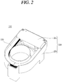
- FIG. 2 is a perspective view showing the current sensor unit 110 according to a preferred embodiment of the present disclosure
- FIG. 3 is a disassembled perspective view showing, in a disassembled manner, the current sensor unit 110 according to a preferred embodiment of the present disclosure
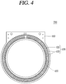
- FIG. 4 is a planar view showing a core and printed circuit board (PCB) coil assembly 230 among the current sensor unit 110 according to a preferred embodiment of the present disclosure
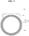
- FIG. 5 is a rear view showing the core and PCB coil assembly 230 according to a preferred embodiment of the present disclosure.
- PCB printed circuit board
- the current sensor unit 110 may include a power source unit 220, a core and PCB coil assembly 230, an insulating member 240, and an enclosure 250.
- the circuit 10 may pass through the current sensor unit 110 in one direction.
- the power source unit 220, the core and PCB coil assembly 230, and the insulating member 240 may be stacked on each other by being arranged in parallel in one direction.
- the power source unit 220 may be configured as a power current transformer (power CT), and may include an iron core and a secondary winding wound on the corresponding iron core.
- power CT power current transformer
- the iron core of the power source unit 220 may allow the circuit 10 to pass therethrough. Accordingly, the power source unit 220 may be arranged to enclose the circuit 10. This may allow a magnetic field generated from the circuit 10 to be applied to the power source unit 220.
- the power source unit 220 may generate a source current based on a current induced by the magnetic field, according to preset parameters. And the power source unit 220 may supply the source current to the controller 160.
- the controller 160 may operate by consuming the source current supplied from the power source unit 220.
- the core and PCB coil assembly 230 may pass the circuit 10 therethrough in one direction. And the core and PCB coil assembly 230 may enclose the circuit 10. Accordingly, a magnetic field generated by a current flowing on the circuit 10 may be applied to the core and PCB coil assembly 230. Here, the core and PCB coil assembly 230 may generate a secondary current induced by the magnetic field, in proportion to the amount of the current flowing on the circuit 10. And the core and PCB coil assembly 230 may transmit a secondary current to the controller 160. This may allow the controller 160 to calculate a primary current (i.e., a primary current amount) indicating the amount of the current flowing on the circuit 10, based on a secondary current.
- a primary current i.e., a primary current amount
- the core and PCB coil assembly 230 may be configured as an assembly of a core and a PCB of coil.
- the core and PCB coil assembly 230 may be formed as a circular or polygonal ring.
- the core and PCB coil assembly 230 may include a substrate part 410, a coil part 420 and a core part 430, as shown in FIGS. 4 and 5 .
- the substrate part 410 may support the coil part 420 and the core part 430.
- the substrate part 410 may be formed of a material having an electric insulating property.
- the substrate part 410 may be formed to have a flat structure.
- the substrate part 410 may be formed to have a single layer, or may be formed to have multi layers.
- the substrate part 410 may be provided with a through hole portion at a middle part thereof, in order to pass the circuit 10 therethrough in one direction.
- the surface of the substrate part 410 may be defined as a plane perpendicular to the one direction.
- the substrate part 410 may include a shielding part (not shown).
- the shielding part may be provided at the substrate part 410, in order to shield the core and PCB coil assembly 230, from external noise.
- the shielding part may be applied to a side surface of the substrate part 410, or may be connected to a ground.
- the shielding part may be formed of a coating layer of copper and/or lead.
- the coil part 420 may generate the secondary current from the applied magnetic field.
- the coil part 420 may include a plurality of conductive pads formed as straight lines of a predetermined length, at an upper surface and a bottom surface of the substrate part 410.
- the coil part 420 may enclose the circuit 10.
- the coil part 420 may be formed on the surface of the substrate part 410, and may be formed to pass through the substrate part 410.
- the coil part 420 may include a plurality of conductive pad portions 422 and a plurality of connection portions 423 (via hole portions).
- the conductive pad portions 422 may be formed on the upper surface and/or the bottom surface of the substrate part 410.
- the plurality of connection portions 423 may connect one pair of conductive pad portions 422 corresponding to each other on the upper surface and the bottom surface of the substrate part 410, mechanically and electrically.
- the core part 430 may provide a magnetic path where a magnetic field formed around the circuit 10 is moveable.
- the core part 430 may be mounted to the substrate part 410.
- the core part 430 may enclose the circuit 10.
- the core part 430 may be arranged to be spaced apart from the coil part 420. That is, the core part 430 may not contact the coil part 420.
- the core part 430 may be configured as an iron core having a small thickness of 0.1-0.5 mm and having a higher magnetic permeability than air, according to a preferred embodiment.
- the core part 430 is configured as an iron core having a high magnetic permeability, a larger voltage (e.g., several millivolts or more) than a very small induced voltage corresponding to several micro bolts when the core part is configured as an air core is induced to the coil part 420. Accordingly, an amplifying circuit for amplifying a small detection signal is not required.
- the core part 430 may be formed as a circular or polygonal ring.
- the coil part 420 may be wound on the core part 430. That is, the core part 430 may be arranged at an inner region of the conductive pad portions 422, between the conductive pad portions 422 formed on a front surface and a rear surface of the substrate part 410. For instance, in a case that the plurality of connection portions 423 connect both ends of the conductive pad portions 422 formed on an upper surface and a bottom surface of the substrate part 410, the core part 430 may be arranged between the plural pairs of connection portions 423.
- the insulating member 240 may be arranged between the power source unit 220 and the core and PCB coil assembly 230. This may allow the insulating member 240 to electrically separate the power source unit 220 and the core and PCB coil assembly 230 from each other.
- the insulating member 240 may be formed of an insulating material. And the insulating member 240 may allow the circuit 10 to pass therethrough in the one direction. Also, the insulating member 240 may enclose the circuit 10.
- the enclosure 250 may accommodate therein the power source unit 220, the core and PCB coil assembly 230, and the insulating member 240. And the enclosure 250 may support the power source unit 220, the core and PCB coil assembly 230, and the insulating member 240. Also, the enclosure 250 may allow the circuit 10 to pass therethrough in the one direction.
- the enclosure 250 may include a first enclosure 251 and a second enclosure 253.
- the first enclosure 251 may be arranged to face the power source 20, and the second enclosure 253 may be arranged to face the load 30.
- the first enclosure 251 and the second enclosure 253 may be coupled to each other in one direction.
- the first enclosure 251 and the second enclosure 253 may be coupled to each other, at an outer region of the power source unit 220, the core and PCB coil assembly 230, and the insulating member 240.
- a primary current may flow to the load 30 from the power source 20 along the circuit 10. Accordingly, a magnetic field may be generated around the circuit 10 based on the primary current.
- the magnetic field may be applied to the power source unit 220 and the core and PCB coil assembly 230, of the current sensor unit 110.
- the magnetic field may be applied to the coil part 420 of the core and PCB coil assembly 230.
- the power source unit 220 may generate a source current from a magnetic field, thereby supplying to the controller 160.
- the core and PCB coil assembly 230 may generate a secondary current from a magnetic field, thereby outputting a voltage corresponding to the secondary current to the controller 160.
- the core part 430 may provide a magnetic movement path of a magnetic field applied to the coil part 420. This may allow the controller 160 to operate by the source current, and to calculate the amount of the primary current based on a voltage.
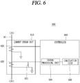
- FIG. 6 is a block diagram showing an electric configuration of a current sensing device according to a first embodiment of the present disclosure.
- a current sensing device 600 may include a current sensor unit 610 and a controller 660.
- a circuit 10 connects a power source 20 and a load 30, and a current may flow from the power source 20 to the load 30 along the circuit 10.
- a primary current may be defined as the current flowing on the circuit 10.
- the current sensor unit 610 may include a power source unit 620, and a core and PCB coil assembly 630.
- the power source unit 620 and the core and PCB coil assembly 630 may be arranged in parallel to each other in one direction. And the power source unit 620 and the core and PCB coil assembly 630 may pass the circuit 10 therethrough in one direction. Also, the power source unit 620 and the core and PCB coil assembly 630 may enclose the circuit 10. This may allow a magnetic field generated at the circuit 10 to be applied to the power source unit 620 and the core and PCB coil assembly 630.
- the power source unit 620 may generate a source current from a magnetic field, thereby supplying to the controller 660.
- the core and PCB coil assembly 630 may generate a secondary current from a magnetic field.
- the core and PCB coil assembly 630 may include a load (burden) 635 for providing a current detection signal as a voltage signal.
- the load 635 may provide a voltage formed at both ends of the load 635 to the controller, as an input signal for current measurement, in correspondence to the secondary current.
- the load 635 may be configured as a resistance having a preset resistance value, or a capacitor.
- the controller 660 may operate by using a source current of the power source unit 620. And the controller 660 may calculate the amount of a primary current flowing on the circuit 10, based on the secondary current. According to the first embodiment, the controller 660 may include a signal processing unit 680 and a calculation unit 690.
- the signal processing unit 680 may convert an analogue detection signal of a secondary current outputted from the current sensor unit 610, into a digital signal.
- the calculation unit 690 may calculate the amount of the primary current flowing on the circuit 10, based on the digital signal of the secondary current. That is, the calculation unit 690 may calculate the primary current based on a digital voltage signal corresponding to the secondary current.
- the controller 660 pre-stores therein parameters of the current sensor unit 610, and the calculation unit 690 may calculate a primary current by using them.
- the controller 660 stores therein a voltage indicated by the digital voltage signal, and the amount of the primary current, in a mapping manner. As the calculation unit 690 selects a primary current in correspondence to the voltage, the amount (value) of the primary current may be output.
- FIG. 7 is a partially-cut perspective view showing an inner configuration of the core and PCB coil assembly shown in FIG. 4 in a partially-cut manner.
- FIG. 8 is a sectional view showing an inner configuration of the core and PCB coil assembly 630 according to a first embodiment of the present disclosure.
- FIG. 8 is a sectional view taken along line A-A' in FIG. 7 .
- the core and PCB coil assembly 630 may include a substrate part 710, a coil part 720 and a core part 730.
- FIG. 7 shows a state that the substrate part 710 and the coil part 720 have been removed from a partial region of the core and PCB coil assembly 630.
- the core and PCB coil assembly 630 may be implemented as a PCB.
- the substrate part 710 may support the coil part 720 and the core part 730.
- the substrate part 710 may be formed of an electric insulating material.
- the substrate part 710 may include a plurality of base substrates 711, 713.
- the base substrates 711, 713 may be stacked on each other in one direction.
- each of the base substrates 711, 713 may be formed to have a flat structure.
- each of the base substrates 711, 713 may be formed to have a single layer, or may be formed to have multi layers.
- the base substrates 711, 713 may include the first base substrate 711, and the second base substrates 713 mounted to both side surfaces (an upper surface and a bottom surface in FIG. 7 ) of the first base substrate 711.
- the coil part 720 may generate a secondary current from an applied magnetic field.
- the coil part 720 may be mounted to the substrate part 710.
- the coil part 720 may be formed of a conductive material such as copper.
- the coil part 720 may include conductive pad portions 722 and connection portions 723.
- the conductive pad portions 722 may be mounted (printed) to (on) the surface of the substrate part 710.
- the conductive pad portions 722 may be mounted to the second base substrates 713, on the opposite side to the first base substrate 711.
- the connection portions 723 may pass through the substrate part 710. And the connection portions 723 may connect the conductive pad portion 722 corresponding to the upper base substrate 713, to the conductive pad portion corresponding to the lower base substrate 713, in FIG. 8 .
- connection portions 723 may pass through the first base substrate 711 and the second base substrates 713.
- any two of the connection portions 723 may be connected to both ends of one of the conductive pad portions 722 on one surface of the substrate part 710, and may be connected to both ends of another of the conductive pad portions 722 on another surface of the substrate part 710, respectively.
- the core part 730 may be configured as an iron core to thus enhance a magnetic field applied to the coil part 720. This may allow the core part 730 to generate a larger induced voltage than that when the core part 730 is configured as an air core, at the coil part 720. Accordingly, an amplifying circuit for amplifying an induced voltage is not required.
- the core part 730 may be mounted to the substrate part 710. And the core part 730 may be implemented to have a ring shape.
- the core part 730 may be inserted into an inner region of the substrate part 710. As FIG. 7 can be referred to, the core part 730 may pass through the first base substrate 711. Though this, the core part 730 may be separated from the conductive pad portions 722 by a boundary of the second base substrates 713, and may be separated from the connection portions 723 by a boundary of the first base substrate 711 and the second base substrates 713.
- FIG. 9 is a block diagram showing an electric configuration of a current sensing device according to a second embodiment of the present disclosure.
- a current sensing device 900 may include a current sensor unit 910 and a controller 960.
- a circuit 10 connects a power source 20 and a load 30, and a current may flow from the power source 20 to the load 30 along the circuit 10.
- a primary current may be defined as the current flowing on the circuit 10.
- a first magnetic field may be defined as a magnetic field generated at the circuit 10, based on the primary current.
- the current sensor unit 910 may include a power source unit 920, and a core and PCB coil assembly 930.
- the power source unit 920 and the core and PCB coil assembly 930 may be stacked on each other by being arranged in parallel to each other in one direction. And the power source unit 920 and the core and PCB coil assembly 930 may pass the circuit 10 therethrough in the one direction. Also, the power source unit 920 and the core and PCB coil assembly 930 may enclose the circuit 10. This may allow a first magnetic field to be applied to the power source unit 920 and the core and PCB coil assembly 930.
- the power source unit 920 may generate a source current from a first magnetic field, thereby supplying to the controller 960.
- the core and PCB coil assembly 930 may generate a secondary current by a voltage induced from a first magnetic field.
- the core and PCB coil assembly 930 may include a first core and PCB coil assembly 931 (hereinafter, will be abbreviated as a first assembly), and a second core and PCB coil assembly 933 (hereinafter, will be abbreviated as a second assembly).
- the first assembly 931 may generate a second magnetic field, based on a source current applied from the controller 960. This may allow a part of a first magnetic field to be attenuated by a second magnetic field.
- the second assembly 933 may generate a secondary current, based on a current induced by the rest of a first magnetic field and a compensation current applied from the controller 960.
- the second assembly 933 may include a load 935.
- the load 935 may provide a voltage formed at both ends of the load 935 to the controller 960, as an input signal for current measurement, in correspondence to the secondary current.
- the load 935 may be configured as a resistance having a preset resistance value, or a capacitor.
- the controller 960 may operate by using a source current of the power source unit 920. And the controller 960 may calculate the amount of a primary current flowing on the circuit 10, based on the secondary current. According to the second embodiment, the controller 960 may include a compensation unit 970, a signal processing unit 980 and a calculation unit 990.
- the compensation unit 970 may apply a compensation current to the current sensor unit 910.
- the compensation unit 970 may include an oscillation unit 971, a comparison unit 973, and a feedback controller 975.
- the oscillation unit 971 may apply a source current to the first assembly 931.
- the oscillation unit 971 may generate a chopping wave or a square wave as the source power having a phase difference of 180° from the primary current flowing on the circuit 10, and may apply it to the first assembly 931.
- the reason is in order to generate a magnetic field having an opposite direction to a magnetic field formed by the primary current, by the source current, for partial attenuation.
- the second magnetic field generated from the first assembly 931 may attenuate the first magnetic field generated by the primary current flowing on the circuit 10, at least partially, by the source current outputted from the oscillation unit 971. Such a partial attenuation may reduce an output voltage of the current sensor unit 910, corresponding to the amount of the primary current flowing on the circuit 10, and thus it is required to compensate for that.
- the comparison unit 973 may determine a compensation current to compensate for a part of a first magnetic field.
- the comparison unit 973 may compare a present output voltage outputted from the current sensor unit 910 to a previous output voltage, thereby determining a corresponding compensation current.
- the comparison unit 973 may compare a present output voltage outputted from the current sensor unit 910 to a previous output voltage, thereby requesting the feedback controller 975 to output a compensation current corresponding to a difference value between the present output voltage and the previous output voltage.
- the feedback controller 975 may apply the corresponding compensation current to the second assembly 933, in response to the request of the comparison unit 973.
- the signal processing unit 980 may convert an analogue voltage signal as the output voltage provided from the current sensor unit 910, into a digital signal.
- the signal processing unit 980 may output the voltage signal converted into the digital signal, to the calculation unit 990.
- the calculation unit 990 may calculate the amount of a primary current flowing on the circuit 10, based on the digital signal, the voltage signal.
- the controller 960 pre-stores therein parameters of the current sensor unit 910, and the calculation unit 990 may output the amount (value) of the primary current by using them. That is, the controller 960 stores therein a voltage value of the digital signal, and the amount of the primary current, in a mapping manner. As the calculation unit 990 selects the primary current corresponding to the voltage value, the calculation may be performed.
- FIG. 10 is a sectional view showing an inner configuration of a core and PCB coil assembly 930 according to a second embodiment.
- the core and PCB coil assembly 930 may include a substrate part 1010, a coil part 1020 and a core part 1030.
- the substrate part 1010 may support the coil part 1020 and the core part 1030.
- the substrate part 1010 may include a plurality of base substrates 1011, 1013, 1015.
- the base substrates 1011, 1013, 1015 may be stacked on each other in one direction.
- each of the base substrates 1011, 1013, 1015 may be formed to have a flat structure.
- each of the base substrates 1011, 1013, 1015 may be formed to have a single layer, or may be formed to have multi layers.
- the base substrates 1011, 1013, 1015 may include the first base substrate 1011, the second base substrates 1013 mounted to both side surfaces (an upper surface and a bottom surface in FIG. 10 ) of the first base substrate 1011, and the third base substrates 1015 mounted to the second base substrates 1013, respectively.
- the coil part 1020 may generate a secondary current from an applied magnetic field.
- the coil part 1020 may be mounted to the substrate part 1010.
- the coil part 1020 may be formed of a conductive material such as copper.
- the coil part 1020 may include a first coil part 1021 and a second coil part 1025.
- the first coil part 1021 may serve as the coil part (secondary winding) among the first assembly 931 of FIG. 9
- the second coil part 1025 may serve as the coil part (secondary winding) among the second assembly 933 of FIG. 9 .
- the first coil part 1021 may include first conductive pad portions 1022 and first connection portions 1023 (first via hole portions).
- the first conductive pad portions 1022 may be mounted (printed) to (on) the surface of the second base substrate 1013.
- the first conductive pad portions 1022 may be arranged between the second base substrates 1013 and the third base substrates 1015.
- the first connection portions 1023 may pass through the first base substrate 1011 and the second base substrates 1013.
- the first connection portions 1023 may connect the first conductive pad portions 1022 to each other. For instance, any two of the first connection portions 1023 may be connected to both ends of one of the first conductive pad portions 1022 on one surface (an upper surface in FIG.
- the second base substrate 1013 (especially, the upper one of the two second base substrates), and may be connected to both ends of another of the first conductive pad portions 1022 on another surface (a bottom surface in FIG. 10 ) of the second base substrate 1013 (especially, the lower one of the two second base substrates), respectively.
- the second coil part 1025 may include second conductive pad portions 1026 (refer to 722 of FIG. 7 for a detailed configuration), and second connection portions 1027 (refer to 723 of FIG. 7 for a detailed configuration).
- the second conductive pad portions 1026 may be mounted (printed) to (on) the surface of the third base substrate 1015.
- the second connection portions 1027 may pass through the first base substrate 1011, the second base substrates 1013, and the third base substrates 1015.
- the second connection portions 1027 may connect the second conductive pad portions 1026 to each other. For instance, any two of the second connection portions 1027 may be connected to both ends of one of the second conductive pad portions 1026 on one surface (an upper surface in FIG.
- the third base substrate 1015 (the upper one of the two third base substrates in FIG. 10 ), and may be connected to both ends of another of the second conductive pad portions 1026 on another surface (a bottom surface in FIG. 10 ) of the third base substrate 1015 (the lower one of the two third base substrates in FIG. 10 ), respectively.
- the core part 1030 may be configured as an iron core to thus enhance a magnetic field applied to the coil part 1020. This may allow the core part 1030 to generate a comparatively larger induced voltage requiring no signal amplification, than that when the core part 1030 is configured as an air core, at the coil part 1020.
- the core part 1030 may be mounted to the substrate part 1010. And the core part 1030 may be implemented to have a ring shape.
- the core part 1030 may be inserted into an inner region of the substrate part 1010.
- the core part 1030 may pass through the first base substrate 1011.
- FIG. 11 is a sectional view showing a core and PCB coil assembly 930 according to a third embodiment of the present disclosure.
- the core and PCB coil assembly 930 may include a first core and PCB coil assembly 931 (hereinafter, will be abbreviated as a first assembly), and a second core and PCB coil assembly 933 (hereinafter, will be abbreviated as a second assembly).
- first assembly 931 and the second assembly 933 may be implemented as a PCB.
- the first assembly 931 may include a first substrate part 1110, a first coil part 1120, and a first core part 1130.
- the first substrate part 1110 may include base substrates 1111, 1113, and the first coil part 1120 may include first conductive pad portions 1122 and first connection portions 1123.
- the second assembly 933 may include a second substrate part 1150, a second coil part 1160, and a second core part 1170.
- the second substrate part 1150 may include base substrates 1151, 1153, and the second coil part 1160 may include second conductive pad portions 1162 and second connection portions 1163.
- the first assembly 931 and the second assembly 933 of the core and PCB coil assembly 930 according to the third embodiment are similar to the core and PCB coil assembly 630 according to the first embodiment, respectively. And thus detailed explanations thereof will be omitted.
- a separation part 1180 may be arranged between the first core and PCB coil assembly 931 and the second core and PCB coil assembly 933. And the separation part 1180 may separate the first assembly 931 and the second assembly 933 from each other.
- the separation part 1180 may be formed of a material having an electric insulating property.
- the core and PCB coil assembly 930 may further include another core part (not shown) and other separation parts (not shown). Another core part may be arranged between the first substrate part 1110 and the second substrate part 1150.
- the first assembly 931 may not include the first core part 1130
- the second assembly 933 may not include the second core part 1170.
- Other separation parts may be arranged between the first assembly 931 and another core part, and between another core part and the second assembly 933. Other separation parts may prevent a contact between the first assembly 931 and another core part, and a contact between another core part and the second assembly 933.
- a primary current may flow to the load 30 from the power source 20 along the circuit 10.
- a first magnetic field may be generated around the circuit 10 based on the primary current.
- the magnetic field may be applied to the power source unit 920 and the core and PCB coil assembly 930, of the current sensor unit 910.
- the power source unit 920 may supply a source current induced from the first magnetic field, to the controller 960.
- the controller 960 may apply the source current to the first assembly 931.
- the first assembly 931 may generate a second magnetic field, based on the source current. This may allow a part of the first magnetic field to be attenuated by the second magnetic field. And the rest of the first magnetic field may be applied to the second assembly 933.
- the controller 960 may apply a compensation current to compensate for a part of the first magnetic field, to the second assembly 933. This may allow the second assembly 933 to generate a secondary current, based on a current induced by the rest of the first magnetic field and the compensation current. Here, the second assembly 933 may output a voltage corresponding to the secondary current, to the controller 960. This may allow the controller 960 to calculate a primary current based on the voltage.
- the core and PCB coil assembly 930 may further include a third core and PCB coil assembly (not shown), and another separation part (not shown).
- the third core and PCB coil assembly (not shown) may sense one current among an anode and a cathode of a direct current circuit, and the first assembly 931 and the second assembly 933 may sense another current among the anode and the cathode of the direct current circuit. This may allow the current sensor unit 910 of the current sensing device to detect the amount of a current on a direct current circuit.
- the assembly of the third core and the PCB of coil may include an oscillation circuit.
- the assembly of the third core and the PCB of coil may be implemented as a PCB.
- the assembly of the third core and the PCB of coil may be implemented similarly to the core and PCB coil assembly 630 according to the first embodiment. And the assembly of the third core and the PCB of coil may be stacked on at least one of the first assembly 931 and the second assembly 933. Another separation part may be arranged between at least one of the first assembly 931 and the second assembly 933 and the assembly of the third core and the PCB of coil. And another separation part may separate at least one of the first assembly 931 and the second assembly 933 and the assembly of the third core and the PCB of coil from each other.
- another separation part may be formed of a material having an electric insulating property.
- the core and PCB coil assemblies 230, 630, 930 are fabricated with a structure that the coil parts 420, 720, 1020, 1120, 1160 are printed on the substrate parts 410, 710, 1010, 1110, 1150.
- the core and PCB coil assemblies 230, 630, 930 may be automatically fabricated by a manufacturing machine, and the current sensor unit may have uniform characteristics.
- the core and PCB coil assemblies 230, 630, 930 include the core parts 430, 730, 1030, 1130, 1170 which are configured as iron cores of a high magnetic permeability.
- the core parts 430, 730, 1030, 1130, 1170 may enhance a magnetic field applied to the core and PCB coil assemblies 230, 630, 930, from the circuit 10. And a larger induced voltage than that when the core parts are configured as air cores may be obtained. Accordingly, an amplifying circuit for amplifying a current detection signal (a voltage signal finally outputted from the current sensor unit) is not required. And it is easy to separate a current detection signal even if external noise is mixed with the signal. Further, the current sensing devices 100, 600, 900 attenuate a part of a magnetic field generated at the circuit 10, and compensate it by a compensation current, thereby preventing a magnetic saturation.
Landscapes
- Engineering & Computer Science (AREA)
- Power Engineering (AREA)
- Physics & Mathematics (AREA)
- General Physics & Mathematics (AREA)
- Microelectronics & Electronic Packaging (AREA)
- Measuring Instrument Details And Bridges, And Automatic Balancing Devices (AREA)
- Measurement Of Current Or Voltage (AREA)
Abstract
Description
- The present disclosure relates to a current sensing device.
- Generally, a circuit breaker opens and closes a circuit. Here, the circuit breaker is installed on a circuit between a power source and a load. And the circuit breaker connects a circuit, or interrupts a circuit. Here, the circuit breaker analyzes a current flowing on a circuit. Through this, if a current on a circuit is a normal current, the circuit breaker connects the circuit. On the other hand, if a current on a circuit is an abnormal current, the circuit breaker interrupts the circuit.
- For this, the circuit breaker includes a current sensing device for sensing a current on a circuit.
- As such a current sensing device, a current transformer is generally used much. However, in case of a high-capacity circuit breaker having a large load current, a current transformer includes an iron core. This causes problems of a magnetic saturation with respect to a large current and a heat occurrence due to an iron loss. Accordingly, in a circuit breaker of a large capacity, a Rogowskii coil comparatively having no magnetic saturation is used.
- The conventional current sensing device using such a Rogowskii coil includes an air core formed of an insulating material such as plastic and formed to enclose a circuit, and a coil wound on the air core and on which a current induced by a magnetic field of the circuit flows. The current sensing device may calculate the amount of a current flowing on a circuit, on the basis of a voltage signal induced by a magnetic field generated around the circuit, based on an electromagnetic induction.
- However, there is a problem that a performance of the conventional current sensing device is not uniformly obtained. That is, the current sensing device may have a different performance according to its fabrication environment. The reason is because fabrication processes such as winding a coil on an air core are performed manually. As a result, a current calculated from the current sensing device has a low reliability, and a circuit breaker may malfunction.
- Further, in the conventional current sensing device, since an air core is used, an output signal corresponds to several micro bolts (µV) when a rated voltage is low. This may cause a problem that an amplifying circuit should be additionally installed. Also, it was difficult to select an output signal when external noise was mixed with the signal.
- An object of the present disclosure is to provide a current sensing device capable of minimizing manual procedures at the time of fabrication processes.
- Another object of the present disclosure is to provide a current sensing device capable of uniformly obtaining a product performance.
- Another object of the present disclosure is to provide a current sensing device capable of enhancing the reliability on a found current detection signal.
- Another object of the present disclosure is to provide a current sensing device capable of preventing a malfunction of a circuit breaker where the current sensing device of the present disclosure has been installed.
- A current sensing device according to the present disclosure, which achieves the purposes of the present disclosure, may include: a substrate part which includes at least two base substrates stacked in one direction and through which a circuit passes in the one direction; a coil part which is formed on at least one of the base substrates, and which surrounds the circuit; and a core part which is disposed between the base substrates while being spaced apart from the coil part, and which surrounds the circuit.
- According to one preferred aspect of the present disclosure, the coil part may include: a first coil part configured to attenuate a part of a magnetic field generated at the circuit; and a second coil part configured to generate a current induced from the rest of the magnetic field.
- According to another preferred aspect of the present disclosure, the current sensing device may further include a compensation unit configured to apply a compensation current for compensating for a part of the magnetic field, to the second coil part.
- According to still another preferred aspect of the present disclosure, the second coil part may be further configured to output a voltage corresponding to the induced current and the compensation current.
- According to one preferred aspect of the present disclosure, the current sensing device may further include: an oscillation unit configured to apply a source current for driving the first coil part; and a calculation unit configured to calculate a current flowing on the circuit, based on the voltage.
- According to a preferred aspect of the present disclosure, since a core and printed circuit board (PCB) coil assembly is fabricated with a structure that the coil part is formed on the substrate part, the core and PCB coil assembly may be easily fabricated.
- As the core and PCB coil assembly includes the core part, the core part may enhance a magnetic field applied to the core and PCB coil assembly, from the circuit.
- Further, the current sensing device attenuates a part of a magnetic field generated at the circuit, and compensates it by a compensation current, thereby preventing a magnetic saturation due to a magnetic field. This may allow manual procedures to be minimized while the current sensing device is fabricated, and the current sensing device may have a uniform performance.
- Accordingly, the reliability on a current detection signal (current detection data) detected by the current sensing device may be enhanced. Further, a malfunction of a circuit breaker due to a current detection signal may be prevented.
-
-
FIG. 1 is a block diagram showing an electric configuration of a current sensing device according to the present disclosure. -
FIG. 2 is a perspective view showing an assembled state of a physical configuration of a current sensor unit in a current sensing device according to the present disclosure. -
FIG. 3 is a disassembled perspective view showing a disassembled state of an assembly of the current sensor unit shown inFIG. 2 . -
FIG. 4 is a planar view showing a core and printed circuit board (PCB) coil assembly among a current sensor unit, a major component of a current sensing device according to the present disclosure. -
FIG. 5 is a rear view showing a rear surface of the core and PCB coil assembly shown inFIG. 4 . -
FIG. 6 is a block diagram showing an electric configuration of a current sensing device according to a first embodiment of the present disclosure. -
FIG. 7 is a partially-cut perspective view showing an inner configuration of the core and PCB coil assembly shown inFIG. 4 in a partially-cut manner. -
FIG. 8 is a sectional view taken along line A-A' inFIG. 7 , which shows an inner configuration of a core and PCB coil assembly according to a first embodiment of the present disclosure. -
FIG. 9 is a block diagram showing an electric configuration of a current sensing device according to a second embodiment of the present disclosure. -
FIG. 10 is a sectional view showing, in a partially-cut manner, an inner configuration of a core and PCB coil assembly among the current sensing device according to a second embodiment of the present disclosure. -
FIG. 11 is a sectional view showing, in a partially-cut manner, an inner configuration of a core and PCB coil assembly among a current sensing device according to a third embodiment of the present disclosure. - Hereinafter, various embodiments of the present disclosure will be explained with reference to the accompanying drawings. However, this is not to limit the technique disclosed in this specification to a specific embodiment, but it should be understood that various modifications, equivalents, and/or alternatives are included. In relation to explanations of the drawings, similar components may be provided with similar reference numbers.
- Terms such as "have", "may have", "include" or "may include" are used to indicate an existence of a corresponding characteristic (e.g., numbers, functions, operations, or components such as parts), and they do not exclude an existence of an additional characteristic.
- The terms such as "first" or "second" may modify various elements regardless of the order and/or the importance, and are merely used to distinguish one element from another. They do not limit corresponding elements.
-
FIG. 1 is a block diagram showing an electric configuration of acurrent sensing device 100 according to a first embodiment of the present disclosure. - Referring to
FIG. 1 , thecurrent sensing device 100 according to a first embodiment of the present disclosure may be arranged on acircuit 10. Here, thecircuit 10 may be an electric power circuit of an electric power system (grid). Thecircuit 10 connects apower source 20 and aload 30 to each other, and a current may flow from thepower source 20 to theload 30 along thecircuit 10. Here, a primary current may be defined as the current flowing on thecircuit 10. Thecurrent sensing device 100 may include acurrent sensor unit 110 and acontroller 160. - The
current sensor unit 110 may detect a secondary current based on a primary current. Here, as the primary current flows on thecircuit 10, a magnetic field may be generated around thecircuit 10. This may allow a magnetic field to be applied to thecurrent sensor unit 110. And thecurrent sensor unit 110 may detect a secondary current in correspondence to a magnetic field. Thecurrent sensor unit 110 may generate a secondary current from a magnetic field by an electromagnetic induction. That is, a secondary current may be defined as a current induced from a magnetic field. - The
controller 160 may calculate a primary current based on a secondary current. Here, thecontroller 160 may detect a voltage based on a secondary current. And thecontroller 160 may calculate a primary current from a voltage. Here, thecontroller 160 may pre-store parameters of thecurrent sensor unit 110, and may calculate a primary current by using them. -
FIG. 2 is a perspective view showing thecurrent sensor unit 110 according to a preferred embodiment of the present disclosure, andFIG. 3 is a disassembled perspective view showing, in a disassembled manner, thecurrent sensor unit 110 according to a preferred embodiment of the present disclosure.FIG. 4 is a planar view showing a core and printed circuit board (PCB)coil assembly 230 among thecurrent sensor unit 110 according to a preferred embodiment of the present disclosure. AndFIG. 5 is a rear view showing the core andPCB coil assembly 230 according to a preferred embodiment of the present disclosure. - Referring to
FIGS. 2 and3 , thecurrent sensor unit 110 according to a preferred embodiment of the present disclosure may include apower source unit 220, a core andPCB coil assembly 230, an insulatingmember 240, and anenclosure 250. Thecircuit 10 may pass through thecurrent sensor unit 110 in one direction. Here, thepower source unit 220, the core andPCB coil assembly 230, and the insulatingmember 240 may be stacked on each other by being arranged in parallel in one direction. - The
power source unit 220 may be configured as a power current transformer (power CT), and may include an iron core and a secondary winding wound on the corresponding iron core. - The iron core of the
power source unit 220 may allow thecircuit 10 to pass therethrough. Accordingly, thepower source unit 220 may be arranged to enclose thecircuit 10. This may allow a magnetic field generated from thecircuit 10 to be applied to thepower source unit 220. Here, thepower source unit 220 may generate a source current based on a current induced by the magnetic field, according to preset parameters. And thepower source unit 220 may supply the source current to thecontroller 160. Thus, thecontroller 160 may operate by consuming the source current supplied from thepower source unit 220. - The core and
PCB coil assembly 230 may pass thecircuit 10 therethrough in one direction. And the core andPCB coil assembly 230 may enclose thecircuit 10. Accordingly, a magnetic field generated by a current flowing on thecircuit 10 may be applied to the core andPCB coil assembly 230. Here, the core andPCB coil assembly 230 may generate a secondary current induced by the magnetic field, in proportion to the amount of the current flowing on thecircuit 10. And the core andPCB coil assembly 230 may transmit a secondary current to thecontroller 160. This may allow thecontroller 160 to calculate a primary current (i.e., a primary current amount) indicating the amount of the current flowing on thecircuit 10, based on a secondary current. For instance, the core andPCB coil assembly 230 may be configured as an assembly of a core and a PCB of coil. Here, the core andPCB coil assembly 230 may be formed as a circular or polygonal ring. According to various embodiments, the core andPCB coil assembly 230 may include asubstrate part 410, acoil part 420 and acore part 430, as shown inFIGS. 4 and5 . - The
substrate part 410 may support thecoil part 420 and thecore part 430. Here, thesubstrate part 410 may be formed of a material having an electric insulating property. And thesubstrate part 410 may be formed to have a flat structure. For instance, thesubstrate part 410 may be formed to have a single layer, or may be formed to have multi layers. Thesubstrate part 410 may be provided with a through hole portion at a middle part thereof, in order to pass thecircuit 10 therethrough in one direction. Here, the surface of thesubstrate part 410 may be defined as a plane perpendicular to the one direction. Thesubstrate part 410 may include a shielding part (not shown). The shielding part may be provided at thesubstrate part 410, in order to shield the core andPCB coil assembly 230, from external noise. For this, the shielding part may be applied to a side surface of thesubstrate part 410, or may be connected to a ground. The shielding part may be formed of a coating layer of copper and/or lead. - The
coil part 420 may generate the secondary current from the applied magnetic field. For this, thecoil part 420 may include a plurality of conductive pads formed as straight lines of a predetermined length, at an upper surface and a bottom surface of thesubstrate part 410. Here, thecoil part 420 may enclose thecircuit 10. And thecoil part 420 may be formed on the surface of thesubstrate part 410, and may be formed to pass through thesubstrate part 410. Thecoil part 420 may include a plurality ofconductive pad portions 422 and a plurality of connection portions 423 (via hole portions). Theconductive pad portions 422 may be formed on the upper surface and/or the bottom surface of thesubstrate part 410. The plurality ofconnection portions 423 may connect one pair ofconductive pad portions 422 corresponding to each other on the upper surface and the bottom surface of thesubstrate part 410, mechanically and electrically. - The
core part 430 may provide a magnetic path where a magnetic field formed around thecircuit 10 is moveable. For this, thecore part 430 may be mounted to thesubstrate part 410. Here, thecore part 430 may enclose thecircuit 10. And thecore part 430 may be arranged to be spaced apart from thecoil part 420. That is, thecore part 430 may not contact thecoil part 420. Here, thecore part 430 may be configured as an iron core having a small thickness of 0.1-0.5 mm and having a higher magnetic permeability than air, according to a preferred embodiment. In the present disclosure, since thecore part 430 is configured as an iron core having a high magnetic permeability, a larger voltage (e.g., several millivolts or more) than a very small induced voltage corresponding to several micro bolts when the core part is configured as an air core is induced to thecoil part 420. Accordingly, an amplifying circuit for amplifying a small detection signal is not required. - Further, the
core part 430 may be formed as a circular or polygonal ring. Thecoil part 420 may be wound on thecore part 430. That is, thecore part 430 may be arranged at an inner region of theconductive pad portions 422, between theconductive pad portions 422 formed on a front surface and a rear surface of thesubstrate part 410. For instance, in a case that the plurality ofconnection portions 423 connect both ends of theconductive pad portions 422 formed on an upper surface and a bottom surface of thesubstrate part 410, thecore part 430 may be arranged between the plural pairs ofconnection portions 423. - The insulating
member 240 may be arranged between thepower source unit 220 and the core andPCB coil assembly 230. This may allow the insulatingmember 240 to electrically separate thepower source unit 220 and the core andPCB coil assembly 230 from each other. Here, the insulatingmember 240 may be formed of an insulating material. And the insulatingmember 240 may allow thecircuit 10 to pass therethrough in the one direction. Also, the insulatingmember 240 may enclose thecircuit 10. - The
enclosure 250 may accommodate therein thepower source unit 220, the core andPCB coil assembly 230, and the insulatingmember 240. And theenclosure 250 may support thepower source unit 220, the core andPCB coil assembly 230, and the insulatingmember 240. Also, theenclosure 250 may allow thecircuit 10 to pass therethrough in the one direction. Theenclosure 250 may include afirst enclosure 251 and asecond enclosure 253. Thefirst enclosure 251 may be arranged to face thepower source 20, and thesecond enclosure 253 may be arranged to face theload 30. And thefirst enclosure 251 and thesecond enclosure 253 may be coupled to each other in one direction. Thefirst enclosure 251 and thesecond enclosure 253 may be coupled to each other, at an outer region of thepower source unit 220, the core andPCB coil assembly 230, and the insulatingmember 240. - According to various embodiments, a primary current may flow to the
load 30 from thepower source 20 along thecircuit 10. Accordingly, a magnetic field may be generated around thecircuit 10 based on the primary current. Here, the magnetic field may be applied to thepower source unit 220 and the core andPCB coil assembly 230, of thecurrent sensor unit 110. Here, the magnetic field may be applied to thecoil part 420 of the core andPCB coil assembly 230. Thepower source unit 220 may generate a source current from a magnetic field, thereby supplying to thecontroller 160. The core andPCB coil assembly 230 may generate a secondary current from a magnetic field, thereby outputting a voltage corresponding to the secondary current to thecontroller 160. Here, thecore part 430 may provide a magnetic movement path of a magnetic field applied to thecoil part 420. This may allow thecontroller 160 to operate by the source current, and to calculate the amount of the primary current based on a voltage. -
FIG. 6 is a block diagram showing an electric configuration of a current sensing device according to a first embodiment of the present disclosure. - Referring to
FIG. 6 , acurrent sensing device 600 according to a first embodiment of the present disclosure may include acurrent sensor unit 610 and acontroller 660. Here, acircuit 10 connects apower source 20 and aload 30, and a current may flow from thepower source 20 to theload 30 along thecircuit 10. Here, a primary current may be defined as the current flowing on thecircuit 10. - The
current sensor unit 610 may include apower source unit 620, and a core andPCB coil assembly 630. Here, thepower source unit 620 and the core andPCB coil assembly 630 may be arranged in parallel to each other in one direction. And thepower source unit 620 and the core andPCB coil assembly 630 may pass thecircuit 10 therethrough in one direction. Also, thepower source unit 620 and the core andPCB coil assembly 630 may enclose thecircuit 10. This may allow a magnetic field generated at thecircuit 10 to be applied to thepower source unit 620 and the core andPCB coil assembly 630. Thepower source unit 620 may generate a source current from a magnetic field, thereby supplying to thecontroller 660. The core andPCB coil assembly 630 may generate a secondary current from a magnetic field. According to the first embodiment, the core andPCB coil assembly 630 may include a load (burden) 635 for providing a current detection signal as a voltage signal. The load 635 may provide a voltage formed at both ends of the load 635 to the controller, as an input signal for current measurement, in correspondence to the secondary current. Here, the load 635 may be configured as a resistance having a preset resistance value, or a capacitor. - The
controller 660 may operate by using a source current of thepower source unit 620. And thecontroller 660 may calculate the amount of a primary current flowing on thecircuit 10, based on the secondary current. According to the first embodiment, thecontroller 660 may include asignal processing unit 680 and acalculation unit 690. - The
signal processing unit 680 may convert an analogue detection signal of a secondary current outputted from thecurrent sensor unit 610, into a digital signal. - The
calculation unit 690 may calculate the amount of the primary current flowing on thecircuit 10, based on the digital signal of the secondary current. That is, thecalculation unit 690 may calculate the primary current based on a digital voltage signal corresponding to the secondary current. Here, thecontroller 660 pre-stores therein parameters of thecurrent sensor unit 610, and thecalculation unit 690 may calculate a primary current by using them. Thecontroller 660 stores therein a voltage indicated by the digital voltage signal, and the amount of the primary current, in a mapping manner. As thecalculation unit 690 selects a primary current in correspondence to the voltage, the amount (value) of the primary current may be output. -
FIG. 7 is a partially-cut perspective view showing an inner configuration of the core and PCB coil assembly shown inFIG. 4 in a partially-cut manner. AndFIG. 8 is a sectional view showing an inner configuration of the core andPCB coil assembly 630 according to a first embodiment of the present disclosure. Here,FIG. 8 is a sectional view taken along line A-A' inFIG. 7 . - Referring to
FIGS. 7 and 8 , the core andPCB coil assembly 630 according to a preferred embodiment of the present disclosure may include asubstrate part 710, acoil part 720 and acore part 730. Here,FIG. 7 shows a state that thesubstrate part 710 and thecoil part 720 have been removed from a partial region of the core andPCB coil assembly 630. For instance, the core andPCB coil assembly 630 may be implemented as a PCB. - The
substrate part 710 may support thecoil part 720 and thecore part 730. Here, thesubstrate part 710 may be formed of an electric insulating material. Thesubstrate part 710 may include a plurality ofbase substrates base substrates base substrates first base substrate 711, and thesecond base substrates 713 mounted to both side surfaces (an upper surface and a bottom surface inFIG. 7 ) of thefirst base substrate 711. - The
coil part 720 may generate a secondary current from an applied magnetic field. For this, thecoil part 720 may be mounted to thesubstrate part 710. Here, thecoil part 720 may be formed of a conductive material such as copper. Thecoil part 720 may includeconductive pad portions 722 andconnection portions 723. Theconductive pad portions 722 may be mounted (printed) to (on) the surface of thesubstrate part 710. Here, theconductive pad portions 722 may be mounted to thesecond base substrates 713, on the opposite side to thefirst base substrate 711. Theconnection portions 723 may pass through thesubstrate part 710. And theconnection portions 723 may connect theconductive pad portion 722 corresponding to theupper base substrate 713, to the conductive pad portion corresponding to thelower base substrate 713, inFIG. 8 . Here, theconnection portions 723 may pass through thefirst base substrate 711 and thesecond base substrates 713. For instance, any two of theconnection portions 723 may be connected to both ends of one of theconductive pad portions 722 on one surface of thesubstrate part 710, and may be connected to both ends of another of theconductive pad portions 722 on another surface of thesubstrate part 710, respectively. - According to a preferable aspect of the present disclosure, the
core part 730 may be configured as an iron core to thus enhance a magnetic field applied to thecoil part 720. This may allow thecore part 730 to generate a larger induced voltage than that when thecore part 730 is configured as an air core, at thecoil part 720. Accordingly, an amplifying circuit for amplifying an induced voltage is not required. For this, thecore part 730 may be mounted to thesubstrate part 710. And thecore part 730 may be implemented to have a ring shape. Here, thecore part 730 may be inserted into an inner region of thesubstrate part 710. AsFIG. 7 can be referred to, thecore part 730 may pass through thefirst base substrate 711. Though this, thecore part 730 may be separated from theconductive pad portions 722 by a boundary of thesecond base substrates 713, and may be separated from theconnection portions 723 by a boundary of thefirst base substrate 711 and thesecond base substrates 713. -
FIG. 9 is a block diagram showing an electric configuration of a current sensing device according to a second embodiment of the present disclosure. - Referring to
FIG. 9 , acurrent sensing device 900 according to a second embodiment of the present disclosure may include acurrent sensor unit 910 and acontroller 960. Here, acircuit 10 connects apower source 20 and aload 30, and a current may flow from thepower source 20 to theload 30 along thecircuit 10. Here, a primary current may be defined as the current flowing on thecircuit 10. And a first magnetic field may be defined as a magnetic field generated at thecircuit 10, based on the primary current. - The
current sensor unit 910 may include apower source unit 920, and a core andPCB coil assembly 930. Here, thepower source unit 920 and the core andPCB coil assembly 930 may be stacked on each other by being arranged in parallel to each other in one direction. And thepower source unit 920 and the core andPCB coil assembly 930 may pass thecircuit 10 therethrough in the one direction. Also, thepower source unit 920 and the core andPCB coil assembly 930 may enclose thecircuit 10. This may allow a first magnetic field to be applied to thepower source unit 920 and the core andPCB coil assembly 930. Thepower source unit 920 may generate a source current from a first magnetic field, thereby supplying to thecontroller 960. The core andPCB coil assembly 930 may generate a secondary current by a voltage induced from a first magnetic field. According to the second embodiment, the core andPCB coil assembly 930 may include a first core and PCB coil assembly 931 (hereinafter, will be abbreviated as a first assembly), and a second core and PCB coil assembly 933 (hereinafter, will be abbreviated as a second assembly). - The
first assembly 931 may generate a second magnetic field, based on a source current applied from thecontroller 960. This may allow a part of a first magnetic field to be attenuated by a second magnetic field. - The
second assembly 933 may generate a secondary current, based on a current induced by the rest of a first magnetic field and a compensation current applied from thecontroller 960. Thesecond assembly 933 may include aload 935. Theload 935 may provide a voltage formed at both ends of theload 935 to thecontroller 960, as an input signal for current measurement, in correspondence to the secondary current. Here, theload 935 may be configured as a resistance having a preset resistance value, or a capacitor. - The
controller 960 may operate by using a source current of thepower source unit 920. And thecontroller 960 may calculate the amount of a primary current flowing on thecircuit 10, based on the secondary current. According to the second embodiment, thecontroller 960 may include acompensation unit 970, asignal processing unit 980 and acalculation unit 990. - The
compensation unit 970 may apply a compensation current to thecurrent sensor unit 910. Thecompensation unit 970 may include anoscillation unit 971, acomparison unit 973, and afeedback controller 975. Theoscillation unit 971 may apply a source current to thefirst assembly 931. - Here, the
oscillation unit 971 may generate a chopping wave or a square wave as the source power having a phase difference of 180° from the primary current flowing on thecircuit 10, and may apply it to thefirst assembly 931. The reason is in order to generate a magnetic field having an opposite direction to a magnetic field formed by the primary current, by the source current, for partial attenuation. - The second magnetic field generated from the
first assembly 931 may attenuate the first magnetic field generated by the primary current flowing on thecircuit 10, at least partially, by the source current outputted from theoscillation unit 971. Such a partial attenuation may reduce an output voltage of thecurrent sensor unit 910, corresponding to the amount of the primary current flowing on thecircuit 10, and thus it is required to compensate for that. - The
comparison unit 973 may determine a compensation current to compensate for a part of a first magnetic field. Here, thecomparison unit 973 may compare a present output voltage outputted from thecurrent sensor unit 910 to a previous output voltage, thereby determining a corresponding compensation current. Here, thecomparison unit 973 may compare a present output voltage outputted from thecurrent sensor unit 910 to a previous output voltage, thereby requesting thefeedback controller 975 to output a compensation current corresponding to a difference value between the present output voltage and the previous output voltage. - The
feedback controller 975 may apply the corresponding compensation current to thesecond assembly 933, in response to the request of thecomparison unit 973. - The
signal processing unit 980 may convert an analogue voltage signal as the output voltage provided from thecurrent sensor unit 910, into a digital signal. Here, thesignal processing unit 980 may output the voltage signal converted into the digital signal, to thecalculation unit 990. - The
calculation unit 990 may calculate the amount of a primary current flowing on thecircuit 10, based on the digital signal, the voltage signal. Here, thecontroller 960 pre-stores therein parameters of thecurrent sensor unit 910, and thecalculation unit 990 may output the amount (value) of the primary current by using them. That is, thecontroller 960 stores therein a voltage value of the digital signal, and the amount of the primary current, in a mapping manner. As thecalculation unit 990 selects the primary current corresponding to the voltage value, the calculation may be performed. -
FIG. 10 is a sectional view showing an inner configuration of a core andPCB coil assembly 930 according to a second embodiment. - Referring to
FIG. 10 , the core andPCB coil assembly 930 according to the second embodiment may include asubstrate part 1010, acoil part 1020 and acore part 1030. - The
substrate part 1010 may support thecoil part 1020 and thecore part 1030. Here, thesubstrate part 1010 may include a plurality ofbase substrates base substrates base substrates base substrates base substrates first base substrate 1011, thesecond base substrates 1013 mounted to both side surfaces (an upper surface and a bottom surface inFIG. 10 ) of thefirst base substrate 1011, and thethird base substrates 1015 mounted to thesecond base substrates 1013, respectively. - The
coil part 1020 may generate a secondary current from an applied magnetic field. For this, thecoil part 1020 may be mounted to thesubstrate part 1010. Here, thecoil part 1020 may be formed of a conductive material such as copper. Thecoil part 1020 may include afirst coil part 1021 and asecond coil part 1025. Here, thefirst coil part 1021 may serve as the coil part (secondary winding) among thefirst assembly 931 ofFIG. 9 , and thesecond coil part 1025 may serve as the coil part (secondary winding) among thesecond assembly 933 ofFIG. 9 . - The
first coil part 1021 may include firstconductive pad portions 1022 and first connection portions 1023 (first via hole portions). The firstconductive pad portions 1022 may be mounted (printed) to (on) the surface of thesecond base substrate 1013. Here, the firstconductive pad portions 1022 may be arranged between thesecond base substrates 1013 and thethird base substrates 1015. Thefirst connection portions 1023 may pass through thefirst base substrate 1011 and thesecond base substrates 1013. And thefirst connection portions 1023 may connect the firstconductive pad portions 1022 to each other. For instance, any two of thefirst connection portions 1023 may be connected to both ends of one of the firstconductive pad portions 1022 on one surface (an upper surface inFIG. 10 ) of the second base substrate 1013 (especially, the upper one of the two second base substrates), and may be connected to both ends of another of the firstconductive pad portions 1022 on another surface (a bottom surface inFIG. 10 ) of the second base substrate 1013 (especially, the lower one of the two second base substrates), respectively. - The
second coil part 1025 may include second conductive pad portions 1026 (refer to 722 ofFIG. 7 for a detailed configuration), and second connection portions 1027 (refer to 723 ofFIG. 7 for a detailed configuration). The secondconductive pad portions 1026 may be mounted (printed) to (on) the surface of thethird base substrate 1015. Thesecond connection portions 1027 may pass through thefirst base substrate 1011, thesecond base substrates 1013, and thethird base substrates 1015. And thesecond connection portions 1027 may connect the secondconductive pad portions 1026 to each other. For instance, any two of thesecond connection portions 1027 may be connected to both ends of one of the secondconductive pad portions 1026 on one surface (an upper surface inFIG. 10 ) of the third base substrate 1015 (the upper one of the two third base substrates inFIG. 10 ), and may be connected to both ends of another of the secondconductive pad portions 1026 on another surface (a bottom surface inFIG. 10 ) of the third base substrate 1015 (the lower one of the two third base substrates inFIG. 10 ), respectively. - The
core part 1030 may be configured as an iron core to thus enhance a magnetic field applied to thecoil part 1020. This may allow thecore part 1030 to generate a comparatively larger induced voltage requiring no signal amplification, than that when thecore part 1030 is configured as an air core, at thecoil part 1020. For this, thecore part 1030 may be mounted to thesubstrate part 1010. And thecore part 1030 may be implemented to have a ring shape. Here, thecore part 1030 may be inserted into an inner region of thesubstrate part 1010. Thecore part 1030 may pass through thefirst base substrate 1011. -
FIG. 11 is a sectional view showing a core andPCB coil assembly 930 according to a third embodiment of the present disclosure. - Referring to
FIG. 11 , the core andPCB coil assembly 930 according to the third embodiment may include a first core and PCB coil assembly 931 (hereinafter, will be abbreviated as a first assembly), and a second core and PCB coil assembly 933 (hereinafter, will be abbreviated as a second assembly). For instance, each of thefirst assembly 931 and thesecond assembly 933 may be implemented as a PCB. - The
first assembly 931 may include a first substrate part 1110, afirst coil part 1120, and afirst core part 1130. The first substrate part 1110 may includebase substrates 1111, 1113, and thefirst coil part 1120 may include firstconductive pad portions 1122 andfirst connection portions 1123. Thesecond assembly 933 may include asecond substrate part 1150, asecond coil part 1160, and asecond core part 1170. Thesecond substrate part 1150 may includebase substrates second coil part 1160 may include secondconductive pad portions 1162 andsecond connection portions 1163. Here, thefirst assembly 931 and thesecond assembly 933 of the core andPCB coil assembly 930 according to the third embodiment are similar to the core andPCB coil assembly 630 according to the first embodiment, respectively. And thus detailed explanations thereof will be omitted. - A
separation part 1180 may be arranged between the first core andPCB coil assembly 931 and the second core andPCB coil assembly 933. And theseparation part 1180 may separate thefirst assembly 931 and thesecond assembly 933 from each other. Here, according to a preferable aspect, theseparation part 1180 may be formed of a material having an electric insulating property. - According to the third embodiment, the core and
PCB coil assembly 930 may further include another core part (not shown) and other separation parts (not shown). Another core part may be arranged between the first substrate part 1110 and thesecond substrate part 1150. Here, thefirst assembly 931 may not include thefirst core part 1130, and thesecond assembly 933 may not include thesecond core part 1170. Other separation parts may be arranged between thefirst assembly 931 and another core part, and between another core part and thesecond assembly 933. Other separation parts may prevent a contact between thefirst assembly 931 and another core part, and a contact between another core part and thesecond assembly 933. - An operation of the current sensing device according to the second embodiment shown in
FIG. 9 will be explained briefly. - As
FIG. 9 can be referred to, a primary current may flow to theload 30 from thepower source 20 along thecircuit 10. Accordingly, a first magnetic field may be generated around thecircuit 10 based on the primary current. Here, the magnetic field may be applied to thepower source unit 920 and the core andPCB coil assembly 930, of thecurrent sensor unit 910. Thepower source unit 920 may supply a source current induced from the first magnetic field, to thecontroller 960. Thecontroller 960 may apply the source current to thefirst assembly 931. Thefirst assembly 931 may generate a second magnetic field, based on the source current. This may allow a part of the first magnetic field to be attenuated by the second magnetic field. And the rest of the first magnetic field may be applied to thesecond assembly 933. Thecontroller 960 may apply a compensation current to compensate for a part of the first magnetic field, to thesecond assembly 933. This may allow thesecond assembly 933 to generate a secondary current, based on a current induced by the rest of the first magnetic field and the compensation current. Here, thesecond assembly 933 may output a voltage corresponding to the secondary current, to thecontroller 960. This may allow thecontroller 960 to calculate a primary current based on the voltage. - As aforementioned, according to another embodiment, the core and
PCB coil assembly 930 may further include a third core and PCB coil assembly (not shown), and another separation part (not shown). The third core and PCB coil assembly (not shown) may sense one current among an anode and a cathode of a direct current circuit, and thefirst assembly 931 and thesecond assembly 933 may sense another current among the anode and the cathode of the direct current circuit. This may allow thecurrent sensor unit 910 of the current sensing device to detect the amount of a current on a direct current circuit. For this, the assembly of the third core and the PCB of coil may include an oscillation circuit. For instance, the assembly of the third core and the PCB of coil may be implemented as a PCB. Here, the assembly of the third core and the PCB of coil may be implemented similarly to the core andPCB coil assembly 630 according to the first embodiment. And the assembly of the third core and the PCB of coil may be stacked on at least one of thefirst assembly 931 and thesecond assembly 933. Another separation part may be arranged between at least one of thefirst assembly 931 and thesecond assembly 933 and the assembly of the third core and the PCB of coil. And another separation part may separate at least one of thefirst assembly 931 and thesecond assembly 933 and the assembly of the third core and the PCB of coil from each other. Here, another separation part may be formed of a material having an electric insulating property. - According to the embodiments of the present disclosure, the core and
PCB coil assemblies coil parts substrate parts PCB coil assemblies PCB coil assemblies core parts core parts PCB coil assemblies circuit 10. And a larger induced voltage than that when the core parts are configured as air cores may be obtained. Accordingly, an amplifying circuit for amplifying a current detection signal (a voltage signal finally outputted from the current sensor unit) is not required. And it is easy to separate a current detection signal even if external noise is mixed with the signal. Further, thecurrent sensing devices circuit 10, and compensate it by a compensation current, thereby preventing a magnetic saturation. - According to the aforementioned characteristics of the present disclosure, manual procedures may be minimized while the
current sensing devices current sensing devices current sensing devices current sensing devices - The terms used in this specification are merely used to explain a specific embodiment, which may not intend to limit the scope of another embodiment. A singular representation may include a plural representation unless it represents a definitely different meaning from the context. The terms used here, including technical or scientific terms, may have the same meaning as that understood by those skilled in the technical field disclosed in this specification. The terms defined in a general dictionary, among the terms used in this specification, may be interpreted to have the same or similar meaning as or to a contextual meaning of the relevant technology. And they are not interpreted to have an ideally or excessively formal meaning. In some cases, even the terms defined in this specification should not be interpreted to exclude the embodiments of this specification.
Claims (8)
- A current sensing device for sensing a current flowing on a circuit, comprising:a substrate part (410,710,1010;1110,1150) which includes at least two base substrates (711,713;1011,1013,1015;1110,1150) stacked in one direction and through which a circuit (10) passes in the one direction;a coil part (420,720,1020;1120,1160) which is formed on at least one of the base substrates (711,713;1011,1013,1015;1110,1150), and which surrounds the circuit (10); anda core part (430,730,1030;1130,1170) which is disposed between the base substrates (711,713;1011,1013,1015;1110,1150) while being spaced apart from the coil part (420,720,1020;1120,1160), and which surrounds the circuit (10),wherein the coil part (1020) includes:a first coil part (1021,1120) configured to attenuate a part of a magnetic field generated at the circuit (10); anda second coil part (1025,1160) configured to generate a current induced from the rest of the magnetic field,wherein the current sensing device further comprises a compensation unit (970) configured to apply a compensation current for compensating for a part of the magnetic field, to the second coil part (1025,1160), andwherein the second coil part (1025,1160) is configured to output a voltage corresponding to the induced current and the compensation current.
- The current sensing device of claim 1, further comprising:an oscillation unit (971) configured to apply a source current for driving the first coil part (1021,1120); anda calculation unit (990) configured to calculate a current flowing on the circuit (10), based on the voltage.
- The current sensing device of claim 1, wherein the substrate part (1110,1150) includes:a first substrate part (1110) where the first coil part (1120) is formed; anda second substrate part (1150) stacked on the first substrate part (1110), and where the second coil part (1160) is formed.
- The current sensing device of claim 3, wherein the core part (1130,1170) includes:a first core part (1130) inserted into the first substrate part (1110); anda second core part (1170) inserted into the second substrate part (1150).
- The current sensing device of claim 3, wherein the core part (1030;1130,1170) is arranged between the first substrate part (1011,1111,1151) and the second substrate part (1013,1113,1153).
- The current sensing device of claim 1, wherein the substrate part (1010) includes:a first base substrate (1011) configured to insert the core part (1030);second base substrates (1013) mounted to both side surfaces of the first base substrate(1011), and where the first coil part (1021) is formed; andthird base substrates (1015) mounted to the second base substrates (1013), respectively, and where the second coil part (1025) is formed.
- The current sensing device of claim 1, wherein the coil part (720,1020;1120,1160) includes:a plurality of conductive pad portions(722,1022;1122,1162) formed on at least two of surfaces of the base substrates (711,713;1011,1013,1015;1111,1113,1151,1153) defined to be perpendicular to the one direction; anda plurality of connection portions(723,1023) configured to connect the conductive pad portions (722,1022) to each other, by passing through at least one of the base substrates (711,713;1011,1013,1015;1111,1113,1151,1153) in the one direction.
- The current sensing device of claim 7, wherein the core part (730,1030;1130,1170) is arranged to correspond to an inner region of the conductive pad portions(722,1022;1122,1162), between both ends of each of the conductive pad portions(722,1022;1122,1162).
Applications Claiming Priority (2)
| Application Number | Priority Date | Filing Date | Title |
|---|---|---|---|
| KR1020170072711A KR101937209B1 (en) | 2017-06-09 | 2017-06-09 | Apparatus for sensing current |
| PCT/KR2018/005139 WO2018225955A1 (en) | 2017-06-09 | 2018-05-03 | Current sensing device |
Publications (2)
| Publication Number | Publication Date |
|---|---|
| EP3637113A1 true EP3637113A1 (en) | 2020-04-15 |
| EP3637113A4 EP3637113A4 (en) | 2021-04-14 |
Family
ID=64565960
Family Applications (1)
| Application Number | Title | Priority Date | Filing Date |
|---|---|---|---|
| EP18813198.1A Withdrawn EP3637113A4 (en) | 2017-06-09 | 2018-05-03 | Current sensing device |
Country Status (6)
| Country | Link |
|---|---|
| US (1) | US11385265B2 (en) |
| EP (1) | EP3637113A4 (en) |
| JP (1) | JP6855601B2 (en) |
| KR (1) | KR101937209B1 (en) |
| CN (1) | CN110691977B (en) |
| WO (1) | WO2018225955A1 (en) |
Families Citing this family (1)
| Publication number | Priority date | Publication date | Assignee | Title |
|---|---|---|---|---|
| CN111983284A (en) * | 2020-09-21 | 2020-11-24 | 南京舜义恩佳电气有限公司 | A new type of residual power transformer for intelligent circuit breaker |
Family Cites Families (33)
| Publication number | Priority date | Publication date | Assignee | Title |
|---|---|---|---|---|
| US4276510A (en) | 1979-05-16 | 1981-06-30 | General Electric Company | Apparatus for sensing current transformer primary current as a function of differential core inductance |
| JPH08285899A (en) | 1995-04-18 | 1996-11-01 | Shimadzu Corp | Measuring method of triangular wave superimposed on large alternating current and measuring method of direct current component superimposed on large alternating current |
| JPH09113543A (en) | 1995-10-17 | 1997-05-02 | Takaoka Electric Mfg Co Ltd | DC current detector |
| JPH11101824A (en) | 1997-09-26 | 1999-04-13 | Shimadzu Corp | Current sensor |
| JP2004119926A (en) * | 2002-09-30 | 2004-04-15 | Toshiba Corp | Current transformer and current transformer system |
| KR20050055066A (en) | 2004-07-14 | 2005-06-10 | (주)에이티에스네트웍스 | Dc current sensor |
| DE102006025194A1 (en) * | 2006-05-29 | 2007-12-06 | Endress + Hauser Conducta Gesellschaft für Mess- und Regeltechnik mbH + Co. KG | Inductive conductivity sensor for measuring electrical conductivity of medium, has toroidal coils, which enclose continuous opening that is subjected to medium, and several conductor sections, which are connected by through connections |
| JP2008014921A (en) | 2006-06-05 | 2008-01-24 | Mayekawa Mfg Co Ltd | Direct-current detecting method and dc detector |
| US7579824B2 (en) | 2006-09-29 | 2009-08-25 | Gm Global Technology Operations, Inc. | High-precision Rogowski current transformer |
| JP4716030B2 (en) | 2006-10-23 | 2011-07-06 | Tdk株式会社 | Current sensor |
| US7564233B2 (en) * | 2006-11-06 | 2009-07-21 | Cooper Technologies Company | Shielded Rogowski coil assembly and methods |
| US7538541B2 (en) * | 2006-11-06 | 2009-05-26 | Cooper Technologies Company | Split Rogowski coil current measuring device and methods |
| JP2008289267A (en) | 2007-05-17 | 2008-11-27 | Hitachi Ltd | Power converter and control method thereof |
| CN201319314Y (en) | 2008-11-28 | 2009-09-30 | 西华大学 | Current Transformer |
| JP2010230457A (en) | 2009-03-26 | 2010-10-14 | Panasonic Electric Works Co Ltd | Split type earth leakage sensor and earth leakage detection device |
| JP2011017618A (en) | 2009-07-09 | 2011-01-27 | Tamura Seisakusho Co Ltd | Electric current sensor |
| DE102009029528A1 (en) * | 2009-09-17 | 2011-03-24 | Robert Bosch Gmbh | Integrated circuit for information transmission |
| JP5495375B2 (en) * | 2010-01-21 | 2014-05-21 | パナソニック株式会社 | Earth leakage detector |
| JP2011247699A (en) | 2010-05-25 | 2011-12-08 | Panasonic Electric Works Co Ltd | Current sensor with electric leakage detection function |
| US8872611B2 (en) * | 2011-08-18 | 2014-10-28 | General Electric Company | Rogowski coil assemblies and methods for providing the same |
| FR2979792B1 (en) | 2011-09-07 | 2013-10-11 | Commissariat Energie Atomique | CURRENT SENSOR |
| JP2013124875A (en) | 2011-12-13 | 2013-06-24 | Japan Aviation Electronics Industry Ltd | Current sensor |
| FR2987515B1 (en) | 2012-02-29 | 2015-01-23 | Valeo Sys Controle Moteur Sas | DEVICE FOR DETECTING A LEAKAGE CURRENT COMPRISING A CONTINUOUS COMPONENT, ONBOARD IN A VEHICLE, AND APPLICATIONS OF SAID DEVICE |
| JP2013217914A (en) | 2012-03-12 | 2013-10-24 | Ferrotec Corp | Current sensor, sensor element, and control device |
| KR101329240B1 (en) | 2012-10-31 | 2013-11-20 | 이상철 | Non-contact current measuring apparatus using flux gate |
| DE102012021364A1 (en) | 2012-11-02 | 2014-05-08 | SIEVA d.o.o. - poslovna enota Idrija | Apparatus for the isolated measurement of electricity and method for the isolated determination of electricity |
| CN102944716A (en) | 2012-11-13 | 2013-02-27 | 重庆大学 | Lightning flow sensor of Rogowski coil based on printed circuit board |
| CN104155499A (en) * | 2014-08-20 | 2014-11-19 | 国家电网公司 | Current measuring device and method based on combined PCB type Rogowski coil |
| CN104576005B (en) | 2014-12-30 | 2017-07-07 | 深圳市科陆电子科技股份有限公司 | AC current transformer |
| US9958480B2 (en) * | 2015-02-10 | 2018-05-01 | Qualcomm Incorporated | Apparatus and method for a current sensor |
| US10184991B2 (en) * | 2016-05-11 | 2019-01-22 | Texas Instruments Incorporated | Dual-axis fluxgate device |
| KR101708736B1 (en) * | 2016-07-29 | 2017-02-21 | 주식회사 코본테크 | Current detection device with PCB multi-layer core structure |
| KR101747076B1 (en) | 2017-01-20 | 2017-06-16 | 주식회사 코본테크 | Integrated composite current sensor of CT and ZCT using PCB multi-layer core structure |
-
2017
- 2017-06-09 KR KR1020170072711A patent/KR101937209B1/en active Active
-
2018
- 2018-05-03 EP EP18813198.1A patent/EP3637113A4/en not_active Withdrawn
- 2018-05-03 CN CN201880035776.3A patent/CN110691977B/en active Active
- 2018-05-03 US US16/619,334 patent/US11385265B2/en active Active
- 2018-05-03 WO PCT/KR2018/005139 patent/WO2018225955A1/en not_active Ceased
- 2018-05-03 JP JP2019567695A patent/JP6855601B2/en active Active
Also Published As
| Publication number | Publication date |
|---|---|
| JP6855601B2 (en) | 2021-04-07 |
| US20200116762A1 (en) | 2020-04-16 |
| KR20180134669A (en) | 2018-12-19 |
| CN110691977B (en) | 2022-03-15 |
| EP3637113A4 (en) | 2021-04-14 |
| JP2020522714A (en) | 2020-07-30 |
| US11385265B2 (en) | 2022-07-12 |
| KR101937209B1 (en) | 2019-01-10 |
| WO2018225955A1 (en) | 2018-12-13 |
| CN110691977A (en) | 2020-01-14 |
Similar Documents
| Publication | Publication Date | Title |
|---|---|---|
| US8373533B2 (en) | Power module and circuit board assembly thereof | |
| EP1595158B1 (en) | Magnetic field sensor and electrical current sensor therewith | |
| JP5607933B2 (en) | High bandwidth open loop current sensor | |
| US6271655B1 (en) | Planar coil device, method and system for sensing changing currents in a planar conductor path | |
| US20100156441A1 (en) | Capacitive divider device, voltage sensor, trip device module and electrical protection apparatus provided with such a device | |
| US6348800B1 (en) | Multi-phase ground fault current sensor system | |
| JPH08262064A (en) | Current sensor | |
| JP2013501928A (en) | Current sensor array | |
| EP3161849B1 (en) | Circuit interrupter including thermal trip assembly and printed circuit board rogowski coil | |
| US11162982B2 (en) | Current detection device | |
| JP2003050254A (en) | Current detector | |
| US7561387B2 (en) | Current transformer including a low permeability shunt and a trip device employing the same | |
| JP7016238B2 (en) | Directional coupler | |
| JP5756910B2 (en) | Printed circuit boards, current sensors and distribution boards | |
| US11443887B2 (en) | Planar transformer having integrated ring core | |
| US11385265B2 (en) | Current sensing device | |
| US20210190832A1 (en) | Current detection device | |
| KR101939051B1 (en) | Apparatus for sensing current | |
| US6271744B1 (en) | Current sensing arrangement with encircling current-carrying line and ferromagnetic sheet concentrator | |
| WO2016080135A1 (en) | Current sensor | |
| US11967750B2 (en) | Wilkinson-type combiner and RF generator | |
| KR102470633B1 (en) | Circuit assembly for Current Detecting | |
| US20250370012A1 (en) | Current sensor | |
| JPH09281151A (en) | Voltage sensor | |
| CN120233161A (en) | Current sensors for monitoring electrical systems |
Legal Events
| Date | Code | Title | Description |
|---|---|---|---|
| STAA | Information on the status of an ep patent application or granted ep patent |
Free format text: STATUS: THE INTERNATIONAL PUBLICATION HAS BEEN MADE |
|
| PUAI | Public reference made under article 153(3) epc to a published international application that has entered the european phase |
Free format text: ORIGINAL CODE: 0009012 |
|
| STAA | Information on the status of an ep patent application or granted ep patent |
Free format text: STATUS: REQUEST FOR EXAMINATION WAS MADE |
|
| 17P | Request for examination filed |
Effective date: 20191219 |
|
| AK | Designated contracting states |
Kind code of ref document: A1 Designated state(s): AL AT BE BG CH CY CZ DE DK EE ES FI FR GB GR HR HU IE IS IT LI LT LU LV MC MK MT NL NO PL PT RO RS SE SI SK SM TR |
|
| AX | Request for extension of the european patent |
Extension state: BA ME |
|
| DAV | Request for validation of the european patent (deleted) | ||
| DAX | Request for extension of the european patent (deleted) | ||
| A4 | Supplementary search report drawn up and despatched |
Effective date: 20210312 |
|
| RIC1 | Information provided on ipc code assigned before grant |
Ipc: G01R 15/18 20060101AFI20210305BHEP Ipc: G01R 19/25 20060101ALN20210305BHEP Ipc: H01F 27/42 20060101ALN20210305BHEP Ipc: H01F 38/30 20060101ALN20210305BHEP Ipc: H01F 38/32 20060101ALN20210305BHEP Ipc: H05K 1/16 20060101ALN20210305BHEP |
|
| STAA | Information on the status of an ep patent application or granted ep patent |
Free format text: STATUS: THE APPLICATION HAS BEEN WITHDRAWN |
|
| 18W | Application withdrawn |
Effective date: 20230404 |