EP3633862A1 - Mobile body and wireless communication module - Google Patents
Mobile body and wireless communication module Download PDFInfo
- Publication number
- EP3633862A1 EP3633862A1 EP18806360.6A EP18806360A EP3633862A1 EP 3633862 A1 EP3633862 A1 EP 3633862A1 EP 18806360 A EP18806360 A EP 18806360A EP 3633862 A1 EP3633862 A1 EP 3633862A1
- Authority
- EP
- European Patent Office
- Prior art keywords
- wireless communication
- communication module
- substrate
- ground
- power amplifier
- Prior art date
- Legal status (The legal status is an assumption and is not a legal conclusion. Google has not performed a legal analysis and makes no representation as to the accuracy of the status listed.)
- Granted
Links
Images


Classifications
-
- H—ELECTRICITY
- H04—ELECTRIC COMMUNICATION TECHNIQUE
- H04B—TRANSMISSION
- H04B15/00—Suppression or limitation of noise or interference
- H04B15/02—Reducing interference from electric apparatus by means located at or near the interfering apparatus
- H04B15/04—Reducing interference from electric apparatus by means located at or near the interfering apparatus the interference being caused by substantially sinusoidal oscillations, e.g. in a receiver or in a tape-recorder
-
- H—ELECTRICITY
- H04—ELECTRIC COMMUNICATION TECHNIQUE
- H04B—TRANSMISSION
- H04B1/00—Details of transmission systems, not covered by a single one of groups H04B3/00 - H04B13/00; Details of transmission systems not characterised by the medium used for transmission
- H04B1/38—Transceivers, i.e. devices in which transmitter and receiver form a structural unit and in which at least one part is used for functions of transmitting and receiving
-
- H—ELECTRICITY
- H04—ELECTRIC COMMUNICATION TECHNIQUE
- H04B—TRANSMISSION
- H04B1/00—Details of transmission systems, not covered by a single one of groups H04B3/00 - H04B13/00; Details of transmission systems not characterised by the medium used for transmission
- H04B1/38—Transceivers, i.e. devices in which transmitter and receiver form a structural unit and in which at least one part is used for functions of transmitting and receiving
- H04B1/40—Circuits
-
- H—ELECTRICITY
- H04—ELECTRIC COMMUNICATION TECHNIQUE
- H04B—TRANSMISSION
- H04B1/00—Details of transmission systems, not covered by a single one of groups H04B3/00 - H04B13/00; Details of transmission systems not characterised by the medium used for transmission
- H04B1/38—Transceivers, i.e. devices in which transmitter and receiver form a structural unit and in which at least one part is used for functions of transmitting and receiving
- H04B1/40—Circuits
- H04B1/50—Circuits using different frequencies for the two directions of communication
- H04B1/52—Hybrid arrangements, i.e. arrangements for transition from single-path two-direction transmission to single-direction transmission on each of two paths or vice versa
- H04B1/525—Hybrid arrangements, i.e. arrangements for transition from single-path two-direction transmission to single-direction transmission on each of two paths or vice versa with means for reducing leakage of transmitter signal into the receiver
-
- H—ELECTRICITY
- H05—ELECTRIC TECHNIQUES NOT OTHERWISE PROVIDED FOR
- H05K—PRINTED CIRCUITS; CASINGS OR CONSTRUCTIONAL DETAILS OF ELECTRIC APPARATUS; MANUFACTURE OF ASSEMBLAGES OF ELECTRICAL COMPONENTS
- H05K9/00—Screening of apparatus or components against electric or magnetic fields
- H05K9/0007—Casings
- H05K9/002—Casings with localised screening
- H05K9/0022—Casings with localised screening of components mounted on printed circuit boards [PCB]
- H05K9/0037—Housings with compartments containing a PCB, e.g. partitioning walls
-
- H—ELECTRICITY
- H05—ELECTRIC TECHNIQUES NOT OTHERWISE PROVIDED FOR
- H05K—PRINTED CIRCUITS; CASINGS OR CONSTRUCTIONAL DETAILS OF ELECTRIC APPARATUS; MANUFACTURE OF ASSEMBLAGES OF ELECTRICAL COMPONENTS
- H05K9/00—Screening of apparatus or components against electric or magnetic fields
- H05K9/0007—Casings
- H05K9/002—Casings with localised screening
- H05K9/0039—Galvanic coupling of ground layer on printed circuit board [PCB] to conductive casing
-
- H—ELECTRICITY
- H10—SEMICONDUCTOR DEVICES; ELECTRIC SOLID-STATE DEVICES NOT OTHERWISE PROVIDED FOR
- H10W—GENERIC PACKAGES, INTERCONNECTIONS, CONNECTORS OR OTHER CONSTRUCTIONAL DETAILS OF DEVICES COVERED BY CLASS H10
- H10W42/00—Arrangements for protection of devices
- H10W42/20—Arrangements for protection of devices protecting against electromagnetic or particle radiation, e.g. light, X-rays, gamma-rays or electrons
-
- H—ELECTRICITY
- H10—SEMICONDUCTOR DEVICES; ELECTRIC SOLID-STATE DEVICES NOT OTHERWISE PROVIDED FOR
- H10W—GENERIC PACKAGES, INTERCONNECTIONS, CONNECTORS OR OTHER CONSTRUCTIONAL DETAILS OF DEVICES COVERED BY CLASS H10
- H10W44/00—Electrical arrangements for controlling or matching impedance
- H10W44/20—Electrical arrangements for controlling or matching impedance at high-frequency [HF] or radio frequency [RF]
-
- H—ELECTRICITY
- H10—SEMICONDUCTOR DEVICES; ELECTRIC SOLID-STATE DEVICES NOT OTHERWISE PROVIDED FOR
- H10W—GENERIC PACKAGES, INTERCONNECTIONS, CONNECTORS OR OTHER CONSTRUCTIONAL DETAILS OF DEVICES COVERED BY CLASS H10
- H10W70/00—Package substrates; Interposers; Redistribution layers [RDL]
- H10W70/60—Insulating or insulated package substrates; Interposers; Redistribution layers
- H10W70/611—Insulating or insulated package substrates; Interposers; Redistribution layers for connecting multiple chips together
-
- H—ELECTRICITY
- H10—SEMICONDUCTOR DEVICES; ELECTRIC SOLID-STATE DEVICES NOT OTHERWISE PROVIDED FOR
- H10W—GENERIC PACKAGES, INTERCONNECTIONS, CONNECTORS OR OTHER CONSTRUCTIONAL DETAILS OF DEVICES COVERED BY CLASS H10
- H10W70/00—Package substrates; Interposers; Redistribution layers [RDL]
- H10W70/60—Insulating or insulated package substrates; Interposers; Redistribution layers
- H10W70/67—Insulating or insulated package substrates; Interposers; Redistribution layers characterised by their insulating layers or insulating parts
- H10W70/68—Shapes or dispositions thereof
- H10W70/685—Shapes or dispositions thereof comprising multiple insulating layers
-
- H—ELECTRICITY
- H10—SEMICONDUCTOR DEVICES; ELECTRIC SOLID-STATE DEVICES NOT OTHERWISE PROVIDED FOR
- H10W—GENERIC PACKAGES, INTERCONNECTIONS, CONNECTORS OR OTHER CONSTRUCTIONAL DETAILS OF DEVICES COVERED BY CLASS H10
- H10W90/00—Package configurations
-
- H—ELECTRICITY
- H10—SEMICONDUCTOR DEVICES; ELECTRIC SOLID-STATE DEVICES NOT OTHERWISE PROVIDED FOR
- H10W—GENERIC PACKAGES, INTERCONNECTIONS, CONNECTORS OR OTHER CONSTRUCTIONAL DETAILS OF DEVICES COVERED BY CLASS H10
- H10W44/00—Electrical arrangements for controlling or matching impedance
- H10W44/20—Electrical arrangements for controlling or matching impedance at high-frequency [HF] or radio frequency [RF]
- H10W44/226—Electrical arrangements for controlling or matching impedance at high-frequency [HF] or radio frequency [RF] for HF amplifiers
-
- H—ELECTRICITY
- H10—SEMICONDUCTOR DEVICES; ELECTRIC SOLID-STATE DEVICES NOT OTHERWISE PROVIDED FOR
- H10W—GENERIC PACKAGES, INTERCONNECTIONS, CONNECTORS OR OTHER CONSTRUCTIONAL DETAILS OF DEVICES COVERED BY CLASS H10
- H10W44/00—Electrical arrangements for controlling or matching impedance
- H10W44/20—Electrical arrangements for controlling or matching impedance at high-frequency [HF] or radio frequency [RF]
- H10W44/241—Electrical arrangements for controlling or matching impedance at high-frequency [HF] or radio frequency [RF] for passive devices or passive elements
- H10W44/248—Electrical arrangements for controlling or matching impedance at high-frequency [HF] or radio frequency [RF] for passive devices or passive elements for antennas
Definitions
- the present disclosure relates to a mobile object and a wireless communication module.
- in-vehicle display apparatuses that can be mounted in various vehicles and include a circuit board configured to perform wireless communication are known (see PTL 1).
- a mobile object includes a wireless communication module.
- the wireless communication module includes a substrate that includes one or more ground layers, a first element that is arranged on the substrate and configured to amplify an input RF signal, and a second element that is arranged on the substrate and is different from the first element.
- the one or more ground layers include a groove formed between the first element and the second element.
- a wireless communication module includes a substrate that includes one or more ground layers, a first element that is arranged on the substrate and configured to amplify an input RF signal, and a second element that is arranged on the substrate and is different from the first element.
- the one or more ground layers include a groove formed between the first element and the second element.
- the present disclosure aims to provide a wireless communication module with improved performance, and a mobile object equipped with the wireless communication module with the improved performance. According to an embodiment of the present disclosure, the performance of a wireless communication module is improved.
- a wireless communication module 1 according to an embodiment of the present disclosure will be described with reference to FIG. 1 .
- the wireless communication module 1 is used to perform wireless communication.
- the wireless communication module 1 may be provided to any apparatus that performs wireless communication.
- the wireless communication module 1 may be provided to a mobile object.
- Vehicles may include automobiles and industrial vehicles. Vehicles are not limited thereto but may include rail vehicles, domestic vehicles, and fixed-wing aircraft that travel on a runway. Automobiles may include, for example, cars, trucks, buses, motorcycles, and trolley buses. Automobiles are not limited thereto but may include other automobiles that travel on the road.
- Industrial vehicles may include, for example, agricultural vehicles and construction vehicles. Industrial vehicles may include, for example, forklifts and golf carts. Industrial vehicles for agricultural purpose may include, for example, tractors, tillers, transplanters, binders, combined harvesters, and lawn mowers.
- Industrial vehicles for construction purposes may include, for example, bulldozers, scrapers, excavators, crane trucks, dump trucks, and load rollers.
- the vehicles may include human-power vehicles traveling on human power. Classification of the vehicles is not limited to the above.
- vehicles may include industrial vehicles authorized to travel on the road, and a plurality of categories may include the same type of vehicle.
- Ships may include, for example, watercrafts, boats, and tankers.
- Aircraft may include, for example, fixed wing aircraft and rotorcraft.
- the wireless communication module 1 includes any appropriate components used for wireless communication.
- the wireless communication module 1 includes a substrate 2, a power source IC 3, a memory 4, a baseband IC (Integrated Circuit) 5, an RF (Radio Frequency) IC 6, a power amplifier 7, a filter 8, and a shield 9.
- the wireless communication module 1 may include any number of each of the power source IC 3, the memory 4, the baseband IC 5, the RFIC 6, the power amplifier 7, the filter 8, and the shield 9.
- the power amplifier 7 will also be referred to as a first element.
- the filter 8 will also be referred to as a second element.
- the substrate 2 is a layered substrate comprising a plurality of layers.
- the substrate 2 includes, for example, one or more ground layers and one or more insulating layers.
- the substrate 2 is illustrated as including three ground layers 21, 23, and 25 and two insulating layers 22 and 24.
- the ground layer and the insulating layer may be alternately arranged.
- a layer positioned between two other layers will also be referred to as an inner layer.
- a layer which is not located between two other layers will also be referred to as a surface layer.
- the ground layer 21 is a surface layer
- the ground layer 23 is an inner layer.
- the one or more ground layers that include the ground layer 21 serving as the surface layer has a groove 26. The number of the ground layers having the groove 26 may be appropriately determined. The groove 26 will be described in detail below.
- the power source IC 3 illustrated in FIG. 1 supplies electrical power to each constituent element of the wireless communication module 1.
- the memory 4 stores information and programs used for operation of the wireless communication module 1.
- the memory 4 may include, for example, a semiconductor memory, a magnetic memory, or an optical memory.
- the semiconductor memory may include a volatile memory or a nonvolatile memory.
- the baseband IC 5 processes a baseband signal. For example, the baseband IC 5 inputs a baseband signal to the RFIC 6. The baseband IC 5 acquires a baseband signal from the RFIC 6.
- the RFIC 6 processes an RF signal. For example, the RFIC 6 generates an RF signal by modulating a baseband signal input from the baseband IC 5. The RFIC 6 inputs the generated RF signal to the power amplifier 7. The RFIC 6 acquires, for example, an RF signal input from any appropriate antenna element.
- the power amplifier 7 amplifies the RF signal input from the RFIC 6.
- the power amplifier 7 inputs the amplified RF signal to the filter 8.
- the filter 8 attenuates a harmonic component of the RF signal amplified by the power amplifier 7.
- the RF signal having passed through the filter 8 is input to any appropriate antenna element.
- the shield 9 attenuates electromagnetic waves radiated from the wireless communication module 1.
- electromagnetic waves radiated from the wireless communication module 1 may include unnecessary radiation radiated from the power amplifier 7.
- the shield 9 may be formed from any appropriate metallic material. The shield 9 will be described in detail below.
- the power source IC 3, the memory 4, the baseband IC 5, the RFIC 6, the power amplifier 7, the filter 8, and the shield 9 described above are arranged on the ground layer 21 of the substrate 2.
- the constituent elements of the wireless communication module 1 are not limited to those described above by way of example.
- the wireless communication module 1 may further includes any appropriate antenna element.
- the groove 26 will be described in detail. At least a portion of the groove 26 is located between the power amplifier 7 and the filter 8. According to the present embodiment, the groove 26 may surround the power amplifier 7. In each of the one or more ground layers having the groove 26, an inner portion surrounded by the groove 26 and an outer portion are electrically isolated. In the present embodiment, the power amplifier 7 is grounded to the inner portion of the one or more ground layers having the groove 26. On the other hand, the power source IC 3, the memory 4, the baseband IC 5, the RFIC 6, the filter 8, and the shield 9 are grounded to the outer portion of the one or more ground layers having the groove 26.
- the shield 9 will be described in detail.
- the shield 9 is grounded to the outer portion of the one or more ground layers having the groove 26, as described above. At least a portion of the shield 9 is positioned between the power amplifier 7 and the filter 8. According to the present embodiment, the shield 9 may cover the power amplifier 7.
- one or more ground layers of the substrate 2 has the groove 26, as described above.
- the wireless communication module 1 with improved performance can be realized, as described below.
- the harmonic component of the RF signal amplified by the power amplifier 7 may cause trouble such that the element stops its normal operation.
- the harmonic component of the RF signal propagates through the ground and penetrates the filter 8, it may cause trouble by hindering attenuation of the harmonic component of the RF signal by the filter 8.
- the groove 26 electrically separates the ground to which the power amplifier 7 is grounded and the ground to which the power source IC 3, the memory 4, the baseband IC 5, the RFIC 6, the filter 8, and the shield 9 are grounded from each other, in the present embodiment.
- the harmonic component of the RF signal amplified by the power amplifier 7 is unlikely to penetrate other elements through the ground.
- the likelihood that the trouble described above occurs is reduced. Accordingly, the wireless communication module 1 with improved performance can be realized.
- the shield 9 is grounded to a ground separated from the power amplifier 7.
- the wireless communication module 1 with further improved performance can be realized, as described below.
- unnecessary radiation such as a harmonic component of the RF signal amplified by the power amplifier 7 propagates through the air and penetrates another element, it may cause trouble such that the element stops its normal operation.
- it may be conceived, for example, to cover the power amplifier 7 with a component such as a shielding cover.
- the shield cover is grounded to the same ground to which the power amplifier 7 is grounded, the harmonic components of the RF signal amplified by the power amplifier 7 may propagate through the ground and then to the shielding cover. In this case, unnecessary radiation may be radiated from the shielding cover itself. Thus, unnecessary radiation is not necessarily sufficiently reduced.
- the shield 9 is grounded to a ground which is separated from the power amplifier 7. This reduces the likelihood that the shield 9 itself radiates unnecessary radiation.
- the wireless communication module 1 with further improved performance can be realized.
- the wireless communication module 1 may have a configuration in which a groove 260 is provided between the power amplifier 7 and the filter 8 as illustrated in FIG. 3 . This configuration also reduces the likelihood that the harmonic components of the RF signal amplified by the power amplifier 7 propagate through the ground and penetrate another element. Thus, the wireless communication module 1 with improved performance can be realized.
- the wireless communication module 1 may have a configuration in which a shield 90 is provided between the power amplifier 7 and the filter 8 as illustrated in FIG. 4 and FIG. 5 .
- This configuration also reduces the likelihood that the harmonic components of the RF signal amplified by the power amplifier 7 propagate through the ground and penetrate another element.
- the wireless communication module 1 with improved performance can be realized.
- the wireless communication module 1 may be provided to a communication apparatus such as, for example, a mobile phone, a smartphone, a tablet, an IoT (Internet of Things) device, or the like.
- a communication apparatus such as, for example, a mobile phone, a smartphone, a tablet, an IoT (Internet of Things) device, or the like.
- the groove 26 may be formed by cutting out a part of a wiring after laminating the ground layer, or may be a gap formed as a result of lamination (printing) of the ground layer having a wiring pattern in which a gap is formed in a part of the wiring.
- the groove 26 described above may also be referred to as a slit 26, as appropriate.
Landscapes
- Engineering & Computer Science (AREA)
- Computer Networks & Wireless Communication (AREA)
- Signal Processing (AREA)
- Microelectronics & Electronic Packaging (AREA)
- Transceivers (AREA)
- Shielding Devices Or Components To Electric Or Magnetic Fields (AREA)
- Physics & Mathematics (AREA)
- Health & Medical Sciences (AREA)
- Electromagnetism (AREA)
- Toxicology (AREA)
Abstract
Description
- This application claims priority to and the benefit of Japanese Patent Application No.
2017-105042 filed on May 26, 2017 - The present disclosure relates to a mobile object and a wireless communication module.
- Conventionally, in-vehicle display apparatuses that can be mounted in various vehicles and include a circuit board configured to perform wireless communication are known (see PTL 1).
- PTL 1:
JP 2015-140054 A - A mobile object according to an embodiment of the present disclosure includes a wireless communication module. The wireless communication module includes a substrate that includes one or more ground layers, a first element that is arranged on the substrate and configured to amplify an input RF signal, and a second element that is arranged on the substrate and is different from the first element. The one or more ground layers include a groove formed between the first element and the second element.
- A wireless communication module according to an embodiment of the present disclosure includes a substrate that includes one or more ground layers, a first element that is arranged on the substrate and configured to amplify an input RF signal, and a second element that is arranged on the substrate and is different from the first element. The one or more ground layers include a groove formed between the first element and the second element.
- In the accompanying drawings:
-
FIG. 1 is a plan view of a wireless communication module according to an embodiment of the present disclosure; -
FIG. 2 is a cross-sectional view taken from line A-A ofFIG. 1 ; -
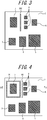
FIG. 3 is a plan view of a wireless communication module according to a first example variation of the embodiment of the present disclosure; -
FIG. 4 is a plan view of a wireless communication module according to a second example variation of the embodiment of the present disclosure; and -
FIG. 5 is a cross-sectional view taken from line B-B ofFIG. 4 . - Conventionally, improvements in the performance of wireless communication modules are desired. The present disclosure aims to provide a wireless communication module with improved performance, and a mobile object equipped with the wireless communication module with the improved performance. According to an embodiment of the present disclosure, the performance of a wireless communication module is improved. Hereinafter, embodiments of the present disclosure will be described with reference to the accompanying drawings.
- A
wireless communication module 1 according to an embodiment of the present disclosure will be described with reference toFIG. 1 . Thewireless communication module 1 is used to perform wireless communication. Thewireless communication module 1 may be provided to any apparatus that performs wireless communication. For example, thewireless communication module 1 may be provided to a mobile object. - The term "mobile object" used herein may encompass, for example, vehicles, ships, and aircraft. Vehicles may include automobiles and industrial vehicles. Vehicles are not limited thereto but may include rail vehicles, domestic vehicles, and fixed-wing aircraft that travel on a runway. Automobiles may include, for example, cars, trucks, buses, motorcycles, and trolley buses. Automobiles are not limited thereto but may include other automobiles that travel on the road. Industrial vehicles may include, for example, agricultural vehicles and construction vehicles. Industrial vehicles may include, for example, forklifts and golf carts. Industrial vehicles for agricultural purpose may include, for example, tractors, tillers, transplanters, binders, combined harvesters, and lawn mowers. Industrial vehicles for construction purposes may include, for example, bulldozers, scrapers, excavators, crane trucks, dump trucks, and load rollers. The vehicles may include human-power vehicles traveling on human power. Classification of the vehicles is not limited to the above. For example, vehicles may include industrial vehicles authorized to travel on the road, and a plurality of categories may include the same type of vehicle. Ships may include, for example, watercrafts, boats, and tankers. Aircraft may include, for example, fixed wing aircraft and rotorcraft.
- The
wireless communication module 1 includes any appropriate components used for wireless communication. For example, thewireless communication module 1 includes asubstrate 2, apower source IC 3, amemory 4, a baseband IC (Integrated Circuit) 5, an RF (Radio Frequency) IC 6, apower amplifier 7, afilter 8, and ashield 9. Thewireless communication module 1 may include any number of each of thepower source IC 3, thememory 4, the baseband IC 5, the RFIC 6, thepower amplifier 7, thefilter 8, and theshield 9. Hereinafter, thepower amplifier 7 will also be referred to as a first element. Thefilter 8 will also be referred to as a second element. - The
substrate 2 is a layered substrate comprising a plurality of layers. Thesubstrate 2 includes, for example, one or more ground layers and one or more insulating layers. However, this is not restrictive. For example, inFIG. 2 thesubstrate 2 is illustrated as including threeground layers insulating layers ground layer 21 is a surface layer, and theground layer 23 is an inner layer. The one or more ground layers that include theground layer 21 serving as the surface layer has agroove 26. The number of the ground layers having thegroove 26 may be appropriately determined. Thegroove 26 will be described in detail below. - The power source IC 3 illustrated in
FIG. 1 supplies electrical power to each constituent element of thewireless communication module 1. - The
memory 4 stores information and programs used for operation of thewireless communication module 1. Thememory 4 may include, for example, a semiconductor memory, a magnetic memory, or an optical memory. The semiconductor memory may include a volatile memory or a nonvolatile memory. - The
baseband IC 5 processes a baseband signal. For example, thebaseband IC 5 inputs a baseband signal to theRFIC 6. Thebaseband IC 5 acquires a baseband signal from theRFIC 6. - The
RFIC 6 processes an RF signal. For example, theRFIC 6 generates an RF signal by modulating a baseband signal input from thebaseband IC 5. TheRFIC 6 inputs the generated RF signal to thepower amplifier 7. TheRFIC 6 acquires, for example, an RF signal input from any appropriate antenna element. - The
power amplifier 7 amplifies the RF signal input from theRFIC 6. Thepower amplifier 7 inputs the amplified RF signal to thefilter 8. - The
filter 8 attenuates a harmonic component of the RF signal amplified by thepower amplifier 7. The RF signal having passed through thefilter 8 is input to any appropriate antenna element. - The
shield 9 attenuates electromagnetic waves radiated from thewireless communication module 1. For example, electromagnetic waves radiated from thewireless communication module 1 may include unnecessary radiation radiated from thepower amplifier 7. Theshield 9 may be formed from any appropriate metallic material. Theshield 9 will be described in detail below. - The
power source IC 3, thememory 4, thebaseband IC 5, theRFIC 6, thepower amplifier 7, thefilter 8, and theshield 9 described above are arranged on theground layer 21 of thesubstrate 2. - The constituent elements of the
wireless communication module 1 are not limited to those described above by way of example. For example, thewireless communication module 1 may further includes any appropriate antenna element. - The
groove 26 will be described in detail. At least a portion of thegroove 26 is located between thepower amplifier 7 and thefilter 8. According to the present embodiment, thegroove 26 may surround thepower amplifier 7. In each of the one or more ground layers having thegroove 26, an inner portion surrounded by thegroove 26 and an outer portion are electrically isolated. In the present embodiment, thepower amplifier 7 is grounded to the inner portion of the one or more ground layers having thegroove 26. On the other hand, thepower source IC 3, thememory 4, thebaseband IC 5, theRFIC 6, thefilter 8, and theshield 9 are grounded to the outer portion of the one or more ground layers having thegroove 26. - The
shield 9 will be described in detail. Theshield 9 is grounded to the outer portion of the one or more ground layers having thegroove 26, as described above. At least a portion of theshield 9 is positioned between thepower amplifier 7 and thefilter 8. According to the present embodiment, theshield 9 may cover thepower amplifier 7. - In the
wireless communication module 1 of the present embodiment, one or more ground layers of thesubstrate 2 has thegroove 26, as described above. Thus, thewireless communication module 1 with improved performance can be realized, as described below. - For example, if the harmonic component of the RF signal amplified by the
power amplifier 7 propagates through the ground and penetrates another element, it may cause trouble such that the element stops its normal operation. For example, if the harmonic component of the RF signal propagates through the ground and penetrates thefilter 8, it may cause trouble by hindering attenuation of the harmonic component of the RF signal by thefilter 8. - As such, the
groove 26 electrically separates the ground to which thepower amplifier 7 is grounded and the ground to which thepower source IC 3, thememory 4, thebaseband IC 5, theRFIC 6, thefilter 8, and theshield 9 are grounded from each other, in the present embodiment. Thus, the harmonic component of the RF signal amplified by thepower amplifier 7 is unlikely to penetrate other elements through the ground. Thus, the likelihood that the trouble described above occurs is reduced. Accordingly, thewireless communication module 1 with improved performance can be realized. - In the
wireless communication module 1 according to the present embodiment, theshield 9 is grounded to a ground separated from thepower amplifier 7. Thus, thewireless communication module 1 with further improved performance can be realized, as described below. - For example, if unnecessary radiation such as a harmonic component of the RF signal amplified by the
power amplifier 7 propagates through the air and penetrates another element, it may cause trouble such that the element stops its normal operation. To reduce penetration of unnecessary radiation, it may be conceived, for example, to cover thepower amplifier 7 with a component such as a shielding cover. However, in cases in which the shield cover is grounded to the same ground to which thepower amplifier 7 is grounded, the harmonic components of the RF signal amplified by thepower amplifier 7 may propagate through the ground and then to the shielding cover. In this case, unnecessary radiation may be radiated from the shielding cover itself. Thus, unnecessary radiation is not necessarily sufficiently reduced. - According to the present embodiment, in contrast, the
shield 9 is grounded to a ground which is separated from thepower amplifier 7. This reduces the likelihood that theshield 9 itself radiates unnecessary radiation. Thus, thewireless communication module 1 with further improved performance can be realized. - Although the present disclosure has been described based on the figures and embodiments, it should be appreciated that those who are skilled in the art may easily perform variations or alteration based on the present disclosure. Accordingly, such variations and alterations are to be included in the scope of the present disclosure. For example, the functions included in each of the means or steps may be rearranged avoiding a logical inconsistency, such that a plurality of means or steps are combined or subdivided.
- For example, in the embodiment described above, the configuration in which the
groove 26 surrounds thepower amplifier 7 has been described. However, a configuration in which thegroove 26 does not surround thepower amplifier 7 is also viable. For example, thewireless communication module 1 may have a configuration in which agroove 260 is provided between thepower amplifier 7 and thefilter 8 as illustrated inFIG. 3 . This configuration also reduces the likelihood that the harmonic components of the RF signal amplified by thepower amplifier 7 propagate through the ground and penetrate another element. Thus, thewireless communication module 1 with improved performance can be realized. - In the embodiment described above, the configuration in which the
shield 9 surrounds thepower amplifier 7 has been described. However, a configuration in which theshield 9 does not surround thepower amplifier 7 is also viable. For example, thewireless communication module 1 may have a configuration in which ashield 90 is provided between thepower amplifier 7 and thefilter 8 as illustrated inFIG. 4 andFIG. 5 . This configuration also reduces the likelihood that the harmonic components of the RF signal amplified by thepower amplifier 7 propagate through the ground and penetrate another element. Thus, thewireless communication module 1 with improved performance can be realized. - Although in the above embodiments configurations in which the
wireless communication module 1 is provided to a mobile object and serves as an apparatus for performing wireless communication has been described, this is not restrictive. Thewireless communication module 1 may be provided to a communication apparatus such as, for example, a mobile phone, a smartphone, a tablet, an IoT (Internet of Things) device, or the like. - The
groove 26 may be formed by cutting out a part of a wiring after laminating the ground layer, or may be a gap formed as a result of lamination (printing) of the ground layer having a wiring pattern in which a gap is formed in a part of the wiring. Thegroove 26 described above may also be referred to as aslit 26, as appropriate. -
- 1
- wireless communication module
- 2
- substrate
- 21, 23, 25
- ground layer
- 22, 24
- insulating layer
- 26
- groove
- 3
- power source IC
- 4
- memory
- 5
- baseband IC
- 6
- RFIC
- 7
- power amplifier
- 8
- filter
- 9, 90
- shield
Claims (7)
- A mobile object comprising
a wireless communication module that includes:a substrate that includes one or more ground layers;a first element that is arranged on the substrate and configured to amplify an input RF signal; anda second element that is arranged on the substrate and is different from the first element,wherein the one or more ground layers include a groove formed between the first element and the second element. - A wireless communication module comprising:a substrate that includes one or more ground layers;a first element that is arranged on the substrate and configured to amplify an input RF signal; anda second element that is arranged on the substrate and is different from the first element,wherein the one or more ground layers include a groove formed between the first element and the second element.
- The wireless communication module according to claim 2,
wherein the one or more ground layers include a first ground layer serving as a surface layer on which the first element is arranged, and a second ground layer serving as an inner layer. - The wireless communication module according to claim 2 or 3,
wherein the groove surrounds the first element, and
in each of the one or more ground layers, an inner portion surrounded by the groove and an outer portion are electrically separated. - The wireless communication module according to claim 4,
wherein the first element is connected to the inner portion of the one or more ground layers, and
the second element is connected to the outer portion of the one or more ground layers. - The wireless communication module according to claim 4 or 5, further comprising a shield that is connected to the outer portion of the one or more ground layers.
- The wireless communication module according to claim 6,
wherein the first element is covered by the shield.
Applications Claiming Priority (2)
| Application Number | Priority Date | Filing Date | Title |
|---|---|---|---|
| JP2017105042A JP6914731B2 (en) | 2017-05-26 | 2017-05-26 | Mobile and wireless communication modules |
| PCT/JP2018/018816 WO2018216557A1 (en) | 2017-05-26 | 2018-05-15 | Mobile body and wireless communication module |
Publications (3)
| Publication Number | Publication Date |
|---|---|
| EP3633862A1 true EP3633862A1 (en) | 2020-04-08 |
| EP3633862A4 EP3633862A4 (en) | 2020-12-16 |
| EP3633862B1 EP3633862B1 (en) | 2022-05-11 |
Family
ID=64396761
Family Applications (1)
| Application Number | Title | Priority Date | Filing Date |
|---|---|---|---|
| EP18806360.6A Active EP3633862B1 (en) | 2017-05-26 | 2018-05-15 | Mobile body and wireless communication module |
Country Status (5)
| Country | Link |
|---|---|
| US (1) | US11024591B2 (en) |
| EP (1) | EP3633862B1 (en) |
| JP (1) | JP6914731B2 (en) |
| CN (1) | CN110663192B (en) |
| WO (1) | WO2018216557A1 (en) |
Family Cites Families (14)
| Publication number | Priority date | Publication date | Assignee | Title |
|---|---|---|---|---|
| JP2003100989A (en) * | 2001-09-27 | 2003-04-04 | Hitachi Ltd | High frequency module |
| CN100421352C (en) * | 2003-06-10 | 2008-09-24 | 株式会社东芝 | High Frequency Power Amplifier Module |
| JP2005094405A (en) * | 2003-09-18 | 2005-04-07 | Tdk Corp | High-frequency module having surface acoustic wave filter |
| JP4105122B2 (en) * | 2004-05-31 | 2008-06-25 | 東光株式会社 | High frequency module |
| JP2010165728A (en) * | 2009-01-13 | 2010-07-29 | Kyocera Corp | Multilayer substrate and portable communication device |
| JP2010225620A (en) * | 2009-03-19 | 2010-10-07 | Panasonic Corp | Circuit module |
| JP4542194B2 (en) * | 2009-09-24 | 2010-09-08 | ルネサスエレクトロニクス株式会社 | High frequency circuit module |
| JP2011187677A (en) * | 2010-03-09 | 2011-09-22 | Panasonic Corp | Module |
| JP2012019091A (en) * | 2010-07-08 | 2012-01-26 | Sony Corp | Module and portable terminal |
| JP2013222829A (en) * | 2012-04-17 | 2013-10-28 | Taiyo Yuden Co Ltd | Circuit module and manufacturing method thereof |
| US9160825B2 (en) * | 2013-10-30 | 2015-10-13 | Taiyo Yuden Co., Ltd. | Communication module |
| JP6300008B2 (en) | 2014-01-28 | 2018-03-28 | 日本精機株式会社 | Vehicle display device |
| CN107078405B (en) * | 2014-10-20 | 2021-03-05 | 株式会社村田制作所 | Wireless communication module |
| US20200203287A1 (en) * | 2018-12-20 | 2020-06-25 | Qualcomm Incorporated | Device comprising compartmental shielding with improved heat dissipation and routing |
-
2017
- 2017-05-26 JP JP2017105042A patent/JP6914731B2/en active Active
-
2018
- 2018-05-15 EP EP18806360.6A patent/EP3633862B1/en active Active
- 2018-05-15 US US16/615,783 patent/US11024591B2/en active Active
- 2018-05-15 WO PCT/JP2018/018816 patent/WO2018216557A1/en not_active Ceased
- 2018-05-15 CN CN201880033999.6A patent/CN110663192B/en active Active
Also Published As
| Publication number | Publication date |
|---|---|
| JP6914731B2 (en) | 2021-08-04 |
| WO2018216557A1 (en) | 2018-11-29 |
| EP3633862B1 (en) | 2022-05-11 |
| CN110663192B (en) | 2021-05-25 |
| CN110663192A (en) | 2020-01-07 |
| JP2018201131A (en) | 2018-12-20 |
| US20200219829A1 (en) | 2020-07-09 |
| EP3633862A4 (en) | 2020-12-16 |
| US11024591B2 (en) | 2021-06-01 |
Similar Documents
| Publication | Publication Date | Title |
|---|---|---|
| JP6009062B2 (en) | Antenna module having a transmitting antenna member and a receiving antenna member | |
| US9502753B2 (en) | Communication terminal device | |
| US20120068896A1 (en) | Microwave antenna assemblies | |
| US10811760B2 (en) | Multi-band window antenna | |
| KR101241484B1 (en) | Feedthrough method and system thereof for radio frequency signal for shielded aircraft fuselage | |
| US10381704B2 (en) | Embedded broadband glass coplanar waveguide coupler | |
| EP3432418B1 (en) | Antenna modules for vehicles | |
| US10080202B2 (en) | Device, method, and computer program for a transceiver system | |
| US11024591B2 (en) | Mobile object and wireless communication module | |
| US12009582B2 (en) | Antenna module and vehicle roof with antenna module | |
| CN105431977B (en) | Antenna system | |
| JP2019062372A (en) | Composite antenna device | |
| US20230178880A1 (en) | Vehicle and antenna apparatus for vehicle | |
| EP4369567A3 (en) | Wireless charging modules including optimized near-field communication (nfc) antennas | |
| US11949154B2 (en) | Antenna device for vehicle | |
| US20150080041A1 (en) | Communication Device for Rail Vehicle, Rail Vehicle Equipped with said Device | |
| US10624247B2 (en) | Circuit board, electronic control unit, and switching control method of electronic control unit | |
| US9935672B2 (en) | Millimetre wave circuit | |
| JP2004129138A (en) | Antenna mounting method, antenna mounting structure, and monitor device | |
| US11056776B2 (en) | Antenna arrangement for a vehicle | |
| JP2018198374A (en) | Mobile body and radio communication module | |
| DE102024117375A1 (en) | Broadband spiral antenna system for a vehicle | |
| WO2018216447A1 (en) | Mobile body, circuit module, wireless communication module, and excess radiation countermeasure method | |
| US20190341681A1 (en) | Multiband antenna device integrated with a housing such as a vehicle multimedia system | |
| BİLGİC | TPMS receive antenna design for large vehicles |
Legal Events
| Date | Code | Title | Description |
|---|---|---|---|
| STAA | Information on the status of an ep patent application or granted ep patent |
Free format text: STATUS: THE INTERNATIONAL PUBLICATION HAS BEEN MADE |
|
| PUAI | Public reference made under article 153(3) epc to a published international application that has entered the european phase |
Free format text: ORIGINAL CODE: 0009012 |
|
| STAA | Information on the status of an ep patent application or granted ep patent |
Free format text: STATUS: REQUEST FOR EXAMINATION WAS MADE |
|
| 17P | Request for examination filed |
Effective date: 20191126 |
|
| AK | Designated contracting states |
Kind code of ref document: A1 Designated state(s): AL AT BE BG CH CY CZ DE DK EE ES FI FR GB GR HR HU IE IS IT LI LT LU LV MC MK MT NL NO PL PT RO RS SE SI SK SM TR |
|
| AX | Request for extension of the european patent |
Extension state: BA ME |
|
| DAV | Request for validation of the european patent (deleted) | ||
| DAX | Request for extension of the european patent (deleted) | ||
| A4 | Supplementary search report drawn up and despatched |
Effective date: 20201117 |
|
| RIC1 | Information provided on ipc code assigned before grant |
Ipc: H01L 23/00 20060101ALI20201111BHEP Ipc: H05K 9/00 20060101ALI20201111BHEP Ipc: H01L 23/552 20060101ALI20201111BHEP Ipc: H04B 15/04 20060101ALI20201111BHEP Ipc: H04B 1/38 20150101AFI20201111BHEP Ipc: H04B 1/525 20150101ALI20201111BHEP Ipc: H01L 23/538 20060101ALI20201111BHEP |
|
| RIC1 | Information provided on ipc code assigned before grant |
Ipc: H01L 23/538 20060101ALI20211203BHEP Ipc: H05K 9/00 20060101ALI20211203BHEP Ipc: H01L 23/00 20060101ALI20211203BHEP Ipc: H01L 23/552 20060101ALI20211203BHEP Ipc: H04B 1/525 20150101ALI20211203BHEP Ipc: H04B 15/04 20060101ALI20211203BHEP Ipc: H04B 1/38 20150101AFI20211203BHEP |
|
| GRAP | Despatch of communication of intention to grant a patent |
Free format text: ORIGINAL CODE: EPIDOSNIGR1 |
|
| STAA | Information on the status of an ep patent application or granted ep patent |
Free format text: STATUS: GRANT OF PATENT IS INTENDED |
|
| INTG | Intention to grant announced |
Effective date: 20220119 |
|
| GRAS | Grant fee paid |
Free format text: ORIGINAL CODE: EPIDOSNIGR3 |
|
| GRAA | (expected) grant |
Free format text: ORIGINAL CODE: 0009210 |
|
| STAA | Information on the status of an ep patent application or granted ep patent |
Free format text: STATUS: THE PATENT HAS BEEN GRANTED |
|
| AK | Designated contracting states |
Kind code of ref document: B1 Designated state(s): AL AT BE BG CH CY CZ DE DK EE ES FI FR GB GR HR HU IE IS IT LI LT LU LV MC MK MT NL NO PL PT RO RS SE SI SK SM TR |
|
| REG | Reference to a national code |
Ref country code: GB Ref legal event code: FG4D |
|
| REG | Reference to a national code |
Ref country code: CH Ref legal event code: EP |
|
| REG | Reference to a national code |
Ref country code: AT Ref legal event code: REF Ref document number: 1492365 Country of ref document: AT Kind code of ref document: T Effective date: 20220515 |
|
| REG | Reference to a national code |
Ref country code: DE Ref legal event code: R096 Ref document number: 602018035539 Country of ref document: DE |
|
| REG | Reference to a national code |
Ref country code: IE Ref legal event code: FG4D |
|
| REG | Reference to a national code |
Ref country code: LT Ref legal event code: MG9D |
|
| REG | Reference to a national code |
Ref country code: NL Ref legal event code: MP Effective date: 20220511 |
|
| REG | Reference to a national code |
Ref country code: AT Ref legal event code: MK05 Ref document number: 1492365 Country of ref document: AT Kind code of ref document: T Effective date: 20220511 |
|
| PG25 | Lapsed in a contracting state [announced via postgrant information from national office to epo] |
Ref country code: SE Free format text: LAPSE BECAUSE OF FAILURE TO SUBMIT A TRANSLATION OF THE DESCRIPTION OR TO PAY THE FEE WITHIN THE PRESCRIBED TIME-LIMIT Effective date: 20220511 Ref country code: PT Free format text: LAPSE BECAUSE OF FAILURE TO SUBMIT A TRANSLATION OF THE DESCRIPTION OR TO PAY THE FEE WITHIN THE PRESCRIBED TIME-LIMIT Effective date: 20220912 Ref country code: NO Free format text: LAPSE BECAUSE OF FAILURE TO SUBMIT A TRANSLATION OF THE DESCRIPTION OR TO PAY THE FEE WITHIN THE PRESCRIBED TIME-LIMIT Effective date: 20220811 Ref country code: NL Free format text: LAPSE BECAUSE OF FAILURE TO SUBMIT A TRANSLATION OF THE DESCRIPTION OR TO PAY THE FEE WITHIN THE PRESCRIBED TIME-LIMIT Effective date: 20220511 Ref country code: LT Free format text: LAPSE BECAUSE OF FAILURE TO SUBMIT A TRANSLATION OF THE DESCRIPTION OR TO PAY THE FEE WITHIN THE PRESCRIBED TIME-LIMIT Effective date: 20220511 Ref country code: HR Free format text: LAPSE BECAUSE OF FAILURE TO SUBMIT A TRANSLATION OF THE DESCRIPTION OR TO PAY THE FEE WITHIN THE PRESCRIBED TIME-LIMIT Effective date: 20220511 Ref country code: GR Free format text: LAPSE BECAUSE OF FAILURE TO SUBMIT A TRANSLATION OF THE DESCRIPTION OR TO PAY THE FEE WITHIN THE PRESCRIBED TIME-LIMIT Effective date: 20220812 Ref country code: FI Free format text: LAPSE BECAUSE OF FAILURE TO SUBMIT A TRANSLATION OF THE DESCRIPTION OR TO PAY THE FEE WITHIN THE PRESCRIBED TIME-LIMIT Effective date: 20220511 Ref country code: ES Free format text: LAPSE BECAUSE OF FAILURE TO SUBMIT A TRANSLATION OF THE DESCRIPTION OR TO PAY THE FEE WITHIN THE PRESCRIBED TIME-LIMIT Effective date: 20220511 Ref country code: BG Free format text: LAPSE BECAUSE OF FAILURE TO SUBMIT A TRANSLATION OF THE DESCRIPTION OR TO PAY THE FEE WITHIN THE PRESCRIBED TIME-LIMIT Effective date: 20220811 Ref country code: AT Free format text: LAPSE BECAUSE OF FAILURE TO SUBMIT A TRANSLATION OF THE DESCRIPTION OR TO PAY THE FEE WITHIN THE PRESCRIBED TIME-LIMIT Effective date: 20220511 |
|
| PG25 | Lapsed in a contracting state [announced via postgrant information from national office to epo] |
Ref country code: RS Free format text: LAPSE BECAUSE OF FAILURE TO SUBMIT A TRANSLATION OF THE DESCRIPTION OR TO PAY THE FEE WITHIN THE PRESCRIBED TIME-LIMIT Effective date: 20220511 Ref country code: PL Free format text: LAPSE BECAUSE OF FAILURE TO SUBMIT A TRANSLATION OF THE DESCRIPTION OR TO PAY THE FEE WITHIN THE PRESCRIBED TIME-LIMIT Effective date: 20220511 Ref country code: LV Free format text: LAPSE BECAUSE OF FAILURE TO SUBMIT A TRANSLATION OF THE DESCRIPTION OR TO PAY THE FEE WITHIN THE PRESCRIBED TIME-LIMIT Effective date: 20220511 Ref country code: IS Free format text: LAPSE BECAUSE OF FAILURE TO SUBMIT A TRANSLATION OF THE DESCRIPTION OR TO PAY THE FEE WITHIN THE PRESCRIBED TIME-LIMIT Effective date: 20220911 |
|
| REG | Reference to a national code |
Ref country code: CH Ref legal event code: PL |
|
| REG | Reference to a national code |
Ref country code: BE Ref legal event code: MM Effective date: 20220531 |
|
| PG25 | Lapsed in a contracting state [announced via postgrant information from national office to epo] |
Ref country code: SM Free format text: LAPSE BECAUSE OF FAILURE TO SUBMIT A TRANSLATION OF THE DESCRIPTION OR TO PAY THE FEE WITHIN THE PRESCRIBED TIME-LIMIT Effective date: 20220511 Ref country code: SK Free format text: LAPSE BECAUSE OF FAILURE TO SUBMIT A TRANSLATION OF THE DESCRIPTION OR TO PAY THE FEE WITHIN THE PRESCRIBED TIME-LIMIT Effective date: 20220511 Ref country code: RO Free format text: LAPSE BECAUSE OF FAILURE TO SUBMIT A TRANSLATION OF THE DESCRIPTION OR TO PAY THE FEE WITHIN THE PRESCRIBED TIME-LIMIT Effective date: 20220511 Ref country code: LU Free format text: LAPSE BECAUSE OF NON-PAYMENT OF DUE FEES Effective date: 20220515 Ref country code: LI Free format text: LAPSE BECAUSE OF NON-PAYMENT OF DUE FEES Effective date: 20220531 Ref country code: EE Free format text: LAPSE BECAUSE OF FAILURE TO SUBMIT A TRANSLATION OF THE DESCRIPTION OR TO PAY THE FEE WITHIN THE PRESCRIBED TIME-LIMIT Effective date: 20220511 Ref country code: DK Free format text: LAPSE BECAUSE OF FAILURE TO SUBMIT A TRANSLATION OF THE DESCRIPTION OR TO PAY THE FEE WITHIN THE PRESCRIBED TIME-LIMIT Effective date: 20220511 Ref country code: CZ Free format text: LAPSE BECAUSE OF FAILURE TO SUBMIT A TRANSLATION OF THE DESCRIPTION OR TO PAY THE FEE WITHIN THE PRESCRIBED TIME-LIMIT Effective date: 20220511 Ref country code: CH Free format text: LAPSE BECAUSE OF NON-PAYMENT OF DUE FEES Effective date: 20220531 |
|
| REG | Reference to a national code |
Ref country code: DE Ref legal event code: R097 Ref document number: 602018035539 Country of ref document: DE |
|
| PG25 | Lapsed in a contracting state [announced via postgrant information from national office to epo] |
Ref country code: MC Free format text: LAPSE BECAUSE OF FAILURE TO SUBMIT A TRANSLATION OF THE DESCRIPTION OR TO PAY THE FEE WITHIN THE PRESCRIBED TIME-LIMIT Effective date: 20220511 |
|
| PLBE | No opposition filed within time limit |
Free format text: ORIGINAL CODE: 0009261 |
|
| STAA | Information on the status of an ep patent application or granted ep patent |
Free format text: STATUS: NO OPPOSITION FILED WITHIN TIME LIMIT |
|
| PG25 | Lapsed in a contracting state [announced via postgrant information from national office to epo] |
Ref country code: AL Free format text: LAPSE BECAUSE OF FAILURE TO SUBMIT A TRANSLATION OF THE DESCRIPTION OR TO PAY THE FEE WITHIN THE PRESCRIBED TIME-LIMIT Effective date: 20220511 |
|
| 26N | No opposition filed |
Effective date: 20230214 |
|
| PG25 | Lapsed in a contracting state [announced via postgrant information from national office to epo] |
Ref country code: IE Free format text: LAPSE BECAUSE OF NON-PAYMENT OF DUE FEES Effective date: 20220515 |
|
| PG25 | Lapsed in a contracting state [announced via postgrant information from national office to epo] |
Ref country code: SI Free format text: LAPSE BECAUSE OF FAILURE TO SUBMIT A TRANSLATION OF THE DESCRIPTION OR TO PAY THE FEE WITHIN THE PRESCRIBED TIME-LIMIT Effective date: 20220511 Ref country code: BE Free format text: LAPSE BECAUSE OF NON-PAYMENT OF DUE FEES Effective date: 20220531 |
|
| P01 | Opt-out of the competence of the unified patent court (upc) registered |
Effective date: 20230508 |
|
| PG25 | Lapsed in a contracting state [announced via postgrant information from national office to epo] |
Ref country code: IT Free format text: LAPSE BECAUSE OF FAILURE TO SUBMIT A TRANSLATION OF THE DESCRIPTION OR TO PAY THE FEE WITHIN THE PRESCRIBED TIME-LIMIT Effective date: 20220511 |
|
| PG25 | Lapsed in a contracting state [announced via postgrant information from national office to epo] |
Ref country code: MK Free format text: LAPSE BECAUSE OF FAILURE TO SUBMIT A TRANSLATION OF THE DESCRIPTION OR TO PAY THE FEE WITHIN THE PRESCRIBED TIME-LIMIT Effective date: 20220511 Ref country code: CY Free format text: LAPSE BECAUSE OF FAILURE TO SUBMIT A TRANSLATION OF THE DESCRIPTION OR TO PAY THE FEE WITHIN THE PRESCRIBED TIME-LIMIT Effective date: 20220511 |
|
| PG25 | Lapsed in a contracting state [announced via postgrant information from national office to epo] |
Ref country code: HU Free format text: LAPSE BECAUSE OF FAILURE TO SUBMIT A TRANSLATION OF THE DESCRIPTION OR TO PAY THE FEE WITHIN THE PRESCRIBED TIME-LIMIT; INVALID AB INITIO Effective date: 20180515 |
|
| PG25 | Lapsed in a contracting state [announced via postgrant information from national office to epo] |
Ref country code: TR Free format text: LAPSE BECAUSE OF FAILURE TO SUBMIT A TRANSLATION OF THE DESCRIPTION OR TO PAY THE FEE WITHIN THE PRESCRIBED TIME-LIMIT Effective date: 20220511 |
|
| PG25 | Lapsed in a contracting state [announced via postgrant information from national office to epo] |
Ref country code: MT Free format text: LAPSE BECAUSE OF FAILURE TO SUBMIT A TRANSLATION OF THE DESCRIPTION OR TO PAY THE FEE WITHIN THE PRESCRIBED TIME-LIMIT Effective date: 20220511 |
|
| PG25 | Lapsed in a contracting state [announced via postgrant information from national office to epo] |
Ref country code: BG Free format text: LAPSE BECAUSE OF FAILURE TO SUBMIT A TRANSLATION OF THE DESCRIPTION OR TO PAY THE FEE WITHIN THE PRESCRIBED TIME-LIMIT Effective date: 20220511 |
|
| PG25 | Lapsed in a contracting state [announced via postgrant information from national office to epo] |
Ref country code: BG Free format text: LAPSE BECAUSE OF FAILURE TO SUBMIT A TRANSLATION OF THE DESCRIPTION OR TO PAY THE FEE WITHIN THE PRESCRIBED TIME-LIMIT Effective date: 20220511 |
|
| PGFP | Annual fee paid to national office [announced via postgrant information from national office to epo] |
Ref country code: GB Payment date: 20250327 Year of fee payment: 8 |
|
| PGFP | Annual fee paid to national office [announced via postgrant information from national office to epo] |
Ref country code: DE Payment date: 20250402 Year of fee payment: 8 |
|
| PGFP | Annual fee paid to national office [announced via postgrant information from national office to epo] |
Ref country code: FR Payment date: 20250401 Year of fee payment: 8 |