EP3633082A1 - Nitride single crystal - Google Patents
Nitride single crystal Download PDFInfo
- Publication number
- EP3633082A1 EP3633082A1 EP18806724.3A EP18806724A EP3633082A1 EP 3633082 A1 EP3633082 A1 EP 3633082A1 EP 18806724 A EP18806724 A EP 18806724A EP 3633082 A1 EP3633082 A1 EP 3633082A1
- Authority
- EP
- European Patent Office
- Prior art keywords
- single crystal
- nitride single
- crystal
- nitride
- solvent
- Prior art date
- Legal status (The legal status is an assumption and is not a legal conclusion. Google has not performed a legal analysis and makes no representation as to the accuracy of the status listed.)
- Withdrawn
Links
Images

Classifications
-
- C—CHEMISTRY; METALLURGY
- C30—CRYSTAL GROWTH
- C30B—SINGLE-CRYSTAL GROWTH; UNIDIRECTIONAL SOLIDIFICATION OF EUTECTIC MATERIAL OR UNIDIRECTIONAL DEMIXING OF EUTECTOID MATERIAL; REFINING BY ZONE-MELTING OF MATERIAL; PRODUCTION OF A HOMOGENEOUS POLYCRYSTALLINE MATERIAL WITH DEFINED STRUCTURE; SINGLE CRYSTALS OR HOMOGENEOUS POLYCRYSTALLINE MATERIAL WITH DEFINED STRUCTURE; AFTER-TREATMENT OF SINGLE CRYSTALS OR A HOMOGENEOUS POLYCRYSTALLINE MATERIAL WITH DEFINED STRUCTURE; APPARATUS THEREFOR
- C30B29/00—Single crystals or homogeneous polycrystalline material with defined structure characterised by the material or by their shape
- C30B29/10—Inorganic compounds or compositions
- C30B29/40—AIIIBV compounds wherein A is B, Al, Ga, In or Tl and B is N, P, As, Sb or Bi
- C30B29/403—AIII-nitrides
-
- C—CHEMISTRY; METALLURGY
- C30—CRYSTAL GROWTH
- C30B—SINGLE-CRYSTAL GROWTH; UNIDIRECTIONAL SOLIDIFICATION OF EUTECTIC MATERIAL OR UNIDIRECTIONAL DEMIXING OF EUTECTOID MATERIAL; REFINING BY ZONE-MELTING OF MATERIAL; PRODUCTION OF A HOMOGENEOUS POLYCRYSTALLINE MATERIAL WITH DEFINED STRUCTURE; SINGLE CRYSTALS OR HOMOGENEOUS POLYCRYSTALLINE MATERIAL WITH DEFINED STRUCTURE; AFTER-TREATMENT OF SINGLE CRYSTALS OR A HOMOGENEOUS POLYCRYSTALLINE MATERIAL WITH DEFINED STRUCTURE; APPARATUS THEREFOR
- C30B9/00—Single-crystal growth from melt solutions using molten solvents
- C30B9/04—Single-crystal growth from melt solutions using molten solvents by cooling of the solution
- C30B9/08—Single-crystal growth from melt solutions using molten solvents by cooling of the solution using other solvents
- C30B9/10—Metal solvents
Definitions
- the present invention relates to a nitride single crystal.
- Nitride single crystals (so-called nitride semiconductors) attract attention as materials of light-emitting devices which emit blue to ultraviolet short wavelength light or power transistors. Especially an aluminum nitride single crystal attracts attention as a material of the substrate of an ultraviolet light-emitting device.
- Nitride single crystals are produced, for example, by a vapor phase growth method such as a sublimation method or a halide vapor phase epitaxy (HVPE) method; or a liquid phase growth method such as a flux method (refer to the following Patent Literature 1 to 4).
- a nitride which is a raw material is sublimated at high temperature, and the nitride is deposited on the surface of a seed crystal at low temperature and crystallized. Since the crystal growth rate is high in a sublimation method, the sublimation method is suitable to produce bulk crystals. However, a nitride single crystal is easily colored brown due to surplus deposition of specific atoms or molecules, or the like in the single crystal in the case of a sublimation method, and it is difficult to obtain a nitride single crystal having high crystallinity.
- a nitride is deposited on the surface of a seed crystal and crystallized by reacting a gaseous chloride and ammonia.
- a gaseous chloride and ammonia Although the coloring of the nitride single crystal is suppressed in the case of the halide vapor phase epitaxy method, it is difficult to obtain a nitride single crystal having few defects and high crystallinity.
- a nitride single crystal is grown on the surface of a seed crystal in a liquid phase. According to a flux method, a single crystal having few defects is easily obtained theoretically as compared with the case of the vapor phase growth method.
- Methods for producing a nitride single crystal by a liquid phase epitaxy (LPE) method which is one of flux methods, have been investigated until now.
- LPE liquid phase epitaxy
- the present invention has been completed in light of the above-mentioned situation, and an object of the present invention is to provide a nitride single crystal having high crystallinity.
- a nitride single crystal according to one aspect of the present invention has a wurtzite crystal structure, and a content of boron in the nitride single crystal is 0.5 ppm by mass or more and 251 ppm by mass or less.
- the content of boron in the above-mentioned nitride single crystal may be 1 ppm by mass or more and 52 ppm by mass or less.
- the above-mentioned nitride single crystal may contain at least one element of Group 13.
- the above-mentioned nitride single crystal may contain aluminum.
- the above-mentioned nitride single crystal may be aluminum nitride.
- the above-mentioned nitride single crystal may contain at least one element selected from the group consisting of iron, nickel, titanium, silicon, vanadium, copper, cobalt, manganese and chromium.
- a total content of iron, nickel, titanium, silicon, vanadium, copper, cobalt, manganese and chromium in the above-mentioned nitride single crystal may be 1 ppm by mass or more and 100 ppm by mass or less.
- the above-mentioned nitride single crystal may be a substrate wherein a thickness is 10 ⁇ m or more and 2 mm or less.
- a nitride single crystal having high crystallinity is provided.
- a nitride single crystal 10 has a wurtzite crystal structure.
- the nitride single crystal 10 is called a single crystal of a nitride of an element E (for example, EN).
- the nitride single crystal 10 may contain at least one element of Group 13. That is, the element E shown in (a) in Figure 1 may be at least one element of Group 13.
- the nitride single crystal 10 may be a single crystal of a nitride of at least one element of Group 13.
- the element of Group 13 (element E) contained in the nitride single crystal 10 may be at least one selected from the group consisting of aluminum (Al), gallium (Ga), indium (In) and thallium (T1).
- the nitride single crystal 10 may contain, for example, aluminum as an element of Group 13 (element E).
- the content of boron (B) in the nitride single crystal 10 according to the present embodiment is 0.5 ppm by mass or more and 251 ppm by mass or less.
- the composition of the nitride single crystal 10 may be approximately represented as Al x Ga y In z N. x + y +z is around 1, x is 0 or more and 1 or less, y is 0 or more and 1 or less, and z is 0 or more and 1 or less.
- the nitride single crystal 10 may be, for example, aluminum nitride (AlN).
- the nitride single crystal 10 may be, for example, gallium nitride (GaN).
- the nitride single crystal 10 may be, for example, indium nitride (InN).
- the nitride single crystal 10 may be, for example indium gallium nitride (InGaN).
- a triangular pyramid in which nitrogen atoms or nitrogen ions (anions) are disposed at the four vertices is constituted in the nitride single crystal 10 having a wurtzite crystal structure.
- An atom of a trivalent element E or an ion (cation) of the element E is disposed at the center of this triangular pyramid.
- a triangle in which nitrogen atoms or nitrogen ions are disposed at the three vertices at normal pressure is constituted in a boron nitride single crystal 20 (BN).
- a trivalent boron atom or a boron ion (cation) is disposed at the center of this triangle.
- the radius of a boron atom or a boron ion is smaller than the radius of a nitrogen atom or a nitrogen ion. Therefore, one boron atom or one boron ion fits in a space surrounded by three nitrogen atoms or three nitrogen ions. Consequently, a boron nitride single crystal has a planar hexagonal crystal structure. Since the nitride single crystal 10 according to the present embodiment contains a minute amount of boron, some atoms of the element E shown in (a) of Figure 1 are substituted with boron atoms. The radius of a boron atom or a boron ion is smaller than the radius of an atom of the element E or an ion of the element E.
- a boron atom or a boron ion easily fits in the space surrounded by the four nitrogen atoms or nitrogen ions (the center of the triangular pyramid) as compared with an atom of the element E or an ion of element E in the same way as the case of the boron nitride single crystal. Consequently, in the nitride single crystal 10 containing boron, stress which acts on the crystal lattice is relaxed as compared with a nitride single crystal not containing boron, the distortion of the crystal structure is suppressed, and the crystallinity increases.
- boron can hardly suppress the distortion of the crystal structure. Therefore, the crystallinity of the nitride single crystal wherein the content of boron is less than 0.5 ppm by mass is inferior to the crystallinity of a nitride single crystal wherein the content of boron is 0.5 ppm by mass or more and 251 ppm by mass or less.
- a nitride wherein the content of boron is more than 251 ppm by mass can hardly become a single crystal originally, and easily becomes a polycrystal.
- the surface roughness of the nitride wherein the content of boron is more than 251 ppm by mass is higher than the surface roughness of the nitride single crystal 10 wherein the content of boron is 0.5 ppm by mass or more and 251 ppm by mass or less. Therefore, a crystal of another compound (for example, compound semiconductor) can hardly be formed on the surface of the nitride crystal (polycrystal) wherein the content of boron is more than 251 ppm by mass. That is, the nitride crystal (polycrystal) wherein the content of boron is more than 251 ppm by mass can hardly be used as a substrate of light-emitting devices such as LEDs.
- Improvement in the crystallinity of the nitride single crystal 10 is confirmed by a decrease in the half width of the rocking curve of the nitride single crystal 10 measured by X-ray diffraction (XRD) as mentioned below. It may be confirmed by a pole figure measured by XRD whether a nitride is a single crystal or not. It may be confirmed by in-plane diffractometry whether a nitride is a single crystal or not.
- XRD X-ray diffraction
- the radius of an aluminum atom or an aluminum ion (cation) is smaller than the radius of a gallium atom or a gallium ion, and approximate to the ion radius of a boron atom or a boron ion (cation). Therefore, the distortion of the crystal structure is easily relaxed by inclusion of boron in a nitride single crystal containing aluminum. Especially the distortion of the crystal structure is easily relaxed by inclusion of boron in an aluminum nitride single crystal.
- the content of the boron in the nitride single crystal 10 may be 1 ppm by mass or more and 123 ppm by mass or less, 1 ppm by mass or more and 66 ppm by mass or less, 1 ppm by mass or more and 52 ppm by mass or less, 15 ppm by mass or more and 52 ppm by mass or less, or 20 ppm by mass or more and 52 ppm by mass or less.
- the nitride single crystal 10 easily has high crystallinity. In other words, when the content of boron is in the above-mentioned range, the half width of the rocking curve of the nitride single crystal 10 easily decreases.
- the above-mentioned nitride single crystal 10 may contain at least one element selected from the group consisting of iron (Fe), nickel (Ni), titanium (Ti), silicon (Si), vanadium (V), copper (Cu), cobalt (Co), manganese (Mn) and chromium (Cr). These elements have a different ion radius from elements of Group 13, and, for example, can fit in a wurtzite crystal structure as cations. Consequently, the distortion of the nitride single crystal 10 is further suppressed, and the half width of the rocking curve of the nitride single crystal 10 further decreases. At least one element selected from the group consisting of nickel, titanium, silicon, vanadium, copper, cobalt, manganese and chromium may be derived from, for example, a solvent (flux) used for producing the nitride single crystal 10.
- a solvent fluorescence
- the total content of iron, nickel, titanium, silicon, vanadium, copper, cobalt, manganese and chromium in the nitride single crystal 10 may be 1 ppm by mass or more and 100 ppm by mass or less. In this case, the distortion of the nitride single crystal 10 is further suppressed, and the half width of the rocking curve of the nitride single crystal 10 further decreases. For the same reason, the total content of iron, nickel, titanium, silicon, vanadium, copper, cobalt, manganese and chromium in the nitride single crystal 10 may be 1.3 ppm by mass or more and 59 ppm by mass or less.
- the nitride single crystal 10 may be a substrate wherein the thickness is 10 ⁇ m or more and 2 mm or less.
- a substrate comprising the nitride single crystal 10 is formed by growing the nitride single crystal 10 containing boron on a flat surface of a seed crystal.
- the crystal structure of the single crystal 10 tends to be influenced by the crystal structure of the seed crystal, the crystal structure of the single crystal 10 is easily distorted.
- the thickness of the substrate of single crystal 10 reaches 10 ⁇ m or more with crystal growth, the distortion of the crystal structure tends to be relaxed by inclusion of boron, and the crystallinity of the single crystal 10 easily improves.
- the thickness of the substrate comprising the nitride single crystal 10 may be 2 mm or less to suppress cracks of the substrate resulting from thermal distortion or stress.
- the thickness of the substrate comprising the nitride single crystal 10 may be 11 ⁇ m or more and 1758 ⁇ m or less.
- a method for producing a nitride single crystal 10 may be a flux method, which is a type of liquid phase growth method.
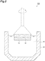
- the method for producing a nitride single crystal 10 may be performed, for example, using a production equipment 100 as shown in Figure 2 .
- the method for producing a nitride single crystal 10 comprises: a step of preparing a solvent 40 containing elements which are raw materials of a nitride (metallic elements such as elements of Group 13) and boron; and a step of feeding nitrogen gas into the solvent 40, contacting the surface of a seed crystal 30 with the solvent 40, and growing a nitride single crystal 10 on the surface of the seed crystal 30. Details of the production method will be described hereinafter.
- the solvent 40 may be called flux.
- the solvent 40 may contain an element of Group 13 such as aluminum, gallium, indium or thallium, and boron as raw materials of the nitride.
- the solvent 40 may contain at least one element selected from the group consisting of nickel, titanium, silicon, vanadium, copper, cobalt, manganese and chromium.
- the content of the boron in the nitride single crystal 10 can be controlled to 0.5 ppm by mass or more and 251 ppm by mass or less by adjusting the content of boron (for example, the number of moles) in the solvent 40 as mentioned below.
- the solvent 40 may be prepared, for example, in the following procedure.
- All of the raw materials of solvent 40 may be simple substances (metal simple substances).
- the raw materials are weighed, and a crucible is charged with the raw materials. All the raw materials in the crucible are heated and melted at 1600 to 1800°C in an inert atmosphere in a vacuum chamber, and all the materials are stirred and mixed.
- a block (metal block) of a mixture of the raw materials is obtained by cooling the mixture of the melted raw materials to room temperature.
- the crucible is charged with the block of the mixture of the raw materials again, the mixture of the raw materials in the crucible 50 is melted in the vacuum chamber, and the mixture of the raw materials is stirred. Consequently, a homogeneous solvent 40 is prepared.
- a nitride single crystal 10 may be grown in the following procedure.
- the temperature of the solvent 40 at the time of stirring the solvent 40 may be, for example, 1500°C or more and 1800°C or less.
- the temperature of the solvent 40 at the time of stirring the solvent 40 is influenced by the structure of the heating part of a production equipment 100 (single crystal growth furnace), the ratio of nitrogen in the mixed gas, and the like. Therefore, the structure of the furnace, the ratio of nitrogen in mixed gas, the output power of the heating part, and the like may be determined so that the temperature of the solvent 40 at the time of stirring the solvent 40 (stirring temperature) is adjusted to a desired and predetermined temperature (the above-mentioned temperature range).
- the solvent 40 is stirred, the temperature of the solvent 40 is then lowered gradually to the saturation temperature, at which a nitride begins to deposit, one surface of the seed crystal 30 is then contacted with the solvent 40 while the surface is rotated in the plane. Consequently, the nitride single crystal 10 begins to grow on the surface of the seed crystal 30.
- the temperature of the solvent 40 in the growth process of the nitride single crystal 10 (the above-mentioned saturation temperature) may be, for example, 1400°C or more and 1750°C or less.
- the temperature of the solvent 40 in the growth process of the nitride single crystal 10 is influenced by the structure of the heating part of the production equipment 100 (single crystal growth furnace), the ratio of nitrogen in the mixed gas, and the like. Therefore, the structure of the heating part of production equipment 100 (single crystal growth furnace), the ratio of the nitrogen in mixed gas, the output power of the heating part, and the like may be determined and adjusted so that the temperature of solvent 40 in the growth process of nitride single crystal 10 be adjusted to a desired and predetermined temperature (saturation temperature) or less. Time for which the nitride single crystal 10 is grown may be, for example, several hours or more and tens of hours or less.
- thermocouple When a high frequency induction heating furnace is used as a single crystal growth furnace, it is difficult to measure the temperature of the solvent 40 in the crucible 50 correctly by a thermocouple. It is because the thermocouple itself generates heat by the action of high frequency in the high frequency induction heating furnace. Therefore, temperature conditions such as stirring temperature and growth temperature may be set and controlled by the repetition of the following experiments (trial and error). First, the output power of the heating part of the high frequency induction heating furnace is increased, and the raw materials in the crucible 50 are heated and melted. The melted raw materials (solvent 40) are stirred and cooled rapidly to room temperature, and it is observed whether undissolved matter on the liquid surface of the solvent 40 exists or not.
- the output power of the heating part is increased until the undissolved matter disappears on the liquid surface of solvent 40.
- the temperature of the solvent 40 heated at an output power at which undissolved matter disappears on the liquid surface of the solvent 40 is the stirring temperature.
- the temperature of the solvent 40 heated at output power at which the nitride single crystal 10 begins to grow is a saturation temperature (starting temperature of crystal growth).
- the stirring temperature and the growth temperature can be indirectly controlled separately by adjusting the output power of the heating part of the high frequency induction heating furnace.
- a solvent does not contain boron
- microcrystals of a nitride easily deposit irregularly in the solvent. Therefore, in the conventional flux method, a nitride single crystal hardly grew on the surface of a seed crystal. Meanwhile, in the present embodiment, since a solvent 40 containing boron is used, the irregular deposition of the microcrystals in the solvent 40 is suppressed, and a nitride single crystal 10 wherein the crystallinity is high easily grows on the surface of a seed crystal 30 as compared with the conventional flux method.
- the nitride single crystal 10 grown in the above procedure is taken out of the solvent 40 with the seed crystal 30 and cooled to room temperature.
- the nitride single crystal 10 is completed by removing metal (flux) adhering to the surface of the single crystal 10 by acid cleaning.
- the seed crystal may be a nitride single crystal.
- a nitride single crystal to be used as a seed crystal may be produced by a method other than the above-mentioned method for producing a nitride single crystal (for example, a sublimation method).
- the seed crystal may be a nitride single crystal of an element of Group 13.
- the seed crystal may be a single crystal of aluminum nitride.
- the seed crystal may be a single crystal of sapphire or a single crystal of silicon carbide.
- the nitride single crystal 10 according to the present embodiment may be used as a substrate which a deep ultraviolet light emitting diode such as a UVC LED or a DUV LED comprises.
- the nitride single crystal 10 may be used as a substrate which a semiconductor laser oscillator of an ultraviolet laser or the like comprises.
- the seed crystal 30 and the nitride single crystal 10 formed on the surface of the seed crystal 30 may be used as one substrate (integrated substrate).
- the nitride single crystal 10 according to an embodiment may be used, for example, for a power transistor.
- the aluminum nitride (AlN) crystal of Example 1 was produced by performing the following steps in a vacuum chamber.
- the simple substances (metal simple substances) of elements shown in the following table 1 were weighed, and a crucible made of alumina was charged with the simple substances. The total mass of the raw materials was adjusted to 250 g. All the raw materials were melted and integrated by mixing all the raw materials in the crucible and heating in an argon atmosphere at 1650°C. A block of a mixture of the raw materials was obtained by cooling the mixture of the melted raw materials to room temperature.
- the crucible made of alumina was charged with the block of the mixture of the raw materials again.
- the block of the mixture of the raw materials in the crucible was melted by heating the block in a high frequency induction heating furnace.
- a homogeneous solvent was obtained by stirring the mixture of the melted raw materials using a tool for stirring provided at the top of the crucible.
- the tool for stirring was made of alumina.
- the molar ratios of the elements in a solvent were adjusted to values shown in the following table 1 by weighing the above-mentioned raw materials (the simple substances of the elements).
- the symbols of elements in brackets ([]) in the following table 1 mean the numbers of moles or the content (unit: % by mol) of the elements in the solvent.
- [Ti] means the number of moles or the content (unit: % by mol) of Ti in the solvent.
- Other symbols of elements in brackets also mean the same.
- a plate-like seed crystal was fixed with a fixture provided at the top of the crucible, and the C surface of the seed crystal was opposed almost parallel to the liquid surface of the solvent.
- As the seed crystal a plate of an aluminum nitride single crystal produced by a sublimation method was used. The size of the seed crystal was 10 mm ⁇ 10 mm ⁇ 0.3 mm.
- the fixture of the seed crystal was also made of alumina.
- the atmospheric pressure in a vacuum chamber was reduced to 0.1 Pa or less by deaeration using a vacuum pump.
- a mixed gas obtained by mixing argon and nitrogen at a ratio (volume ratio) of 8 to 2 was fed into the vacuum chamber after the deaeration in the vacuum chamber, and the atmospheric pressure in the vacuum chamber was adjusted to 0.1 MPa. Then, a small amount of the mixed gas was continuously fed into the vacuum chamber until an AlN crystal grown in the vacuum chamber was taken out of the vacuum chamber.
- the solvent in the crucible was stirred while the solvent was heated at so high a temperature that raw materials (metals) and AlN were dissolved completely using a high frequency induction heating furnace and the tool for stirring. Nitrogen derived from the mixed gas was homogeneously dissolved in the solvent by this heating and stirring, and nitrogen in the solvent was saturated.
- the temperature of the solvent was lowered to a saturation temperature, at which AlN begins to deposit, the C surface of the seed crystal 30 was then contacted on the liquid surface of the solvent 40, and the seed crystal 30 was continuously rotated in the C surface by rotating the fixture.
- An AlN crystal was grown on the C surface of the seed crystal by lowering the temperature of the solvent gradually. The AlN crystal growth was continued until the thickness of the AlN crystal reached a value shown in the following table 2.
- the C surface (surface) of the AlN crystal of Example 1 produced in the above procedure was polished, and the C surface of the crystal was made even. It was confirmed that the AlN crystal grown on the surface of the seed crystal was a single crystal by X-ray diffractometry (2 ⁇ / ⁇ method) and the measurement of a pole figure.
- a rocking curve is the distribution of the intensity of diffracted X-rays measured by fixing 2 ⁇ at the diffraction peak position of the plane (0002) and scanning ⁇ near diffraction conditions.
- 2 ⁇ is an angle which the incidence direction of incident X-rays (CuK ⁇ 1 line) and the detection direction of diffracted X-rays form.
- ⁇ is an incidence angle of the incident X-rays with respect to the (0002) plane (C surface) of the AlN single crystal.
- the half width of the rocking curve of the AlN single crystal (FWHM AlN ) of Example 1 was a value shown in the following table 2.
- a sapphire single crystal produced by edge-defined film-fed growth (EFG) method was used as a standard sample for evaluating the crystallinity of the AlN single crystal as follows. This sapphire single crystal was a plate having the (0006) plane (C surface) direction.
- the rocking curve of the plane (0006) (C surface) of the sapphire single crystal (standard sample) was measured by the same method as the above, and the half width of the rocking curve (FWHM Al2O3 ) was determined.
- the half width ratio of the rocking curve of the AlN single crystal (FWHM AlN /FWHM Al2O3 ) of Example 1 was calculated by dividing the half width of the rocking curve of the AlN single crystal FWHM AlN of Example 1 by the half width of the rocking curve of the sapphire single crystal FWHM Al2O3 .
- the half width ratio (FWHM AlN /FWHM Al2O3 ) is 1.2.
- the AlN single crystal has as good crystal quality as the sapphire single crystal. That is, as the half width ratio of the rocking curve becomes nearer to 1.0, the crystallinity of the AlN single crystal becomes higher.
- the half width ratio of the rocking curve of the AlN single crystal of Example 1 was a value shown in the following table 2.
- the composition of the AlN single crystal of Example 1 growing on the surface of the seed crystal was analyzed by secondary ion mass spectrometry (SIMS) after the above measurement using X-rays. As a result of SIMS, it was confirmed that the single crystal of Example 1 was AlN containing a minute amount of boron.
- the content of each element in the AlN single crystal of Example 1 was measured by SIMS.
- the content of each element in the AlN single crystal of Example 1 was values shown in the following table 2.
- Examples 2 to 11 and Comparative Examples 1 to 3 the simple substances of elements (metal simple substances) shown in the following table 1 were used as the raw materials of each solvent (flux).
- the molar ratio of each element in the solvent was adjusted to values shown in the following table 1.
- the ratio of argon to nitrogen in a mixed gas fed into a vacuum chamber was adjusted to the range of 9 to 1 to 6 to 4.
- the AlN crystals of Examples 2 to 11 and Comparative Examples 1 to 3 were produced individually in the same method as in Example 1 except for these items.
- the half widths of the rocking curves of the AlN single crystals (FWHM AlN ) of Examples 2 to 11 and Comparative Example 1 and 2 were values shown in the following table 2.
- the half width ratios of the rocking curves of the AlN single crystals (FWHM AlN /FWHM Al2O3 ) of Examples 2 to 11 and Comparative Example 1 and 2 were values shown in the following table 2.
- a nitride single crystal according to the present invention is used, for example, as a substrate which light emitting diodes comprise.
- nitride single crystal 10: nitride single crystal, 20: boron nitride single crystal, 30: seed crystal, 40: solution of raw materials, 50: crucible, 100: device for producing nitride single crystal.
Landscapes
- Chemical & Material Sciences (AREA)
- Engineering & Computer Science (AREA)
- Crystallography & Structural Chemistry (AREA)
- Materials Engineering (AREA)
- Metallurgy (AREA)
- Organic Chemistry (AREA)
- Inorganic Chemistry (AREA)
- Crystals, And After-Treatments Of Crystals (AREA)
Abstract
Description
- The present invention relates to a nitride single crystal.
- Nitride single crystals (so-called nitride semiconductors) attract attention as materials of light-emitting devices which emit blue to ultraviolet short wavelength light or power transistors. Especially an aluminum nitride single crystal attracts attention as a material of the substrate of an ultraviolet light-emitting device. Nitride single crystals are produced, for example, by a vapor phase growth method such as a sublimation method or a halide vapor phase epitaxy (HVPE) method; or a liquid phase growth method such as a flux method (refer to the following Patent Literature 1 to 4).
- In a sublimation method described in the following Patent Literature 1 and the like, a nitride which is a raw material is sublimated at high temperature, and the nitride is deposited on the surface of a seed crystal at low temperature and crystallized. Since the crystal growth rate is high in a sublimation method, the sublimation method is suitable to produce bulk crystals. However, a nitride single crystal is easily colored brown due to surplus deposition of specific atoms or molecules, or the like in the single crystal in the case of a sublimation method, and it is difficult to obtain a nitride single crystal having high crystallinity.
- In a halide vapor phase epitaxy method described in the following Patent Literature 2 and the like, a nitride is deposited on the surface of a seed crystal and crystallized by reacting a gaseous chloride and ammonia. Although the coloring of the nitride single crystal is suppressed in the case of the halide vapor phase epitaxy method, it is difficult to obtain a nitride single crystal having few defects and high crystallinity.
- In a flux method described in the following Patent Literature 3 and the like, a nitride single crystal is grown on the surface of a seed crystal in a liquid phase. According to a flux method, a single crystal having few defects is easily obtained theoretically as compared with the case of the vapor phase growth method. Methods for producing a nitride single crystal by a liquid phase epitaxy (LPE) method, which is one of flux methods, have been investigated until now. However, in a conventional liquid phase epitaxy method, a nitride single crystal having high crystallinity has not been obtained.
-
- Patent Literature 1: Japanese Unexamined Patent Publication No.
2013-6740 - Patent Literature 2: Japanese Unexamined Patent Publication No.
2010-89971 - Patent Literature 3: Japanese Unexamined Patent Publication No.
2007-182333 - Patent Literature 4: Japanese Unexamined Patent Publication No.
H8-239752 - The present invention has been completed in light of the above-mentioned situation, and an object of the present invention is to provide a nitride single crystal having high crystallinity.
- A nitride single crystal according to one aspect of the present invention has a wurtzite crystal structure, and a content of boron in the nitride single crystal is 0.5 ppm by mass or more and 251 ppm by mass or less.
- The content of boron in the above-mentioned nitride single crystal may be 1 ppm by mass or more and 52 ppm by mass or less.
- The above-mentioned nitride single crystal may contain at least one element of Group 13.
- The above-mentioned nitride single crystal may contain aluminum.
- The above-mentioned nitride single crystal may be aluminum nitride.
- The above-mentioned nitride single crystal may contain at least one element selected from the group consisting of iron, nickel, titanium, silicon, vanadium, copper, cobalt, manganese and chromium.
- A total content of iron, nickel, titanium, silicon, vanadium, copper, cobalt, manganese and chromium in the above-mentioned nitride single crystal may be 1 ppm by mass or more and 100 ppm by mass or less.
- The above-mentioned nitride single crystal may be a substrate wherein a thickness is 10 µm or more and 2 mm or less.
- According to the present invention, a nitride single crystal having high crystallinity is provided.
-
- [
Figure 1 ] (a) inFigure 1 is a perspective view of a nitride single crystal structure (wurtzite crystal structure) according to one embodiment of the present invention, and (b) inFigure 1 is a perspective view of a boron nitride single crystal (hexagonal crystal) structure. - [
Figure 2] Figure 2 is a schematic diagram showing a method for producing a nitride single crystal according to one embodiment of the present invention. - Suitable embodiments of the present invention will be described with reference to Figures hereinafter depending on the case. However, the present invention is not limited to the following embodiments at all. In Figures, the same or equivalent components are indicated with the same sign.
- As shown in (a) in
Figure 1 , a nitridesingle crystal 10 according to the present embodiment has a wurtzite crystal structure. The nitridesingle crystal 10 is called a single crystal of a nitride of an element E (for example, EN). The nitridesingle crystal 10 may contain at least one element of Group 13. That is, the element E shown in (a) inFigure 1 may be at least one element of Group 13. The nitridesingle crystal 10 may be a single crystal of a nitride of at least one element of Group 13. The element of Group 13 (element E) contained in the nitridesingle crystal 10 may be at least one selected from the group consisting of aluminum (Al), gallium (Ga), indium (In) and thallium (T1). The nitridesingle crystal 10 may contain, for example, aluminum as an element of Group 13 (element E). The content of boron (B) in the nitridesingle crystal 10 according to the present embodiment is 0.5 ppm by mass or more and 251 ppm by mass or less. - Since the content of boron in the nitride
single crystal 10 is very low as mentioned above, the composition of the nitridesingle crystal 10 may be approximately represented as AlxGayInzN. x + y +z is around 1, x is 0 or more and 1 or less, y is 0 or more and 1 or less, and z is 0 or more and 1 or less. The nitridesingle crystal 10 may be, for example, aluminum nitride (AlN). The nitridesingle crystal 10 may be, for example, gallium nitride (GaN). The nitridesingle crystal 10 may be, for example, indium nitride (InN). The nitridesingle crystal 10 may be, for example indium gallium nitride (InGaN). - As shown in (a) in
Figure 1 , a triangular pyramid in which nitrogen atoms or nitrogen ions (anions) are disposed at the four vertices is constituted in the nitridesingle crystal 10 having a wurtzite crystal structure. An atom of a trivalent element E or an ion (cation) of the element E is disposed at the center of this triangular pyramid. Meanwhile, as shown in (b) inFigure 1 , a triangle in which nitrogen atoms or nitrogen ions are disposed at the three vertices at normal pressure is constituted in a boron nitride single crystal 20 (BN). A trivalent boron atom or a boron ion (cation) is disposed at the center of this triangle. The radius of a boron atom or a boron ion is smaller than the radius of a nitrogen atom or a nitrogen ion. Therefore, one boron atom or one boron ion fits in a space surrounded by three nitrogen atoms or three nitrogen ions. Consequently, a boron nitride single crystal has a planar hexagonal crystal structure. Since the nitridesingle crystal 10 according to the present embodiment contains a minute amount of boron, some atoms of the element E shown in (a) ofFigure 1 are substituted with boron atoms. The radius of a boron atom or a boron ion is smaller than the radius of an atom of the element E or an ion of the element E. Therefore, a boron atom or a boron ion easily fits in the space surrounded by the four nitrogen atoms or nitrogen ions (the center of the triangular pyramid) as compared with an atom of the element E or an ion of element E in the same way as the case of the boron nitride single crystal. Consequently, in the nitridesingle crystal 10 containing boron, stress which acts on the crystal lattice is relaxed as compared with a nitride single crystal not containing boron, the distortion of the crystal structure is suppressed, and the crystallinity increases. The above effect resulting from boron is exhibited in a nitridesingle crystal 10 wherein the content of boron is 0.5 ppm by mass or more and 251 ppm by mass or less. In a nitride single crystal wherein the content of boron is less than 0.5 ppm by mass, boron can hardly suppress the distortion of the crystal structure. Therefore, the crystallinity of the nitride single crystal wherein the content of boron is less than 0.5 ppm by mass is inferior to the crystallinity of a nitride single crystal wherein the content of boron is 0.5 ppm by mass or more and 251 ppm by mass or less. Meanwhile, a nitride wherein the content of boron is more than 251 ppm by mass can hardly become a single crystal originally, and easily becomes a polycrystal. The surface roughness of the nitride wherein the content of boron is more than 251 ppm by mass is higher than the surface roughness of the nitridesingle crystal 10 wherein the content of boron is 0.5 ppm by mass or more and 251 ppm by mass or less. Therefore, a crystal of another compound (for example, compound semiconductor) can hardly be formed on the surface of the nitride crystal (polycrystal) wherein the content of boron is more than 251 ppm by mass. That is, the nitride crystal (polycrystal) wherein the content of boron is more than 251 ppm by mass can hardly be used as a substrate of light-emitting devices such as LEDs. - Improvement in the crystallinity of the nitride
single crystal 10 is confirmed by a decrease in the half width of the rocking curve of the nitridesingle crystal 10 measured by X-ray diffraction (XRD) as mentioned below. It may be confirmed by a pole figure measured by XRD whether a nitride is a single crystal or not. It may be confirmed by in-plane diffractometry whether a nitride is a single crystal or not. - In a nitride having a wurtzite crystal structure, the radius of an aluminum atom or an aluminum ion (cation) is smaller than the radius of a gallium atom or a gallium ion, and approximate to the ion radius of a boron atom or a boron ion (cation). Therefore, the distortion of the crystal structure is easily relaxed by inclusion of boron in a nitride single crystal containing aluminum. Especially the distortion of the crystal structure is easily relaxed by inclusion of boron in an aluminum nitride single crystal.
- The content of the boron in the nitride
single crystal 10 may be 1 ppm by mass or more and 123 ppm by mass or less, 1 ppm by mass or more and 66 ppm by mass or less, 1 ppm by mass or more and 52 ppm by mass or less, 15 ppm by mass or more and 52 ppm by mass or less, or 20 ppm by mass or more and 52 ppm by mass or less. When the content of boron is in the above-mentioned range, the nitridesingle crystal 10 easily has high crystallinity. In other words, when the content of boron is in the above-mentioned range, the half width of the rocking curve of the nitridesingle crystal 10 easily decreases. - The above-mentioned nitride
single crystal 10 may contain at least one element selected from the group consisting of iron (Fe), nickel (Ni), titanium (Ti), silicon (Si), vanadium (V), copper (Cu), cobalt (Co), manganese (Mn) and chromium (Cr). These elements have a different ion radius from elements of Group 13, and, for example, can fit in a wurtzite crystal structure as cations. Consequently, the distortion of the nitridesingle crystal 10 is further suppressed, and the half width of the rocking curve of the nitridesingle crystal 10 further decreases. At least one element selected from the group consisting of nickel, titanium, silicon, vanadium, copper, cobalt, manganese and chromium may be derived from, for example, a solvent (flux) used for producing the nitridesingle crystal 10. - The total content of iron, nickel, titanium, silicon, vanadium, copper, cobalt, manganese and chromium in the nitride
single crystal 10 may be 1 ppm by mass or more and 100 ppm by mass or less. In this case, the distortion of the nitridesingle crystal 10 is further suppressed, and the half width of the rocking curve of the nitridesingle crystal 10 further decreases. For the same reason, the total content of iron, nickel, titanium, silicon, vanadium, copper, cobalt, manganese and chromium in the nitridesingle crystal 10 may be 1.3 ppm by mass or more and 59 ppm by mass or less. - The nitride
single crystal 10 may be a substrate wherein the thickness is 10 µm or more and 2 mm or less. A substrate comprising the nitridesingle crystal 10 is formed by growing the nitridesingle crystal 10 containing boron on a flat surface of a seed crystal. In the early stage of crystal growth, since the crystal structure of thesingle crystal 10 tends to be influenced by the crystal structure of the seed crystal, the crystal structure of thesingle crystal 10 is easily distorted. However, when the thickness of the substrate ofsingle crystal 10reaches 10 µm or more with crystal growth, the distortion of the crystal structure tends to be relaxed by inclusion of boron, and the crystallinity of thesingle crystal 10 easily improves. However, in comparison with the single crystal of an oxide, defects in the nitridesingle crystal 10 easily occur during crystal growth, and the mechanical strength of the substrate of the nitridesingle crystal 10 tends to be low. Therefore, it is desirable for the thickness of the substrate comprising the nitridesingle crystal 10 to be 2 mm or less to suppress cracks of the substrate resulting from thermal distortion or stress. The thickness of the substrate comprising the nitridesingle crystal 10 may be 11 µm or more and 1758 µm or less. - A method for producing a nitride
single crystal 10 according to the present embodiment may be a flux method, which is a type of liquid phase growth method. The method for producing a nitridesingle crystal 10 may be performed, for example, using aproduction equipment 100 as shown inFigure 2 . The method for producing a nitridesingle crystal 10 comprises: a step of preparing a solvent 40 containing elements which are raw materials of a nitride (metallic elements such as elements of Group 13) and boron; and a step of feeding nitrogen gas into the solvent 40, contacting the surface of aseed crystal 30 with the solvent 40, and growing a nitridesingle crystal 10 on the surface of theseed crystal 30. Details of the production method will be described hereinafter. - The solvent 40 may be called flux. The solvent 40 may contain an element of Group 13 such as aluminum, gallium, indium or thallium, and boron as raw materials of the nitride. The solvent 40 may contain at least one element selected from the group consisting of nickel, titanium, silicon, vanadium, copper, cobalt, manganese and chromium. The content of the boron in the nitride
single crystal 10 can be controlled to 0.5 ppm by mass or more and 251 ppm by mass or less by adjusting the content of boron (for example, the number of moles) in the solvent 40 as mentioned below. - The solvent 40 may be prepared, for example, in the following procedure.
- All of the raw materials of solvent 40 (elements constituting the solvent) may be simple substances (metal simple substances). The raw materials are weighed, and a crucible is charged with the raw materials. All the raw materials in the crucible are heated and melted at 1600 to 1800°C in an inert atmosphere in a vacuum chamber, and all the materials are stirred and mixed. A block (metal block) of a mixture of the raw materials is obtained by cooling the mixture of the melted raw materials to room temperature. The crucible is charged with the block of the mixture of the raw materials again, the mixture of the raw materials in the
crucible 50 is melted in the vacuum chamber, and the mixture of the raw materials is stirred. Consequently, a homogeneous solvent 40 is prepared. - A nitride
single crystal 10 may be grown in the following procedure. - Mixed gas of nitrogen and argon is fed into a vacuum chamber after deaeration in the vacuum chamber, and the solvent 40 in the
crucible 50 is stirred while the solvent 40 is heated. Consequently, a solvent 40 in which nitrogen is dissolved homogenously is obtained. The atmospheric pressure in a vacuum chamber may be adjusted so that nitrogen in the solvent 40 is saturated. The feeding of nitrogen (mixed gas) into the vacuum chamber may be continued until the growth of the nitridesingle crystal 10 is completed. The temperature of the solvent 40 at the time of stirring the solvent 40 may be set as so high a temperature that all of the nitride and the solvent 40 is melted, and a solid (undissolved matter) does not remain on the liquid surface of the solvent 40 after stirring. The temperature of the solvent 40 at the time of stirring the solvent 40 may be, for example, 1500°C or more and 1800°C or less. The temperature of the solvent 40 at the time of stirring the solvent 40 is influenced by the structure of the heating part of a production equipment 100 (single crystal growth furnace), the ratio of nitrogen in the mixed gas, and the like. Therefore, the structure of the furnace, the ratio of nitrogen in mixed gas, the output power of the heating part, and the like may be determined so that the temperature of the solvent 40 at the time of stirring the solvent 40 (stirring temperature) is adjusted to a desired and predetermined temperature (the above-mentioned temperature range). - The solvent 40 is stirred, the temperature of the solvent 40 is then lowered gradually to the saturation temperature, at which a nitride begins to deposit, one surface of the
seed crystal 30 is then contacted with the solvent 40 while the surface is rotated in the plane. Consequently, the nitridesingle crystal 10 begins to grow on the surface of theseed crystal 30. The temperature of the solvent 40 in the growth process of the nitride single crystal 10 (the above-mentioned saturation temperature) may be, for example, 1400°C or more and 1750°C or less. The temperature of the solvent 40 in the growth process of the nitride single crystal 10 (growth temperature) is influenced by the structure of the heating part of the production equipment 100 (single crystal growth furnace), the ratio of nitrogen in the mixed gas, and the like. Therefore, the structure of the heating part of production equipment 100 (single crystal growth furnace), the ratio of the nitrogen in mixed gas, the output power of the heating part, and the like may be determined and adjusted so that the temperature of solvent 40 in the growth process of nitridesingle crystal 10 be adjusted to a desired and predetermined temperature (saturation temperature) or less. Time for which the nitridesingle crystal 10 is grown may be, for example, several hours or more and tens of hours or less. - When a high frequency induction heating furnace is used as a single crystal growth furnace, it is difficult to measure the temperature of the solvent 40 in the
crucible 50 correctly by a thermocouple. It is because the thermocouple itself generates heat by the action of high frequency in the high frequency induction heating furnace. Therefore, temperature conditions such as stirring temperature and growth temperature may be set and controlled by the repetition of the following experiments (trial and error). First, the output power of the heating part of the high frequency induction heating furnace is increased, and the raw materials in thecrucible 50 are heated and melted. The melted raw materials (solvent 40) are stirred and cooled rapidly to room temperature, and it is observed whether undissolved matter on the liquid surface of the solvent 40 exists or not. When undissolved matter exists on the liquid surface of the solvent 40, the output power of the heating part is increased until the undissolved matter disappears on the liquid surface of solvent 40. The temperature of the solvent 40 heated at an output power at which undissolved matter disappears on the liquid surface of the solvent 40 is the stirring temperature. The temperature of the solvent 40 reaches the stirring temperature, the output power of the heating part is then reduced gradually, and the output power at which the nitridesingle crystal 10 begins to grow on the surface of theseed crystal 30 is determined. The temperature of the solvent 40 heated at output power at which the nitridesingle crystal 10 begins to grow is a saturation temperature (starting temperature of crystal growth). As mentioned above, the stirring temperature and the growth temperature can be indirectly controlled separately by adjusting the output power of the heating part of the high frequency induction heating furnace. - In a conventional flux method, since a solvent does not contain boron, microcrystals of a nitride easily deposit irregularly in the solvent. Therefore, in the conventional flux method, a nitride single crystal hardly grew on the surface of a seed crystal. Meanwhile, in the present embodiment, since a solvent 40 containing boron is used, the irregular deposition of the microcrystals in the solvent 40 is suppressed, and a nitride
single crystal 10 wherein the crystallinity is high easily grows on the surface of aseed crystal 30 as compared with the conventional flux method. - The nitride
single crystal 10 grown in the above procedure is taken out of the solvent 40 with theseed crystal 30 and cooled to room temperature. The nitridesingle crystal 10 is completed by removing metal (flux) adhering to the surface of thesingle crystal 10 by acid cleaning. - The seed crystal may be a nitride single crystal. A nitride single crystal to be used as a seed crystal may be produced by a method other than the above-mentioned method for producing a nitride single crystal (for example, a sublimation method). The seed crystal may be a nitride single crystal of an element of Group 13. The seed crystal may be a single crystal of aluminum nitride. The seed crystal may be a single crystal of sapphire or a single crystal of silicon carbide.
- The nitride
single crystal 10 according to the present embodiment may be used as a substrate which a deep ultraviolet light emitting diode such as a UVC LED or a DUV LED comprises. The nitridesingle crystal 10 may be used as a substrate which a semiconductor laser oscillator of an ultraviolet laser or the like comprises. Theseed crystal 30 and the nitridesingle crystal 10 formed on the surface of theseed crystal 30 may be used as one substrate (integrated substrate). The nitridesingle crystal 10 according to an embodiment may be used, for example, for a power transistor. - Although the present invention will be described in further detail below by Examples and Comparative Examples, the present invention is not limited by these Examples at all.
- The aluminum nitride (AlN) crystal of Example 1 was produced by performing the following steps in a vacuum chamber.
- As raw materials of a solvent (flux), the simple substances (metal simple substances) of elements shown in the following table 1 were weighed, and a crucible made of alumina was charged with the simple substances. The total mass of the raw materials was adjusted to 250 g. All the raw materials were melted and integrated by mixing all the raw materials in the crucible and heating in an argon atmosphere at 1650°C. A block of a mixture of the raw materials was obtained by cooling the mixture of the melted raw materials to room temperature.
- The crucible made of alumina was charged with the block of the mixture of the raw materials again. The block of the mixture of the raw materials in the crucible was melted by heating the block in a high frequency induction heating furnace. A homogeneous solvent was obtained by stirring the mixture of the melted raw materials using a tool for stirring provided at the top of the crucible. The tool for stirring was made of alumina.
- The molar ratios of the elements in a solvent were adjusted to values shown in the following table 1 by weighing the above-mentioned raw materials (the simple substances of the elements). The symbols of elements in brackets ([]) in the following table 1 mean the numbers of moles or the content (unit: % by mol) of the elements in the solvent. For example, [Ti] means the number of moles or the content (unit: % by mol) of Ti in the solvent. Other symbols of elements in brackets also mean the same.
- A plate-like seed crystal was fixed with a fixture provided at the top of the crucible, and the C surface of the seed crystal was opposed almost parallel to the liquid surface of the solvent. As the seed crystal, a plate of an aluminum nitride single crystal produced by a sublimation method was used. The size of the seed crystal was 10 mm × 10 mm × 0.3 mm. The fixture of the seed crystal was also made of alumina.
- The atmospheric pressure in a vacuum chamber was reduced to 0.1 Pa or less by deaeration using a vacuum pump. A mixed gas obtained by mixing argon and nitrogen at a ratio (volume ratio) of 8 to 2 was fed into the vacuum chamber after the deaeration in the vacuum chamber, and the atmospheric pressure in the vacuum chamber was adjusted to 0.1 MPa. Then, a small amount of the mixed gas was continuously fed into the vacuum chamber until an AlN crystal grown in the vacuum chamber was taken out of the vacuum chamber.
- The solvent in the crucible was stirred while the solvent was heated at so high a temperature that raw materials (metals) and AlN were dissolved completely using a high frequency induction heating furnace and the tool for stirring. Nitrogen derived from the mixed gas was homogeneously dissolved in the solvent by this heating and stirring, and nitrogen in the solvent was saturated. The temperature of the solvent was lowered to a saturation temperature, at which AlN begins to deposit, the C surface of the
seed crystal 30 was then contacted on the liquid surface of the solvent 40, and theseed crystal 30 was continuously rotated in the C surface by rotating the fixture. An AlN crystal was grown on the C surface of the seed crystal by lowering the temperature of the solvent gradually. The AlN crystal growth was continued until the thickness of the AlN crystal reached a value shown in the following table 2. - The crystal grew until the thickness of the AlN crystal reached the value shown in the following table 2, the AlN crystal was then separated with the seed crystal from the solvent, and the AlN crystal and the seed crystal were cooled to room temperature. The AlN crystal and seed crystal after cooling were taken out of the fixture, and metal adhering to the AlN crystal was then removed by acid cleaning.
- The C surface (surface) of the AlN crystal of Example 1 produced in the above procedure was polished, and the C surface of the crystal was made even. It was confirmed that the AlN crystal grown on the surface of the seed crystal was a single crystal by X-ray diffractometry (2θ/θ method) and the measurement of a pole figure.
- Then, the rocking curve of the plane (0002) of the AlN single crystal of Example 1 was measured by X-ray diffractometry using the CuKα1 line, and the half width (FWHMAlN) of the rocking curve was determined. A rocking curve is the distribution of the intensity of diffracted X-rays measured by fixing 2θ at the diffraction peak position of the plane (0002) and scanning ω near diffraction conditions. 2θ is an angle which the incidence direction of incident X-rays (CuKα1 line) and the detection direction of diffracted X-rays form. ω is an incidence angle of the incident X-rays with respect to the (0002) plane (C surface) of the AlN single crystal. The half width of the rocking curve of the AlN single crystal (FWHMAlN) of Example 1 was a value shown in the following table 2. However, since the absolute value of the half width of the rocking curve easily changes depending on the measuring device, the measurement condition, and the measurement accuracy, it is difficult to evaluate the crystallinities of a plurality of crystals relatively and correctly by comparing the absolute values of the half widths of rocking curves. Therefore, a sapphire single crystal produced by edge-defined film-fed growth (EFG) method was used as a standard sample for evaluating the crystallinity of the AlN single crystal as follows. This sapphire single crystal was a plate having the (0006) plane (C surface) direction.
- The rocking curve of the plane (0006) (C surface) of the sapphire single crystal (standard sample) was measured by the same method as the above, and the half width of the rocking curve (FWHMAl2O3) was determined. The half width ratio of the rocking curve of the AlN single crystal (FWHMAlN/FWHMAl2O3) of Example 1 was calculated by dividing the half width of the rocking curve of the AlN single crystal FWHMAlN of Example 1 by the half width of the rocking curve of the sapphire single crystal FWHMAl2O3. For example, when the half width of AlN FWHMAlN is 0.12 deg, and the half width of sapphire FWHMAl2O3 is 0.10 deg, the half width ratio (FWHMAlN/FWHMAl2O3) is 1.2. As this half width ratio becomes nearer to 1.0, the AlN single crystal has as good crystal quality as the sapphire single crystal. That is, as the half width ratio of the rocking curve becomes nearer to 1.0, the crystallinity of the AlN single crystal becomes higher. The half width ratio of the rocking curve of the AlN single crystal of Example 1 was a value shown in the following table 2.
- The composition of the AlN single crystal of Example 1 growing on the surface of the seed crystal was analyzed by secondary ion mass spectrometry (SIMS) after the above measurement using X-rays. As a result of SIMS, it was confirmed that the single crystal of Example 1 was AlN containing a minute amount of boron. The content of each element in the AlN single crystal of Example 1 was measured by SIMS. The content of each element in the AlN single crystal of Example 1 was values shown in the following table 2.
- In Examples 2 to 11 and Comparative Examples 1 to 3, the simple substances of elements (metal simple substances) shown in the following table 1 were used as the raw materials of each solvent (flux). In Examples 2 to 11 and Comparative Examples 1 to 3, the molar ratio of each element in the solvent was adjusted to values shown in the following table 1. In Examples 2 to 11 and Comparative Examples 1 to 3, the ratio of argon to nitrogen in a mixed gas fed into a vacuum chamber was adjusted to the range of 9 to 1 to 6 to 4. The AlN crystals of Examples 2 to 11 and Comparative Examples 1 to 3 were produced individually in the same method as in Example 1 except for these items.
- When the thickness of the AlN crystal was 20 µm or less, the surface of the aluminum nitride crystal was not polished. The AlN crystals of Examples 2 to 11 and Comparative Examples 1 to 3 were analyzed individually in the same method as in Example 1 except for this item.
- As a result of the analysis, it was confirmed that each of the AlN crystals of Examples 2 to 11 and Comparative Examples 1 and 2 was a single crystal. Meanwhile, unevenness was formed on the surface of the AlN crystal of Comparative Example 3. As a result of the 2θ/θ method, in the XRD pattern of the AlN crystal of Comparative Example 3, there was a diffraction peak derived from a crystal plane other than the (0002) plane. Therefore, it was confirmed that the AlN crystal of Comparative Example 3 was a polycrystal.
- The half widths of the rocking curves of the AlN single crystals (FWHMAlN) of Examples 2 to 11 and Comparative Example 1 and 2 were values shown in the following table 2. The half width ratios of the rocking curves of the AlN single crystals (FWHMAlN/FWHMAl2O3) of Examples 2 to 11 and Comparative Example 1 and 2 were values shown in the following table 2.
[Table 1] Table 1 Raw material of solvent Molar ratio of each element (-) - - [Ti]/([Fe]+[Ti]) [Al]/[(Fe]+[Ti]) [B]/((Fe]+(Ti]) - Example 1 Al, B, Fe,Ti 0.02 0.01 0.05 - Example 2 Al, B, Fe,Ti 0.02 0.01 0.55 - Example 3 Al, B, Fe,Ti 0.02 0.01 1.52 - Example 4 Al, B, Fe,Ti 0.02 0.01 1.80 - - - [Ti]/([Ni]+[Ti]) [Al]/([Ni]+[Ti]) [B]/([Ni]+[Ti]) - Example 5 Al, B, Ni, Ti 0.02 0.04 0.02 - Example 6 Al, B, Ni, Ti 0.02 0.01 2.30 - - - [V]/([Fe]+[V]) [Al]/([Fe]+[V]) [B]/([Fe]+[V]) - Example 7 Al, B, Fe, V 0.05 0.02 0.15 - - - [V]/([Ni]+[V]) [Al]/([Ni]+[V]) [B]/([Ni]+[V]) - Example 8 Al, B, Ni, V 0.30 0.03 0.80 - - - [Si]/([Cu]+[Si]+[Ti]) [Ti]/([Cu]+[Si]+[Ti]) [Al]/([Cu]+[Si]+[Ti]) [B]/([Cu]+rSi]+[Ti]) Example 9 Al, B, Cu, Si, Ti 0.42 0.02 0.01 0.75 - - [Co]/([Fe]+[Co]+[Ti]) [Ti]/([Fe]+[Co]+[Ti]) [Al]/([Fe]+[Co]+[Ti]) [B]/([Fe]+[Co]+[Ti]) Example 10 Al, B, Fe, Co, Ti 0.35 0.02 0.01 0.75 - - [Mn]/([Fe]+[Mn]+[Cr]) [Cr]/([Fe]+[Mn]+[Cr]) [Al]/([Fe]+[Mn]+[Cr]) [B]/([Fe]+[Mn]+[Cr]) Example 11 AL B, Fe, Mn, Cr 0.25 0.15 0.02 0.75 - - [V]/([Fe]+[V]) [Al]/([Fe]+[V]) [B]/([Fe]+[V]) - Comparative Example 1 Al, B, Fe, V 0.05 0.04 0.00 - Comparative Example 2 Al, B, Fe, V 0.05 0.04 0.01 - Comparative Example 3 Al, B, Fe, V 0.05 0.01 2.60 - [Table 2] Table 2 Content of element (ppm by mass) Thickness (µm) Crystallinity Half width (deg.) Half width ratio (-) - B Fe Ti - Fe+Ti Example 1 1 94 6 - 100 56 Single crystal 0.212 2.12 Example 2 20 42 3 - 45 80 Single crystal 0.110 1.10 Example 3 52 16 2 - 18 112 Single crystal 0.124 1.24 Example 4 123 5 1 - 6 15 Single crystal 0.341 3.41 - B Ni Ti - Ni+Ti - - - - Example 5 0.5 0.8 0.2 - 1.0 13 Single crystal 0.440 4.40 Example 6 251 1 0.3 - 1.3 11 Single crystal 0.476 4.76 - B Fe V - Fe+V - - - - Example 7 15 49 3 - 52 925 Single crystal 0.136 1.36 - B Ni V - Ni+V - - - - Example 8 1 23 6 - 29 1758 Single crystal 0.210 2.10 - B Cu Si Ti Cu+Si+Ti - - - - Example9 33 10 25 4 39 12 Single crystal 0.195 1.95 - B Fe Co Ti Fe+Co+Ti - - - - Example 10 66 33 21 5 59 85 Single crystal 0.211 2.11 - B Fe Mn Cr Fe+Mn+Cr - - - - Example 11 58 33 15 5 53 105 Single crystal 0.201 2.01 - B Fe V - Fe+V - - - - Comparative Example 1 0 652 6 - 658 28 Single crystal 2.120 21.20 Comparative Example 2 0.3 641 6 - 647 31 Single crystal 1.807 18.07 Comparative Example 3 280 12 2 - 14 20 Polycrystal - - - A nitride single crystal according to the present invention is used, for example, as a substrate which light emitting diodes comprise.
- 10: nitride single crystal, 20: boron nitride single crystal, 30: seed crystal, 40: solution of raw materials, 50: crucible, 100: device for producing nitride single crystal.
Claims (8)
- A nitride single crystal having a wurtzite crystal structure,
wherein a content of boron is 0.5 ppm by mass or more and 251 ppm by mass or less. - The nitride single crystal according to claim 1,
wherein the content of boron is 1 ppm by mass or more and 52 ppm by mass or less. - The nitride single crystal according to claim 1 or 2, comprising: at least one element of Group 13.
- The nitride single crystal according to any one of claims 1 to 3, comprising:
aluminum. - The nitride single crystal according to any one of claims 1 to 4, wherein the nitride single crystal is aluminum nitride.
- The nitride single crystal according to any one of claims 1 to 5, comprising:
at least one element selected from the group consisting of iron, nickel, titanium, silicon, vanadium, copper, cobalt, manganese and chromium. - The nitride single crystal according to any one of claims 1 to 6, wherein a total content of iron, nickel, titanium, silicon, vanadium, copper, cobalt, manganese and chromium is 1 ppm by mass or more and 100 ppm by mass or less.
- The nitride single crystal according to any one of claims 1 to 7, wherein the nitride single crystal is a substrate wherein a thickness is 10 µm or more and 2 mm or less.
Applications Claiming Priority (2)
| Application Number | Priority Date | Filing Date | Title |
|---|---|---|---|
| JP2017102077A JP6932995B2 (en) | 2017-05-23 | 2017-05-23 | Nitride single crystal |
| PCT/JP2018/011429 WO2018216335A1 (en) | 2017-05-23 | 2018-03-22 | Nitride single crystal |
Publications (2)
| Publication Number | Publication Date |
|---|---|
| EP3633082A1 true EP3633082A1 (en) | 2020-04-08 |
| EP3633082A4 EP3633082A4 (en) | 2021-03-24 |
Family
ID=64396635
Family Applications (1)
| Application Number | Title | Priority Date | Filing Date |
|---|---|---|---|
| EP18806724.3A Withdrawn EP3633082A4 (en) | 2017-05-23 | 2018-03-22 | NITRIDE MONOCRISTAL |
Country Status (5)
| Country | Link |
|---|---|
| US (1) | US20200109488A1 (en) |
| EP (1) | EP3633082A4 (en) |
| JP (1) | JP6932995B2 (en) |
| CN (1) | CN110637110A (en) |
| WO (1) | WO2018216335A1 (en) |
Cited By (3)
| Publication number | Priority date | Publication date | Assignee | Title |
|---|---|---|---|---|
| GB2600570A (en) * | 2017-07-07 | 2022-05-04 | Skyworks Solutions Inc | Substituted aluminum nitride for improved acoustic wave filters |
| US12101076B2 (en) | 2020-02-28 | 2024-09-24 | Skyworks Solutions, Inc. | Aluminum nitride dopant scheme for bulk acoustic wave filters |
| US12407325B2 (en) | 2021-03-04 | 2025-09-02 | Skyworks Solutions, Inc. | Aluminum nitride dopant scheme for bulk acoustic wave filters |
Families Citing this family (1)
| Publication number | Priority date | Publication date | Assignee | Title |
|---|---|---|---|---|
| CN120813733A (en) * | 2023-03-16 | 2025-10-17 | 日本碍子株式会社 | AlN single crystal substrate and device |
Family Cites Families (15)
| Publication number | Priority date | Publication date | Assignee | Title |
|---|---|---|---|---|
| DE3347862C2 (en) * | 1982-09-17 | 1988-05-11 | Tokuyama Soda K.K., Tokuyama, Yamaguchi, Jp | |
| JP3465345B2 (en) * | 1994-05-30 | 2003-11-10 | 住友電気工業株式会社 | Boron-containing aluminum nitride thin film and manufacturing method |
| JPH09125229A (en) * | 1995-10-30 | 1997-05-13 | Sumitomo Electric Ind Ltd | Hard coating, hard coating member and method of manufacturing the same |
| JP3716440B2 (en) | 1995-03-01 | 2005-11-16 | 住友電気工業株式会社 | Boron-containing aluminum nitride thin film and manufacturing method |
| JPH08310900A (en) * | 1995-05-10 | 1996-11-26 | Sumitomo Electric Ind Ltd | Nitride thin film single crystal and manufacturing method thereof |
| JPH11233822A (en) * | 1998-02-13 | 1999-08-27 | Mitsubishi Materials Corp | Nitride semiconductor light emitting device |
| JP4513749B2 (en) | 2006-01-04 | 2010-07-28 | 住友金属工業株式会社 | Method for producing single crystal |
| WO2007133512A2 (en) * | 2006-05-08 | 2007-11-22 | The Regents Of The University Of California | Methods and materials for growing iii-nitride semiconductor compounds containing aluminum |
| CN101600671A (en) * | 2007-02-02 | 2009-12-09 | 株式会社德山 | Aluminum nitride sintered body and manufacturing method thereof |
| JP5197283B2 (en) | 2008-10-03 | 2013-05-15 | 国立大学法人東京農工大学 | Aluminum nitride single crystal substrate, laminate, and manufacturing method thereof |
| JP5729182B2 (en) * | 2010-08-31 | 2015-06-03 | 株式会社リコー | Method for producing n-type group III nitride single crystal, n-type group III nitride single crystal and crystal substrate |
| JP2013006740A (en) | 2011-06-24 | 2013-01-10 | Sumitomo Electric Ind Ltd | Crystal manufacturing method and crystal |
| JP5953683B2 (en) * | 2011-09-14 | 2016-07-20 | 株式会社リコー | Group 13 nitride crystal and group 13 nitride crystal substrate |
| WO2013094058A1 (en) * | 2011-12-22 | 2013-06-27 | 国立大学法人東京農工大学 | Aluminum nitride single crystal substrate and method for producing same |
| US9343525B2 (en) * | 2012-09-11 | 2016-05-17 | Tokuyama Corporation | Aluminum nitride substrate and group-III nitride laminate |
-
2017
- 2017-05-23 JP JP2017102077A patent/JP6932995B2/en active Active
-
2018
- 2018-03-22 EP EP18806724.3A patent/EP3633082A4/en not_active Withdrawn
- 2018-03-22 US US16/614,886 patent/US20200109488A1/en not_active Abandoned
- 2018-03-22 WO PCT/JP2018/011429 patent/WO2018216335A1/en not_active Ceased
- 2018-03-22 CN CN201880033081.1A patent/CN110637110A/en active Pending
Cited By (5)
| Publication number | Priority date | Publication date | Assignee | Title |
|---|---|---|---|---|
| GB2600570A (en) * | 2017-07-07 | 2022-05-04 | Skyworks Solutions Inc | Substituted aluminum nitride for improved acoustic wave filters |
| GB2600570B (en) * | 2017-07-07 | 2022-11-16 | Skyworks Solutions Inc | Substituted aluminum nitride for improved acoustic wave filters |
| US11778915B2 (en) | 2017-07-07 | 2023-10-03 | Skyworks Solutions, Inc. | Substituted aluminum nitride for improved acoustic wave filters |
| US12101076B2 (en) | 2020-02-28 | 2024-09-24 | Skyworks Solutions, Inc. | Aluminum nitride dopant scheme for bulk acoustic wave filters |
| US12407325B2 (en) | 2021-03-04 | 2025-09-02 | Skyworks Solutions, Inc. | Aluminum nitride dopant scheme for bulk acoustic wave filters |
Also Published As
| Publication number | Publication date |
|---|---|
| WO2018216335A1 (en) | 2018-11-29 |
| JP6932995B2 (en) | 2021-09-08 |
| US20200109488A1 (en) | 2020-04-09 |
| CN110637110A (en) | 2019-12-31 |
| EP3633082A4 (en) | 2021-03-24 |
| JP2018197172A (en) | 2018-12-13 |
Similar Documents
| Publication | Publication Date | Title |
|---|---|---|
| US8491719B2 (en) | Silicon carbide single crystal, silicon carbide single crystal wafer, and method of production of same | |
| JP5068423B2 (en) | Silicon carbide single crystal ingot, silicon carbide single crystal wafer, and manufacturing method thereof | |
| JP3115814B2 (en) | Device having III-V group nitride semiconductor material on substrate | |
| KR101749781B1 (en) | Single-crystal substrate, group ⅲ element nitride crystal obtained using same, and process for producing group ⅲ element nitride crystal | |
| JP7552359B2 (en) | N-type GaN crystal, GaN wafer, and methods for manufacturing GaN crystal, GaN wafer, and nitride semiconductor device | |
| US10570530B2 (en) | Periodic table group 13 metal nitride crystals and method for manufacturing periodic table group 13 metal nitride crystals | |
| US20200109488A1 (en) | Nitride single crystal | |
| JP2012012259A (en) | Nitride crystal and method for producing the same | |
| EP3929336A1 (en) | Gan crystal and substrate | |
| EP2264227A1 (en) | Zinc oxide single crystal and method for producing the same | |
| EP2642000B1 (en) | Group 13 nitride crystal and group 13 nitride crystal substrate | |
| JP5949064B2 (en) | GaN bulk crystal | |
| JP2005145754A (en) | Nitride semiconductor substrate and manufacturing method thereof | |
| US9502241B2 (en) | Group III nitride crystal production method and group III nitride crystal | |
| Grandal et al. | Morphology and optical properties of InN layers grown by molecular beam epitaxy on silicon substrates | |
| KR100821360B1 (en) | Silicon Carbide Monocrystalline, Silicon Carbide Single Crystal Wafers and Manufacturing Method Thereof | |
| Zuo et al. | Growth of AlN single crystals on 6H‐SiC (0001) substrates with AlN MOCVD buffer layer | |
| US20250198052A1 (en) | GaN CRYSTAL AND METHOD FOR PRODUCING GaN CRYSTAL | |
| Chen et al. | Growth of Semipolar InN (1013) on LaAlO3 (112) Substrate | |
| Raghothamachar et al. | Structural characterization of GaN single crystal layers grown by vapor transport from a gallium oxide (Ga2O3) powder source | |
| JP2016172692A (en) | Nitride crystal and method for producing the same | |
| DE102007009839A1 (en) | Hydride vapor phase epitaxy method for producing aluminum gallium indium nitride mono-crystal, used in optoelectronics, particularly for ight-emitting diodes, involves utilizing mixture of aluminum, gallium and indium metals | |
| JP2015057370A (en) | Nitride crystal and method for producing the same |
Legal Events
| Date | Code | Title | Description |
|---|---|---|---|
| STAA | Information on the status of an ep patent application or granted ep patent |
Free format text: STATUS: THE INTERNATIONAL PUBLICATION HAS BEEN MADE |
|
| PUAI | Public reference made under article 153(3) epc to a published international application that has entered the european phase |
Free format text: ORIGINAL CODE: 0009012 |
|
| STAA | Information on the status of an ep patent application or granted ep patent |
Free format text: STATUS: REQUEST FOR EXAMINATION WAS MADE |
|
| 17P | Request for examination filed |
Effective date: 20191126 |
|
| AK | Designated contracting states |
Kind code of ref document: A1 Designated state(s): AL AT BE BG CH CY CZ DE DK EE ES FI FR GB GR HR HU IE IS IT LI LT LU LV MC MK MT NL NO PL PT RO RS SE SI SK SM TR |
|
| AX | Request for extension of the european patent |
Extension state: BA ME |
|
| DAV | Request for validation of the european patent (deleted) | ||
| DAX | Request for extension of the european patent (deleted) | ||
| A4 | Supplementary search report drawn up and despatched |
Effective date: 20210218 |
|
| RIC1 | Information provided on ipc code assigned before grant |
Ipc: C30B 29/40 20060101ALI20210212BHEP Ipc: C30B 29/38 20060101AFI20210212BHEP Ipc: C30B 9/10 20060101ALI20210212BHEP |
|
| STAA | Information on the status of an ep patent application or granted ep patent |
Free format text: STATUS: THE APPLICATION IS DEEMED TO BE WITHDRAWN |
|
| 18D | Application deemed to be withdrawn |
Effective date: 20251001 |