EP3632844A1 - Procede de mesure de la hauteur d'un tapis de nanotubes de carbone - Google Patents
Procede de mesure de la hauteur d'un tapis de nanotubes de carbone Download PDFInfo
- Publication number
- EP3632844A1 EP3632844A1 EP19200155.0A EP19200155A EP3632844A1 EP 3632844 A1 EP3632844 A1 EP 3632844A1 EP 19200155 A EP19200155 A EP 19200155A EP 3632844 A1 EP3632844 A1 EP 3632844A1
- Authority
- EP
- European Patent Office
- Prior art keywords
- growth
- zone
- nanotubes
- mat
- measurement
- Prior art date
- Legal status (The legal status is an assumption and is not a legal conclusion. Google has not performed a legal analysis and makes no representation as to the accuracy of the status listed.)
- Withdrawn
Links
- 238000000034 method Methods 0.000 title claims abstract description 46
- OKTJSMMVPCPJKN-UHFFFAOYSA-N Carbon Chemical compound [C] OKTJSMMVPCPJKN-UHFFFAOYSA-N 0.000 title claims abstract description 23
- 239000002041 carbon nanotube Substances 0.000 title claims abstract description 20
- 229910021393 carbon nanotube Inorganic materials 0.000 title claims abstract description 20
- 239000002071 nanotube Substances 0.000 claims abstract description 108
- 238000005259 measurement Methods 0.000 claims abstract description 62
- 239000000758 substrate Substances 0.000 claims abstract description 44
- 239000003054 catalyst Substances 0.000 claims abstract description 17
- 230000003197 catalytic effect Effects 0.000 claims abstract description 8
- 239000011248 coating agent Substances 0.000 claims description 23
- 238000000576 coating method Methods 0.000 claims description 23
- 230000007423 decrease Effects 0.000 claims description 15
- 238000005229 chemical vapour deposition Methods 0.000 claims description 7
- 239000000463 material Substances 0.000 claims description 6
- 230000000737 periodic effect Effects 0.000 claims description 3
- 230000000295 complement effect Effects 0.000 claims description 2
- 230000001678 irradiating effect Effects 0.000 claims description 2
- XEEYBQQBJWHFJM-UHFFFAOYSA-N Iron Chemical compound [Fe] XEEYBQQBJWHFJM-UHFFFAOYSA-N 0.000 description 10
- 230000003287 optical effect Effects 0.000 description 7
- PNEYBMLMFCGWSK-UHFFFAOYSA-N aluminium oxide Inorganic materials [O-2].[O-2].[O-2].[Al+3].[Al+3] PNEYBMLMFCGWSK-UHFFFAOYSA-N 0.000 description 6
- 238000000151 deposition Methods 0.000 description 6
- 239000007789 gas Substances 0.000 description 6
- 239000002243 precursor Substances 0.000 description 6
- 230000008021 deposition Effects 0.000 description 5
- 229910052742 iron Inorganic materials 0.000 description 5
- 239000010453 quartz Substances 0.000 description 5
- VYPSYNLAJGMNEJ-UHFFFAOYSA-N silicon dioxide Inorganic materials O=[Si]=O VYPSYNLAJGMNEJ-UHFFFAOYSA-N 0.000 description 5
- XUIMIQQOPSSXEZ-UHFFFAOYSA-N Silicon Chemical compound [Si] XUIMIQQOPSSXEZ-UHFFFAOYSA-N 0.000 description 4
- HSFWRNGVRCDJHI-UHFFFAOYSA-N alpha-acetylene Natural products C#C HSFWRNGVRCDJHI-UHFFFAOYSA-N 0.000 description 4
- 238000006243 chemical reaction Methods 0.000 description 4
- 125000002534 ethynyl group Chemical group [H]C#C* 0.000 description 4
- 230000005855 radiation Effects 0.000 description 4
- 238000002310 reflectometry Methods 0.000 description 4
- 229910052710 silicon Inorganic materials 0.000 description 4
- 239000010703 silicon Substances 0.000 description 4
- 229910052782 aluminium Inorganic materials 0.000 description 3
- XAGFODPZIPBFFR-UHFFFAOYSA-N aluminium Chemical compound [Al] XAGFODPZIPBFFR-UHFFFAOYSA-N 0.000 description 3
- 230000000694 effects Effects 0.000 description 3
- PXHVJJICTQNCMI-UHFFFAOYSA-N Nickel Chemical compound [Ni] PXHVJJICTQNCMI-UHFFFAOYSA-N 0.000 description 2
- KDLHZDBZIXYQEI-UHFFFAOYSA-N Palladium Chemical compound [Pd] KDLHZDBZIXYQEI-UHFFFAOYSA-N 0.000 description 2
- 239000002250 absorbent Substances 0.000 description 2
- 230000002745 absorbent Effects 0.000 description 2
- 238000010521 absorption reaction Methods 0.000 description 2
- 238000000231 atomic layer deposition Methods 0.000 description 2
- 229910052799 carbon Inorganic materials 0.000 description 2
- 230000008020 evaporation Effects 0.000 description 2
- 238000001704 evaporation Methods 0.000 description 2
- 238000010438 heat treatment Methods 0.000 description 2
- 229910052751 metal Inorganic materials 0.000 description 2
- 239000002184 metal Substances 0.000 description 2
- 230000004048 modification Effects 0.000 description 2
- 238000012986 modification Methods 0.000 description 2
- 238000012544 monitoring process Methods 0.000 description 2
- UFHFLCQGNIYNRP-UHFFFAOYSA-N Hydrogen Chemical compound [H][H] UFHFLCQGNIYNRP-UHFFFAOYSA-N 0.000 description 1
- ATJFFYVFTNAWJD-UHFFFAOYSA-N Tin Chemical compound [Sn] ATJFFYVFTNAWJD-UHFFFAOYSA-N 0.000 description 1
- RTAQQCXQSZGOHL-UHFFFAOYSA-N Titanium Chemical compound [Ti] RTAQQCXQSZGOHL-UHFFFAOYSA-N 0.000 description 1
- 238000002679 ablation Methods 0.000 description 1
- 229910003481 amorphous carbon Inorganic materials 0.000 description 1
- 238000004458 analytical method Methods 0.000 description 1
- 230000002238 attenuated effect Effects 0.000 description 1
- 230000005540 biological transmission Effects 0.000 description 1
- 230000015572 biosynthetic process Effects 0.000 description 1
- 239000007833 carbon precursor Substances 0.000 description 1
- 239000003575 carbonaceous material Substances 0.000 description 1
- 238000006555 catalytic reaction Methods 0.000 description 1
- 239000007795 chemical reaction product Substances 0.000 description 1
- 229910017052 cobalt Inorganic materials 0.000 description 1
- 239000010941 cobalt Substances 0.000 description 1
- GUTLYIVDDKVIGB-UHFFFAOYSA-N cobalt atom Chemical compound [Co] GUTLYIVDDKVIGB-UHFFFAOYSA-N 0.000 description 1
- 238000005520 cutting process Methods 0.000 description 1
- 239000010432 diamond Substances 0.000 description 1
- 238000000572 ellipsometry Methods 0.000 description 1
- 230000007613 environmental effect Effects 0.000 description 1
- 229910021389 graphene Inorganic materials 0.000 description 1
- 229910002804 graphite Inorganic materials 0.000 description 1
- 239000010439 graphite Substances 0.000 description 1
- 229910052734 helium Inorganic materials 0.000 description 1
- 239000001307 helium Substances 0.000 description 1
- SWQJXJOGLNCZEY-UHFFFAOYSA-N helium atom Chemical compound [He] SWQJXJOGLNCZEY-UHFFFAOYSA-N 0.000 description 1
- 239000001257 hydrogen Substances 0.000 description 1
- 229910052739 hydrogen Inorganic materials 0.000 description 1
- 238000003384 imaging method Methods 0.000 description 1
- 238000011065 in-situ storage Methods 0.000 description 1
- 238000009776 industrial production Methods 0.000 description 1
- 230000003993 interaction Effects 0.000 description 1
- 238000002789 length control Methods 0.000 description 1
- 238000004519 manufacturing process Methods 0.000 description 1
- 230000000873 masking effect Effects 0.000 description 1
- 150000002739 metals Chemical class 0.000 description 1
- 239000000203 mixture Substances 0.000 description 1
- 239000002048 multi walled nanotube Substances 0.000 description 1
- 229910052759 nickel Inorganic materials 0.000 description 1
- 230000010355 oscillation Effects 0.000 description 1
- 229910052763 palladium Inorganic materials 0.000 description 1
- 230000003071 parasitic effect Effects 0.000 description 1
- 238000000623 plasma-assisted chemical vapour deposition Methods 0.000 description 1
- 230000010287 polarization Effects 0.000 description 1
- 239000011347 resin Substances 0.000 description 1
- 229920005989 resin Polymers 0.000 description 1
- 238000004626 scanning electron microscopy Methods 0.000 description 1
- 238000004621 scanning probe microscopy Methods 0.000 description 1
- 238000000926 separation method Methods 0.000 description 1
- 230000003595 spectral effect Effects 0.000 description 1
- 238000004611 spectroscopical analysis Methods 0.000 description 1
- 238000001228 spectrum Methods 0.000 description 1
- 238000007619 statistical method Methods 0.000 description 1
- 238000003786 synthesis reaction Methods 0.000 description 1
- 239000010936 titanium Substances 0.000 description 1
- 229910052719 titanium Inorganic materials 0.000 description 1
Images
Classifications
-
- C—CHEMISTRY; METALLURGY
- C01—INORGANIC CHEMISTRY
- C01B—NON-METALLIC ELEMENTS; COMPOUNDS THEREOF; METALLOIDS OR COMPOUNDS THEREOF NOT COVERED BY SUBCLASS C01C
- C01B32/00—Carbon; Compounds thereof
- C01B32/15—Nano-sized carbon materials
- C01B32/158—Carbon nanotubes
-
- G—PHYSICS
- G01—MEASURING; TESTING
- G01B—MEASURING LENGTH, THICKNESS OR SIMILAR LINEAR DIMENSIONS; MEASURING ANGLES; MEASURING AREAS; MEASURING IRREGULARITIES OF SURFACES OR CONTOURS
- G01B11/00—Measuring arrangements characterised by the use of optical techniques
- G01B11/02—Measuring arrangements characterised by the use of optical techniques for measuring length, width or thickness
- G01B11/06—Measuring arrangements characterised by the use of optical techniques for measuring length, width or thickness for measuring thickness ; e.g. of sheet material
- G01B11/0608—Height gauges
-
- C—CHEMISTRY; METALLURGY
- C01—INORGANIC CHEMISTRY
- C01B—NON-METALLIC ELEMENTS; COMPOUNDS THEREOF; METALLOIDS OR COMPOUNDS THEREOF NOT COVERED BY SUBCLASS C01C
- C01B32/00—Carbon; Compounds thereof
- C01B32/15—Nano-sized carbon materials
- C01B32/158—Carbon nanotubes
- C01B32/16—Preparation
-
- C—CHEMISTRY; METALLURGY
- C23—COATING METALLIC MATERIAL; COATING MATERIAL WITH METALLIC MATERIAL; CHEMICAL SURFACE TREATMENT; DIFFUSION TREATMENT OF METALLIC MATERIAL; COATING BY VACUUM EVAPORATION, BY SPUTTERING, BY ION IMPLANTATION OR BY CHEMICAL VAPOUR DEPOSITION, IN GENERAL; INHIBITING CORROSION OF METALLIC MATERIAL OR INCRUSTATION IN GENERAL
- C23C—COATING METALLIC MATERIAL; COATING MATERIAL WITH METALLIC MATERIAL; SURFACE TREATMENT OF METALLIC MATERIAL BY DIFFUSION INTO THE SURFACE, BY CHEMICAL CONVERSION OR SUBSTITUTION; COATING BY VACUUM EVAPORATION, BY SPUTTERING, BY ION IMPLANTATION OR BY CHEMICAL VAPOUR DEPOSITION, IN GENERAL
- C23C16/00—Chemical coating by decomposition of gaseous compounds, without leaving reaction products of surface material in the coating, i.e. chemical vapour deposition [CVD] processes
- C23C16/22—Chemical coating by decomposition of gaseous compounds, without leaving reaction products of surface material in the coating, i.e. chemical vapour deposition [CVD] processes characterised by the deposition of inorganic material, other than metallic material
- C23C16/26—Deposition of carbon only
-
- C—CHEMISTRY; METALLURGY
- C23—COATING METALLIC MATERIAL; COATING MATERIAL WITH METALLIC MATERIAL; CHEMICAL SURFACE TREATMENT; DIFFUSION TREATMENT OF METALLIC MATERIAL; COATING BY VACUUM EVAPORATION, BY SPUTTERING, BY ION IMPLANTATION OR BY CHEMICAL VAPOUR DEPOSITION, IN GENERAL; INHIBITING CORROSION OF METALLIC MATERIAL OR INCRUSTATION IN GENERAL
- C23C—COATING METALLIC MATERIAL; COATING MATERIAL WITH METALLIC MATERIAL; SURFACE TREATMENT OF METALLIC MATERIAL BY DIFFUSION INTO THE SURFACE, BY CHEMICAL CONVERSION OR SUBSTITUTION; COATING BY VACUUM EVAPORATION, BY SPUTTERING, BY ION IMPLANTATION OR BY CHEMICAL VAPOUR DEPOSITION, IN GENERAL
- C23C16/00—Chemical coating by decomposition of gaseous compounds, without leaving reaction products of surface material in the coating, i.e. chemical vapour deposition [CVD] processes
- C23C16/44—Chemical coating by decomposition of gaseous compounds, without leaving reaction products of surface material in the coating, i.e. chemical vapour deposition [CVD] processes characterised by the method of coating
- C23C16/458—Chemical coating by decomposition of gaseous compounds, without leaving reaction products of surface material in the coating, i.e. chemical vapour deposition [CVD] processes characterised by the method of coating characterised by the method used for supporting substrates in the reaction chamber
- C23C16/4582—Rigid and flat substrates, e.g. plates or discs
- C23C16/4583—Rigid and flat substrates, e.g. plates or discs the substrate being supported substantially horizontally
-
- C—CHEMISTRY; METALLURGY
- C01—INORGANIC CHEMISTRY
- C01B—NON-METALLIC ELEMENTS; COMPOUNDS THEREOF; METALLOIDS OR COMPOUNDS THEREOF NOT COVERED BY SUBCLASS C01C
- C01B2202/00—Structure or properties of carbon nanotubes
- C01B2202/08—Aligned nanotubes
Definitions
- the present invention relates to a method for measuring the height of a mat of growing nanotubes.
- the synthesis of carbon nanotube mats is carried out industrially by chemical vapor deposition (called “CVD” for the English acronym for “ Chemical Vapor Deposition” ), on a support covered with a catalyst for the growth of nanotubes.
- CVD chemical vapor deposition
- Such a process is particularly sensitive to the numerous parameters for controlling a CVD deposition reactor as well as to environmental conditions (temperature and humidity for example). In particular, it is difficult to control in order to reproducibly obtain a desired height of the nanotube mat, as described for example in the article.
- C. Ryan Oliver et al. “Statistical analysis of variation in laboratory growth of carbon nanotubes forests and recommendations for improved consistency”, ACS NANO, vol. 7, No. 4, pp 3565-3580, 2013 .
- the nanotube mat is intended to form an interposition member for the thermal management of an electronic component, or to form a wire or a sheet, it is necessary to produce a mat with a height controlled.
- the article AA Puretzky et al., “Real-time imaging of vertically aligned carbon nanotube array growth kinetics”, Nanotechnology, 19 (2008), p. 05560 describes a method of tracking height using images taken using a telephoto lens. A succession of images of the cross section of a mat of growing nanotubes located on the edge of a substrate is analyzed.
- a method is reserved for monitoring growth on substrates of a size smaller than industrial substrates. It is indeed necessary that the growth at the periphery of the substrate be substantially homogeneous to that at the center of the substrate. Such a method cannot therefore be implemented industrially.
- the authors take advantage of these techniques to determine the height of a mat of nanotubes by quantifying the modification of the polarization and of the intensity of a light beam respectively, after reflection by a mat of nanotubes.
- such techniques are penalized by the optical absorption of the nanotube mat. They are unsuitable for measuring the height of carpets with a height greater than 10 ⁇ m.
- industrially produced nanotube mats have heights which may be greater than 100 ⁇ m.
- a simple measurement of the height of the mat of carbon nanotubes can be carried out by means of the method.
- the measurement of the height of the belt on the measurement zone is representative of the height of the carpet which can grow in different zones and in particular distant from the measurement zone.
- the growth of nanotubes on zones different from the measurement zone is not affected by the presence of the measurement zone.
- the method can be implemented without an element being deposited on the mat of nanotubes. This limits the introduction of experimental artefacts in determining the height.
- the method according to the invention requires little or no modification of the CVD deposition reactor.
- the measurement zone can be arranged on a part of the substrate which is intended to be sacrificed, for example cut out, once the growth of the nanotube mat is finished.
- the process does not reduce the production yield of nanotube mats.
- the method allows the measurement of heights of industrially produced nanotube mats.
- heights as a function of the shape and the dimensions of the growth zone and of the virgin zone, as well as the angle of incidence of the incident beam on the substrate, heights greater than 150 ⁇ m or even more than 500 ⁇ m can be measured, better than 1 mm.
- the virgin zone is defined by another portion of the substrate which absorbs less and / or reflects more the incident light beam than the mat of nanotubes. This takes advantage of the optically absorbent nature of the nanotubes which gradually obscure during the growth of the carpet, like a diaphragm, the intensity of the reflected beam.
- the absorption coefficient of a mat of carbon nanotubes measured by optical spectroscopy, can be between 0.95 and 0.9999 in the spectral range of wavelengths between 200 nm and 20 ⁇ m, for example greater than 0.97 at a wavelength equal to 635 nm.
- the substrate may include a blank zone defined by alumina on silicon which has a reflection coefficient greater than 15% at a wavelength equal to 635 nm.
- the reflection coefficient can in particular be measured by reflectometry.
- a “nanotube mat” designates an organized assembly of carbon nanotubes, in which the nanotubes are substantially parallel to each other, each oriented substantially perpendicular to the growth surface on which they have grown, and whose height is close to the unit length of nanotubes.
- catalytic growth of the carpet of nanotubes it is meant that the growth of nanotubes of the carpet is activated by means of the catalyst.
- step a) there is a substrate having a growth surface for the catalytic growth of carbon nanotubes.
- the catalyst may in particular comprise an element chosen from iron, cobalt, nickel, palladium and their mixtures.
- the substrate comprises a support and a coating partially covering the support.
- a “support” has a rigidity such that it does not break under the effect of its own weight.
- Such a coating can be deposited on the support by various methods known to those skilled in the art. For example, it can be deposited by e-beam evaporation.
- the coating contains the catalyst.
- the coating can be multilayer.
- it consists of a layer of aluminum which may be between 1 nm and 100 nm and a layer formed of the catalyst. It can also consist of several metallic layers, for example made of titanium and aluminum, and a layer formed of the catalyst.
- the patent WO-A-2014/191915 describes an example of such a multilayer coating.
- the support can consist of a metal block or plate, optionally covered with one or more oxides, for example alumina, or a carbonaceous material, for example graphene or amorphous carbon, or metals, by example of aluminum, TaN or TiN.
- the support can be multilayer. For example, it consists of a silicon wafer having in particular a thickness greater than 0.3 mm, covered with a layer of alumina with a thickness which may be between 1 nm and 100 nm.
- the coating can be formed on the support, so as to define the growth zone and if necessary the virgin zone, by a method chosen by a person skilled in the art.
- the coating can be deposited through a mechanical mask, by means of resin masking, or can be obtained by ablation after depositing a coating or the catalytic layer.
- the coating has a first face opposite the support and a second face opposite the first face.
- the growth zone is defined by the second face.
- the blank area is at least partially defined by the portion of the face of the support, called "free portion", complementary to the portion of the face of the support covered by the coating.
- the virgin zone is preferably defined by a portion of the support, for example the free portion, of a material inert with respect to the growth of nanotubes. A person skilled in the art knows how to choose such an inert material simply and routinely.
- the growth zone and the virgin zone are preferably contiguous.
- the virgin zone is separated by two consecutive growth zones.
- the growth zone and the blank zone define a measurement pattern, the measurement zone being defined by regular repetition, preferably periodic, in at least one direction of the measurement pattern.
- the measurement area can be defined by regular repetition, preferably periodic, in two directions, orthogonal or not.
- the pattern can be repeated at least 1 time, preferably at least 3 times, or even at least 10 times in at least one direction so that the measurement area is of greater extent than the projected area of the light beam incident on the substrate.
- the measurement pattern can be repeated in two orthogonal directions so that the growth areas and blank area are arranged in the measurement area in a checkerboard fashion.
- the growth zone and the virgin zone each have a strip shape, preferably rectilinear.
- the growth zone and the virgin zone can extend in parallel directions. They preferably extend in a common direction. In particular, they can share a common long edge and define the pattern of measurement, which preferably is repeated periodically along a direction perpendicular to the direction of common extension.
- the strip growth zone has a width of between 30 ⁇ m and 500 ⁇ m, for example equal to 200 ⁇ m and / or the blank strip growth zone has a width of between 30 and 10,000 ⁇ m, for example equal to 500 ⁇ m .
- the measurement zone can have a contour of various shape, for example rectangular, circular, square or diamond.
- It can be placed in the central part of the growth surface or near the edge of the substrate.
- the area of the measurement area is greater than the size of the light beam on the support.
- the substrate may comprise another growth zone, defined by another portion of the substrate comprising the catalyst, and disposed at a distance from the measurement zone.
- the other growth zone for example, frames the measurement zone.
- the other growth zone is thus intended for the industrial production of a mat of nanotubes or of components integrating mat of nanotubes.
- the measurement zone can be placed on a part of the substrate intended to be sacrificed at the end of the stage of growth of the nanotube mat.
- the other growth zone can be covered by another mat of nanotubes, and the substrate can be cut according to a cutting path including the measurement zone.
- step b nanotubes are grown on the growth zone.
- the nanotube mat is grown in the enclosure of a catalytic growth reactor by chemical vapor deposition.
- CVD growth of nanotubes can be carried out in a conventional manner in the field under consideration.
- Those skilled in the art can routinely define the parameters, in particular the temperature, the pressure and the flow rate of the precursor gases of the material constituting the nanotubes, making it possible to guarantee the growth of the nanotubes on the growth surface of a substrate placed in the enclosure of the CVD reactor.
- a person skilled in the art can choose a carbon precursor, for example acetylene.
- the substrate can be brought into the enclosure at a temperature between 350 ° C and 900 ° C, in particular between 500 ° C and 700 ° C.
- the pressure of the enclosure can be between between 0.1 mbar and 1000 mbar, in particular between 0.1 and 10 mbar.
- the height of the mat of nanotubes is determined.
- Determining the height of the nanotube mat requires the irradiation of the measurement area beforehand with an incident light beam, then measurement of the intensity of the beam reflected by the measurement area.
- a reaction catalyzed by the catalyst takes place between the precursors of the nanotubes.
- the nanotubes then grow in a direction substantially perpendicular to the growth surface of the substrate.
- the virgin zone in contact with the virgin zone, substantially no reaction takes place due to the absence of the catalyst. Significantly no nanotube grows from the virgin area. Thus, during growth, the virgin zone remains substantially free of nanotubes. Furthermore, the optical properties of the material of the part of the substrate which defines the virgin zone preferably remain constant during the growth of the nanotubes.
- the incident light beam can be monochromatic or polychromatic.
- the incident light beam can be a parallel laser beam, preferably having a wavelength between 200 nm and 20 ⁇ m, or even between 350 nm and 700 nm, for example equal to 635 nm.
- the incident light beam may have a diameter of between 1 ⁇ m and 1 cm.
- the incident light beam may be a visible light beam, in particular polychromatic and having a spectrum of wavelengths between 200 nm and 800 nm, or even between 380 nm and 780 nm.
- the incident light beam can be emitted by a light source, for example a laser diode, connected to an electrical power source.
- a light source for example a laser diode
- the intensity of the incident light beam can thus easily be determined, if necessary.
- the measurement area can be irradiated for at least 50% of the duration of step b) of growth or throughout the growth of the nanotube mat.
- the light source is preferably placed outside the enclosure of the catalytic reactor.
- the wall or walls separating the enclosure from the light source may include an opening and / or a portion transparent to the incident light beam, for example a quartz window, for the transmission of the incident light beam from the source to the substrate.
- the light source is thus protected from the atmosphere and from the effects of temperature which may reign in the enclosure during deposition.
- the maximum height of a nanotube mat that can be determined can be linked to the value of the angle of incidence of the incident light beam.
- the angle of incidence is defined between the direction of the light beam and the growth surface.
- the angle of incidence of the incident light beam can be greater than 0 °, preferably greater than 10 ° and / or less than 90 °, for example less than 80 °, preferably between 30 ° and 60 °.
- the mat of nanotubes defines a screen which prevents the incident radiation from reaching a part of the virgin area, called "shaded part".
- the growth zone and the virgin zone are each in the form of a band
- the growth zone and virgin zone are preferably perpendicular to the plane normal to the substrate comprising the direction of propagation of the incident light beam.
- the incident light beam irradiates at least 50% and preferably less than 90% of the area of the measurement area.
- the incident beam is reflected by the measurement area.
- the intensity of the reflected beam can be measured by means of a photodetector.
- the photodetector is preferably placed outside the enclosure, in order to protect it from the reactive gases and from the temperature of the enclosure.
- the wall or walls separating the enclosure from the photodetector may include an opening and / or another portion transparent to the reflected beam for transmitting the reflected beam from the measurement area to the photodetector.
- the photodetector comprises for example a silicon photodiode. It can include a bandpass filter centered on the wavelength (s) of the incident beam, which can be mounted on the photodiode, to reduce the influence of surrounding light. Furthermore, a hot mirror can be mounted on the photodiode, to limit the influence of infrared radiation that can be emitted by the enclosure and the objects contained therein, on the measurement of the intensity of the reflected radiation.
- the measurement of the intensity of the reflected beam is preferably carried out continuously throughout the growth of the mat of nanotubes.
- the intensity of the light beam can be measured with a measurement frequency between 0.1 Hz and 1 MHz.
- the intensity of the reflected beam can decrease with an increase in the height of the mat of nanotubes. In particular, it can decrease more rapidly in a first phase of growth than in a second phase successive to the first phase.
- the intensity of the reflected beam may decrease in pieces depending on the height of the mat of nanotubes.
- it decreases in pieces according to first and second portions.
- the first portion has attenuated oscillations, which result from optical interference that a person skilled in the art knows how to recognize and exploit, for example by means of a conventional reflectometry technique.
- the second portion decreases linearly with the height of the mat of nanotubes.
- the intensity of the reflected beam can decrease as a function of the height of the mat of nanotubes, until reaching a minimum threshold intensity.
- the maximum measurable height of the nanotube mat is determined at the first measurement instant when the intensity of the reflected beam reaches the minimum threshold intensity.
- the minimum threshold intensity may be zero or result from the effects of stray light reaching the photodetector.
- the height of the nanotube mat is determined from the intensities of the reflected beam measured at different times.
- the intensity of the reflected beam is measured at at least two different instants of the growth.
- the height of the mat of nanotubes increases, preferably continuously monotonically, as a function of the decrease in the intensity of the reflected beam.
- the height of the nanotube mat preferably increases continuously monotonically and linearly as a function of the decrease in the intensity of the reflected beam.
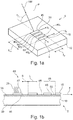
- Figure la-b illustrates an example of substrate 5.
- the substrate comprises a support 10 and a coating 15 covering the support.
- the substrate has a growth surface 20 intended to receive the growing nanotubes 25.
- the support comprises a silicon plate 30, of length, width and thickness respectively equal to 30 mm, 30 mm and 0.5 mm.
- the plate has a face totally covered with a thin layer of alumina, deposited by atomic layer deposition, (ALD), with a thickness of 10 nm.
- ALD atomic layer deposition
- the coating is in contact with the alumina layer. It is deposited by e-beam evaporation.
- the coating is a thin layer of iron, 1 nm thick. Iron is a catalyst for the growth of carbon nanotubes.
- the coating is in the form of strips 40 1-4 , each of a width L equal to 200 ⁇ m, arranged parallel to each other and periodically spaced in a direction X perpendicular to the directions Y 1-4 of band extensions, the separation distance S between the strips of the coating being equal to 500 ⁇ m.
- the coating comprises a first face 46 disposed opposite the support and a second face 47 opposite the first face, the second face defining a growth zone 45 for the mat of nanotubes.
- a portion (48) of the face of the support disposed between two strips of the coating defines a blank area 50 on the face of the substrate on which the coating is disposed.
- the virgin zone is devoid of catalyst and thus sterile to the growth of nanotubes.
- the growth zone and the blank zone thus define a measurement pattern 55 which is repeated periodically in the direction X, thus forming a measurement zone 60.
- the measurement zone has a rectangular contour of length L m and width l m equal to 15 mm and 10 mm.
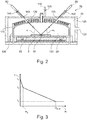
- the figure 2 illustrates an example of a device 70 for implementing the method according to the invention.
- the device comprises a chemical vapor deposition reactor 75, a laser diode 80 and a photodetector 85.
- the reactor comprises an enclosure 90 within which catalyzed growth of the nanotube mat takes place.
- the CVD deposition reactor is for example a “plate to plate” reactor sold by the company Plassys.
- the reactor includes a graphite heating substrate holder 95 housed in the enclosure, and on which the substrate 5 illustrated on the figure 1 .
- a quartz bell 100 overcomes the substrate holder and the substrate. It has an opening 105 for the entry of precursor gases from the nanotube material, illustrated by the arrow 110.
- the precursor gas includes acetylene, hydrogen and helium. Acetylene provides the carbon necessary for the growth of a carpet of carbon nanotubes.
- Heating elements 115 and thermal reflectors 120 are arranged between the wall 125 of the enclosure and the quartz bell to heat the reaction space 130 defined under the bell in which the catalysis reaction takes place.
- the enclosure further comprises an outlet opening 135 for the evacuation of gaseous reaction products.
- the nanotubes are grown by bringing the substrate holder to a temperature of 600 ° C.
- the pressure in the enclosure is 0.3 Torr.
- the laser diode is arranged outside the enclosure. It emits an incident light beam 140 in the form of a laser beam with a wavelength equal to 636 nm. It is oriented so that the laser beam is directed to irradiate the measurement area 55.
- the wall of the reactor enclosure further includes a quartz window 145 placed on the optical path of the incident laser beam.
- the angle of incidence ⁇ i of the laser on the measurement area is 42 °, defined between the direction of propagation of the laser and a normal not to the substrate.
- the growth zones and the virgin zones which each extend in a band along the directions Y 1-4 , parallel to one another, are arranged perpendicular to the plane P comprising the direction 150 of propagation of the incident laser beam.
- the incident laser beam is reflected by the measurement zone, as long as the nanotube mat has not reached a height such that it prevents the incident laser beam from reaching the virgin zones.
- the angle of reflection ⁇ r of the reflected laser beam is equal to the angle of incidence.
- the photodetector is disposed outside the enclosure along the optical path of the reflected beam 155.
- the wall of the enclosure further comprises a window 160 made of quartz to isolate the photodetector from the enclosure and transmit the reflected beam.
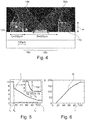
- the graph of the figure 3 schematically represents the evolution of the intensity I of the reflected beam as a function of the height H of the mat of nanotubes in the CVD reactor of the figure 2 .
- the measurement zone reflects the incident laser beam, as a function of the reflection properties of the thin layer of alumina defining the virgin zone and of the thin layer of iron defining the growth zone.
- An intensity I 1 is measured.
- the nanotubes are grown. During growth, no catalyst being present on the virgin areas, no nanotube grows on the latter. On the contrary, by interaction between the precursor gas comprising acetylene and iron, carbon nanotubes grow on the growth zones. In the example illustrated, the growth zones are reflective before the carbon nanotubes grow.
- the nanotube mat no longer reflects the incident laser beam as soon as it reaches the instant t 2 a height H 2 , which in the illustrated example is of the order of 4 ⁇ m, as can be verified a posteriori by means of a measurement on a photograph taken for example by scanning electron microscopy or a reflectivity measurement on a portion of the substrate free of "virgin" area.
- the intensity therefore decreases rapidly as a function of the height H between the start of the growth where the height is zero and the height H 2 .
- the mat of carbon nanotubes is semi-transparent and optical interference can be observed as shown on the curve illustrated on the figure 5 .
- the mat 170 of nanotubes absorbs part of the laser beam and, in this way, forms a shadow 180 on the blank area.
- the part 185 of the virgin zone irradiated by the incident laser beam and which is reflected then decreases linearly with increasing height. It is then worth S-2H / tan ( ⁇ ).
- the intensity of the reflected beam then also decreases linearly until it reaches a minimum threshold intensity I 3 , for which the nanotube mats which have grown on the growth zones form screens shading all the virgin zones. Substantially no beam is then reflected by the measurement area.
- the minimum threshold intensity I 3 therefore corresponds to the maximum height of the mat of nanotubes that can be measured. It can be non-zero and correspond to the intensity of parasitic radiation measured by the photodetector.
- Equation (2) provides a determination of the height H with an accuracy of the order of H 2/2.
- the intensities I 1 and I 3 expressed in output voltage measured on the photodiode are equal to 10 V and 0V.
- the evolution of the intensity I, expressed in volts, of the reflected beam as a function of the growth time t of the mat of nanotubes is illustrated on the figure 5 .
- Nanotubes grow between t 1 and t 2 ' .
- the intensity decreases quickly between instants t 1 and t 2 , time at which the mat reaches the height H 2 .
- the attenuation 190 of the intensity between the instants t 1 and t 2 respects equation (1).
- the intensity of the reflected beam decreases more weakly during the growth of the mat of nanotubes until time t 2 ' .
- the height H of the carbon nanotube mat can be determined with an accuracy of H 2/2 depending on the growth time t, as shown in figure 6 .
- a carpet height of 185 ⁇ 2 ⁇ m is measured in this example.
- the height H 2 is 4 ⁇ m for the example of implementation of the method.
- the method according to the invention is therefore particularly well suited to measuring the height of nanotube mats obtained in industrial reactors.
- the measurement area can be formed of a plurality of blank areas arranged so as to form a hexagonal network, the blank areas having a circular outline and being surrounded by a surrounding growth area.
Landscapes
- Chemical & Material Sciences (AREA)
- Engineering & Computer Science (AREA)
- Materials Engineering (AREA)
- Organic Chemistry (AREA)
- Nanotechnology (AREA)
- Inorganic Chemistry (AREA)
- Chemical Kinetics & Catalysis (AREA)
- General Chemical & Material Sciences (AREA)
- Mechanical Engineering (AREA)
- Metallurgy (AREA)
- General Physics & Mathematics (AREA)
- Physics & Mathematics (AREA)
- Carbon And Carbon Compounds (AREA)
- Length Measuring Devices By Optical Means (AREA)
- Investigating Or Analysing Materials By Optical Means (AREA)
Abstract
L'invention concerne un procédé de mesure de la hauteur (H) d'un tapis de nanotubes de carbone, comportant :a) la fourniture d'un substrat (5) présentant une surface de croissance (20) contenant au moins une zone de mesure (60) comportant une zone de croissance (45) et une zone stérile,la zone de croissance étant définie par une portion du substrat contenant un catalyseur de croissance des nanotubes, etb) la croissance catalytique par CVD du tapis (170) de nanotubes sur la zone de croissance,et au moins au cours de l'étape b) :- l'irradiation de la zone de mesure avec un faisceau lumineux incident (140) ;- la mesure en différents instants de l'intensité (I) du faisceau réfléchi (155) par la zone de mesure ;- la détermination de la hauteur du tapis de nanotubes à partir des intensités du faisceau réfléchi mesurées aux différents instants (t).
Description
- La présente invention concerne un procédé de mesure de la hauteur d'un tapis de nanotubes en croissance.
- La synthèse de tapis de nanotubes de carbone, est opérée industriellement par dépôt chimique en phase vapeur (dénommé « CVD » pour l'acronyme anglais de « Chemical Vapor Deposition »), sur un support recouvert d'un catalyseur de la croissance des nanotubes. Un tel procédé est particulièrement sensible aux nombreux paramètres de pilotage d'un réacteur de dépôt par CVD ainsi qu'aux conditions environnementales (température et humidité par exemple). Il est en particulier difficile à contrôler pour obtenir de manière reproductible une hauteur souhaitée du tapis de nanotubes, comme cela est par exemple décrit dans l'article C. Ryan Oliver et al., « Statistical analysis of variation in laboratory growth of carbon nanotubes forests and recommendations for improved consistency », ACS NANO, vol. 7, No. 4, pp 3565-3580, 2013.
- Or, pour certaines applications, par exemple lorsque le tapis de nanotubes est destiné à former un organe d'interposition pour la gestion thermique d'un composant électronique, ou à former un fil ou une nappe, il est nécessaire de produire un tapis avec une hauteur contrôlée.
- Des méthodes sont connues pour déterminer l'évolution de la hauteur d'un tapis de nanotubes en croissance.
- Par exemple, l'article A. A. Puretzky et al., « real-time imaging of vertically aligned carbon nanotube array growth kinetics », Nanotechnology, 19 (2008), p. 05560 décrit une méthode de suivi de la hauteur au moyen d'images prises à l'aide d'un téléobjectif. Une succession d'images de la section transversale d'un tapis de nanotubes en croissance située sur le bord d'un substrat est analysée. Toutefois, outre sa résolution limitée, une telle méthode est réservée au suivi de la croissance sur des substrats d'une taille inférieure aux substrats industriels. Il est en effet nécessaire que la croissance en périphérie du substrat soit sensiblement homogène à celle au centre du substrat. Une telle méthode ne peut donc pas être mise en œuvre industriellement.
- L'article E.R. Meshot et A.J. Hart, « Abrupt self-termination of vertically aligned carbon nanotube growth », Applied Physics Letters 92, 113107 (2008), propose de détecter la position d'une portion de la face supérieure d'un tapis de nanotubes en croissance au moyen d'un faisceau laser. Toutefois, en raison du caractère optiquement absorbant d'un tapis de nanotubes, cette technique requiert le dépôt d'un élément réfléchissant sur la portion, ce qui perturbe localement les échanges thermiques et gazeux, si bien que la hauteur du tapis de nanotubes sous la portion recouverte par le revêtement peut être sensiblement différente des autres portions du tapis.
- L'article Y. Hayashi et al., « Analysis of early stages of vertically aligned carbon nanotube growth by plasma-enhanced chemical vapor deposition », Japanese Journal of Applied Physics, vol. 44, No. 4A, 2005 pp. 1549-1553 et l'article D.B. Geoghegan et al., « In situ growth rate measurements and length control during chemical vapor deposition of vertically aligned multiwall carbon nanotubes », Applied Physics Letters, Vol. 83, No. 9, 2003, pp 1851-1853 décrivent le suivi de la hauteur de tapis de nanotubes en croissance par ellipsométrie et par réflectométrie respectivement. Les auteurs mettent à profit ces techniques pour déterminer la hauteur d'un tapis de nanotubes en quantifiant la modification de la polarisation et de l'intensité d'un faisceau lumineux respectivement, après réflexion par un tapis de nanotubes. Néanmoins, de telles techniques sont pénalisées par l'absorption optique du tapis de nanotubes. Elles sont inadaptées à la mesure de la hauteur de tapis présentant une hauteur supérieure à 10 µm. Or, les tapis de nanotubes produits industriellement présentent des hauteurs qui peuvent être supérieures à 100 µm.
- Il existe donc un besoin pour une méthode qui permette de mesurer, de manière fiable et reproductible, la hauteur d'un tapis de nanotubes dans des conditions industrielles de croissance.
- L'invention répond à ce besoin et propose un procédé de mesure de la hauteur d'un tapis de nanotubes de carbone, le procédé comportant les étapes de :
- a) fourniture d'un substrat présentant au moins une surface de croissance, la surface de croissance contenant au moins une zone de mesure comportant une zone de croissance et une zone stérile à la croissance des nanotubes, dite zone « vierge »,
la zone de croissance étant définie par une portion du substrat contenant un catalyseur de la croissance des nanotubes, et - b) croissance catalytique, au sein d'un réacteur de dépôt chimique en phase vapeur, du tapis de nanotubes sur la zone de croissance,
- l'irradiation de la zone de mesure au moyen d'un faisceau lumineux incident;
- la mesure en différents instants de l'intensité du faisceau réfléchi par la zone de mesure ;
- la détermination de la hauteur du tapis de nanotubes à partir des intensités du faisceau réfléchi mesurées aux différents instants (t).
- Une mesure simple de la hauteur du tapis de nanotubes de carbone peut être effectuée au moyen du procédé. En particulier, la mesure de la hauteur du tapis sur la zone de mesure est représentative de la hauteur du tapis pouvant croître en des zones différentes et notamment éloignées de la zone de mesure. Par ailleurs, la croissance des nanotubes sur des zones différentes de la zone de mesure n'est pas affectée par la présence de la zone de mesure. Notamment, le procédé peut être mis en œuvre sans qu'un élément soit déposé sur le tapis de nanotubes. On limite ainsi l'introduction d'artefacts expérimentaux dans la détermination de la hauteur.
- Par ailleurs, le procédé selon l'invention requiert peu, voire pas de modifications du réacteur de dépôt CVD.
- En outre, la zone de mesure peut être disposée sur une partie du substrat qui est destinée à être sacrifiée, par exemple découpée, une fois que la croissance du tapis de nanotubes est finie. Ainsi, le procédé ne réduit pas le rendement de production de tapis de nanotubes.
- Par ailleurs, le procédé permet la mesure de hauteurs de tapis de nanotubes produits industriellement. En particulier, comme cela sera apparent par la suite, en fonction de la forme et des dimensions de la zone de croissance et de la zone vierge, ainsi que de l'angle d'incidence du faisceau incident sur le substrat, des hauteurs supérieures à 150 µm, voire même supérieures à 500 µm peuvent être mesurées, mieux supérieures à 1 mm.
- De préférence, la zone vierge est définie par une autre portion du substrat qui absorbe moins et/ou réfléchit plus le faisceau lumineux incident que le tapis de nanotubes. On tire ainsi profit du caractère optiquement absorbant des nanotubes qui occultent progressivement au cours de la croissance du tapis, à la manière d'un diaphragme, l'intensité du faisceau réfléchi.
- L'homme du métier sait aisément déterminer de telles propriétés. Le coefficient d'absorption d'un tapis de nanotubes de carbone, mesuré par spectroscopie optique, peut être compris entre 0,95 et 0,9999 dans la gamme spectrale de longueurs d'ondes comprises entre 200 nm et 20 µm, par exemple supérieur à 0,97 à une longueur d'onde égale à 635 nm. Par exemple, le substrat peut comporter une zone vierge définie par de l'alumine sur du silicium qui présente un coefficient de réflexion supérieur à 15% à une longueur d'onde égale à 635 nm. Le coefficient de réflexion peut notamment être mesuré par réflectométrie.
- Un « tapis de nanotubes » désigne un assemblage organisé de nanotubes de carbone, dans lequel les nanotubes sont sensiblement parallèles les uns aux autres, orientés chacun sensiblement perpendiculairement à la surface de croissance sur laquelle ils ont crû, et dont la hauteur est proche de la longueur unitaire des nanotubes.
- Par « croissance catalytique » du tapis de nanotubes, on entend que la croissance des nanotubes du tapis est activée au moyen du catalyseur.
- A l'étape a), on dispose d'un substrat présentant une surface de croissance pour la croissance catalytique des nanotubes de carbone.
- L'homme du métier sait de manière routinière choisir un tel catalyseur.
- Le catalyseur peut notamment comporter un élément choisi parmi le fer, le cobalt, le nickel, le palladium et leurs mélanges.
- De préférence, le substrat comporte un support et un revêtement recouvrant partiellement le support. Un « support » présente une rigidité telle qu'il ne rompt pas sous l'effet de son propre poids.
- Un tel revêtement peut être déposé sur le support par différentes méthodes connues de l'homme du métier. Par exemple, il peut être déposé par évaporation e-beam.
- De préférence, le revêtement contient le catalyseur. Le revêtement peut être multicouche. Par exemple, il est constitué d'une couche d'aluminium d'épaisseur pouvant être comprise entre 1 nm et 100 nm et d'une couche formée du catalyseur. Il peut aussi être constitué de plusieurs couches métalliques, par exemple en titane et en aluminium, et d'une couche formée du catalyseur. Le brevet
WO-A-2014/191915 décrit un exemple d'un tel revêtement multicouche. - Le support peut être constitué par un bloc ou une plaque métallique, éventuellement recouvert d'un ou plusieurs oxydes, par exemple de l'alumine, ou d'un matériau carboné, par exemple du graphène ou du carbone amorphe, ou de métaux, par exemple de l'aluminium, du TaN ou du TiN. Le support peut être multicouche. Par exemple, il est constitué d'une plaque de silicium ayant notamment une épaisseur supérieure à 0,3 mm, recouverte d'une couche d'alumine d'épaisseur pouvant être comprise entre 1 nm et 100 nm.
- Le revêtement peut être formé sur le support, de manière à définir la zone de croissance et le cas échéant la zone vierge, par une méthode choisie par l'homme de l'art. Par exemple, le revêtement peut être déposé à travers un masque mécanique, au moyen d'un masquage résine, ou être obtenu par ablation après dépôt d'un revêtement ou de la couche catalytique.
- Le revêtement présente une première face en regard du support et une deuxième face opposée à la première face. De préférence, la zone de croissance est définie par la deuxième face.
- De préférence, la zone vierge est au moins partiellement définie par la portion de la face du support, dite « portion libre », complémentaire à la portion de la face du support recouverte par le revêtement. La zone vierge est de préférence définie par une portion du support, par exemple la portion libre, en un matériau inerte vis-à-vis de la croissance des nanotubes. L'homme du métier sait choisir simplement et de manière routine un tel matériau inerte.
- La zone de croissance et la zone vierge sont de préférence contigües. De préférence la zone vierge est séparée par deux zones de croissance consécutives.
- De préférence, la zone de croissance et la zone vierge définissent un motif de mesure, la zone de mesure étant définie par la répétition régulière, de préférence périodique, selon au moins une direction du motif de mesure. La zone de mesure peut être définie par la répétition régulière, de préférence périodique, selon deux directions orthogonales ou non.
- Le motif peut être répété au moins 1 fois, de préférence au moins 3 fois, voire au moins 10 fois selon au moins une direction de sorte que la zone de mesure soit d'étendue plus grande que la surface projetée du faisceau lumineux incident sur le substrat.
- Par exemple, le motif de mesure peut être répété selon deux directions orthogonales de telle sorte que les zones de croissance et zone vierge soient disposées dans la zone de mesure à la manière d'un damier.
- De préférence, la zone de croissance et la zone vierge présentent chacune une forme de bande, de préférence rectiligne. La zone de croissance et la zone vierge peuvent s'étendre selon des directions parallèles. Elles s'étendent de préférence selon une direction commune. En particulier, elles peuvent partager un bord long commun et définir le motif de mesure, qui de préférence est répété périodiquement le long d'une direction perpendiculaire à la direction d'extension commune.
- De préférence, la zone de croissance en bande présente une largeur comprise entre 30 µm et 500 µm, par exemple égale à 200 µm et/ou la zone vierge en bande présente une largeur comprise entre 30 et 10000 µm, par exemple égale à 500 µm.
- La zone de mesure peut présenter un contour de forme variée, par exemple rectangulaire, circulaire, carré ou losange.
- Elle peut être disposée dans la partie centrale de la surface de croissance ou auprès du bord du substrat.
- De préférence, l'aire de la zone de mesure est supérieure à la taille du faisceau lumineux sur le support.
- Par ailleurs, le substrat peut comporter une autre zone de croissance, définie par une autre portion du substrat comportant le catalyseur, et disposée à distance de la zone de mesure. L'autre zone de croissance encadre par exemple la zone de mesure. L'autre zone de croissance est ainsi destinée à la production industrielle d'un tapis de nanotubes ou de composants intégrants des tapis de nanotubes.
- La zone de mesure peut être disposée sur une partie du substrat destinée à être sacrifiée en fin d'étape de croissance du tapis de nanotubes. Par exemple, en fin de d'étape de croissance des nanotubes, l'autre zone de croissance peut être recouverte par un autre tapis de nanotubes, et le substrat peut être découpé selon un tracé de découpe incluant la zone de mesure.
- A l'étape b), on fait croître des nanotubes sur la zone de croissance.
- La croissance du tapis de nanotubes est opérée dans l'enceinte d'un réacteur de croissance catalytique par dépôt chimique en phase vapeur.
- La croissance par CVD des nanotubes peut être menée de manière conventionnelle dans le domaine considéré. L'homme du métier sait définir de manière routinière les paramètres, notamment la température, la pression et le débit des gaz précurseurs du matériau constitutif des nanotubes, permettant de garantir la croissance des nanotubes sur la surface de croissance d'un substrat disposé dans l'enceinte du réacteur CVD.
- Par exemple, pour faire croître un tapis de nanotubes de carbone, l'homme du métier peut choisir un précurseur carboné étant par exemple l'acétylène.
- Le substrat peut être porté dans l'enceinte à une température comprise entre 350 °C et 900 °C, en particulier comprise entre 500 °C et 700 °C.
- La pression de l'enceinte peut être comprise entre comprise entre 0,1 mbar et 1000 mbar, en particulier entre 0,1 et 10 mbar.
- Par ailleurs, au moins au cours de la croissance du tapis de nanotubes à l'étape b), on détermine la hauteur du tapis de nanotubes.
- La détermination de la hauteur du tapis de nanotubes requiert au préalable l'irradiation de la zone de mesure au moyen d'un faisceau lumineux incident, puis la mesure de l'intensité du faisceau réfléchi par la zone de mesure.
- Lorsqu'un précurseur des nanotubes entre en contact de la zone de croissance, une réaction catalysée par le catalyseur s'opère entre les précurseurs des nanotubes. Les nanotubes croissent alors selon une direction sensiblement perpendiculaire à la surface de croissance du substrat.
- Au contraire, au contact de la zone vierge, sensiblement aucune réaction ne s'opère du fait d'une absence du catalyseur. Sensiblement aucun nanotube ne croît à partir de la zone vierge. Ainsi, au cours de la croissance, la zone vierge reste sensiblement exempte de nanotubes. Par ailleurs, les propriétés optiques du matériau de la partie du substrat qui définit la zone vierge restent de préférence constantes au cours de la croissance des nanotubes.
- Le faisceau lumineux incident peut être monochromatique ou polychromatique. En particulier, le faisceau lumineux incident peut être un faisceau laser parallèle, de préférence ayant une longueur d'onde comprise entre 200 nm et 20 µm, voire entre 350 nm et 700 nm, par exemple égale à 635 nm. En particulier, le faisceau lumineux incident peut présenter un diamètre compris entre 1 µm et 1 cm.
- En variante, le faisceau lumineux incident peut être un faisceau de lumière visible, notamment polychromatique et présentant un spectre de longueurs d'ondes comprises entre 200 nm et 800 nm, voire comprises entre 380 nm et 780 nm.
- Le faisceau lumineux incident peut être émis par une source lumineuse, par exemple une diode laser, reliée à une source d'alimentation électrique. L'intensité du faisceau lumineux incident peut ainsi aisément déterminable, si nécessaire.
- La zone de mesure peut être irradiée pendant au moins 50 % de la durée de l'étape b) de croissance ou tout au long de la croissance du tapis de nanotubes.
- La source lumineuse est de préférence disposée à l'extérieur de l'enceinte du réacteur catalytique. La ou les parois séparant l'enceinte de la source lumineuse peuvent comporter une ouverture et/ou une portion transparente au faisceau lumineux incident, par exemple un hublot en quartz, pour la transmission du faisceau lumineux incident de la source vers le substrat. La source lumineuse est ainsi protégée de l'atmosphère et des effets de la température pouvant régner dans l'enceinte au cours du dépôt.
- La hauteur maximale d'un tapis de nanotubes pouvant être déterminée peut être liée à la valeur de l'angle d'incidence du faisceau lumineux incident. L'angle d'incidence est défini entre la direction du faisceau lumineux et la surface de croissance.
- L'angle d'incidence du faisceau lumineux incident peut être supérieur à 0 °, de préférence supérieur à 10 ° et/ou inférieur à 90 °, par exemple inférieur à 80 °, de préférence compris entre 30 ° et 60 °. Ainsi, au fur et à mesure de sa croissance, le tapis de nanotubes définit un écran qui empêche le rayonnement incident d'atteindre une partie de la zone vierge, dite « partie ombrée ».
- Par ailleurs, dans la variante où la zone de croissance et la zone vierge se présentent chacune sous la forme d'une bande, de préférence les zone de croissance et zone vierge sont de préférence perpendiculaires au plan normal au substrat comportant la direction de propagation du faisceau lumineux incident. Une telle disposition de la zone de mesure par rapport au faisceau lumineux incident facilite la détermination de la hauteur du tapis de nanotubes.
- De préférence, le faisceau lumineux incident irradie au moins 50 % et de préférence moins de 90 % de l'aire de la zone de mesure.
- Le faisceau incident est réfléchi par la zone de mesure.
- L'intensité du faisceau réfléchi peut être mesurée au moyen d'un photodétecteur. Le photodétecteur est de préférence disposé hors de l'enceinte, afin de le protéger des gaz réactifs et de la température de l'enceinte. La ou les parois séparant l'enceinte du photodétecteur peuvent comporter une ouverture et/ou une autre portion transparente au faisceau réfléchi pour transmettre le faisceau réfléchi de la zone de mesure au photodétecteur.
- Le photodétecteur comporte par exemple une photodiode en silicium. Il peut comporter un filtre passe-bande centré sur la ou les longueurs d'onde du faisceau incident, qui peut être monté sur la photodiode, pour réduire l'influence de la lumière environnante. Par ailleurs, un miroir chaud peut être monté sur la photodiode, pour limiter l'influence du rayonnement infrarouge pouvant être émis par l'enceinte et les objets qui y sont contenus, sur la mesure de l'intensité du rayonnement réfléchi.
- La mesure de l'intensité du faisceau réfléchi est de préférence effectuée en continu tout au long de la croissance du tapis de nanotubes.
- Par exemple, l'intensité du faisceau lumineux peut être mesurée avec une fréquence de mesure comprise entre 0,1 Hz et 1 MHz.
- L'intensité du faisceau réfléchi peut décroître avec une augmentation de la hauteur du tapis de nanotubes. Elle peut notamment décroître plus rapidement dans une première phase de croissance que dans une deuxième phase successive à la première phase.
- En particulier, l'intensité du faisceau réfléchi peut décroître par morceaux en fonction de la hauteur du tapis de nanotubes. De préférence, elle décroît par morceaux selon des première et deuxième portions. La première portion présente des oscillations atténuées, qui résultent d'interférences optiques que l'homme de l'art sait reconnaître et exploiter, par exemple au moyen d'une technique de réflectométrie classique. La deuxième portion décroît linéairement avec la hauteur du tapis de nanotubes.
- En particulier, l'intensité du faisceau réfléchi peut décroître en fonction de la hauteur du tapis de nanotubes, jusqu'à atteindre une intensité seuil minimale. De préférence, la hauteur maximale mesurable du tapis de nanotubes est déterminée au premier instant de mesure où l'intensité du faisceau réfléchi atteint l'intensité seuil minimale. L'intensité seuil minimale peut être nulle ou résulter des effets de la lumière parasite atteignant le photodétecteur.
- La hauteur du tapis de nanotubes est déterminée à partir des intensités du faisceau réfléchi mesurées aux différents instants. En particulier, l'intensité du faisceau réfléchi est mesurée en au moins deux instants différents de la croissance.
- De préférence, pendant au moins une partie de la croissance du tapis de nanotubes, la hauteur du tapis de nanotubes croît, de préférence de façon continûment monotone, en fonction de la décroissance de l'intensité du faisceau réfléchi. De préférence, pendant au moins une partie de la croissance du tapis de nanotubes, la hauteur du tapis de nanotubes croît de préférence de façon continûment monotone et linéairement en fonction de la décroissance de l'intensité du faisceau réfléchi.
- L'invention pourra être mieux comprise à la lecture de la description détaillée qui va suivre et du dessin annexé dans lequel :
- les
figures 1a et 1b illustrent un substrat, vu en perspective et en coupe respectivement, pour la mise en œuvre du procédé selon l'invention, - la
figure 2 illustre un dispositif pour la mise en œuvre du procédé selon l'invention, 1 - la
figure 3 est un graphique représentant schématiquement l'évolution de l'intensité du faisceau réfléchi en fonction de la hauteur du tapis de nanotubes, - la
figure 4 est une photographie prise en microscopie à balayage d'une section transverse du substrat sur lequel a crû un tapis de nanotubes selon un exemple de mise en œuvre du procédé, - la
figure 5 est un graphique représentant l'évolution au cours d'un exemple de mise en œuvre du procédé, l'évolution de l'intensité du faisceau réfléchi, et - la
figure 6 est un graphique représentant l'évolution de la hauteur du tapis de nanotubes en fonction de la durée de croissance. - Les éléments représentés sur le dessin le sont en échelle libre.
- La figure la-b illustre un exemple de substrat 5.
- Le substrat comporte un support 10 et un revêtement 15 recouvrant le support. Le substrat présente une surface de croissance 20 destiné à recevoir les nanotubes 25 en croissance.
- Le support comporte une plaque 30 de silicium, de longueur, largeur et épaisseur respectivement égales à 30 mm, 30 mm et 0,5 mm. La plaque présente une face totalement recouverte d'une couche mince 35 d'alumine, déposée par dépôt de couche atomique, (ALD), d'une épaisseur de 10 nm. Le revêtement est au contact de la couche d'alumine. Il est déposé par évaporation e-beam.
- Le revêtement est une couche mince de fer, d'une épaisseur de 1 nm. Le fer est un catalyseur de la croissance de nanotubes de carbone.
- Le revêtement se présente sous la forme de bandes 401-4, chacune d'une largeur L égale à 200 µm, disposées parallèlement les unes aux autres et espacées périodiquement selon une direction X perpendiculaire aux directions Y1-4 d'extensions des bandes, la distance de séparation S entre les bandes du revêtement étant égale à 500 µm.
- Le revêtement comporte une première face 46 disposée en regard du support et une deuxième face 47 opposée à la première face, la deuxième face définissant une zone de croissance 45 pour le tapis de nanotubes. Une portion (48) de la face du support disposée entre deux bandes du revêtement définit quant à elle une zone vierge 50 sur la face du substrat sur laquelle le revêtement est disposé. La zone vierge est exempte de catalyseur et ainsi stérile à la croissance des nanotubes.
- La zone de croissance et la zone vierge définissent ainsi un motif de mesure 55 qui est répété périodiquement selon la direction X, formant ainsi une zone de mesure 60. La zone de mesure présente un contour rectangulaire de longueur Lm et largeur lm égales à 15 mm et 10 mm.
- La
figure 2 illustre un exemple de dispositif 70 pour mettre en œuvre le procédé selon l'invention. - Le dispositif comporte un réacteur 75 de dépôt chimique en phase vapeur, une diode 80 laser et un photodétecteur 85.
- Le réacteur comporte une enceinte 90 au sein de laquelle s'opère la croissance catalysée du tapis de nanotubes. Le réacteur de dépôt CVD est par exemple un réacteur « plaque à plaque » commercialisé par la société Plassys.
- Le réacteur comporte un porte-substrat 95 chauffant en graphite logé dans l'enceinte, et sur lequel est disposé le substrat 5 illustré sur la
figure 1 . - Une cloche 100 en quartz surmonte le porte substrat et le substrat. Elle est dotée d'une ouverture 105 pour l'entrée de gaz précurseurs du matériau des nanotubes, illustrée par la flèche 110. Dans l'exemple de la
figure 2 , le gaz précurseur comporte de l'acétylène, de l'hydrogène et de l'hélium. L'acétylène apporte le carbone nécessaire à la croissance d'un tapis de nanotubes de carbone. - Des éléments chauffants 115 et des réflecteurs thermiques 120 sont disposés entre la paroi 125 de l'enceinte et la cloche en quartz pour chauffer l'espace de réaction 130 défini sous la cloche dans lequel se produit la réaction de catalyse.
- L'enceinte comporte en outre une ouverture de sortie 135 pour l'évacuation des produits de réaction gazeux.
- Dans l'exemple de la
figure 2 , la croissance des nanotubes est opérée en portant le porte substrat à une température de 600°C. La pression dans l'enceinte est de 0,3 Torr. - La diode laser est disposée à l'extérieur de l'enceinte. Elle émet un faisceau lumineux incident 140 sous forme d'un faisceau laser d'une longueur d'onde égale à 636 nm. Elle est orientée de sorte que le faisceau laser soit dirigé pour irradier la zone de mesure 55. A cette fin, la paroi de l'enceinte du réacteur comporte en outre un hublot 145 en quartz disposé sur le chemin optique du faisceau laser incident.
- L'angle d'incidence αi du laser sur la zone de mesure est de 42 °, défini entre la direction de propagation du laser et une normale
n au substrat. Comme cela est représenté sur lafigure 1 , les zones de croissance et les zones vierges, qui s'étendent chacune en bande selon les directions Y1-4, parallèles les unes autres, sont disposées perpendiculairement au plan P comportant la direction 150 de propagation du faisceau laser incident. - Le faisceau laser incident est réfléchi par la zone de mesure, tant que le tapis de nanotubes n'a pas atteint une hauteur telle qu'il empêche le faisceau laser incident d'atteindre les zones vierges.
- L'angle de réflexion αr du faisceau laser réfléchi est égal à l'angle d'incidence.
- Le photodétecteur est disposé hors de l'enceinte le long du trajet optique du faisceau réfléchi 155. La paroi de l'enceinte comporte en outre une fenêtre 160 en quartz pour isoler le photodétecteur de l'enceinte et transmettre le faisceau réfléchi.
- Le graphique de la
figure 3 représente schématiquement l'évolution de l'intensité I du faisceau réfléchi en fonction de la hauteur H du tapis de nanotubes dans le réacteur CVD de lafigure 2 . - Avant que la croissance des nanotubes ne soit opérée, la zone de mesure réfléchit le faisceau laser incident, en fonction des propriétés de réflexion de la couche mince d'alumine définissant la zone vierge et de la couche mince de fer définissant la zone de croissance. Une intensité I1 est mesurée.
- A partir de t=t1, on opère la croissance des nanotubes. Au cours de la croissance, aucun catalyseur n'étant présent sur les zones vierges, aucun nanotube ne croît sur ces dernières. Au contraire, par interaction entre le gaz précurseur comportant l'acétylène et le fer, des nanotubes de carbone croissent sur les zones de croissance. Dans l'exemple illustré, les zones de croissance sont réfléchissantes avant que ne croissent les nanotubes de carbone. Le tapis de nanotubes ne réfléchit plus le faisceau laser incident dès qu'il atteint à l'instant t2 une hauteur H2, qui dans l'exemple illustré est de l'ordre de 4 µm, comme cela peut être vérifié a posteriori au moyen d'une mesure sur une photographie prise par exemple en microscopie électronique à balayage ou d'une mesure de réflectivité sur une portion du substrat exempte de zone « vierge ». L'intensité décroît donc rapidement en fonction de la hauteur H entre le début de la croissance où la hauteur est nulle et la hauteur H2. Tant que la hauteur est inférieure à H2, le tapis de nanotubes de carbone est semi-transparent et on peut observer des interférences optiques comme cela se manifeste sur la courbe illustrée sur la
figure 5 . - Lorsque la hauteur H augmente, comme cela est illustré sur la
figure 4 , le tapis 170 de nanotubes absorbe une partie du faisceau laser et, de cette façon, forme une ombre 180 sur la zone vierge. La partie 185 de la zone vierge irradiée par le faisceau laser incident et qui est réfléchi diminue alors linéairement avec l'augmentation de la hauteur. Elle vaut alors S-2H/tan(α). L'intensité du faisceau réfléchi diminue alors aussi linéairement jusqu'à atteindre une intensité seuil minimale I3, pour laquelle les tapis de nanotube ayant crû sur les zones de croissance forment des écrans ombrant toutes les zones vierges. Sensiblement aucun faisceau n'est alors réfléchi par la zone de mesure. L'intensité seuil minimale I3 correspond donc à la hauteur maximale du tapis de nanotubes pouvant être mesurée. Elle peut être non nulle et correspondre à l'intensité des rayonnements parasites mesurés par le photodétecteur. - Dans l'exemple illustré, l'intensité I2 vérifie l'équation (1) suivante :

- Lorsque l'intensité du faisceau réfléchi est comprise entre I2 et I3, la hauteur du tapis H peut être déterminée, de manière approchée, en résolvant l'équation (2)

- L'équation (2) fournit une détermination de la hauteur H avec une précision de mesure de l'ordre de H2/2.
- Par exemple dans l'exemple illustré, les intensités I1 et I3 exprimées en tension de sortie mesurée sur la photodiode sont égales à 10 V et 0V.
- L'évolution de l'intensité I, exprimée en volts, du faisceau réfléchi en fonction de la durée de croissance t du tapis de nanotubes est illustrée sur la
figure 5 . La croissance des nanotubes est opérée entre t1 et t2'. Comme expliqué ci-dessus l'intensité diminue rapidement entre les instants t1 et t2, instant auquel le tapis atteint la hauteur H2. L'atténuation 190 de l'intensité entre les instants t1 et t2 respecte l'équation (1). Par la suite, l'intensité du faisceau réfléchi décroit plus faiblement au cours de la croissance du tapis de nanotubes jusqu'à l'instant t2'. - Au moyen de l'équation 2, la hauteur H du tapis de nanotubes de carbone peut être déterminée avec une précision de H2/2 en fonction de la durée de croissance t, comme illustré sur la
figure 6 . Une hauteur de tapis atteignant 185 ± 2 µm est mesurée dans cet exemple. La hauteur H2 est de 4 µm pour l'exemple de mise en œuvre du procédé. - Le procédé selon l'invention est donc particulièrement bien adapté à la mesure de hauteur de tapis de nanotubes obtenus au sein de réacteurs industriels.
- L'invention n'est pas limitée aux exemples de mise en œuvre décrits ici à des fins illustratives.
- Notamment, d'autres motifs de mesure de forme plus complexe peuvent être envisagés. L'homme du métier sait alors adapter aisément les équations (1) et (2) en conséquence.
- Par exemple, pour faciliter le positionnement de la zone de mesure par rapport au faisceau incident, la zone de mesure peut être formée d'une pluralité de zones vierges disposées de manière à former un réseau hexagonal, les zones vierges présentant un contour circulaire et étant entourés par une zone de croissance environnante.
Claims (14)
- Procédé de mesure de la hauteur (H) d'un tapis de nanotubes de carbone, le procédé comportant les étapes de :a) fourniture d'un substrat (5) présentant une surface de croissance (20),
la surface de croissance contenant au moins une zone de mesure (60) comportant une zone de croissance (45) et une zone stérile à la croissance des nanotubes, dite zone « vierge » (50),
la zone de croissance étant définie par une portion du substrat contenant un catalyseur de la croissance des nanotubes, etb) croissance catalytique, au sein d'un réacteur (75) de dépôt chimique en phase vapeur, du tapis (170) de nanotubes sur la zone de croissance,le procédé comportant au moins au cours de l'étape b) :- l'irradiation de la zone de mesure au moyen d'un faisceau lumineux incident (140);- la mesure en différents instants de l'intensité (I) du faisceau réfléchi (155) par la zone de mesure ;- la détermination de la hauteur du tapis de nanotubes à partir des intensités du faisceau réfléchi mesurées aux différents instants (t). - Procédé selon la revendication 1, dans lequel la zone vierge est définie par une autre portion du substrat qui absorbe moins et/ou réfléchit plus le faisceau lumineux incident que le tapis de nanotubes.
- Procédé selon l'une quelconque des revendications 1 et 2, le substrat comportant un support (10) et un revêtement (15) recouvrant partiellement le support, le revêtement contenant le catalyseur.
- Procédé selon la revendication précédente, le revêtement comportant une première face (46) disposée en regard du support et une deuxième face (47) opposée à la première face, la zone de croissance étant définie par la deuxième face.
- Procédé selon l'une quelconque des revendications précédentes, dans lequel la zone vierge est définie par une portion du support en un matériau inerte vis-à-vis de la croissance des nanotubes.
- Procédé selon l'une quelconque des revendications précédentes, la zone vierge étant au moins partiellement définie par la portion (48) de la face du support complémentaire à la portion de la face du support recouverte par le revêtement.
- Procédé selon l'une quelconque des revendications précédentes, dans lequel la zone de croissance et la zone vierge définissent un motif de mesure (55), la zone de mesure étant définie par la répétition régulière, de préférence périodique, selon au moins une direction (X) du motif de mesure.
- Procédé selon l'une quelconque des revendications précédentes, la zone de croissance et la zone vierge présentant chacune une forme de bande, de préférence rectiligne.
- Procédé selon l'une quelconque des revendications précédentes, la zone de croissance présentant une largeur (L) comprise entre 30 µm et 500 µm, par exemple égale à 200 µm et/ou la zone vierge présentant une largeur (S) comprise entre 30 µm et 10000 µm, par exemple égale à 500 µm.
- Procédé selon l'une quelconque des revendications précédentes, dans lequel les zone de croissance et zone vierge sont perpendiculaires au plan comportant la direction de propagation du faisceau lumineux incident.
- Procédé selon l'une quelconque des revendications précédentes, dans lequel le faisceau lumineux incident est un faisceau laser parallèle, de préférence ayant une longueur d'onde comprise entre 200 nm et 20 µm, voire entre 350 nm et 700 nm, par exemple égale à 635 nm.
- Procédé selon l'une quelconque des revendications précédentes, dans lequel l'angle d'incidence (αi) du faisceau lumineux incident est supérieur à 0 °, de préférence est compris entre 30 ° et 60 °.
- Procédé selon l'une quelconque des revendications précédentes, dans lequel pendant au moins une partie de la croissance du tapis de nanotubes, la hauteur du tapis de nanotubes croît, de préférence de façon continûment monotone, en fonction de la décroissance de l'intensité du faisceau réfléchi.
- Procédé selon la revendication précédente, dans lequel pendant au moins une partie de la croissance du tapis de nanotubes, la hauteur du tapis de nanotubes croît de préférence de façon continûment monotone linéairement en fonction de de la décroissance de l'intensité du faisceau réfléchi.
Applications Claiming Priority (1)
| Application Number | Priority Date | Filing Date | Title |
|---|---|---|---|
| FR1858983A FR3086654B1 (fr) | 2018-09-28 | 2018-09-28 | Procede de mesure de la hauteur d'un tapis de nanotubes de carbone |
Publications (1)
| Publication Number | Publication Date |
|---|---|
| EP3632844A1 true EP3632844A1 (fr) | 2020-04-08 |
Family
ID=65685530
Family Applications (1)
| Application Number | Title | Priority Date | Filing Date |
|---|---|---|---|
| EP19200155.0A Withdrawn EP3632844A1 (fr) | 2018-09-28 | 2019-09-27 | Procede de mesure de la hauteur d'un tapis de nanotubes de carbone |
Country Status (3)
| Country | Link |
|---|---|
| US (1) | US20200103221A1 (fr) |
| EP (1) | EP3632844A1 (fr) |
| FR (1) | FR3086654B1 (fr) |
Citations (1)
| Publication number | Priority date | Publication date | Assignee | Title |
|---|---|---|---|---|
| WO2014191915A1 (fr) | 2013-05-28 | 2014-12-04 | Commissariat A L'energie Atomique Et Aux Energies Alternatives | Substrat conducteur electrique sur au moins une de ses faces muni d'un empilement de couches minces pour la croissance de nanotubes de carbone (ntc) |
-
2018
- 2018-09-28 FR FR1858983A patent/FR3086654B1/fr not_active Expired - Fee Related
-
2019
- 2019-09-26 US US16/583,309 patent/US20200103221A1/en not_active Abandoned
- 2019-09-27 EP EP19200155.0A patent/EP3632844A1/fr not_active Withdrawn
Patent Citations (1)
| Publication number | Priority date | Publication date | Assignee | Title |
|---|---|---|---|---|
| WO2014191915A1 (fr) | 2013-05-28 | 2014-12-04 | Commissariat A L'energie Atomique Et Aux Energies Alternatives | Substrat conducteur electrique sur au moins une de ses faces muni d'un empilement de couches minces pour la croissance de nanotubes de carbone (ntc) |
Non-Patent Citations (10)
| Title |
|---|
| A. A. PURETZKY ET AL.: "real-time imaging of vertically aligned carbon nanotube array growth kinetics", NANOTECHNOLOGY, vol. 19, 2008, pages 05560 |
| C. RYAN OLIVER ET AL.: "Statistical analysis of variation in laboratory growth of carbon nanotubes forests and recommendations for improved consistency", ACS NANO, vol. 7, no. 4, 2013, pages 3565 - 3580 |
| D.B. GEOGHEGAN ET AL.: "In situ growth rate measurements and length control during chemical vapor déposition of vertically aligned multiwall carbon nanotubes", APPLIED PHYSICS LETTERS, vol. 83, no. 9, 2003, pages 1851 - 1853 |
| E.R. MESHOTA.J. HART: "Abrupt self-termination of vertically aligned carbon nanotube growth", APPLIED PHYSICS LETTERS, vol. 92, 2008, pages 113107, XP012106053, doi:10.1063/1.2889497 |
| GEOHEGAN D B ET AL: "In situ growth rate measurements and length control during chemical vapor deposition of vertically aligned multiwall carbon nanotubes", APPLIED PHYSICS LETTERS, A I P PUBLISHING LLC, US, vol. 83, no. 9, 1 September 2003 (2003-09-01), pages 1851 - 1853, XP012035972, ISSN: 0003-6951, DOI: 10.1063/1.1605793 * |
| JÖNSSON M ET AL: "In situ growth rate measurements during plasma-enhanced chemical vapour deposition of vertically aligned multiwall carbon nanotube films", NANOTECHNOLOGY, IOP, BRISTOL, GB, vol. 18, no. 30, 1 August 2007 (2007-08-01), pages 305702, XP020119411, ISSN: 0957-4484, DOI: 10.1088/0957-4484/18/30/305702 * |
| KIM D-H ET AL: "In situ monitoring of carbon nanotube growth", CAR, ELSEVIER, OXFORD, GB, vol. 41, no. 3, 1 January 2003 (2003-01-01), pages 583 - 585, XP004408937, ISSN: 0008-6223, DOI: 10.1016/S0008-6223(02)00350-0 * |
| KIM, JANG, KIM, CHO, KANG, LEE: "Growth characterization of carbon nanotubes by using optical interference oscillations phenomena", vol. 41, no. 5, 30 November 2002 (2002-11-30), pages L587 - L590, XP002792909, Retrieved from the Internet <URL:http://citenpl.internal.epo.org/wf/web/citenpl/citenpl.html> [retrieved on 20190712] * |
| NG H T ET AL: "Growth of carbon nanotubes: a combinatorial method to study the effects of catalysts and underlayers", JOURNAL OF PHYSICAL CHEMISTRY. B, MATERIALS, SURFACES, INTERFACES AND BIOPHYSICAL, WASHINGTON, DC, US, vol. 107, no. 33, 21 August 2003 (2003-08-21), pages 8484 - 8489, XP002450951, ISSN: 1089-5647 * |
| Y. HAYASHI ET AL.: "Analysis of early stages of vertically aligned carbon nanotube growth by plasma-enhanced chemical vapor déposition", JAPANESE JOURNAL OF APPLIED PHYSICS, vol. 44, no. 4A, 2005, pages 1549 - 1553 |
Also Published As
| Publication number | Publication date |
|---|---|
| FR3086654B1 (fr) | 2020-10-30 |
| US20200103221A1 (en) | 2020-04-02 |
| FR3086654A1 (fr) | 2020-04-03 |
Similar Documents
| Publication | Publication Date | Title |
|---|---|---|
| EP2616855B1 (fr) | Filtre spectral passe bande à forte sélectivité et polarisation contrôlée | |
| EP2930506B1 (fr) | Dispositif de detection a resonateur acoustique differentiel de type helmholtz | |
| US9443715B2 (en) | Method and device for measuring temperature of substrate in vacuum processing apparatus | |
| CN102484085A (zh) | 利用光学吸收边波长测量薄膜的温度 | |
| TWI751412B (zh) | 內聯式腔室計量術 | |
| CN204945048U (zh) | 拉曼原位监控装置 | |
| FR2999803A1 (fr) | Dispositif de detection infrarouge | |
| GB2433737A (en) | A CVD single crystal diamond material | |
| FR2963101A1 (fr) | Detecteur de particules et procede de realisation d'un tel detecteur | |
| Sulaiman et al. | Synthesis and study of ZnO thin films using CVD technique for waveguide sensor applications | |
| EP4314773B1 (fr) | Surveillance de puits d'empreintes digitales chimiques 4d | |
| Amin-Chalhoub et al. | Chemical vapor deposition of low reflective cobalt (II) oxide films | |
| FR3062216A1 (fr) | Composant pour limiter l'angle d'incidence de la lumiere et procede pour realiser un tel composant ainsi que microspectrometre equipe d'un tel composant | |
| FR3086654A1 (fr) | Procede de mesure de la hauteur d'un tapis de nanotubes de carbone | |
| EP2368099B1 (fr) | Dispositif de spectroscopie optique comportant une pluralité de sources d'émission | |
| JP5090683B2 (ja) | 絶縁薄膜上にナノ構造体を含むヘイズノイズ標準の製造方法 | |
| Abb et al. | Ultrafast dephasing of light in strongly scattering gap nanowires | |
| FR2961913A1 (fr) | Filtre spectral avec membrane structuree a l'echelle sub-longueur d'onde et methode de fabrication d'un tel filtre | |
| FR3002687A1 (fr) | Procede de traitement d une structure | |
| Haugan et al. | Colloidal crystals as templates for light harvesting structures in solar cells | |
| EP3835756B1 (fr) | Dispositif et méthode de détection de particules et procédé de fabrication | |
| EP4537959B1 (fr) | Dispositif de détection d'un défaut au cours de la fabrication additive d'une pièce | |
| Enns et al. | Influence of Dewetting Conditions on the Optical Parameters of the AuNP/GaN Nanostructure | |
| EP2693271A1 (fr) | Appareil et procédé de mesure des dimensions de nanostructure 1-dimensionnelle et 0-dimensionnelle en temps réel pendant la croissance épitaxiale | |
| Evans | Growth, Optical Properties and Applications of Thin Film Diamond |
Legal Events
| Date | Code | Title | Description |
|---|---|---|---|
| PUAI | Public reference made under article 153(3) epc to a published international application that has entered the european phase |
Free format text: ORIGINAL CODE: 0009012 |
|
| STAA | Information on the status of an ep patent application or granted ep patent |
Free format text: STATUS: REQUEST FOR EXAMINATION WAS MADE |
|
| 17P | Request for examination filed |
Effective date: 20190927 |
|
| AK | Designated contracting states |
Kind code of ref document: A1 Designated state(s): AL AT BE BG CH CY CZ DE DK EE ES FI FR GB GR HR HU IE IS IT LI LT LU LV MC MK MT NL NO PL PT RO RS SE SI SK SM TR |
|
| AX | Request for extension of the european patent |
Extension state: BA ME |
|
| STAA | Information on the status of an ep patent application or granted ep patent |
Free format text: STATUS: THE APPLICATION IS DEEMED TO BE WITHDRAWN |
|
| 18D | Application deemed to be withdrawn |
Effective date: 20230401 |