EP3629367A1 - Substrate module, and method for producing substrate module - Google Patents
Substrate module, and method for producing substrate module Download PDFInfo
- Publication number
- EP3629367A1 EP3629367A1 EP18828625.6A EP18828625A EP3629367A1 EP 3629367 A1 EP3629367 A1 EP 3629367A1 EP 18828625 A EP18828625 A EP 18828625A EP 3629367 A1 EP3629367 A1 EP 3629367A1
- Authority
- EP
- European Patent Office
- Prior art keywords
- pads
- substrate
- spacers
- semiconductor chip
- chip
- Prior art date
- Legal status (The legal status is an assumption and is not a legal conclusion. Google has not performed a legal analysis and makes no representation as to the accuracy of the status listed.)
- Withdrawn
Links
Images



Classifications
-
- H—ELECTRICITY
- H05—ELECTRIC TECHNIQUES NOT OTHERWISE PROVIDED FOR
- H05K—PRINTED CIRCUITS; CASINGS OR CONSTRUCTIONAL DETAILS OF ELECTRIC APPARATUS; MANUFACTURE OF ASSEMBLAGES OF ELECTRICAL COMPONENTS
- H05K1/00—Printed circuits
- H05K1/02—Details
- H05K1/11—Printed elements for providing electric connections to or between printed circuits
- H05K1/111—Pads for surface mounting, e.g. lay-out
-
- H—ELECTRICITY
- H10—SEMICONDUCTOR DEVICES; ELECTRIC SOLID-STATE DEVICES NOT OTHERWISE PROVIDED FOR
- H10W—GENERIC PACKAGES, INTERCONNECTIONS, CONNECTORS OR OTHER CONSTRUCTIONAL DETAILS OF DEVICES COVERED BY CLASS H10
- H10W44/00—Electrical arrangements for controlling or matching impedance
- H10W44/20—Electrical arrangements for controlling or matching impedance at high-frequency [HF] or radio frequency [RF]
-
- H—ELECTRICITY
- H01—ELECTRIC ELEMENTS
- H01Q—ANTENNAS, i.e. RADIO AERIALS
- H01Q1/00—Details of, or arrangements associated with, antennas
- H01Q1/12—Supports; Mounting means
-
- H—ELECTRICITY
- H05—ELECTRIC TECHNIQUES NOT OTHERWISE PROVIDED FOR
- H05K—PRINTED CIRCUITS; CASINGS OR CONSTRUCTIONAL DETAILS OF ELECTRIC APPARATUS; MANUFACTURE OF ASSEMBLAGES OF ELECTRICAL COMPONENTS
- H05K1/00—Printed circuits
- H05K1/02—Details
- H05K1/14—Structural association of two or more printed circuits
-
- H—ELECTRICITY
- H05—ELECTRIC TECHNIQUES NOT OTHERWISE PROVIDED FOR
- H05K—PRINTED CIRCUITS; CASINGS OR CONSTRUCTIONAL DETAILS OF ELECTRIC APPARATUS; MANUFACTURE OF ASSEMBLAGES OF ELECTRICAL COMPONENTS
- H05K1/00—Printed circuits
- H05K1/02—Details
- H05K1/14—Structural association of two or more printed circuits
- H05K1/144—Stacked arrangements of planar printed circuit boards
-
- H—ELECTRICITY
- H05—ELECTRIC TECHNIQUES NOT OTHERWISE PROVIDED FOR
- H05K—PRINTED CIRCUITS; CASINGS OR CONSTRUCTIONAL DETAILS OF ELECTRIC APPARATUS; MANUFACTURE OF ASSEMBLAGES OF ELECTRICAL COMPONENTS
- H05K3/00—Apparatus or processes for manufacturing printed circuits
- H05K3/30—Assembling printed circuits with electric components, e.g. with resistors
- H05K3/32—Assembling printed circuits with electric components, e.g. with resistors electrically connecting electric components or wires to printed circuits
-
- H—ELECTRICITY
- H05—ELECTRIC TECHNIQUES NOT OTHERWISE PROVIDED FOR
- H05K—PRINTED CIRCUITS; CASINGS OR CONSTRUCTIONAL DETAILS OF ELECTRIC APPARATUS; MANUFACTURE OF ASSEMBLAGES OF ELECTRICAL COMPONENTS
- H05K3/00—Apparatus or processes for manufacturing printed circuits
- H05K3/40—Forming printed elements for providing electric connections to or between printed circuits
- H05K3/4007—Surface contacts, e.g. bumps
-
- H—ELECTRICITY
- H10—SEMICONDUCTOR DEVICES; ELECTRIC SOLID-STATE DEVICES NOT OTHERWISE PROVIDED FOR
- H10W—GENERIC PACKAGES, INTERCONNECTIONS, CONNECTORS OR OTHER CONSTRUCTIONAL DETAILS OF DEVICES COVERED BY CLASS H10
- H10W70/00—Package substrates; Interposers; Redistribution layers [RDL]
- H10W70/60—Insulating or insulated package substrates; Interposers; Redistribution layers
-
- H—ELECTRICITY
- H05—ELECTRIC TECHNIQUES NOT OTHERWISE PROVIDED FOR
- H05K—PRINTED CIRCUITS; CASINGS OR CONSTRUCTIONAL DETAILS OF ELECTRIC APPARATUS; MANUFACTURE OF ASSEMBLAGES OF ELECTRICAL COMPONENTS
- H05K2201/00—Indexing scheme relating to printed circuits covered by H05K1/00
- H05K2201/04—Assemblies of printed circuits
- H05K2201/042—Stacked spaced PCBs; Planar parts of folded flexible circuits having mounted components in between or spaced from each other
-
- H—ELECTRICITY
- H05—ELECTRIC TECHNIQUES NOT OTHERWISE PROVIDED FOR
- H05K—PRINTED CIRCUITS; CASINGS OR CONSTRUCTIONAL DETAILS OF ELECTRIC APPARATUS; MANUFACTURE OF ASSEMBLAGES OF ELECTRICAL COMPONENTS
- H05K2201/00—Indexing scheme relating to printed circuits covered by H05K1/00
- H05K2201/10—Details of components or other objects attached to or integrated in a printed circuit board
- H05K2201/10007—Types of components
- H05K2201/10098—Components for radio transmission, e.g. radio frequency identification [RFID] tag, printed or non-printed antennas
-
- H—ELECTRICITY
- H10—SEMICONDUCTOR DEVICES; ELECTRIC SOLID-STATE DEVICES NOT OTHERWISE PROVIDED FOR
- H10W—GENERIC PACKAGES, INTERCONNECTIONS, CONNECTORS OR OTHER CONSTRUCTIONAL DETAILS OF DEVICES COVERED BY CLASS H10
- H10W44/00—Electrical arrangements for controlling or matching impedance
- H10W44/20—Electrical arrangements for controlling or matching impedance at high-frequency [HF] or radio frequency [RF]
- H10W44/241—Electrical arrangements for controlling or matching impedance at high-frequency [HF] or radio frequency [RF] for passive devices or passive elements
- H10W44/248—Electrical arrangements for controlling or matching impedance at high-frequency [HF] or radio frequency [RF] for passive devices or passive elements for antennas
-
- H—ELECTRICITY
- H10—SEMICONDUCTOR DEVICES; ELECTRIC SOLID-STATE DEVICES NOT OTHERWISE PROVIDED FOR
- H10W—GENERIC PACKAGES, INTERCONNECTIONS, CONNECTORS OR OTHER CONSTRUCTIONAL DETAILS OF DEVICES COVERED BY CLASS H10
- H10W70/00—Package substrates; Interposers; Redistribution layers [RDL]
- H10W70/60—Insulating or insulated package substrates; Interposers; Redistribution layers
- H10W70/62—Insulating or insulated package substrates; Interposers; Redistribution layers characterised by their interconnections
- H10W70/65—Shapes or dispositions of interconnections
-
- H—ELECTRICITY
- H10—SEMICONDUCTOR DEVICES; ELECTRIC SOLID-STATE DEVICES NOT OTHERWISE PROVIDED FOR
- H10W—GENERIC PACKAGES, INTERCONNECTIONS, CONNECTORS OR OTHER CONSTRUCTIONAL DETAILS OF DEVICES COVERED BY CLASS H10
- H10W72/00—Interconnections or connectors in packages
- H10W72/071—Connecting or disconnecting
- H10W72/072—Connecting or disconnecting of bump connectors
-
- H—ELECTRICITY
- H10—SEMICONDUCTOR DEVICES; ELECTRIC SOLID-STATE DEVICES NOT OTHERWISE PROVIDED FOR
- H10W—GENERIC PACKAGES, INTERCONNECTIONS, CONNECTORS OR OTHER CONSTRUCTIONAL DETAILS OF DEVICES COVERED BY CLASS H10
- H10W72/00—Interconnections or connectors in packages
- H10W72/071—Connecting or disconnecting
- H10W72/072—Connecting or disconnecting of bump connectors
- H10W72/07221—Aligning
- H10W72/07227—Aligning involving guiding structures, e.g. spacers or supporting members
-
- H—ELECTRICITY
- H10—SEMICONDUCTOR DEVICES; ELECTRIC SOLID-STATE DEVICES NOT OTHERWISE PROVIDED FOR
- H10W—GENERIC PACKAGES, INTERCONNECTIONS, CONNECTORS OR OTHER CONSTRUCTIONAL DETAILS OF DEVICES COVERED BY CLASS H10
- H10W72/00—Interconnections or connectors in packages
- H10W72/071—Connecting or disconnecting
- H10W72/072—Connecting or disconnecting of bump connectors
- H10W72/07251—Connecting or disconnecting of bump connectors characterised by changes in properties of the bump connectors during connecting
- H10W72/07253—Connecting or disconnecting of bump connectors characterised by changes in properties of the bump connectors during connecting changes in shapes
-
- H—ELECTRICITY
- H10—SEMICONDUCTOR DEVICES; ELECTRIC SOLID-STATE DEVICES NOT OTHERWISE PROVIDED FOR
- H10W—GENERIC PACKAGES, INTERCONNECTIONS, CONNECTORS OR OTHER CONSTRUCTIONAL DETAILS OF DEVICES COVERED BY CLASS H10
- H10W72/00—Interconnections or connectors in packages
- H10W72/071—Connecting or disconnecting
- H10W72/072—Connecting or disconnecting of bump connectors
- H10W72/07251—Connecting or disconnecting of bump connectors characterised by changes in properties of the bump connectors during connecting
- H10W72/07255—Connecting or disconnecting of bump connectors characterised by changes in properties of the bump connectors during connecting changes in materials
-
- H—ELECTRICITY
- H10—SEMICONDUCTOR DEVICES; ELECTRIC SOLID-STATE DEVICES NOT OTHERWISE PROVIDED FOR
- H10W—GENERIC PACKAGES, INTERCONNECTIONS, CONNECTORS OR OTHER CONSTRUCTIONAL DETAILS OF DEVICES COVERED BY CLASS H10
- H10W72/00—Interconnections or connectors in packages
- H10W72/20—Bump connectors, e.g. solder bumps or copper pillars; Dummy bumps; Thermal bumps
- H10W72/221—Structures or relative sizes
- H10W72/225—Bumps having a filler embedded in a matrix
-
- H—ELECTRICITY
- H10—SEMICONDUCTOR DEVICES; ELECTRIC SOLID-STATE DEVICES NOT OTHERWISE PROVIDED FOR
- H10W—GENERIC PACKAGES, INTERCONNECTIONS, CONNECTORS OR OTHER CONSTRUCTIONAL DETAILS OF DEVICES COVERED BY CLASS H10
- H10W72/00—Interconnections or connectors in packages
- H10W72/20—Bump connectors, e.g. solder bumps or copper pillars; Dummy bumps; Thermal bumps
- H10W72/231—Shapes
- H10W72/237—Multiple bump connectors having different shapes
-
- H—ELECTRICITY
- H10—SEMICONDUCTOR DEVICES; ELECTRIC SOLID-STATE DEVICES NOT OTHERWISE PROVIDED FOR
- H10W—GENERIC PACKAGES, INTERCONNECTIONS, CONNECTORS OR OTHER CONSTRUCTIONAL DETAILS OF DEVICES COVERED BY CLASS H10
- H10W72/00—Interconnections or connectors in packages
- H10W72/20—Bump connectors, e.g. solder bumps or copper pillars; Dummy bumps; Thermal bumps
- H10W72/241—Dispositions, e.g. layouts
-
- H—ELECTRICITY
- H10—SEMICONDUCTOR DEVICES; ELECTRIC SOLID-STATE DEVICES NOT OTHERWISE PROVIDED FOR
- H10W—GENERIC PACKAGES, INTERCONNECTIONS, CONNECTORS OR OTHER CONSTRUCTIONAL DETAILS OF DEVICES COVERED BY CLASS H10
- H10W72/00—Interconnections or connectors in packages
- H10W72/20—Bump connectors, e.g. solder bumps or copper pillars; Dummy bumps; Thermal bumps
- H10W72/241—Dispositions, e.g. layouts
- H10W72/247—Dispositions of multiple bumps
- H10W72/248—Top-view layouts, e.g. mirror arrays
-
- H—ELECTRICITY
- H10—SEMICONDUCTOR DEVICES; ELECTRIC SOLID-STATE DEVICES NOT OTHERWISE PROVIDED FOR
- H10W—GENERIC PACKAGES, INTERCONNECTIONS, CONNECTORS OR OTHER CONSTRUCTIONAL DETAILS OF DEVICES COVERED BY CLASS H10
- H10W72/00—Interconnections or connectors in packages
- H10W72/20—Bump connectors, e.g. solder bumps or copper pillars; Dummy bumps; Thermal bumps
- H10W72/251—Materials
- H10W72/252—Materials comprising solid metals or solid metalloids, e.g. PbSn, Ag or Cu
-
- H—ELECTRICITY
- H10—SEMICONDUCTOR DEVICES; ELECTRIC SOLID-STATE DEVICES NOT OTHERWISE PROVIDED FOR
- H10W—GENERIC PACKAGES, INTERCONNECTIONS, CONNECTORS OR OTHER CONSTRUCTIONAL DETAILS OF DEVICES COVERED BY CLASS H10
- H10W72/00—Interconnections or connectors in packages
- H10W72/20—Bump connectors, e.g. solder bumps or copper pillars; Dummy bumps; Thermal bumps
- H10W72/251—Materials
- H10W72/253—Materials not comprising solid metals or solid metalloids, e.g. polymers or ceramics
-
- H—ELECTRICITY
- H10—SEMICONDUCTOR DEVICES; ELECTRIC SOLID-STATE DEVICES NOT OTHERWISE PROVIDED FOR
- H10W—GENERIC PACKAGES, INTERCONNECTIONS, CONNECTORS OR OTHER CONSTRUCTIONAL DETAILS OF DEVICES COVERED BY CLASS H10
- H10W72/00—Interconnections or connectors in packages
- H10W72/20—Bump connectors, e.g. solder bumps or copper pillars; Dummy bumps; Thermal bumps
- H10W72/251—Materials
- H10W72/257—Multiple bump connectors having different materials
-
- H—ELECTRICITY
- H10—SEMICONDUCTOR DEVICES; ELECTRIC SOLID-STATE DEVICES NOT OTHERWISE PROVIDED FOR
- H10W—GENERIC PACKAGES, INTERCONNECTIONS, CONNECTORS OR OTHER CONSTRUCTIONAL DETAILS OF DEVICES COVERED BY CLASS H10
- H10W72/00—Interconnections or connectors in packages
- H10W72/20—Bump connectors, e.g. solder bumps or copper pillars; Dummy bumps; Thermal bumps
- H10W72/29—Bond pads specially adapted therefor
-
- H—ELECTRICITY
- H10—SEMICONDUCTOR DEVICES; ELECTRIC SOLID-STATE DEVICES NOT OTHERWISE PROVIDED FOR
- H10W—GENERIC PACKAGES, INTERCONNECTIONS, CONNECTORS OR OTHER CONSTRUCTIONAL DETAILS OF DEVICES COVERED BY CLASS H10
- H10W72/00—Interconnections or connectors in packages
- H10W72/90—Bond pads, in general
- H10W72/951—Materials of bond pads
-
- H—ELECTRICITY
- H10—SEMICONDUCTOR DEVICES; ELECTRIC SOLID-STATE DEVICES NOT OTHERWISE PROVIDED FOR
- H10W—GENERIC PACKAGES, INTERCONNECTIONS, CONNECTORS OR OTHER CONSTRUCTIONAL DETAILS OF DEVICES COVERED BY CLASS H10
- H10W90/00—Package configurations
- H10W90/701—Package configurations characterised by the relative positions of pads or connectors relative to package parts
- H10W90/721—Package configurations characterised by the relative positions of pads or connectors relative to package parts of bump connectors
- H10W90/724—Package configurations characterised by the relative positions of pads or connectors relative to package parts of bump connectors between a chip and a stacked insulating package substrate, interposer or RDL
Definitions
- the present invention relates to a substrate module and a method for producing the substrate module.
- Patent Literature 1 describes a wireless communication module including a wiring substrate and an RFIC chip laminated and bonded to the wiring substrate.
- Patent Literature 1 JP 2014-150102A
- a first substrate and a second substrate are bonded by using cored solder balls.
- the distance between the first substrate and the second substrate is maintained at a predetermined distance while the height of the first substrate and the second substrate is utilized for the wiring length of an antenna, which allows the antenna to have a long wiring length.
- Patent Literature 1 when two substrates are electrically connected using solder, it is necessary to melt the solder and is therefore necessary to heat the substrates. For this reason, a mounting method using solder is unsuitable for substrates having low heat resistance.
- a mounting method using conductive paste for substrates having low heat resistance and low durability is known.
- two substrates can be electrically connected at a low temperature with a low load.
- An objective of the present invention is to electrically connect two substrates by using conductive paste while maintaining the distance between the two substrates at a predetermined distance.
- a main aspect of the invention to achieve the above objective is a substrate module comprising: a first substrate including a plurality of first pads; and a second substrate including a plurality of second pads, the first substrate and the second substrate being electrically connected, wherein a spacer is attached to a pad of at least either of the first pads and the second pads, and one or more pairs of the first pads and the second pads not sandwiching the spacer are bonded with conductive paste in a state where the spacer is sandwiched between another pair of the first pads and the second pads.
- a substrate module comprising: a first substrate including a plurality of first pads; and a second substrate including a plurality of second pads, the first substrate and the second substrate being electrically connected, wherein a spacer is attached to a pad of at least either of the first pads and the second pads, and one or more pairs of the first pads and the second pads not sandwiching the spacer are bonded with conductive paste in a state where the spacer is sandwiched between another pair of the first pads and the second pads.
- a plurality of the spacers are preferably attached to two pads of at least either of the first pads and the second pads. In this way, the positional relationship between the two substrates can be examined.
- the pad to which the spacer is attached is preferably a ground pad. This eliminates any influence on operations.
- the spacer is preferably constituted to be detectable in X-ray inspection. This allows the use of the spacer in X-ray inspection.
- the first pads are preferably constituted to be detectable in X-ray inspection; and the spacer is preferably attached to a pad of the second pads. In this way, the positional relationship between the first substrate and the second substrate can be examined on the basis of the positional relationship between an image indicating the first pad and an image indicating the spacer in an X-ray inspection image.
- a pad of the first pads sandwiching the spacer is preferably larger than the spacer when viewed from an examination direction in the X-ray inspection. This facilitates an X-ray inspection.
- the spacers are preferably attached to a pad of the first pads and a pad of the second pads; an end portion of one of the spacers attached to the pad of the first pads and an end portion of another of the spacers attached to the pad of the second pads are preferably in contact with each other, the end portion of one of the spacers attached to the pad of the first pads being opposite to the first pads, the end portion of another of the spacers attached to the pad of the second pads being opposite to the second pads. In this way, it is possible to maintain the two substrates spaced at a large distance.
- the spacer is preferably formed by stacking a metal layer. In such a case, a structure in which the spacer is attached to each of the first pad and the second pad is particularly advantageous.
- the first substrate is preferably a wiring substrate including an antenna; and the second substrate is preferably a semiconductor chip for controlling the antenna. In this way, it is possible to suppress deterioration of the characteristics of the semiconductor chip due to the influence of the wiring substrate when the semiconductor chip operates at a high frequency.
- a method for producing a substrate module preferably comprising: preparing a first substrate including a plurality of first pads and a second substrate including a plurality of second pads; and electrically connecting the first substrate and the second substrate, wherein preferably a spacer is attached to a pad of at least either of the first pads and the second pads, and one or more pairs of the first pads and the second pads not sandwiching the spacer are bonded with conductive paste in a state where the spacer is sandwiched between another pair of the first pads and the second pads.
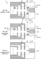
- Figs. 1A to 1C are explanatory diagrams of a wireless communication module 1 according to a first embodiment.
- Fig. 1A is a top view of the wireless communication module 1 of the first embodiment, and here, a semiconductor chip 20 mounted on an antenna substrate 10 is illustrated transparently.
- Fig. 1B is an explanatory diagram of a state at the time of producing the wireless communication module 1 according to the first embodiment.
- Fig. 1C is a diagram illustrating a cross section taken along A-A in Fig. 1A .
- the direction perpendicular to a substrate surface of the antenna substrate 10 is referred to as the "up-down direction”
- the side of the semiconductor chip 20 as viewed from the antenna substrate 10 is referred to as "up”
- the opposite side is referred to as “down”, in some cases.
- the wireless communication module 1 of the first embodiment is a module that performs wireless communication in a millimeter wave band (30 to 300 GHz).
- the wireless communication module 1 includes the antenna substrate 10 and the semiconductor chip 20.
- the semiconductor chip 20 is flip-chip mounted on the antenna substrate 10.
- conductive paste 31 is used to electrically connect the antenna substrate 10 and the semiconductor chip 20.
- the antenna substrate 10 is a substrate (first substrate) on which the semiconductor chip 20 is mounted.
- the antenna substrate 10 includes a substrate body 11, a wiring pattern 12, and substrate-side pads 13.
- the wiring pattern 12 and the substrate-side pads 13 are formed on an upper surface of the substrate body 11.
- a region where the semiconductor chip 20 is mounted (a chip mounting region: a region indicated by dotted lines in Fig. 1A ) is provided.
- a material having a small dielectric loss tangent is desirably used for the substrate body 11. This is because, in a case of the wireless communication module 1 that operates at a high frequency in the millimeter wave band (30 to 300 GHz), the greater the frequency is, the greater the conductor loss and the dielectric loss become. Hence it is necessary to design the wireless communication module 1 in such a manner as to suppress conductor loss and dielectric loss.
- the wiring pattern 12 is a pattern constituting wiring and is formed on the substrate body 11.
- the wiring pattern 12 is formed on the upper surface of the substrate body 11, but the wiring pattern 12 may be formed inside the substrate body 11 or on a lower surface of the substrate body 11.
- the wiring pattern 12 includes a signal line for transmitting a signal, ground wiring serving a ground potential, and the like.
- the wiring pattern 12 of the present embodiment also includes an antenna pattern 12A.
- the substrate-side pads 13 are pads for electrically connecting with the semiconductor chip 20.
- the substrate-side pads 13 are mainly provided on the wiring pattern 12 and are provided inside the chip mounting region on the upper surface of the substrate body 11.
- the wiring pattern 12 and the substrate-side pads 13 of the present embodiment are made of X-ray absorbent materials (materials that have high X-ray absorption). Specifically, the wiring pattern 12 and the substrate-side pads 13 are made of, for example, copper, copper alloy, or the like.
- the wiring pattern 12 may be formed by applying gold plating to copper wiring.
- the wiring pattern 12 and the substrate-side pads 13 of the present embodiment are detectable by X-ray inspection.
- the semiconductor chip 20 is a substrate (second substrate) mounted on the antenna substrate 10 (first substrate).
- the semiconductor chip 20 is a so-called RFIC chip. Since the semiconductor chip 20 that operates at a high frequency, such as an RFIC chip, may possibly deteriorate in characteristics due to the influence of the wiring and the like on the antenna substrate 10, a space is provided between the antenna substrate 10 and the semiconductor chip 20 in the present embodiment. In this manner, this structure maintains the distance between the antenna substrate 10 and the semiconductor chip 20 at a predetermined distance, and thus suppresses transmission loss due to dielectric characteristics.
- a plurality of chip-side pads 21 are provided on the lower surface of the semiconductor chip 20.
- the chip-side pads 21 are pads (connecting terminals) provided on the semiconductor chip 20 and for electrically connecting with the substrate-side pads 13.
- the chip-side pads 21 not provided with the spacers 41 and the corresponding substrate-side pads 13 are bonded with the conductive paste 31.
- the chip-side pads 21 of the present embodiment are constituted to absorb less X-rays than the substrate-side pads 13 and are hence constituted to be difficult to detect by X-ray inspection as compared with the substrate-side pads 13.
- the chip-side pads 21 are made, for example, of aluminum or the like.
- the conductive paste 31 is a pasty conductive member that electrically connects the antenna substrate 10 and the semiconductor chip 20 with each other.
- the conductive paste 31 before curing is a pasty member and is hence a relatively soft member.
- the conductive paste 31 also functions as a bonding member that mechanically bonds the antenna substrate 10 and the semiconductor chip 20 by curing.
- the conductive paste 31 is made, for example, of a curable resin (conductive adhesive) in which conductive particles are dispersed. Since the conductive paste 31 is constituted with conductive metallic particles being dispersed, the conductive paste 31 is a member that is difficult to detect by X-ray inspection compared with the substrate-side pads 13.
- Figs. 5A and 5B are explanatory diagrams of a comparative example.
- Fig. 5A is an explanatory diagram before an antenna substrate 10 and a semiconductor chip 20 are bonded.
- Fig. 5B is an explanatory diagram after the antenna substrate 10 and the semiconductor chip 20 are bonded and is an explanatory diagram of a structure of a wireless communication module 1 according to the comparative embodiment.
- substrate-side pads 13 of the antenna substrate 10 and chip-side pads 21 of the semiconductor chip 20 are bonded with conductive paste 31 without sandwiching any spacers 41 between the substrate-side pads 13 and the chip-side pads 21.
- conductive paste 31 By employing such a bonding method using the conductive paste 31, it is possible to electrically connect two substrates (the antenna substrate 10 and the semiconductor chip 20) at a low temperature with a low load as compared with solder bonding or ultrasonic bonding.
- the two substrates (the antenna substrate 10 and the semiconductor chip 20) are electrically connected with a soft pasty material, and this consequently makes it difficult to maintain the distance between the two substrates (the distance indicated by the arrows in the drawing) at the predetermined distance.
- the antenna substrate 10 is made of the material having a low dielectric loss tangent in order to suppress loss during high-frequency operation
- the characteristics of the semiconductor chip 20 may still possibly be deteriorated due to the influence of the wiring on the antenna substrate 10 during high-frequency operation.
- the conductive paste 31 since the conductive paste 31 is soft, it is extremely difficult to set a load (load applied between the two substrates) such that the distance between the antenna substrate 10 and the semiconductor chip 20 is 50 ⁇ m.
- the spacers 41 are provided in order to facilitate maintaining the distance between the two substrates at the predetermined distance at the time of bonding the two substrates (the antenna substrate 10 and the semiconductor chip 20).
- the spacers 41 are members that define the distance between the two substrates to the predetermined distance.
- the spacers 41 are provided by being sandwiched between the substrate-side pads 13A of the antenna substrate 10 and the chip-side pads 21 of the semiconductor chip 20, to thereby define the distance between the antenna substrate 10 and the semiconductor chip 20 to the predetermined distance.
- the spacers 41 are formed on the chip-side pads 21.
- the spacers 41 can be formed as bumps (spacer bumps) (the spacers 41 can be formed in the same manner as bumps) .
- the spacers 41 are formed as copper pillars or gold stud bumps.
- the spacers 41 are copper pillars
- a manufacturer of the semiconductor chip 20 produces the semiconductor chip 20 on which the copper pillars are formed in advance on the chip-side pads 21, and a module manufacturer who purchased the semiconductor chip 20 with the spacers 41 being already formed produces the wireless communication module 1 as illustrated in Fig. 1B .
- the spacers 41 are gold stud bumps
- the module manufacturer can attach the spacers 41 to the chip-side pads 21 of the semiconductor chip 20 later.
- the spacers 41 are provided on the chip-side pads 21, lower ends of the spacers 41 (end portions of the spacers 41, the end portions being opposite to the chip-side pads 21) protrude below the chip-side pads 21, on the lower surface of the semiconductor chip 20 as illustrated in Fig. 1B .
- the semiconductor chip 20 is brought close to the antenna substrate 10 in a state where the lower ends of the spacers 41 are directed toward the antenna substrate 10, to cause the lower ends of the spacers 41 to abut against (contact) the substrate-side pads 13A of the antenna substrate 10, as illustrated in Fig. 1B .
- the conductive paste 31 is applied in advance to the substrate-side pads 13 to be electrically connected to the chip-side pads 21.
- the conductive paste 31 is arranged between the substrate-side pads 13 of the antenna substrate 10 and the chip-side pads 21 of the semiconductor chip 20, and also the spacers 41 are sandwiched between the two substrates, as illustrated in Fig. 1C .
- the load applied between the antenna substrate 10 and the semiconductor chip 20 changes when the lower ends of the spacers 41 come to contact the antenna substrate 10 (the substrate-side pads 13A of the antenna substrate 10).
- the distance between the two substrates results in a distance (predetermined distance) corresponding to the height (thickness) of the spacers 41.
- the conductive paste 31 is cured after the lower ends of the spacers 41 abut against the substrate-side pads 13A of the antenna substrate 10, whereby the substrate-side pads 13 and the chip-side pads 21 are bonded with the conductive paste 31.
- the substrate-side pads 13 and the chip-side pads 21 not sandwiching the spacers 41 are bonded with the conductive paste 31 in a state where the spacers 41 are sandwiched between other pads of the two substrates as illustrated in Fig. 1C , which prevents the soft pasty conductive paste 31 from being crushed and makes it possible to maintain the distance between the two substrates at the predetermined distance.
- the spacers 41 are provided on the three chip-side pads 21 of the semiconductor chip 20. In this way, it is desirable that three spacers 41 be provided and that, on a straight line connecting two of the spacers 41, the other spacer 41 be not arranged. With this, it is possible to stabilize the posture of the semiconductor chip 20 with respect to the antenna substrate 10 at the time of bonding and to facilitate maintaining the distance between the two substrates (the antenna substrate 10 and the semiconductor chip 20) at the predetermined distance.
- the number of spacers 41 is not limited to three and may be four or more. Even in a case that four or more spacers 41 are provided, it is desirable that, on a straight line connecting two of the spacers 41, the other spacers 41 be not arranged.
- the number of spacers 41 may be less than three (one or two). Even if the number of spacers 41 is one, the load applied between the antenna substrate 10 and the semiconductor chip 20 changes when the lower end of the spacer 41 comes into contact with the corresponding substrate-side pad 13A of the antenna substrate 10, whereby detection of the contact is possible. In a case that the number of spacers 41 is less than three, by bringing the spacer (s) 41 into contact with the antenna substrate 10 while maintaining the semiconductor chip 20 to be parallel with the antenna substrate 10, the distance between the two substrates (the antenna substrate 10 and the semiconductor chip 20) can be maintained at the predetermined distance. With at least two spacers 41, it is possible to determine whether the positional relationship between the antenna substrate 10 and the semiconductor chip 20 at the time of X-ray inspection is normal or abnormal.
- pads (the substrate-side pads 13 and the chip-side pads 21) to be electrically connected with the conductive paste 31 are desirably arranged in a region surrounded by the three or more spacers 41.
- the three or more spacers 41 are desirably arranged on an outer side of the lower surface of the semiconductor chip 20 if possible. This facilitates stabilizing the posture of the semiconductor chip 20 with respect to the antenna substrate 10 at the time of bonding.
- a number of chip-side pads 21 are provided on the lower surface of the semiconductor chip 20, and a plurality of the chip-side pads 21 are constituted as ground pads.
- the spacers 41 are provided on such ground chip-side pads 21. Hence, even when the spacers 41 are provided on the chip-side pads 21, this does not affect operations of the semiconductor chip 20.
- the spacers 41 contact the substrate-side pads 13A provided on the upper surface of the substrate body 11. In this way, the substrate-side pads 13 and the chip-side pads 21 can be spaced from each other for the height (thickness) of the spacers 41, which makes it possible to maintain the distance between the antenna substrate 10 and the semiconductor chip 20 at the predetermined distance.
- the substrate-side pads 13A which the spacers 41 contact may be connected to ground wiring or may be independent of the wiring pattern 12.
- the substrate-side pads 13A (inspection pads 13A) which the spacers 41 contact are also used in X-ray inspection. Accordingly, the substrate-side pads 13A (inspection pads 13A) which the spacers 41 contact, as the other substrate-side pads 13, are made of an X-ray absorbent material (a material that has high X-ray absorption), and are hence detectable in X-ray inspection. In this way, the substrate-side pads 13A which the spacers 41 contact can function as alignment marks.
- the substrate-side pads 13A (inspection pads 13A) which the spacers 41 contact are formed to be larger than the spacers 41 when viewed in an examination direction in X-ray inspection (direction perpendicular to the antenna substrate 10) to facilitate X-ray inspection.
- the diameter of the inspection pads 13A is greater than the diameter of the spacers 41.
- Figs. 2A and 2B illustrate images (X-ray inspection images) at the time when the wireless communication module 1 of the first embodiment is examined in X-ray inspection.
- Fig. 2A is an X-ray inspection image in a case that the positional relationship between the antenna substrate 10 and the semiconductor chip 20 is normal.
- Fig. 2B is an X-ray inspection image in a case that the positional relationship between the antenna substrate 10 and the semiconductor chip 20 is abnormal.
- members detected in X-ray inspection are shaded by hatching.
- the members detected in X-ray inspection include the wiring pattern 12 (also including the antenna pattern 12A), the substrate-side pads 13 (also including the inspection pads 13A), and the spacers 41. Note that the chip-side pads 21 and the conductive paste 31, which have low X-ray absorption, do not appear in an X-ray inspection image.
- the diameter of the inspection pads 13A is greater than the diameter of the spacers 41, it is possible to determine that the positional relationship between the antenna substrate 10 and the semiconductor chip 20 is normal when the smaller-circular images indicating the spacers 41 and the greater-circular images indicating the inspection pads 13A are concentrically arranged (refer to Fig. 2A ). In contrast, it is possible to determine that the positional relationship between the antenna substrate 10 and the semiconductor chip 20 is abnormal when the small-circular images indicating the spacers 41 are deviated from the central positions of the great-circular images indicating the inspection pads 13A. In this way, with the inspection pads 13A having a greater diameter than the diameter of the spacers 41, X-ray inspection can be facilitated.
- Fig. 2C illustrates an X-ray inspection image of the comparative example without the spacers 41.
- the position of the semiconductor chip 20 is not detectable on the basis of an X-ray inspection image as illustrated in Fig. 2C .
- the spacers 41 are provided on the chip-side pads 21 of the semiconductor chip 20, whereby an effect is achieved that the positional relationship between the antenna substrate 10 and the semiconductor chip 20 is detectable on the basis of an X-ray inspection image as illustrated in Figs. 2A and 2B . Note that this effect is an effect in different aspect (remarkable effect) in comparison with an effect as the spacers 41 for defining the distance between the two substrates at the predetermined distance.
- the spacers 41 are constituted to be detectable in X-ray inspection in the present embodiment.
- the spacers 41 are constituted so as to be easily detected in X-ray inspection compared with the chip-side pads 21.
- I 0 denotes an intensity of incident rays (gamma rays).
- I denotes an intensity after passing through an absorption layer.
- d denotes the thickness of the absorption layer.
- ⁇ denotes an absorption coefficient.
- ⁇ denotes a density.
- ⁇ denotes an absorption coefficient at the time when the thickness d of the absorption layer is expressed by mass per area.
- the spacers 41 are desirably made of a material having a higher mass absorption coefficient ( ⁇ / ⁇ ) than that of the chip-side pads 21.
- the spacers 41 are made of copper, gold, or the like, for example.
- the spacers 41 may be formed thicker than the chip-side pads 21.
- the spacers 41 are attached to the chip-side pads 21.
- the spacers 41 may be attached to at least either of the substrate-side pads 13 and the chip-side pads 21.
- the spacers 41 are attached to both the substrate-side pads 13 and the chip-side pads 21.
- Figs. 3A to 3C are explanatory diagrams of a wireless communication module 1 according to the second embodiment.
- Fig. 3A is a top view of the wireless communication module 1 according to the second embodiment, and here, the semiconductor chip 20 mounted on the antenna substrate 10 is illustrated transparently.
- Fig. 3A illustrates an image (X-ray inspection image) at the time when the wireless communication module 1 is examined in X-ray inspection.
- members detected in the X-ray inspection are shaded by hatching.
- Fig. 3B is an explanatory diagram of a state of producing the wireless communication module 1 according to the second embodiment.
- Fig. 3C is a diagram illustrating a cross section taken along B-B in Fig. 3A .
- the spacers 41 are attached to both of the pads, i.e., the substrate-side pads 13 and the chip-side pads 21.
- the upper ends of the spacers 41 attached to the substrate-side pads 13 protrude above the substrate-side pads 13 on the upper surface of the antenna substrate 10
- the lower ends of the spacers 41 attached to the chip-side pads 21 protrude below the chip-side pads 21 on the lower surface of the semiconductor chip 20.
- the upper ends of the spacers 41 attached to the substrate-side pads 13 and the lower ends of the spacers 41 attached to the chip-side pads 21 come to abut against (contact) each other as illustrated in Fig. 3B .
- the conductive paste 31 is applied in advance to the substrate-side pads 13 to be electrically connected to the chip-side pads 21.
- the conductive paste 31 is arranged between the substrate-side pads 13 of the antenna substrate 10 and the chip-side pads 21 of the semiconductor chip 20, and also the spacers 41 are sandwiched between the pads of the two substrates, as illustrated in Fig. 3C .
- the distance between the two substrates is defined to a predetermined distance with the spacers 41, which prevents the soft pasty conductive paste 31 from being crushed.
- the conductive paste 31 is cured, whereby the substrate-side pads 13 and the chip-side pads 21 not sandwiching the spacers 41 are bonded with the conductive paste 31.
- the substrate-side pads 13 and the chip-side pads 21 not sandwiching the spacers 41 are bonded with the conductive paste 31 in a state where the spacers 41 are sandwiched between the substrate-side pads 13A of the antenna substrate 10 and the chip-side pads 21 of the semiconductor chip 20, as illustrated in Fig. 3C .
- the soft pasty conductive paste 31 it is possible to prevent the soft pasty conductive paste 31 from being crushed, and to maintain the distance between the two substrates (the antenna substrate 10 and the semiconductor chip 20) at the predetermined distance.
- the spacers 41 are attached to both pads, i.e., the substrate-side pads 13 and the chip-side pads 21, which makes it possible to maintain the distance between the two substrates (the antenna substrate 10 and the semiconductor chip 20) spaced at a large distance.
- the substrate-side pads 13 and the chip-side pads 21 are miniaturized as the antenna substrate 10 and the semiconductor chip 20 are miniaturized, the height (thickness) of the spacer 41 that can be attached to the pads may be limited.
- the spacers 41 be attached to both the substrate-side pads 13 and the chip-side pads 21.
- the spacers 41 are formed by stacking a metal layer on the pads such as copper pillars, the height of the spacers 41 depends on the area of the pads.
- the spacers 41 that can be stacked on the pads result in being low in height, and therefore, it is preferable, in such a situation, that the spacers 41 be attached to both the substrate-side pads 13 and the chip-side pads 21.
- the spacers 41 are constituted to be detectable in X-ray inspection.
- the spacers 41 are constituted to be detectable in X-ray inspection.
- the spacers 41 may be attached to at least either of the substrate-side pads 13 and the chip-side pads 21. In a third embodiment, the spacers 41 are not attached to the chip-side pads 21, but are attached to the substrate-side pads 13.
- Figs. 4A to 4C are explanatory diagrams of a wireless communication module 1 according to the third embodiment.
- Fig. 4A is a top view of the wireless communication module 1 according to the third embodiment, and here, the semiconductor chip 20 mounted on the antenna substrate 10 is illustrated transparently.
- Fig. 4B is an explanatory diagram of a state of manufacturing the wireless communication module 1 according to the third embodiment.
- Fig. 4C is a diagram illustrating a cross section taken along C-C in Fig. 4A .
- the spacers 41 are attached to the substrate-side pads 13 in the third embodiment.
- the upper ends of the spacers 41 protrude above the substrate-side pads 13 on the upper surface of the antenna substrate 10.
- the conductive paste 31 is applied in advance to the substrate-side pads 13 to be electrically connected to the chip-side pads 21.
- the conductive paste 31 is arranged between the substrate-side pads 13 of the antenna substrate 10 and the chip-side pads 21 of the semiconductor chip 20, and the spacers 41 are sandwiched between the pads of the two substrates, as illustrated in Fig. 4C .
- the distance between the two substrates is defined to the predetermined distance by the spacers 41, which prevents the soft pasty conductive paste 31 from being crushed.
- the semiconductor chip 20 is not provided with any member (e.g., the spacers 41) that can be detected during X-ray inspection.
- the substrate-side pads 13 and the chip-side pads 21 not sandwiching the spacers 41 are bonded with the conductive paste 31 in a state where the spacers 41 are sandwiched between the substrate-side pads 13A of the antenna substrate 10 and the chip-side pads 21 of the semiconductor chip 20, as illustrated in Fig. 4C .
- the wireless communication module including the antenna substrate 10 (first substrate) including an antenna and the semiconductor chip 20 (second substrate) controlling the antenna has been described.
- a substrate module including two substrates is not limited to a wireless communication module including an antenna.
- the techniques of the above-described embodiments are also applicable to a substrate module that includes a first substrate including a plurality of first pads and a second substrate including a plurality of second pads and electrically connecting the first substrate and the second substrate with each other.
- the spacer (s) 41 is attached to at least either of the first pads and the second pads, and the first pads and the second pads not sandwiching the spacer(s) 41 are bonded by the conductive paste 31 in a state where the spacer(s) 41 is sandwiched between the first pad(s) and the second pad(s), it is possible to prevent the soft pasty conductive paste 31 from being crushed and to maintain the distance between the two substrates at a predetermined distance.
- the wireless communication module 1 operating at a high frequency of a millimeter wave band (30 to 300 GHz) as in the above-described embodiments, however, the characteristics of the semiconductor chip 20 (RFIC) operating at a high frequency may possibly be deteriorated due to the influence of the wiring on the antenna substrate 10, and hence, it is desirable to maintain the semiconductor chip 20 at the predetermined distance from the antenna substrate 10.
- the structure in which the first pads and the second pads are bonded with the conductive paste 31 in a state where the spacers 41 are sandwiched between the first substrate and the second substrate is desirably used in the wireless communication module 1 in particular.
Landscapes
- Engineering & Computer Science (AREA)
- Microelectronics & Electronic Packaging (AREA)
- Manufacturing & Machinery (AREA)
- Wire Bonding (AREA)
- Electric Connection Of Electric Components To Printed Circuits (AREA)
- Combinations Of Printed Boards (AREA)
Abstract


Description
- The present invention relates to a substrate module and a method for producing the substrate module.
- Wireless communication modules that perform wireless communication by using an antenna are known. For example,
Patent Literature 1 describes a wireless communication module including a wiring substrate and an RFIC chip laminated and bonded to the wiring substrate. - Patent Literature 1:
JP 2014-150102A - In the wireless communication module described in
Patent Literature 1, a first substrate and a second substrate are bonded by using cored solder balls. Thus, inPatent Literature 1, the distance between the first substrate and the second substrate is maintained at a predetermined distance while the height of the first substrate and the second substrate is utilized for the wiring length of an antenna, which allows the antenna to have a long wiring length. - However, as described in
Patent Literature 1, when two substrates are electrically connected using solder, it is necessary to melt the solder and is therefore necessary to heat the substrates. For this reason, a mounting method using solder is unsuitable for substrates having low heat resistance. - It is also known to electrically connect two substrates by using ultrasonic waves. However, ultrasonic bonding is unsuitable for substrates having low durability because a high load is applied to the substrates.
- A mounting method using conductive paste for substrates having low heat resistance and low durability is known. By employing the mounting method using conductive paste, two substrates can be electrically connected at a low temperature with a low load.
- However, in a case of using conductive paste, the two substrates are electrically connected by a soft pasty material, which makes it difficult to maintain the distance between the two substrates at a predetermined distance as in
Patent Literature 1. - An objective of the present invention is to electrically connect two substrates by using conductive paste while maintaining the distance between the two substrates at a predetermined distance.
- A main aspect of the invention to achieve the above objective is a substrate module comprising: a first substrate including a plurality of first pads; and a second substrate including a plurality of second pads, the first substrate and the second substrate being electrically connected, wherein a spacer is attached to a pad of at least either of the first pads and the second pads, and one or more pairs of the first pads and the second pads not sandwiching the spacer are bonded with conductive paste in a state where the spacer is sandwiched between another pair of the first pads and the second pads.
- Other features of the invention are made clear by the following description and the drawings.
- With some embodiments of the present invention, it is possible to electrically connect two substrates by using conductive paste while maintaining the distance between the two substrates at a predetermined distance.
-
- [
Fig. 1] Figs. 1A to 1C are explanatory diagrams of awireless communication module 1 according to a first embodiment. - [
Fig. 2] Figs. 2A and 2B illustrate X-ray inspection images of thewireless communication module 1 according to the first embodiment.Fig. 2C illustrates an X-ray inspection image in a case of a comparative example withoutspacers 41. - [
Fig. 3] Figs. 3A to 3C are explanatory diagrams of awireless communication module 1 according to a second embodiment. - [
Fig. 4] Figs. 4A to 4C are explanatory diagrams of awireless communication module 1 according to a third embodiment. - [
Fig. 5] Figs. 5A and 5B are explanatory diagrams of the comparative example. - At least the following matters are made clear from the following description and the drawings.
- A substrate module will become clear comprising: a first substrate including a plurality of first pads; and a second substrate including a plurality of second pads, the first substrate and the second substrate being electrically connected, wherein a spacer is attached to a pad of at least either of the first pads and the second pads, and one or more pairs of the first pads and the second pads not sandwiching the spacer are bonded with conductive paste in a state where the spacer is sandwiched between another pair of the first pads and the second pads. According to such a substrate module, it is possible to electrically connect the two substrates by using the conductive paste while maintaining the distance between the two substrates at a predetermined distance.
- A plurality of the spacers are preferably attached to two pads of at least either of the first pads and the second pads. In this way, the positional relationship between the two substrates can be examined.
- The pad to which the spacer is attached is preferably a ground pad. This eliminates any influence on operations.
- The spacer is preferably constituted to be detectable in X-ray inspection. This allows the use of the spacer in X-ray inspection.
- The first pads are preferably constituted to be detectable in X-ray inspection; and the spacer is preferably attached to a pad of the second pads. In this way, the positional relationship between the first substrate and the second substrate can be examined on the basis of the positional relationship between an image indicating the first pad and an image indicating the spacer in an X-ray inspection image.
- A pad of the first pads sandwiching the spacer is preferably larger than the spacer when viewed from an examination direction in the X-ray inspection. This facilitates an X-ray inspection.
- The spacers are preferably attached to a pad of the first pads and a pad of the second pads; an end portion of one of the spacers attached to the pad of the first pads and an end portion of another of the spacers attached to the pad of the second pads are preferably in contact with each other, the end portion of one of the spacers attached to the pad of the first pads being opposite to the first pads, the end portion of another of the spacers attached to the pad of the second pads being opposite to the second pads. In this way, it is possible to maintain the two substrates spaced at a large distance.
- The spacer is preferably formed by stacking a metal layer. In such a case, a structure in which the spacer is attached to each of the first pad and the second pad is particularly advantageous.
- The first substrate is preferably a wiring substrate including an antenna; and the second substrate is preferably a semiconductor chip for controlling the antenna. In this way, it is possible to suppress deterioration of the characteristics of the semiconductor chip due to the influence of the wiring substrate when the semiconductor chip operates at a high frequency.
- A method for producing a substrate module, the method preferably comprising: preparing a first substrate including a plurality of first pads and a second substrate including a plurality of second pads; and electrically connecting the first substrate and the second substrate, wherein preferably a spacer is attached to a pad of at least either of the first pads and the second pads, and one or more pairs of the first pads and the second pads not sandwiching the spacer are bonded with conductive paste in a state where the spacer is sandwiched between another pair of the first pads and the second pads. With such a method for producing a substrate module, it is possible to electrically connect the two substrates by using conductive paste while maintaining the distance between the two substrates at a predetermined distance.
-
Figs. 1A to 1C are explanatory diagrams of awireless communication module 1 according to a first embodiment.Fig. 1A is a top view of thewireless communication module 1 of the first embodiment, and here, asemiconductor chip 20 mounted on anantenna substrate 10 is illustrated transparently.Fig. 1B is an explanatory diagram of a state at the time of producing thewireless communication module 1 according to the first embodiment.Fig. 1C is a diagram illustrating a cross section taken along A-A inFig. 1A . Note that, in the following description, the direction perpendicular to a substrate surface of theantenna substrate 10 is referred to as the "up-down direction", the side of thesemiconductor chip 20 as viewed from theantenna substrate 10 is referred to as "up", and the opposite side is referred to as "down", in some cases. - The
wireless communication module 1 of the first embodiment is a module that performs wireless communication in a millimeter wave band (30 to 300 GHz). Thewireless communication module 1 includes theantenna substrate 10 and thesemiconductor chip 20. Thesemiconductor chip 20 is flip-chip mounted on theantenna substrate 10. In the present embodiment,conductive paste 31 is used to electrically connect theantenna substrate 10 and thesemiconductor chip 20. - The
antenna substrate 10 is a substrate (first substrate) on which thesemiconductor chip 20 is mounted. Theantenna substrate 10 includes asubstrate body 11, awiring pattern 12, and substrate-side pads 13. - The
wiring pattern 12 and the substrate-side pads 13 are formed on an upper surface of thesubstrate body 11. In addition, on the upper surface of thesubstrate body 11, a region where thesemiconductor chip 20 is mounted (a chip mounting region: a region indicated by dotted lines inFig. 1A ) is provided. Note that a material having a small dielectric loss tangent is desirably used for thesubstrate body 11. This is because, in a case of thewireless communication module 1 that operates at a high frequency in the millimeter wave band (30 to 300 GHz), the greater the frequency is, the greater the conductor loss and the dielectric loss become. Hence it is necessary to design thewireless communication module 1 in such a manner as to suppress conductor loss and dielectric loss. - The
wiring pattern 12 is a pattern constituting wiring and is formed on thesubstrate body 11. Here, thewiring pattern 12 is formed on the upper surface of thesubstrate body 11, but thewiring pattern 12 may be formed inside thesubstrate body 11 or on a lower surface of thesubstrate body 11. Thewiring pattern 12 includes a signal line for transmitting a signal, ground wiring serving a ground potential, and the like. Thewiring pattern 12 of the present embodiment also includes anantenna pattern 12A. - The substrate-
side pads 13 are pads for electrically connecting with thesemiconductor chip 20. The substrate-side pads 13 are mainly provided on thewiring pattern 12 and are provided inside the chip mounting region on the upper surface of thesubstrate body 11. - The
wiring pattern 12 and the substrate-side pads 13 of the present embodiment are made of X-ray absorbent materials (materials that have high X-ray absorption). Specifically, thewiring pattern 12 and the substrate-side pads 13 are made of, for example, copper, copper alloy, or the like. Thewiring pattern 12 may be formed by applying gold plating to copper wiring. Thewiring pattern 12 and the substrate-side pads 13 of the present embodiment are detectable by X-ray inspection. - The
semiconductor chip 20 is a substrate (second substrate) mounted on the antenna substrate 10 (first substrate). In the present embodiment, thesemiconductor chip 20 is a so-called RFIC chip. Since thesemiconductor chip 20 that operates at a high frequency, such as an RFIC chip, may possibly deteriorate in characteristics due to the influence of the wiring and the like on theantenna substrate 10, a space is provided between theantenna substrate 10 and thesemiconductor chip 20 in the present embodiment. In this manner, this structure maintains the distance between theantenna substrate 10 and thesemiconductor chip 20 at a predetermined distance, and thus suppresses transmission loss due to dielectric characteristics. - A plurality of chip-
side pads 21 are provided on the lower surface of thesemiconductor chip 20. The chip-side pads 21 are pads (connecting terminals) provided on thesemiconductor chip 20 and for electrically connecting with the substrate-side pads 13. In the present embodiment, the chip-side pads 21 not provided with thespacers 41 and the corresponding substrate-side pads 13 are bonded with theconductive paste 31. - Note that the chip-
side pads 21 of the present embodiment are constituted to absorb less X-rays than the substrate-side pads 13 and are hence constituted to be difficult to detect by X-ray inspection as compared with the substrate-side pads 13. The chip-side pads 21 are made, for example, of aluminum or the like. - The
conductive paste 31 is a pasty conductive member that electrically connects theantenna substrate 10 and thesemiconductor chip 20 with each other. Theconductive paste 31 before curing is a pasty member and is hence a relatively soft member. However, theconductive paste 31 also functions as a bonding member that mechanically bonds theantenna substrate 10 and thesemiconductor chip 20 by curing. Theconductive paste 31 is made, for example, of a curable resin (conductive adhesive) in which conductive particles are dispersed. Since theconductive paste 31 is constituted with conductive metallic particles being dispersed, theconductive paste 31 is a member that is difficult to detect by X-ray inspection compared with the substrate-side pads 13. -
Figs. 5A and 5B are explanatory diagrams of a comparative example.Fig. 5A is an explanatory diagram before anantenna substrate 10 and asemiconductor chip 20 are bonded.Fig. 5B is an explanatory diagram after theantenna substrate 10 and thesemiconductor chip 20 are bonded and is an explanatory diagram of a structure of awireless communication module 1 according to the comparative embodiment. - In the comparative example, substrate-
side pads 13 of theantenna substrate 10 and chip-side pads 21 of thesemiconductor chip 20 are bonded withconductive paste 31 without sandwiching anyspacers 41 between the substrate-side pads 13 and the chip-side pads 21. By employing such a bonding method using theconductive paste 31, it is possible to electrically connect two substrates (theantenna substrate 10 and the semiconductor chip 20) at a low temperature with a low load as compared with solder bonding or ultrasonic bonding. However, in a case that theconductive paste 31 is used, the two substrates (theantenna substrate 10 and the semiconductor chip 20) are electrically connected with a soft pasty material, and this consequently makes it difficult to maintain the distance between the two substrates (the distance indicated by the arrows in the drawing) at the predetermined distance. Moreover, it is difficult to control the load applied between the two substrates at the time of bonding for maintaining the distance between the two substrates (the distance indicated by the arrows in the drawing) at the predetermined distance. - Incidentally, as has already been described, although the
antenna substrate 10 is made of the material having a low dielectric loss tangent in order to suppress loss during high-frequency operation, the characteristics of the semiconductor chip 20 (RFIC) may still possibly be deteriorated due to the influence of the wiring on theantenna substrate 10 during high-frequency operation. In view of this, it is desirable to maintain the distance between theantenna substrate 10 and thesemiconductor chip 20 at the predetermined distance so that theantenna substrate 10 and thesemiconductor chip 20 do not come too close to each other, and in the present embodiment, the distance between theantenna substrate 10 and thesemiconductor chip 20 is assumed to be 50 µm or greater. However, in the bonding method described in the comparative example, since theconductive paste 31 is soft, it is extremely difficult to set a load (load applied between the two substrates) such that the distance between theantenna substrate 10 and thesemiconductor chip 20 is 50 µm. - In view of this, in the present embodiment, the spacers 41 (refer to
Figs. 1B and 1C ) are provided in order to facilitate maintaining the distance between the two substrates at the predetermined distance at the time of bonding the two substrates (theantenna substrate 10 and the semiconductor chip 20). - The
spacers 41 are members that define the distance between the two substrates to the predetermined distance. In the present embodiment, thespacers 41 are provided by being sandwiched between the substrate-side pads 13A of theantenna substrate 10 and the chip-side pads 21 of thesemiconductor chip 20, to thereby define the distance between theantenna substrate 10 and thesemiconductor chip 20 to the predetermined distance. - The
spacers 41 are formed on the chip-side pads 21. By providing thespacers 41 on the chip-side pads 21, thespacers 41 can be formed as bumps (spacer bumps) (thespacers 41 can be formed in the same manner as bumps) . For example, thespacers 41 are formed as copper pillars or gold stud bumps. In a case that thespacers 41 are copper pillars, a manufacturer of thesemiconductor chip 20 produces thesemiconductor chip 20 on which the copper pillars are formed in advance on the chip-side pads 21, and a module manufacturer who purchased thesemiconductor chip 20 with thespacers 41 being already formed produces thewireless communication module 1 as illustrated inFig. 1B . In a case that thespacers 41 are gold stud bumps, in contrast, the module manufacturer can attach thespacers 41 to the chip-side pads 21 of thesemiconductor chip 20 later. - Since the
spacers 41 are provided on the chip-side pads 21, lower ends of the spacers 41 (end portions of thespacers 41, the end portions being opposite to the chip-side pads 21) protrude below the chip-side pads 21, on the lower surface of thesemiconductor chip 20 as illustrated inFig. 1B . When theantenna substrate 10 and thesemiconductor chip 20 are bonded, thesemiconductor chip 20 is brought close to theantenna substrate 10 in a state where the lower ends of thespacers 41 are directed toward theantenna substrate 10, to cause the lower ends of thespacers 41 to abut against (contact) the substrate-side pads 13A of theantenna substrate 10, as illustrated inFig. 1B . Note that, as illustrated inFig. 1B , theconductive paste 31 is applied in advance to the substrate-side pads 13 to be electrically connected to the chip-side pads 21. - When the lower ends of the
spacers 41 abut against the substrate-side pads 13A of theantenna substrate 10, theconductive paste 31 is arranged between the substrate-side pads 13 of theantenna substrate 10 and the chip-side pads 21 of thesemiconductor chip 20, and also thespacers 41 are sandwiched between the two substrates, as illustrated inFig. 1C . As illustrated inFig. 1C , the load applied between theantenna substrate 10 and thesemiconductor chip 20 changes when the lower ends of thespacers 41 come to contact the antenna substrate 10 (the substrate-side pads 13A of the antenna substrate 10). Hence, by stopping the approach between theantenna substrate 10 and thesemiconductor chip 20 at the stage when the change of the load is detected, the distance between the two substrates results in a distance (predetermined distance) corresponding to the height (thickness) of thespacers 41. Note that theconductive paste 31 is cured after the lower ends of thespacers 41 abut against the substrate-side pads 13A of theantenna substrate 10, whereby the substrate-side pads 13 and the chip-side pads 21 are bonded with theconductive paste 31. According to the present embodiment, the substrate-side pads 13 and the chip-side pads 21 not sandwiching thespacers 41 are bonded with theconductive paste 31 in a state where thespacers 41 are sandwiched between other pads of the two substrates as illustrated inFig. 1C , which prevents the soft pastyconductive paste 31 from being crushed and makes it possible to maintain the distance between the two substrates at the predetermined distance. - In the present embodiment, the
spacers 41 are provided on the three chip-side pads 21 of thesemiconductor chip 20. In this way, it is desirable that threespacers 41 be provided and that, on a straight line connecting two of thespacers 41, theother spacer 41 be not arranged. With this, it is possible to stabilize the posture of thesemiconductor chip 20 with respect to theantenna substrate 10 at the time of bonding and to facilitate maintaining the distance between the two substrates (theantenna substrate 10 and the semiconductor chip 20) at the predetermined distance. However, the number ofspacers 41 is not limited to three and may be four or more. Even in a case that four ormore spacers 41 are provided, it is desirable that, on a straight line connecting two of thespacers 41, theother spacers 41 be not arranged. - Note that the number of
spacers 41 may be less than three (one or two). Even if the number ofspacers 41 is one, the load applied between theantenna substrate 10 and thesemiconductor chip 20 changes when the lower end of thespacer 41 comes into contact with the corresponding substrate-side pad 13A of theantenna substrate 10, whereby detection of the contact is possible. In a case that the number ofspacers 41 is less than three, by bringing the spacer (s) 41 into contact with theantenna substrate 10 while maintaining thesemiconductor chip 20 to be parallel with theantenna substrate 10, the distance between the two substrates (theantenna substrate 10 and the semiconductor chip 20) can be maintained at the predetermined distance. With at least twospacers 41, it is possible to determine whether the positional relationship between theantenna substrate 10 and thesemiconductor chip 20 at the time of X-ray inspection is normal or abnormal. - In a case that three or
more spacers 41 are provided, pads (the substrate-side pads 13 and the chip-side pads 21) to be electrically connected with theconductive paste 31 are desirably arranged in a region surrounded by the three ormore spacers 41. In other words, the three ormore spacers 41 are desirably arranged on an outer side of the lower surface of thesemiconductor chip 20 if possible. This facilitates stabilizing the posture of thesemiconductor chip 20 with respect to theantenna substrate 10 at the time of bonding. - A number of chip-
side pads 21 are provided on the lower surface of thesemiconductor chip 20, and a plurality of the chip-side pads 21 are constituted as ground pads. In the present embodiment, thespacers 41 are provided on such ground chip-side pads 21. Hence, even when thespacers 41 are provided on the chip-side pads 21, this does not affect operations of thesemiconductor chip 20. - The
spacers 41 contact the substrate-side pads 13A provided on the upper surface of thesubstrate body 11. In this way, the substrate-side pads 13 and the chip-side pads 21 can be spaced from each other for the height (thickness) of thespacers 41, which makes it possible to maintain the distance between theantenna substrate 10 and thesemiconductor chip 20 at the predetermined distance. The substrate-side pads 13A which thespacers 41 contact may be connected to ground wiring or may be independent of thewiring pattern 12. - In the present embodiment, the substrate-
side pads 13A (inspection pads 13A) which thespacers 41 contact are also used in X-ray inspection. Accordingly, the substrate-side pads 13A (inspection pads 13A) which thespacers 41 contact, as the other substrate-side pads 13, are made of an X-ray absorbent material (a material that has high X-ray absorption), and are hence detectable in X-ray inspection. In this way, the substrate-side pads 13A which thespacers 41 contact can function as alignment marks. - In the present embodiment, the substrate-
side pads 13A (inspection pads 13A) which thespacers 41 contact are formed to be larger than thespacers 41 when viewed in an examination direction in X-ray inspection (direction perpendicular to the antenna substrate 10) to facilitate X-ray inspection. Specifically, in the present embodiment, the diameter of theinspection pads 13A is greater than the diameter of thespacers 41. -
Figs. 2A and 2B illustrate images (X-ray inspection images) at the time when thewireless communication module 1 of the first embodiment is examined in X-ray inspection.Fig. 2A is an X-ray inspection image in a case that the positional relationship between theantenna substrate 10 and thesemiconductor chip 20 is normal.Fig. 2B is an X-ray inspection image in a case that the positional relationship between theantenna substrate 10 and thesemiconductor chip 20 is abnormal. InFigs. 2A and 2B , members detected in X-ray inspection are shaded by hatching. The members detected in X-ray inspection include the wiring pattern 12 (also including theantenna pattern 12A), the substrate-side pads 13 (also including theinspection pads 13A), and thespacers 41. Note that the chip-side pads 21 and theconductive paste 31, which have low X-ray absorption, do not appear in an X-ray inspection image. - In a case that the positional relationship between the
antenna substrate 10 and thesemiconductor chip 20 is normal (case that thesemiconductor chip 20 is normally mounted on the chip mounting region of the antenna substrate 10), the lower ends of thespacers 41 are in a state of abutting against central positions of theinspection pads 13A (refer toFig. 1C ). Hence, by examining the positional relationship between circular images indicating thespacers 41 and circular images indicating theinspection pads 13A in an X-ray inspection image, it is possible to determine whether the positional relationship between theantenna substrate 10 and thesemiconductor chip 20 is normal or abnormal. In the present embodiment, since the diameter of theinspection pads 13A is greater than the diameter of thespacers 41, it is possible to determine that the positional relationship between theantenna substrate 10 and thesemiconductor chip 20 is normal when the smaller-circular images indicating thespacers 41 and the greater-circular images indicating theinspection pads 13A are concentrically arranged (refer toFig. 2A ). In contrast, it is possible to determine that the positional relationship between theantenna substrate 10 and thesemiconductor chip 20 is abnormal when the small-circular images indicating thespacers 41 are deviated from the central positions of the great-circular images indicating theinspection pads 13A. In this way, with theinspection pads 13A having a greater diameter than the diameter of thespacers 41, X-ray inspection can be facilitated. Note that even if thespacers 41 are larger than theinspection pads 13A, portions where the images indicating thespacers 41 and the images indicating the inspection pads overlap each other appear darker, which enables X-ray inspection. Even if thespacers 41 and theinspection pads 13A have similar sizes, it is possible to determine whether the positional relationship between theantenna substrate 10 and thesemiconductor chip 20 is normal or abnormal, by examining the positional relationship between the images indicating thespacers 41 and the images indicating theinspection pads 13A. -
Fig. 2C illustrates an X-ray inspection image of the comparative example without thespacers 41. In a case that nospacers 41 are attached to the semiconductor chip 20 (refer toFig. 5B ), the position of thesemiconductor chip 20 is not detectable on the basis of an X-ray inspection image as illustrated inFig. 2C . In contrast to this, in the present embodiment, thespacers 41 are provided on the chip-side pads 21 of thesemiconductor chip 20, whereby an effect is achieved that the positional relationship between theantenna substrate 10 and thesemiconductor chip 20 is detectable on the basis of an X-ray inspection image as illustrated inFigs. 2A and 2B . Note that this effect is an effect in different aspect (remarkable effect) in comparison with an effect as thespacers 41 for defining the distance between the two substrates at the predetermined distance. - As illustrated in
Figs. 2A and 2B , thespacers 41 are constituted to be detectable in X-ray inspection in the present embodiment. Hence, thespacers 41 are constituted so as to be easily detected in X-ray inspection compared with the chip-side pads 21. Specifically, thespacers 41 are constituted so as to have a greater intensity I of the following equation than that of the chip-side pads 21.
- In the above equation, I0 denotes an intensity of incident rays (gamma rays). I denotes an intensity after passing through an absorption layer. d denotes the thickness of the absorption layer. µ denotes an absorption coefficient. ρ denotes a density. ω denotes an absorption coefficient at the time when the thickness d of the absorption layer is expressed by mass per area. The
spacers 41 are desirably made of a material having a higher mass absorption coefficient (µ/ρ) than that of the chip-side pads 21. Here, as described above, thespacers 41 are made of copper, gold, or the like, for example. Thespacers 41 may be formed thicker than the chip-side pads 21. - In the first embodiment described above, the
spacers 41 are attached to the chip-side pads 21. However, thespacers 41 may be attached to at least either of the substrate-side pads 13 and the chip-side pads 21. In a second embodiment, thespacers 41 are attached to both the substrate-side pads 13 and the chip-side pads 21. -
Figs. 3A to 3C are explanatory diagrams of awireless communication module 1 according to the second embodiment.Fig. 3A is a top view of thewireless communication module 1 according to the second embodiment, and here, thesemiconductor chip 20 mounted on theantenna substrate 10 is illustrated transparently. In other words,Fig. 3A illustrates an image (X-ray inspection image) at the time when thewireless communication module 1 is examined in X-ray inspection. InFig. 3A , members detected in the X-ray inspection are shaded by hatching.Fig. 3B is an explanatory diagram of a state of producing thewireless communication module 1 according to the second embodiment.Fig. 3C is a diagram illustrating a cross section taken along B-B inFig. 3A . - As illustrated in
Fig. 3B , in the second embodiment, thespacers 41 are attached to both of the pads, i.e., the substrate-side pads 13 and the chip-side pads 21. Hence, as illustrated inFig. 3B , the upper ends of thespacers 41 attached to the substrate-side pads 13 (the end portions of thespacers 41, the end portions being opposite to the substrate-side pads 13) protrude above the substrate-side pads 13 on the upper surface of theantenna substrate 10, and also the lower ends of thespacers 41 attached to the chip-side pads 21 (the end portions of thespacers 41, the end portions being opposite to the chip-side pads 21) protrude below the chip-side pads 21 on the lower surface of thesemiconductor chip 20. At the time of bonding theantenna substrate 10 and thesemiconductor chip 20, the upper ends of thespacers 41 attached to the substrate-side pads 13 and the lower ends of thespacers 41 attached to the chip-side pads 21 come to abut against (contact) each other as illustrated inFig. 3B . Note that, as illustrated inFig. 3B , theconductive paste 31 is applied in advance to the substrate-side pads 13 to be electrically connected to the chip-side pads 21. - When the
spacers 41 abut against each other, theconductive paste 31 is arranged between the substrate-side pads 13 of theantenna substrate 10 and the chip-side pads 21 of thesemiconductor chip 20, and also thespacers 41 are sandwiched between the pads of the two substrates, as illustrated inFig. 3C . Also in the second embodiment, the distance between the two substrates is defined to a predetermined distance with thespacers 41, which prevents the soft pastyconductive paste 31 from being crushed. After the lower ends of thespacers 41 attached to the chip-side pads 21 of thesemiconductor chip 20 abut against the upper ends of thespacers 41 attached to the substrate-side pads 13 of theantenna substrate 10, theconductive paste 31 is cured, whereby the substrate-side pads 13 and the chip-side pads 21 not sandwiching thespacers 41 are bonded with theconductive paste 31. - Also in the second embodiment, the substrate-
side pads 13 and the chip-side pads 21 not sandwiching thespacers 41 are bonded with theconductive paste 31 in a state where thespacers 41 are sandwiched between the substrate-side pads 13A of theantenna substrate 10 and the chip-side pads 21 of thesemiconductor chip 20, as illustrated inFig. 3C . With this, it is possible to prevent the soft pastyconductive paste 31 from being crushed, and to maintain the distance between the two substrates (theantenna substrate 10 and the semiconductor chip 20) at the predetermined distance. - As in the second embodiment, the
spacers 41 are attached to both pads, i.e., the substrate-side pads 13 and the chip-side pads 21, which makes it possible to maintain the distance between the two substrates (theantenna substrate 10 and the semiconductor chip 20) spaced at a large distance. For example, in a case that the substrate-side pads 13 and the chip-side pads 21 are miniaturized as theantenna substrate 10 and thesemiconductor chip 20 are miniaturized, the height (thickness) of thespacer 41 that can be attached to the pads may be limited. Hence, in a case that it is desired to maintain the two substrates (theantenna substrate 10 and the semiconductor chip 20) spaced at a large distance under such a situation, it is desirable that thespacers 41 be attached to both the substrate-side pads 13 and the chip-side pads 21. Specifically, in a case that thespacers 41 are formed by stacking a metal layer on the pads such as copper pillars, the height of thespacers 41 depends on the area of the pads. Hence, if the areas of the substrate-side pads 13 and the chip-side pads 21 are small, thespacers 41 that can be stacked on the pads result in being low in height, and therefore, it is preferable, in such a situation, that thespacers 41 be attached to both the substrate-side pads 13 and the chip-side pads 21. - Also in the second embodiment, the
spacers 41 are constituted to be detectable in X-ray inspection. Hence, by examining, in an X-ray inspection image, the positional relationship between circular images indicating thespacers 41 of the substrate-side pads 13 and circular images indicating thespacers 41 of the chip-side pads 21, it is possible to determine whether the positional relationship between theantenna substrate 10 and thesemiconductor chip 20 is normal or abnormal. For example, in the X-ray inspection image illustrated inFig. 3A , it is possible to determine that the positional relation between theantenna substrate 10 and thesemiconductor chip 20 is normal on the basis of the fact that the circular images indicating thespacers 41 of the substrate-side pads 13 and the circular images indicating thespacers 41 of the chip-side pads 21 overlap with each other. - As has already been described, the
spacers 41 may be attached to at least either of the substrate-side pads 13 and the chip-side pads 21. In a third embodiment, thespacers 41 are not attached to the chip-side pads 21, but are attached to the substrate-side pads 13. -
Figs. 4A to 4C are explanatory diagrams of awireless communication module 1 according to the third embodiment.Fig. 4A is a top view of thewireless communication module 1 according to the third embodiment, and here, thesemiconductor chip 20 mounted on theantenna substrate 10 is illustrated transparently.Fig. 4B is an explanatory diagram of a state of manufacturing thewireless communication module 1 according to the third embodiment.Fig. 4C is a diagram illustrating a cross section taken along C-C inFig. 4A . - As illustrated in
Fig. 4B , thespacers 41 are attached to the substrate-side pads 13 in the third embodiment. Hence, as illustrated inFig. 4B , the upper ends of thespacers 41 protrude above the substrate-side pads 13 on the upper surface of theantenna substrate 10. At the time of bonding theantenna substrate 10 and thesemiconductor chip 20, the upper ends of thespacers 41 and the chip-side pads 21 abut against each other as illustrated inFig. 4B . Note that as illustrated inFig. 4B , theconductive paste 31 is applied in advance to the substrate-side pads 13 to be electrically connected to the chip-side pads 21. - When the upper ends of the
spacers 41 abut against the chip-side pads 21, theconductive paste 31 is arranged between the substrate-side pads 13 of theantenna substrate 10 and the chip-side pads 21 of thesemiconductor chip 20, and thespacers 41 are sandwiched between the pads of the two substrates, as illustrated inFig. 4C . Also in the third embodiment, the distance between the two substrates is defined to the predetermined distance by thespacers 41, which prevents the soft pastyconductive paste 31 from being crushed. After the upper ends of thespacers 41 abut against the chip-side pads 21 of thesemiconductor chip 20, theconductive paste 31 is cured, whereby the substrate-side pads 13 and the chip-side pads 21 not sandwiching the spacers are bonded with theconductive paste 31. - In the third embodiment, the
semiconductor chip 20 is not provided with any member (e.g., the spacers 41) that can be detected during X-ray inspection. Hence, in the structure of the third embodiment, it is difficult to determine the positional relation between theantenna substrate 10 and thesemiconductor chip 20 on the basis of X-ray inspection images (refer toFig. 4A ). However, also in the third embodiment, the substrate-side pads 13 and the chip-side pads 21 not sandwiching thespacers 41 are bonded with theconductive paste 31 in a state where thespacers 41 are sandwiched between the substrate-side pads 13A of theantenna substrate 10 and the chip-side pads 21 of thesemiconductor chip 20, as illustrated inFig. 4C . Hence, also in the third embodiment, it is possible to prevent the soft pastyconductive paste 31 from being crushed and to maintain the distance between the two substrates (theantenna substrate 10 and the semiconductor chip 20) at a predetermined distance. - In each of the above-described embodiments, the wireless communication module including the antenna substrate 10 (first substrate) including an antenna and the semiconductor chip 20 (second substrate) controlling the antenna has been described. However, a substrate module including two substrates is not limited to a wireless communication module including an antenna.
- Specifically, the techniques of the above-described embodiments are also applicable to a substrate module that includes a first substrate including a plurality of first pads and a second substrate including a plurality of second pads and electrically connecting the first substrate and the second substrate with each other. In this case, if the spacer (s) 41 is attached to at least either of the first pads and the second pads, and the first pads and the second pads not sandwiching the spacer(s) 41 are bonded by the
conductive paste 31 in a state where the spacer(s) 41 is sandwiched between the first pad(s) and the second pad(s), it is possible to prevent the soft pastyconductive paste 31 from being crushed and to maintain the distance between the two substrates at a predetermined distance. - In a case of the
wireless communication module 1 operating at a high frequency of a millimeter wave band (30 to 300 GHz) as in the above-described embodiments, however, the characteristics of the semiconductor chip 20 (RFIC) operating at a high frequency may possibly be deteriorated due to the influence of the wiring on theantenna substrate 10, and hence, it is desirable to maintain thesemiconductor chip 20 at the predetermined distance from theantenna substrate 10. In view of this, the structure in which the first pads and the second pads are bonded with theconductive paste 31 in a state where thespacers 41 are sandwiched between the first substrate and the second substrate is desirably used in thewireless communication module 1 in particular. - The foregoing embodiments are for facilitating the understanding of the present invention, and are not to be construed as limiting the present invention. The present invention may be modified and/or improved without departing from the gist thereof, and it goes without saying that the present invention encompasses any equivalents thereof.
-
- 1:
- Wireless communication module;
- 10:
- Antenna substrate (first substrate);
- 11:
- Substrate body;
- 12:
- Wiring pattern;
- 12A:
- Antenna pattern;
- 13:
- Substrate-side pad (first pad);
- 13A:
- Inspection pad;
- 20:
- Semiconductor chip (second substrate);
- 21:
- Chip-side pad (second pad);
- 31:
- Conductive paste;
- 41:
- Spacer.
Claims (10)
- A substrate module comprising:a first substrate including a plurality of first pads; anda second substrate including a plurality of second pads, the first substrate and the second substrate being electrically connected, whereina spacer is attached to a pad of at least either of the first pads and the second pads, andone or more pairs of the first pads and the second pads not sandwiching the spacer are bonded with conductive paste in a state where the spacer is sandwiched between another pair of the first pads and the second pads.
- The substrate module according to claim 1, wherein a plurality of the spacers are attached to two pads of at least either of the first pads and the second pads.
- The substrate module according to claim 1 or 2, wherein the pad to which the spacer is attached is a ground pad.
- The substrate module according to any one of claims 1 to 3, wherein the spacer is constituted to be detectable in X-ray inspection.
- The substrate module according to claim 4, wherein:the first pads are constituted to be detectable in X-ray inspection; andthe spacer is attached to a pad of the second pads.
- The substrate module according to claim 5, wherein a pad of the first pads sandwiching the spacer is larger than the spacer when viewed from an examination direction in the X-ray inspection.
- The substrate module according to any one of claims 1 to 6, wherein:the spacers are attached to a pad of the first pads and a pad of the second pads;an end portion of one of the spacers attached to the pad of the first pads and an end portion of another of the spacers attached to the pad of the second pads are in contact with each other, the end portion of one of the spacers attached to the pad of the first pads being opposite to the first pads, the end portion of another of the spacers attached to the pad of the second pads being opposite to the second pads.
- The substrate module according to claim 7, wherein the spacer is formed by stacking a metal layer.
- The substrate module according to any one of claims 1 to 8, wherein:the first substrate is a wiring substrate including an antenna; andthe second substrate is a semiconductor chip for controlling the antenna.
- A method for producing a substrate module, the method comprising:preparing a first substrate including a plurality of first pads and a second substrate including a plurality of second pads; andelectrically connecting the first substrate and the second substrate, whereina spacer is attached to a pad of at least either of the first pads and the second pads, andone or more pairs of the first pads and the second pads not sandwiching the spacer are bonded with conductive paste in a state where the spacer is sandwiched between another pair of the first pads and the second pads.
Applications Claiming Priority (2)
| Application Number | Priority Date | Filing Date | Title |
|---|---|---|---|
| JP2017132497A JP2019016678A (en) | 2017-07-06 | 2017-07-06 | Substrate module and method for manufacturing substrate module |
| PCT/JP2018/006160 WO2019008816A1 (en) | 2017-07-06 | 2018-02-21 | Substrate module, and method for producing substrate module |
Publications (2)
| Publication Number | Publication Date |
|---|---|
| EP3629367A1 true EP3629367A1 (en) | 2020-04-01 |
| EP3629367A4 EP3629367A4 (en) | 2020-10-14 |
Family
ID=64950850
Family Applications (1)
| Application Number | Title | Priority Date | Filing Date |
|---|---|---|---|
| EP18828625.6A Withdrawn EP3629367A4 (en) | 2017-07-06 | 2018-02-21 | SUBSTRATE MODULE AND METHOD FOR MANUFACTURING A SUBSTRATE MODULE |
Country Status (4)
| Country | Link |
|---|---|
| US (1) | US20200120796A1 (en) |
| EP (1) | EP3629367A4 (en) |
| JP (1) | JP2019016678A (en) |
| WO (1) | WO2019008816A1 (en) |
Families Citing this family (2)
| Publication number | Priority date | Publication date | Assignee | Title |
|---|---|---|---|---|
| KR102528016B1 (en) * | 2018-10-05 | 2023-05-02 | 삼성전자주식회사 | Solder member mounting method and system |
| WO2021250727A1 (en) | 2020-06-08 | 2021-12-16 | オリンパス株式会社 | Electronic module, method for manufacturing electronic module, and endoscope |
Family Cites Families (7)
| Publication number | Priority date | Publication date | Assignee | Title |
|---|---|---|---|---|
| JP2001015552A (en) * | 1999-07-02 | 2001-01-19 | Shinkawa Ltd | Flip chip mounting method |
| KR100698527B1 (en) * | 2005-08-11 | 2007-03-22 | 삼성전자주식회사 | Chip stack package having pillar bumps using metal bumps and method for manufacturing same |
| WO2007109326A2 (en) * | 2006-03-21 | 2007-09-27 | Promerus Llc | Methods and materials useful for chip stacking, chip and wafer bonding |
| JP2008112810A (en) * | 2006-10-30 | 2008-05-15 | Kyocera Corp | Circuit board, semiconductor element storage package, and semiconductor device |
| JP5350604B2 (en) * | 2007-05-16 | 2013-11-27 | スパンション エルエルシー | Semiconductor device and manufacturing method thereof |
| JP4833192B2 (en) * | 2007-12-27 | 2011-12-07 | 新光電気工業株式会社 | Electronic equipment |
| JP6027905B2 (en) | 2013-01-31 | 2016-11-16 | 新光電気工業株式会社 | Semiconductor device |
-
2017
- 2017-07-06 JP JP2017132497A patent/JP2019016678A/en active Pending
-
2018
- 2018-02-21 EP EP18828625.6A patent/EP3629367A4/en not_active Withdrawn
- 2018-02-21 US US16/626,378 patent/US20200120796A1/en not_active Abandoned
- 2018-02-21 WO PCT/JP2018/006160 patent/WO2019008816A1/en not_active Ceased
Also Published As
| Publication number | Publication date |
|---|---|
| JP2019016678A (en) | 2019-01-31 |
| US20200120796A1 (en) | 2020-04-16 |
| EP3629367A4 (en) | 2020-10-14 |
| WO2019008816A1 (en) | 2019-01-10 |
Similar Documents
| Publication | Publication Date | Title |
|---|---|---|
| US6593648B2 (en) | Semiconductor device and method of making the same, circuit board and electronic equipment | |
| US8169060B2 (en) | Integrated circuit package assembly including wave guide | |
| US10714838B2 (en) | Array antenna apparatus and method of manufacturing the same | |
| KR100324708B1 (en) | A semiconductor device | |
| US6181278B1 (en) | Antenna-integral high frequency circuit electromagnetically coupling feeder circuit connected to high frequency circuit to microstrip antenna via slot coupling hole | |
| US8592959B2 (en) | Semiconductor device mounted on a wiring board having a cap | |
| US20130057361A1 (en) | Surface acoustic wave device and production method therefor | |
| US20190229433A1 (en) | Antenna packaging solution | |
| CN108074886B (en) | Semiconductor device package and method of manufacturing the same | |
| US6249046B1 (en) | Semiconductor device and method for manufacturing and mounting thereof, and circuit board mounted with the semiconductor device | |
| JP2002270755A (en) | Semiconductor device | |
| WO1998033212A1 (en) | Film carrier tape, semiconductor assembly, semiconductor device, manufacturing method therefor, mounting board, and electronic equipment | |
| EP2738798A1 (en) | Package for accommodating semiconductor element, semiconductor device provided with same, and electronic device | |
| TW201027833A (en) | Resin multilayer device and method of forming the same | |
| CN108878407A (en) | Semiconductor package device and method of manufacturing the same | |
| JP2017163385A (en) | Electronic device and electronic equipment | |
| US20200120796A1 (en) | Substrate module and method for producing substrate module | |
| JP4863746B2 (en) | Semiconductor device and manufacturing method thereof | |
| JP2007329503A (en) | Film carrier tape, semiconductor assembly, semiconductor device and manufacturing method thereof, mounting substrate, and electronic device | |
| US9041169B2 (en) | Semiconductor packaging container, semiconductor device, electronic device | |
| US20230260880A1 (en) | Electrical packages with non-linear interconnect members | |
| JP3998562B2 (en) | Semiconductor device | |
| EP3323200A1 (en) | Component with improved heat dissipation | |
| US20180331068A1 (en) | Electronic component package | |
| US5767569A (en) | Tab tape and semiconductor chip mounted on tab tape |
Legal Events
| Date | Code | Title | Description |
|---|---|---|---|
| STAA | Information on the status of an ep patent application or granted ep patent |
Free format text: STATUS: THE INTERNATIONAL PUBLICATION HAS BEEN MADE |
|
| PUAI | Public reference made under article 153(3) epc to a published international application that has entered the european phase |
Free format text: ORIGINAL CODE: 0009012 |
|
| STAA | Information on the status of an ep patent application or granted ep patent |
Free format text: STATUS: REQUEST FOR EXAMINATION WAS MADE |
|
| 17P | Request for examination filed |
Effective date: 20191121 |
|
| AK | Designated contracting states |
Kind code of ref document: A1 Designated state(s): AL AT BE BG CH CY CZ DE DK EE ES FI FR GB GR HR HU IE IS IT LI LT LU LV MC MK MT NL NO PL PT RO RS SE SI SK SM TR |
|
| AX | Request for extension of the european patent |
Extension state: BA ME |
|
| A4 | Supplementary search report drawn up and despatched |
Effective date: 20200916 |
|
| DAV | Request for validation of the european patent (deleted) | ||
| DAX | Request for extension of the european patent (deleted) | ||
| RIC1 | Information provided on ipc code assigned before grant |
Ipc: H01L 25/065 20060101ALN20200910BHEP Ipc: H05K 3/32 20060101AFI20200910BHEP Ipc: H05K 1/14 20060101ALI20200910BHEP Ipc: H01L 23/538 20060101ALN20200910BHEP Ipc: H01L 23/12 20060101ALI20200910BHEP Ipc: H01L 23/66 20060101ALN20200910BHEP Ipc: H01L 23/498 20060101ALN20200910BHEP |
|
| STAA | Information on the status of an ep patent application or granted ep patent |
Free format text: STATUS: THE APPLICATION IS DEEMED TO BE WITHDRAWN |
|
| 18D | Application deemed to be withdrawn |
Effective date: 20210417 |