EP3629330A1 - Methods and apparatus for smart memory interface - Google Patents
Methods and apparatus for smart memory interface Download PDFInfo
- Publication number
- EP3629330A1 EP3629330A1 EP19192607.0A EP19192607A EP3629330A1 EP 3629330 A1 EP3629330 A1 EP 3629330A1 EP 19192607 A EP19192607 A EP 19192607A EP 3629330 A1 EP3629330 A1 EP 3629330A1
- Authority
- EP
- European Patent Office
- Prior art keywords
- memory
- programmable gate
- gate array
- field programmable
- read
- Prior art date
- Legal status (The legal status is an assumption and is not a legal conclusion. Google has not performed a legal analysis and makes no representation as to the accuracy of the status listed.)
- Withdrawn
Links
Images




Classifications
-
- G—PHYSICS
- G11—INFORMATION STORAGE
- G11C—STATIC STORES
- G11C7/00—Arrangements for writing information into, or reading information out from, a digital store
- G11C7/10—Input/output [I/O] data interface arrangements, e.g. I/O data control circuits, I/O data buffers
- G11C7/1051—Data output circuits, e.g. read-out amplifiers, data output buffers, data output registers, data output level conversion circuits
-
- G—PHYSICS
- G11—INFORMATION STORAGE
- G11C—STATIC STORES
- G11C7/00—Arrangements for writing information into, or reading information out from, a digital store
- G11C7/10—Input/output [I/O] data interface arrangements, e.g. I/O data control circuits, I/O data buffers
- G11C7/1075—Input/output [I/O] data interface arrangements, e.g. I/O data control circuits, I/O data buffers for multiport memories each having random access ports and serial ports, e.g. video RAM
-
- G—PHYSICS
- G06—COMPUTING OR CALCULATING; COUNTING
- G06F—ELECTRIC DIGITAL DATA PROCESSING
- G06F3/00—Input arrangements for transferring data to be processed into a form capable of being handled by the computer; Output arrangements for transferring data from processing unit to output unit, e.g. interface arrangements
- G06F3/06—Digital input from, or digital output to, record carriers, e.g. RAID, emulated record carriers or networked record carriers
- G06F3/0601—Interfaces specially adapted for storage systems
- G06F3/0628—Interfaces specially adapted for storage systems making use of a particular technique
- G06F3/0662—Virtualisation aspects
- G06F3/0664—Virtualisation aspects at device level, e.g. emulation of a storage device or system
-
- G—PHYSICS
- G06—COMPUTING OR CALCULATING; COUNTING
- G06F—ELECTRIC DIGITAL DATA PROCESSING
- G06F11/00—Error detection; Error correction; Monitoring
- G06F11/07—Responding to the occurrence of a fault, e.g. fault tolerance
- G06F11/08—Error detection or correction by redundancy in data representation, e.g. by using checking codes
- G06F11/10—Adding special bits or symbols to the coded information, e.g. parity check, casting out 9's or 11's
- G06F11/1008—Adding special bits or symbols to the coded information, e.g. parity check, casting out 9's or 11's in individual solid state devices
- G06F11/1068—Adding special bits or symbols to the coded information, e.g. parity check, casting out 9's or 11's in individual solid state devices in sector programmable memories, e.g. flash disk
-
- G—PHYSICS
- G06—COMPUTING OR CALCULATING; COUNTING
- G06F—ELECTRIC DIGITAL DATA PROCESSING
- G06F13/00—Interconnection of, or transfer of information or other signals between, memories, input/output devices or central processing units
- G06F13/14—Handling requests for interconnection or transfer
- G06F13/16—Handling requests for interconnection or transfer for access to memory bus
- G06F13/1668—Details of memory controller
-
- G—PHYSICS
- G06—COMPUTING OR CALCULATING; COUNTING
- G06F—ELECTRIC DIGITAL DATA PROCESSING
- G06F3/00—Input arrangements for transferring data to be processed into a form capable of being handled by the computer; Output arrangements for transferring data from processing unit to output unit, e.g. interface arrangements
- G06F3/06—Digital input from, or digital output to, record carriers, e.g. RAID, emulated record carriers or networked record carriers
- G06F3/0601—Interfaces specially adapted for storage systems
- G06F3/0602—Interfaces specially adapted for storage systems specifically adapted to achieve a particular effect
- G06F3/0604—Improving or facilitating administration, e.g. storage management
-
- G—PHYSICS
- G06—COMPUTING OR CALCULATING; COUNTING
- G06F—ELECTRIC DIGITAL DATA PROCESSING
- G06F3/00—Input arrangements for transferring data to be processed into a form capable of being handled by the computer; Output arrangements for transferring data from processing unit to output unit, e.g. interface arrangements
- G06F3/06—Digital input from, or digital output to, record carriers, e.g. RAID, emulated record carriers or networked record carriers
- G06F3/0601—Interfaces specially adapted for storage systems
- G06F3/0602—Interfaces specially adapted for storage systems specifically adapted to achieve a particular effect
- G06F3/0614—Improving the reliability of storage systems
- G06F3/0619—Improving the reliability of storage systems in relation to data integrity, e.g. data losses, bit errors
-
- G—PHYSICS
- G06—COMPUTING OR CALCULATING; COUNTING
- G06F—ELECTRIC DIGITAL DATA PROCESSING
- G06F3/00—Input arrangements for transferring data to be processed into a form capable of being handled by the computer; Output arrangements for transferring data from processing unit to output unit, e.g. interface arrangements
- G06F3/06—Digital input from, or digital output to, record carriers, e.g. RAID, emulated record carriers or networked record carriers
- G06F3/0601—Interfaces specially adapted for storage systems
- G06F3/0628—Interfaces specially adapted for storage systems making use of a particular technique
- G06F3/0629—Configuration or reconfiguration of storage systems
- G06F3/0632—Configuration or reconfiguration of storage systems by initialisation or re-initialisation of storage systems
-
- G—PHYSICS
- G06—COMPUTING OR CALCULATING; COUNTING
- G06F—ELECTRIC DIGITAL DATA PROCESSING
- G06F3/00—Input arrangements for transferring data to be processed into a form capable of being handled by the computer; Output arrangements for transferring data from processing unit to output unit, e.g. interface arrangements
- G06F3/06—Digital input from, or digital output to, record carriers, e.g. RAID, emulated record carriers or networked record carriers
- G06F3/0601—Interfaces specially adapted for storage systems
- G06F3/0668—Interfaces specially adapted for storage systems adopting a particular infrastructure
- G06F3/0671—In-line storage system
- G06F3/0683—Plurality of storage devices
-
- G—PHYSICS
- G11—INFORMATION STORAGE
- G11C—STATIC STORES
- G11C11/00—Digital stores characterised by the use of particular electric or magnetic storage elements; Storage elements therefor
- G11C11/21—Digital stores characterised by the use of particular electric or magnetic storage elements; Storage elements therefor using electric elements
- G11C11/34—Digital stores characterised by the use of particular electric or magnetic storage elements; Storage elements therefor using electric elements using semiconductor devices
- G11C11/40—Digital stores characterised by the use of particular electric or magnetic storage elements; Storage elements therefor using electric elements using semiconductor devices using transistors
- G11C11/41—Digital stores characterised by the use of particular electric or magnetic storage elements; Storage elements therefor using electric elements using semiconductor devices using transistors forming static cells with positive feedback, i.e. cells not needing refreshing or charge regeneration, e.g. bistable multivibrator or Schmitt trigger
- G11C11/413—Auxiliary circuits, e.g. for addressing, decoding, driving, writing, sensing, timing or power reduction
-
- G—PHYSICS
- G11—INFORMATION STORAGE
- G11C—STATIC STORES
- G11C29/00—Checking stores for correct operation ; Subsequent repair; Testing stores during standby or offline operation
- G11C29/52—Protection of memory contents; Detection of errors in memory contents
-
- G—PHYSICS
- G11—INFORMATION STORAGE
- G11C—STATIC STORES
- G11C7/00—Arrangements for writing information into, or reading information out from, a digital store
- G11C7/10—Input/output [I/O] data interface arrangements, e.g. I/O data control circuits, I/O data buffers
- G11C7/1078—Data input circuits, e.g. write amplifiers, data input buffers, data input registers, data input level conversion circuits
-
- G—PHYSICS
- G11—INFORMATION STORAGE
- G11C—STATIC STORES
- G11C8/00—Arrangements for selecting an address in a digital store
- G11C8/16—Multiple access memory array, e.g. addressing one storage element via at least two independent addressing line groups
-
- G—PHYSICS
- G11—INFORMATION STORAGE
- G11C—STATIC STORES
- G11C11/00—Digital stores characterised by the use of particular electric or magnetic storage elements; Storage elements therefor
- G11C11/21—Digital stores characterised by the use of particular electric or magnetic storage elements; Storage elements therefor using electric elements
- G11C11/34—Digital stores characterised by the use of particular electric or magnetic storage elements; Storage elements therefor using electric elements using semiconductor devices
- G11C11/40—Digital stores characterised by the use of particular electric or magnetic storage elements; Storage elements therefor using electric elements using semiconductor devices using transistors
- G11C11/41—Digital stores characterised by the use of particular electric or magnetic storage elements; Storage elements therefor using electric elements using semiconductor devices using transistors forming static cells with positive feedback, i.e. cells not needing refreshing or charge regeneration, e.g. bistable multivibrator or Schmitt trigger
- G11C11/413—Auxiliary circuits, e.g. for addressing, decoding, driving, writing, sensing, timing or power reduction
- G11C11/417—Auxiliary circuits, e.g. for addressing, decoding, driving, writing, sensing, timing or power reduction for memory cells of the field-effect type
- G11C11/419—Read-write [R-W] circuits
Definitions
- the present disclosure relates generally to the technology area of interface architectures for communicating with memory devices.
- SRAM Static random access memory
- SRAM cells have the advantageous feature of holding data without a need for refreshing.
- SRAM cells may include different numbers of transistors, and are often accordingly referred to by the number of transistors, for example, six-transistor (6T) SRAM, eight-transistor (8T) SRAM, and the like.
- the transistors typically form a data latch for storing a bit. Additional transistors may be added to control the access to the transistors.
- SRAM cells are typically arranged as an array having rows and columns. Typically, each row of the SRAM cells is connected to a word-line, which determines whether the current SRAM cell is selected or not. Each column of the SRAM cells is connected to a bit-line, which is used for storing a bit into the SRAM cell or read from the SRAM cell.
- One embodiment relates to a memory structure that includes a bank group and a port emulation circuit module.
- the bank group includes a plurality of memory banks, each memory bank having one read port and one write port.
- the port emulation circuit module provides a group read/write port and a group read port for the bank group.
- the port emulation circuit module includes a port emulation control circuit that receives control signals including a first address for a group read/write port and a second address for a group read port, a first data path circuit for the group read/write port, and a second data path circuit for the group read port, wherein the second data path circuit outputs a second read data.
- Another embodiment relates to a method of reading data from a memory bank group.
- a data read requesting data at a read address in a specified memory bank is received from a read/write port of the memory bank group.
- a determination is made that the specified memory bank has a conflicting data read from a read port of the memory bank group.
- Data is read from the read address in all other memory banks in the memory bank group.
- the data at the read address in the specified memory bank is reconstructed using the data read from the read address in all the other memory banks.
- Another embodiment relates to a method of writing data to a memory bank group.
- a data write is received that requests new data be written to a write address in a specified memory bank of the memory bank group.
- Previous data at the write address in the specified memory bank is read.
- An updated parity is calculated, and the updated parity is written to the write address in a parity memory bank of the memory bank group.
- the new data is written to the write address in the specified memory bank.
- the present disclosure provides circuit structures and method of operation for a smart memory interface.
- the smart memory interface is capable of executing smart memory functions and may provide an emulated 1R+1RW (one read port and one read/write port) SRAM channel from a collection of 1R+1W (one read port and one write port) SRAM banks without memory access restrictions.
- the smart memory interface may also be configured so that the collection of 1R+1W SRAM banks operates as a large 1R+1W SRAM if the emulated 1R+1RW SRAM channel is not desired.
- the configuration implemented may depend on the application mapped to the core logic of the integrated circuit.
- the "smartness" is provided via atomic operation functionalities to the 1RW port.
- the atomic operation functionalities allow for applications to perform smart memory operations on the SRAM memory itself without affecting the raw memory bandwidth and with low power.
- the smart memory interface may advantageously reduce application power and transaction bandwidth required for common read-modify-write operations. This is accomplished by removing the need to physically transfer the read data from the SRAM back to the core logic of the integrated circuit (such as, for example, the core fabric of a field programmable gate array) for modifications and transferring the write data back to be written to the same SRAM location.
- the core logic of the integrated circuit such as, for example, the core fabric of a field programmable gate array
- the smart memory interface may also advantageously allow the swapping of temporal data storage contents for store-and-forward memory applications. This reduces memory capacity, power and bandwidth requirements for the applications.
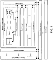
- FIG. 1 depicts an exemplary memory architecture organized into multiple memory channels, each memory channel including multiple bank groups, and each bank group including multiple SRAM banks in accordance with an embodiment of the invention.
- channel steering logic may be used to interface with L memory channels (Memory Channel 0, Memory Channel 1, Memory Channel 2, ..., Memory Channel L-2, and Memory Channel L-1), and the channel steering logic may interface with the core logic of the integrated circuit (such as the programmable fabric of an FPGA).
- L memory channels Memory Channel 0, Memory Channel 1, Memory Channel 2, ..., Memory Channel L-2, and Memory Channel L-1
- the channel steering logic may interface with the core logic of the integrated circuit (such as the programmable fabric of an FPGA).
- the channel steering logic operates to steer the accesses (read/write command and read/write data) to and from the respective memory channels from multiple inputs from the core logic. There may be multiple memory channel access ports from the core logic, and, in that case, the channel steering logic steers access from a particular access port to a correct memory channel.
- the channel steering logic can be replaced with a UIB-lite (which is a simplified version of the Universal Interface Bus).
- each memory channel includes M bank groups (Bank Group 0, Bank Group 1, Bank Group 2, ..., Bank Group M-2, and Bank Group M-1).
- each bank group includes N SRAM banks (Bank 0, Bank 1, Bank 2, ..., Bank N-2, and Bank N-1), a Port emulation circuit module, and Channel Logic.
- Bank N-1 may be a parity bank in an exemplary implementation of the bank group.
- Each bank group uses the channel logic to interface with the channel steering logic.
- the channel logic uses decodes the read/write commands to the respective bank groups and uses Port A and Port B, as provided by the port emulation circuit module, to interface with each bank group in the memory channel.
- Port A is a group read/write port
- Port B is a group read port.
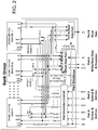
- the bank group may be formed using a number N of 1R+1W SRAM banks (Bank 0, Bank 1, ..., Bank N-2, Bank N-1) and a Port emulation circuit module.
- Each 1R+1W SRAM bank has one read port (B) and one write port (A). More particularly, each SRAM bank n has control (MEA/MEB) port, address A (ADRA) port, address B (ADRB) port, data read (QB) port, and data write (QA) port.
- ADRA address A
- ADRB address B
- QB data read
- QA data write
- the Port emulation circuit module includes a Port Emulation Control circuit, Port A Write & Read Data Path circuit, and Port B Read Data Path circuit.
- the Port Emulation Control circuit has initialization (INIT) and request command (CMD) control signal inputs, Port A Control and Address (MEA and ADRA) inputs, Port B Control and Address (MEB and ADRB) inputs.
- the Port Emulation Control circuit uses these inputs to generate various control and address signals.
- atomic operation may refer to an operation that is performed in parallel or concurrently with other operations to the same memory locations. Many systems avoid requests for atomic operations due to the possible creation of erroneous data.
- the request command (CMD) of the 1RW port (Port A) includes encodings for desired atomic operations that are mapped to either read accesses (for operations requiring only memory reads) or write accesses (for operations requiring read-modify-write sequences).
- Example encodings include: binary addition; Boolean operations (AND, NAND, NOR, OR, XOR); data swap; and arithmetic compare (equal, greater than, less than).
- the Port Emulation Control circuit generates N MEA/MEB control signals (MEA[0]/MEB[0], MEA[1]/MEB[1], MEA[2]/MEB[2], ..., MEA[N-1]/MEB[N-2], MEA[N-1]/MEB[N-1]).
- the MEA[0]/MEB[0] control is provided to SRAM Bank 0.
- the MEA[1]/MEB[1] control is provided to SRAM Bank 1.
- the MEA[2]/MEB[2] control is provided to SRAM Bank 2. And so on.
- the Port Emulation Control circuit also generates Write Address A (ADRA WRITE ), Read Address A (ADRA READ ), and Read Address B (ADRB READ ), and N selection (ASEL[0], ASEL[1], ..., ASEL[N-2], ASEL[N-1]) signals.
- the ADRA READ and ADRB READ signals provided as inputs to N selectors (S[0], S[1], ..., S[N-2], S[N-1]).
- Selector S[0] is controlled by ASEL[0].
- Selector S[1] is controlled by ASEL[1].
- Selector S[2] is controlled by ASEL[2]. And so on.
- selector S[n] When ASEL[n] is 0, then selector S[n] outputs ADRA READ to the ADRB input of SRAM Bank n. On the other hand, when ASEL[n] is 1, then selector S[n] outputs ADRB READ to the ADRB input of SRAM Bank n.
- the Port A Write & Read Data Path circuit receives the N read data outputs (QB 0 , QB 1 , ..., QB N-2 , QB N-1 ) from the N SRAM banks and the data write (DA) signal from the channel logic.
- the Port A Write & Read Data Path circuit also receives the CMR_R, RDA_EN[N-1:0], RFW_EN, and RDA_FWD_EN control signals from the Port Emulation Control circuit. Note that the CMR_R control signal conveys regular and atomic commands based on request command encodings.
- the Port A Write & Read Data Path circuit uses the various input signals to generate a first data write (DA RAW ) signal and a second data write signal (DA N-1 ).
- the first data write (DA RAW ) signal is output to the QA ports of SRAM banks 0 to N-2 and to the Port B Read Data Path circuit, and the second data write signal (DA N-1 ) is output to the QA port of SRAM bank N-1.
- the Port A Write & Read Data Path circuit also generates the response interface (RESP) signal and the data read (QA) signal that are output to the channel logic.
- RESP response interface
- the Port A Write & Read Data Path circuit includes hardware circuits for desired atomic operations between the read and the write data for the parity calculations of the write sequence. For operations taking multiple pipelined stages, hardware circuits may be pipelined as needed for timing closure.
- the response interface (RESP) signal output from the Port A Write & Read Data Path circuit may convey results of atomic operations to the channel logic.
- the RESP signal may provide the result of an arithmetic compare operation (i.e. equal, greater than, or less than).
- the Port B Read Data Path circuit receives the N data read signals (QB 0 , QB 1 , ..., QB N-2 , QB N-1 ) from the data read (QB) ports of the N SRAM banks.
- the Port B Read Data Path circuit also receives the first data write (DA RAW ) signal from the Port A Write & Read Data Path circuit. Using the various input signals, the Port B Read Data Path circuit selects the data read (QB) signal to the channel logic.
- FIG. 3 is an exemplary timing diagram for the signals of the bank group depicted in FIG. 2 in accordance with an embodiment of the invention.
- the CLK signal shows clock cycles labeled 0 to 7.
- the signals between the bank group and the channel logic include the MEA, WEA, ADRA, DA, QA, MEB, ADRB and QB signals.
- the signals internal to the bank group include the MEA[4:0], MEB[4:0], ASEL[4:0], ADRA WRITE , ADRA READ , ADRB READ , RDA_EN[4:0], RFW_EN, RDA_FWD_EN, DA RAW , DA N-1 , RDB_EN[4:0], and RDB_FWD_EN signals.
- the MEA and MEB signals transition to logical 1
- the write enable for Port A (WEA) signal is logical zero (indicating a read operation)
- read address A0_BK1 (indicating address A0 in bank 1) is received on ADRA
- read address B0_BK0 (indicating address B0 in bank 0) is received on ADRB.
- the data read QA signal outputs data QA0_BK1 (indicating the data read from address A0 in bank 1)
- the data read QB signal outputs data QB0_BK0 (indicating the data read from address B0 in bank 0).
- read address A1_BK0 (indicating address A1 in bank 0) is received on ADRA
- read address B1_BK0 (indicating address B1 in bank 0) is received on ADRB.
- the data read QA signal outputs data QA1_BK0 (indicating the data read from address A1 in bank 0).
- the data read QB signal outputs data QB1_BK0 (indicating the data read from address B1 in bank 0).
- data QA1_BK0 output in clock cycle 3 cannot be directly read from bank 0. This is because there is an access conflict at bank 0 due to both read addresses being in bank 0.
- the write enable for port A goes to logical one to indicate a write operation
- write data DA2_BK0 is received on the DA port
- write address A2_BK0 (indicating address A2 in bank 0) is received on ADRA
- read address B2_BK3 (indicating address B2 in bank 3) is received on ADRB.
- the data read QB signal outputs data QB2_BK3 (indicating the data read from address B2 in bank 3).
- write data DA3_BK2 is received on the DA port
- write address A3_BK2 (indicating address A3 in bank 2) is received on ADRA
- read address B3_BK2 (indicating address B3 in bank 2) is received on ADRB.
- the data read QB signal outputs data QB3_BK2 (indicating the data read from address B3 in bank 2).
- the write enable for port A goes to logical zero to indicate a read operation
- read address A4_BK1 (indicating address A4 in bank 1) is received on ADRA
- read address B4_BK1 (indicating address B4 in bank 1) is received on ADRB.
- the data read QA signal outputs data QA4_BK1 (indicating the data read from address A4 in bank 1)
- the data read QB signal outputs data QB4_BK1 (indicating the data read from address B4 in bank 1).
- data QA4_BK1 output in clock cycle 6 cannot be directly read from bank 1. This is because there is an access conflict at bank 1 due to both read addresses being in bank 1.
- the MEA and MEB signals go to logical zero at clock cycle 6. As such, no read or write requests are received during that clock cycle.
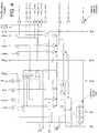
- FIG. 4 depicts detail of an exemplary port emulation control circuit in accordance with an embodiment of the invention.
- the Port Emulation Control circuit has initialization (INIT) and command (CMD) inputs, Port A Control and Address (MEA and ADRA) inputs, Port B Control and Address (MEB and ADRB) inputs.
- IIT initialization
- CMD command
- MEA and ADRA Port A Control and Address
- MEB and ADRB Port B Control and Address
- the INIT input is used to initialize the SRAM array with known content (for example, all zeroes).
- known content for example, all zeroes.
- the user logic cycles through all the address bits from port A to write all the contents in all the banks to zeroes. In an exemplary implementation, such initialization to all zeroes is required before using the smart memory.
- the Port Emulation Control circuit generates various control and address signals.
- the Port Emulation Control circuit generates N MEA/MEB control signals (MEA[0]/MEB[0], MEA[1]/MEB[1], MEA[2]/MEB[2], ..., MEA[N-1]/MEB[N-2], MEA[N-1]/MEB[N-1]).
- the Port Emulation Control circuit also generates Write Address A (ADRA WRITE ), Read Address A (ADRA READ ), and Read Address B (ADRB READ ), and N selection (ASEL[0], ASEL[1], ..., ASEL[N-2], ASEL[N-1]) signals.
- the Port Emulation Control circuit generates the control CMR_R, RDA_EN[N-1:0], RFW_EN, and RDA_FWD_EN control signals.
- a first configuration bit is the Data Reconstruction Enable bit.
- the Data Reconstruction Enable bit When the Data Reconstruction Enable bit is logical one, then read reconstruction is enabled. When the Data Reconstruction Enable bit is logical zero, then read reconstruction is disabled.
- the Data Reconstruction Enable allows reconstruction of the contents of an entire bank by reusing the same port emulation mechanism. For example, if multiple bits in bank 0 are corrupted due to a single event upset (SEU) or other errors, then the user logic may enable data reconstruction and do a read and write back to the bank 0 from port A. This causes the data to be reconstructed from banks 1, 2, ..., N-1 (not read from bank 0) and then written back to bank 0. This corrects the errors in bank 0.
- SEU single event upset
- a second configuration bit is the Port A Read Enable bit. When the Port A Read Enable bit is logical one, then the Port A read operation is enabled. When the Port A Read Enable bit is logical zero, then the Port A read operation is disabled.
- the Port Emulation Control circuit includes a command decode path.
- the command decode path operates to decode atomic operations.
- a pipelined command (CMD_R) is provided to the Port A Write & Read Data Path circuit.
- the pipelined command may be used to identify the atomic operation to be performed by the Port A Write & Read Data Path circuit on one or more operands.
- the operands may include Operand 1 that may be obtained, or reconstructed from, QB 0 to QB N-1 and optional Operand 2 that may be provided by DA.
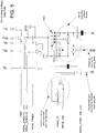
- FIG. 5 depicts detail of a port A write and read data path circuit in accordance with an embodiment of the invention.
- the Port A Write & Read Data Path circuit receives the N read data outputs (QB 0 , QB 1 , ..., QB N-2 , QB N-1 ) from the N SRAM banks and the data write (DA) signal from the channel logic.
- the Port A Write & Read Data Path circuit also receives the CMR_R, RDA_EN[N-1:0], RFW_EN, and RDA_FWD_EN control signals from the Port Emulation Control circuit.
- the Port A Write & Read Data Path circuit uses the various input signals to generate a first data write (DA RAW ) signal and a second data write signal (DA N-1 ).
- the Port A Write & Read Data Path circuit also generates the response (RESP) signal and the data read (QA) signal that are output to the channel logic.
- RESP response
- QA data read
- atomic operation hardware circuitry may be included in the port A write and read data path circuit.
- the atomic operation hardware circuitry may include binary adder logic (ADD), Boolean operation logic (BOOL) (such as AND, NAND, OR, NOR, and XOR logic), and compare logic (CMP).
- control circuitry may be included to allow read data return for a data swap operation (SWAP).
- a multiplexer (MUX) may be used to select the write data to be written back (modified or raw write data) and used for a final parity calculation.
- the original read data may be returned via the emulated read data path (QA), and the Response interface (RESP) may be used to convey the result of the arithmetic compare operation performed by the compare logic (CMP).
- FIG. 6 is a flow chart of a method 600 for a data read of an entry within a conflicting bank from the 1RW port of a bank group in accordance with an embodiment of the invention.
- the method 600 may be implemented using the exemplary circuits described above in relation to FIGS. 1-5 .
- a data read command is received from the 1RW port of the bank group.
- Port A is the 1RW port of the bank group, and the data read command is received at the 1RW port by having MEA enabled and WEA disabled and receiving the read address and bank number in ADRA.
- Per step 604 it is determined that the data read is to a bank that has a conflicting data read from the 1R port of the bank group.
- Port B is the 1R port of the bank group, and a data read command is received at the 1R port by having MEB enabled and receiving the read address and bank number in ADRB. Examples of conflicting data reads from the 1RW and 1R ports are discussed above in relation to the timing diagram of FIG 3 . Note that, if there is no conflict at the bank, then the data read may proceed directly, without reconstruction, as discussed above in relation to the timing diagram of FIG 3 .
- Per step 608, the data to fulfill the data read from the 1RW port is reconstructed.
- the corresponding bit in bank 3 may be reconstructed as a logical 1.
- the corresponding bits in banks 0, 1, 2 and 4 add up to an even number, then the corresponding bit in bank 3 may be reconstructed as a logical 0. In this way, the data to fulfill the data read from the 1RW port may be reconstructed bit by bit.
- the reconstructed data is output via the 1RW port of the bank group.
- Port A is the 1RW port of the bank group, and the reconstructed data is output from the 1RW port in the data QA.
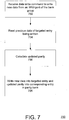
- FIG. 7 is a flow chart of a method 700 for a data write to an entry in a bank from the emulated 1RW port of a bank group in accordance with an embodiment of the invention.
- the method 700 may be implemented using the exemplary circuits described above in relation to FIGS. 1-5 .
- a data write command is received from the 1RW port of the bank group.
- Port A is the 1RW port of the bank group, and the data write command is received at the 1RW port by having MEA and WEA both enabled and receiving the write address and bank number in ADRA.
- the previous data stored at the targeted entry being written (i.e. the data at the write address and bank number received in ADRA) is read.
- the previous data may be read directly if there is no read bank conflict, or the previous data may be reconstructed if there is a read bank conflict.
- the updated parity data (for the write address in the parity bank) is calculated. As indicated in the timing diagram of FIG. 3 , the updated parity data is output to the DA N-1 data signal.
- the new data is written into the targeted entry, and the updated parity data is written into the parity bank.
- the DA RAW data signal provides the new data that is written into the bank indicated by MEA[N-2:0].
- the DA N-1 signal provides the updated parity data that is written into bank N-1 at the address indicated by ADRA WRITE .
- the write sequence described above in relation to FIG. 7 is a type of read-modify-write (RMW) sequence.
- the "modification" step of the RMW sequence is the operation of calculating the new parity value to be written into the parity bank.
- FIG. 8 is a simplified partial block diagram of a field programmable gate array (FPGA) 10 that can include aspects of the present invention. It should be understood that embodiments of the present invention can be used in numerous types of integrated circuits such as field programmable gate arrays (FPGAs), programmable logic devices (PLDs), complex programmable logic devices (CPLDs), programmable logic arrays (PLAs), digital signal processors (DSPs) and application specific integrated circuits (ASICs).
- FPGAs field programmable gate arrays
- PLDs programmable logic devices
- CPLDs complex programmable logic devices
- PLAs programmable logic arrays
- DSPs digital signal processors
- ASICs application specific integrated circuits
- FPGA 10 includes within its "core" a two-dimensional array of programmable logic array blocks (or LABs) 12 that are interconnected by a network of column and row interconnect conductors of varying length and speed.
- LABs 12 include multiple (e.g., ten) logic elements (or LEs).
- An LE is a programmable logic block that provides for efficient implementation of user defined logic functions.
- An FPGA has numerous logic elements that can be configured to implement various combinatorial and sequential functions.
- the logic elements have access to a programmable interconnect structure.
- the programmable interconnect structure can be programmed to interconnect the logic elements in almost any desired configuration.
- FPGA 10 may also include a distributed memory structure including random access memory (RAM) blocks of varying sizes provided throughout the array.
- RAM random access memory
- the RAM blocks include, for example, blocks 14 , blocks 16 , and block 18 .
- These memory blocks can also include shift registers and FIFO buffers.
- FPGA 10 may further include digital signal processing (DSP) blocks 20 that can implement, for example, multipliers with add or subtract features.
- DSP digital signal processing
- IOEs 22 located, in this example, around the periphery of the chip support numerous single-ended and differential input/output standards. Each IOE 22 is coupled to an external terminal (i.e., a pin) of FPGA 10 .
- a transceiver (TX/RX) channel array may be arranged as shown, for example, with each TX/RX channel circuit 30 being coupled to several LABs.
- FPGA 10 is described herein for illustrative purposes only and that the present invention can be implemented in many different types of PLDs, FPGAs, and ASICs.
- FIG. 9 shows a block diagram of an exemplary digital system 50 that can embody techniques of the present invention.
- System 50 may be a programmed digital computer system, digital signal processing system, specialized digital switching network, or other processing system. Moreover, such systems can be designed for a wide variety of applications such as telecommunications systems, automotive systems, control systems, consumer electronics, personal computers, Internet communications and networking, and others. Further, system 50 may be provided on a single board, on multiple boards, or within multiple enclosures.
- System 50 includes a processing unit 52 , a memory unit 54 , and an input/output (I/O) unit 56 interconnected together by one or more buses.
- FPGA 58 is embedded in processing unit 52 .
- FPGA 58 can serve many different purposes within the system 50 .
- FPGA 58 can, for example, be a logical building block of processing unit 52 , supporting its internal and external operations.
- FPGA 58 is programmed to implement the logical functions necessary to carry on its particular role in system operation.
- FPGA 58 can be specially coupled to memory 54 through connection 60 and to I/O unit 56 through connection 62 .
- Processing unit 52 may direct data to an appropriate system component for processing or storage, execute a program stored in memory 54 , receive and transmit data via I/O unit 56 , or other similar function.
- Processing unit 52 may be a central processing unit (CPU), microprocessor, floating point coprocessor, graphics coprocessor, hardware controller, microcontroller, field programmable gate array programmed for use as a controller, network controller, or any type of processor or controller. Furthermore, in many embodiments, there is often no need for a CPU.
- FPGA 58 may control the logical operations of the system.
- FPGA 58 acts as a reconfigurable processor that may be reprogrammed as needed to handle a particular computing task.
- FPGA 58 may itself include an embedded microprocessor.
- Memory unit 54 may be a random access memory (RAM), read only memory (ROM), fixed or flexible disk media, flash memory, tape, or any other storage means, or any combination of these storage means.
Landscapes
- Engineering & Computer Science (AREA)
- Theoretical Computer Science (AREA)
- General Physics & Mathematics (AREA)
- Physics & Mathematics (AREA)
- General Engineering & Computer Science (AREA)
- Human Computer Interaction (AREA)
- Microelectronics & Electronic Packaging (AREA)
- Multimedia (AREA)
- Quality & Reliability (AREA)
- Computer Security & Cryptography (AREA)
- Computer Hardware Design (AREA)
- Techniques For Improving Reliability Of Storages (AREA)
- Static Random-Access Memory (AREA)
Abstract
Description
- This application claims priority to United States Patent Application No.
15/193,686, filed on June 27, 2016 - The present disclosure relates generally to the technology area of interface architectures for communicating with memory devices.
- Static random access memory (SRAM) is commonly used in integrated circuits. SRAM cells have the advantageous feature of holding data without a need for refreshing. SRAM cells may include different numbers of transistors, and are often accordingly referred to by the number of transistors, for example, six-transistor (6T) SRAM, eight-transistor (8T) SRAM, and the like. The transistors typically form a data latch for storing a bit. Additional transistors may be added to control the access to the transistors. SRAM cells are typically arranged as an array having rows and columns. Typically, each row of the SRAM cells is connected to a word-line, which determines whether the current SRAM cell is selected or not. Each column of the SRAM cells is connected to a bit-line, which is used for storing a bit into the SRAM cell or read from the SRAM cell.
- One embodiment relates to a memory structure that includes a bank group and a port emulation circuit module. The bank group includes a plurality of memory banks, each memory bank having one read port and one write port. The port emulation circuit module provides a group read/write port and a group read port for the bank group.
- Another embodiment relates to a port emulation circuit module. The port emulation circuit module includes a port emulation control circuit that receives control signals including a first address for a group read/write port and a second address for a group read port, a first data path circuit for the group read/write port, and a second data path circuit for the group read port, wherein the second data path circuit outputs a second read data.
- Another embodiment relates to a method of reading data from a memory bank group. A data read requesting data at a read address in a specified memory bank is received from a read/write port of the memory bank group. A determination is made that the specified memory bank has a conflicting data read from a read port of the memory bank group. Data is read from the read address in all other memory banks in the memory bank group. The data at the read address in the specified memory bank is reconstructed using the data read from the read address in all the other memory banks.
- Another embodiment relates to a method of writing data to a memory bank group. A data write is received that requests new data be written to a write address in a specified memory bank of the memory bank group. Previous data at the write address in the specified memory bank is read. An updated parity is calculated, and the updated parity is written to the write address in a parity memory bank of the memory bank group. The new data is written to the write address in the specified memory bank.
- Other embodiments and features are also disclosed.
-
-
FIG. 1 depicts an exemplary memory architecture organized into multiple memory channels, each memory channel including multiple bank groups, and each bank group including multiple SRAM banks in accordance with an embodiment of the invention. -
FIG. 2 depicts further detail of an exemplary bank group in accordance with an embodiment of the invention. -
FIG. 3 is an exemplary timing diagram for the signals of the bank group depicted inFIG. 2 in accordance with an embodiment of the invention. -
FIG. 4 depicts detail of an exemplary port emulation control circuit in accordance with an embodiment of the invention. -
FIG. 5 depicts detail of a port A write and read data path circuit in accordance with an embodiment of the invention. -
FIG. 6 is a flow chart of a method for a data read of an entry within a conflicting bank from the emulated 1RW port in accordance with an embodiment of the invention. -
FIG. 7 is a flow chart of a method for a data write to an entry in a bank from the emulated 1RW port in accordance with an embodiment of the invention. -
FIG. 8 is a simplified partial block diagram of a field programmable gate array (FPGA) that can include aspects of the present invention. -
FIG. 9 is a block diagram of an exemplary digital system that can employ techniques of the present invention. - The present disclosure provides circuit structures and method of operation for a smart memory interface. The smart memory interface is capable of executing smart memory functions and may provide an emulated 1R+1RW (one read port and one read/write port) SRAM channel from a collection of 1R+1W (one read port and one write port) SRAM banks without memory access restrictions. The smart memory interface may also be configured so that the collection of 1R+1W SRAM banks operates as a large 1R+1W SRAM if the emulated 1R+1RW SRAM channel is not desired. The configuration implemented may depend on the application mapped to the core logic of the integrated circuit.
- The "smartness" is provided via atomic operation functionalities to the 1RW port. The atomic operation functionalities allow for applications to perform smart memory operations on the SRAM memory itself without affecting the raw memory bandwidth and with low power.
- The smart memory interface may advantageously reduce application power and transaction bandwidth required for common read-modify-write operations. This is accomplished by removing the need to physically transfer the read data from the SRAM back to the core logic of the integrated circuit (such as, for example, the core fabric of a field programmable gate array) for modifications and transferring the write data back to be written to the same SRAM location.
- The smart memory interface may also advantageously allow the swapping of temporal data storage contents for store-and-forward memory applications. This reduces memory capacity, power and bandwidth requirements for the applications.
-
FIG. 1 depicts an exemplary memory architecture organized into multiple memory channels, each memory channel including multiple bank groups, and each bank group including multiple SRAM banks in accordance with an embodiment of the invention. As depicted, channel steering logic may be used to interface with L memory channels (Memory Channel 0,Memory Channel 1,Memory Channel 2, ..., Memory Channel L-2, and Memory Channel L-1), and the channel steering logic may interface with the core logic of the integrated circuit (such as the programmable fabric of an FPGA). - The channel steering logic operates to steer the accesses (read/write command and read/write data) to and from the respective memory channels from multiple inputs from the core logic. There may be multiple memory channel access ports from the core logic, and, in that case, the channel steering logic steers access from a particular access port to a correct memory channel. In some embodiments, the channel steering logic can be replaced with a UIB-lite (which is a simplified version of the Universal Interface Bus).
- An expanded view is shown for the internal structure of
Memory Channel 0, and the same internal structure would also be present in the other L-1 memory channels. As shown, each memory channel includes M bank groups (Bank Group 0, Bank Group 1, Bank Group 2, ..., Bank Group M-2, and Bank Group M-1). - An expanded view is shown for the internal structure of
Bank Group 0, and the same internal structure would also be present in the other M-1 bank groups. As shown, each bank group includes N SRAM banks (Bank 0,Bank 1,Bank 2, ..., Bank N-2, and Bank N-1), a Port emulation circuit module, and Channel Logic. As indicated, Bank N-1 may be a parity bank in an exemplary implementation of the bank group. Each bank group uses the channel logic to interface with the channel steering logic. The channel logic uses decodes the read/write commands to the respective bank groups and uses Port A and Port B, as provided by the port emulation circuit module, to interface with each bank group in the memory channel. Port A is a group read/write port, and Port B is a group read port.FIG. 2 depicts further detail of an exemplary bank group in accordance with an embodiment of the invention. As depicted, the bank group may be formed using a number N of 1R+1W SRAM banks (Bank 0,Bank 1, ..., Bank N-2, Bank N-1) and a Port emulation circuit module. - One of the 1R+1W SRAM banks in the bank group is a parity bank. In an exemplary implementation, Bank N-1 is the parity bank. Each 1R+1W SRAM bank has one read port (B) and one write port (A). More particularly, each SRAM bank n has control (MEA/MEB) port, address A (ADRA) port, address B (ADRB) port, data read (QB) port, and data write (QA) port.
- The Port emulation circuit module includes a Port Emulation Control circuit, Port A Write & Read Data Path circuit, and Port B Read Data Path circuit.
- The Port Emulation Control circuit has initialization (INIT) and request command (CMD) control signal inputs, Port A Control and Address (MEA and ADRA) inputs, Port B Control and Address (MEB and ADRB) inputs. The Port Emulation Control circuit uses these inputs to generate various control and address signals.
- Note that the term "atomic" operation may refer to an operation that is performed in parallel or concurrently with other operations to the same memory locations. Many systems avoid requests for atomic operations due to the possible creation of erroneous data.
- In an exemplary implementation, the request command (CMD) of the 1RW port (Port A) includes encodings for desired atomic operations that are mapped to either read accesses (for operations requiring only memory reads) or write accesses (for operations requiring read-modify-write sequences). Example encodings include: binary addition; Boolean operations (AND, NAND, NOR, OR, XOR); data swap; and arithmetic compare (equal, greater than, less than).
- The Port Emulation Control circuit generates N MEA/MEB control signals (MEA[0]/MEB[0], MEA[1]/MEB[1], MEA[2]/MEB[2], ..., MEA[N-1]/MEB[N-2], MEA[N-1]/MEB[N-1]). The MEA[0]/MEB[0] control is provided to
SRAM Bank 0. The MEA[1]/MEB[1] control is provided toSRAM Bank 1. The MEA[2]/MEB[2] control is provided toSRAM Bank 2. And so on. - The Port Emulation Control circuit also generates Write Address A (ADRAWRITE), Read Address A (ADRAREAD), and Read Address B (ADRBREAD), and N selection (ASEL[0], ASEL[1], ..., ASEL[N-2], ASEL[N-1]) signals. The ADRAREAD and ADRBREAD signals provided as inputs to N selectors (S[0], S[1], ..., S[N-2], S[N-1]). Selector S[0] is controlled by ASEL[0]. Selector S[1] is controlled by ASEL[1]. Selector S[2] is controlled by ASEL[2]. And so on. When ASEL[n] is 0, then selector S[n] outputs ADRAREAD to the ADRB input of SRAM Bank n. On the other hand, when ASEL[n] is 1, then selector S[n] outputs ADRBREAD to the ADRB input of SRAM Bank n.
- The Port A Write & Read Data Path circuit receives the N read data outputs (QB0, QB1, ..., QBN-2, QBN-1) from the N SRAM banks and the data write (DA) signal from the channel logic. The Port A Write & Read Data Path circuit also receives the CMR_R, RDA_EN[N-1:0], RFW_EN, and RDA_FWD_EN control signals from the Port Emulation Control circuit. Note that the CMR_R control signal conveys regular and atomic commands based on request command encodings.
- Using the various input signals, the Port A Write & Read Data Path circuit generates a first data write (DARAW) signal and a second data write signal (DAN-1). The first data write (DARAW) signal is output to the QA ports of
SRAM banks 0 to N-2 and to the Port B Read Data Path circuit, and the second data write signal (DAN-1) is output to the QA port of SRAM bank N-1. The Port A Write & Read Data Path circuit also generates the response interface (RESP) signal and the data read (QA) signal that are output to the channel logic. - Note that, in an exemplary implementation, the Port A Write & Read Data Path circuit includes hardware circuits for desired atomic operations between the read and the write data for the parity calculations of the write sequence. For operations taking multiple pipelined stages, hardware circuits may be pipelined as needed for timing closure.
- Note further that, in an exemplary implementation, the response interface (RESP) signal output from the Port A Write & Read Data Path circuit may convey results of atomic operations to the channel logic. For example, the RESP signal may provide the result of an arithmetic compare operation (i.e. equal, greater than, or less than).
- The Port B Read Data Path circuit receives the N data read signals (QB0, QB1, ..., QBN-2, QBN-1) from the data read (QB) ports of the N SRAM banks. The Port B Read Data Path circuit also receives the first data write (DARAW) signal from the Port A Write & Read Data Path circuit. Using the various input signals, the Port B Read Data Path circuit selects the data read (QB) signal to the channel logic.
-
FIG. 3 is an exemplary timing diagram for the signals of the bank group depicted inFIG. 2 in accordance with an embodiment of the invention. The timing diagram assumes that N=5, such that there are five SRAM banks in the bank group. - The CLK signal shows clock cycles labeled 0 to 7. The signals between the bank group and the channel logic include the MEA, WEA, ADRA, DA, QA, MEB, ADRB and QB signals. The signals internal to the bank group include the MEA[4:0], MEB[4:0], ASEL[4:0], ADRAWRITE, ADRAREAD, ADRBREAD, RDA_EN[4:0], RFW_EN, RDA_FWD_EN, DARAW, DAN-1, RDB_EN[4:0], and RDB_FWD_EN signals.
- In the example shown, at
clock cycle 1, the MEA and MEB signals transition to logical 1, the write enable for Port A (WEA) signal is logical zero (indicating a read operation), read address A0_BK1 (indicating address A0 in bank 1) is received on ADRA, and read address B0_BK0 (indicating address B0 in bank 0) is received on ADRB. Atclock cycle 2, in fulfillment of the read requests of the previous clock cycle, the data read QA signal outputs data QA0_BK1 (indicating the data read from address A0 in bank 1), and the data read QB signal outputs data QB0_BK0 (indicating the data read from address B0 in bank 0). - Similarly, at
clock cycle 2, read address A1_BK0 (indicating address A1 in bank 0) is received on ADRA, and read address B1_BK0 (indicating address B1 in bank 0) is received on ADRB. Atclock cycle 3, in fulfillment of the read requests of the previous clock cycle, the data read QA signal outputs data QA1_BK0 (indicating the data read from address A1 in bank 0). In addition, due to ASEL[4:0] being set to logical one, the data read QB signal outputs data QB1_BK0 (indicating the data read from address B1 in bank 0). - Note that data QA1_BK0 output in
clock cycle 3 cannot be directly read frombank 0. This is because there is an access conflict atbank 0 due to both read addresses being inbank 0. Hence, in accordance with an embodiment of the present disclosure, the data QA1_BK0 is reconstructed using themethod 600 described below in relation toFIG. 6 . In this case, the reconstruction requires data frombanks 1 to 4 (but not bank 0), so RDA_EN[4:0] = 11110 inclock cycle 3. - At
clock cycle 3, the write enable for port A (WEA) goes to logical one to indicate a write operation, write data DA2_BK0 is received on the DA port, write address A2_BK0 (indicating address A2 in bank 0) is received on ADRA, and read address B2_BK3 (indicating address B2 in bank 3) is received on ADRB. Atclock cycle 4, as a consequence of the write command on port A in the previous cycle, the previous data of the targeted entry is read directly from address A2 inbank 0, and the clock parity for address A2 inbank 4 is updated (so RDA_EN[4:0] = 10001, ADAWRITE=A2, and DAN-1= DA4=DA2(P) in clock cycle 4). In addition, in fulfillment of the read command on port B in the previous clock cycle, the data read QB signal outputs data QB2_BK3 (indicating the data read from address B2 in bank 3). - At
clock cycle 4, write data DA3_BK2 is received on the DA port, write address A3_BK2 (indicating address A3 in bank 2) is received on ADRA, and read address B3_BK2 (indicating address B3 in bank 2) is received on ADRB. Atclock cycle 5, as a consequence of the write command on port A in the previous cycle, the previous data of the targeted entry is reconstructed (due to the read conflict at bank 2) for address A3 inbank 2, and the clock parity for address A3 inbank 4 is updated (so RDA_EN[4:0] = 11011, ADAWRITE=A3, and DAN-1= DA4=DA3(P) in clock cycle 5). In addition, in fulfillment of the read request of the previous clock cycle, the data read QB signal outputs data QB3_BK2 (indicating the data read from address B3 in bank 2). - At
clock cycle 5, the write enable for port A (WEA) goes to logical zero to indicate a read operation, read address A4_BK1 (indicating address A4 in bank 1) is received on ADRA, and read address B4_BK1 (indicating address B4 in bank 1) is received on ADRB. Atclock cycle 6, in fulfillment of the read requests of the previous clock cycle, the data read QA signal outputs data QA4_BK1 (indicating the data read from address A4 in bank 1), and the data read QB signal outputs data QB4_BK1 (indicating the data read from address B4 in bank 1). - Note that data QA4_BK1 output in
clock cycle 6 cannot be directly read frombank 1. This is because there is an access conflict atbank 1 due to both read addresses being inbank 1. Hence, in accordance with an embodiment of the present disclosure, the data QA4_BK1 is reconstructed using themethod 600 described below in relation toFIG. 6 . In this case, the reconstruction requires data frombanks clock cycle 6. - Also the MEA and MEB signals go to logical zero at
clock cycle 6. As such, no read or write requests are received during that clock cycle. -
FIG. 4 depicts detail of an exemplary port emulation control circuit in accordance with an embodiment of the invention. As depicted, the Port Emulation Control circuit has initialization (INIT) and command (CMD) inputs, Port A Control and Address (MEA and ADRA) inputs, Port B Control and Address (MEB and ADRB) inputs. - The INIT input is used to initialize the SRAM array with known content (for example, all zeroes). When INIT is asserted, the user logic cycles through all the address bits from port A to write all the contents in all the banks to zeroes. In an exemplary implementation, such initialization to all zeroes is required before using the smart memory.
- The Port Emulation Control circuit generates various control and address signals. In particular, the Port Emulation Control circuit generates N MEA/MEB control signals (MEA[0]/MEB[0], MEA[1]/MEB[1], MEA[2]/MEB[2], ..., MEA[N-1]/MEB[N-2], MEA[N-1]/MEB[N-1]). The Port Emulation Control circuit also generates Write Address A (ADRAWRITE), Read Address A (ADRAREAD), and Read Address B (ADRBREAD), and N selection (ASEL[0], ASEL[1], ..., ASEL[N-2], ASEL[N-1]) signals. Finally, the Port Emulation Control circuit generates the control CMR_R, RDA_EN[N-1:0], RFW_EN, and RDA_FWD_EN control signals.
- Two configuration bits are shown for the Port Emulation Control circuit. A first configuration bit is the Data Reconstruction Enable bit. When the Data Reconstruction Enable bit is logical one, then read reconstruction is enabled. When the Data Reconstruction Enable bit is logical zero, then read reconstruction is disabled. In an exemplary implementation, the Data Reconstruction Enable allows reconstruction of the contents of an entire bank by reusing the same port emulation mechanism. For example, if multiple bits in
bank 0 are corrupted due to a single event upset (SEU) or other errors, then the user logic may enable data reconstruction and do a read and write back to thebank 0 from port A. This causes the data to be reconstructed frombanks bank 0. This corrects the errors inbank 0. - A second configuration bit is the Port A Read Enable bit. When the Port A Read Enable bit is logical one, then the Port A read operation is enabled. When the Port A Read Enable bit is logical zero, then the Port A read operation is disabled.
- Note that, as shown in
FIG. 4 , the Port Emulation Control circuit includes a command decode path. The command decode path operates to decode atomic operations. In addition, a pipelined command (CMD_R) is provided to the Port A Write & Read Data Path circuit. The pipelined command may be used to identify the atomic operation to be performed by the Port A Write & Read Data Path circuit on one or more operands. In particular, the operands may includeOperand 1 that may be obtained, or reconstructed from, QB0 to QBN-1 andoptional Operand 2 that may be provided by DA. -
FIG. 5 depicts detail of a port A write and read data path circuit in accordance with an embodiment of the invention. As shown, the Port A Write & Read Data Path circuit receives the N read data outputs (QB0, QB1, ..., QBN-2,
QBN-1) from the N SRAM banks and the data write (DA) signal from the channel logic. The Port A Write & Read Data Path circuit also receives the CMR_R, RDA_EN[N-1:0], RFW_EN, and RDA_FWD_EN control signals from the Port Emulation Control circuit. - Using the various input signals, the Port A Write & Read Data Path circuit generates a first data write (DARAW) signal and a second data write signal (DAN-1). The Port A Write & Read Data Path circuit also generates the response (RESP) signal and the data read (QA) signal that are output to the channel logic.
- As shown in
FIG. 5 , atomic operation hardware circuitry may be included in the port A write and read data path circuit. The atomic operation hardware circuitry may include binary adder logic (ADD), Boolean operation logic (BOOL) (such as AND, NAND, OR, NOR, and XOR logic), and compare logic (CMP). In addition, control circuitry may be included to allow read data return for a data swap operation (SWAP). A multiplexer (MUX) may be used to select the write data to be written back (modified or raw write data) and used for a final parity calculation. The original read data may be returned via the emulated read data path (QA), and the Response interface (RESP) may be used to convey the result of the arithmetic compare operation performed by the compare logic (CMP). -
FIG. 6 is a flow chart of amethod 600 for a data read of an entry within a conflicting bank from the 1RW port of a bank group in accordance with an embodiment of the invention. Themethod 600 may be implemented using the exemplary circuits described above in relation toFIGS. 1-5 . - Per
step 602, a data read command is received from the 1RW port of the bank group. In the exemplary circuits described above, Port A is the 1RW port of the bank group, and the data read command is received at the 1RW port by having MEA enabled and WEA disabled and receiving the read address and bank number in ADRA. - Per
step 604, it is determined that the data read is to a bank that has a conflicting data read from the 1R port of the bank group. In the exemplary circuits described above, Port B is the 1R port of the bank group, and a data read command is received at the 1R port by having MEB enabled and receiving the read address and bank number in ADRB. Examples of conflicting data reads from the 1RW and 1R ports are discussed above in relation to the timing diagram ofFIG 3 . Note that, if there is no conflict at the bank, then the data read may proceed directly, without reconstruction, as discussed above in relation to the timing diagram ofFIG 3 . - Per
step 606, in order to fulfill the data read from the 1RW port, data is read from the same address in all the other banks in the bank group. All the other banks include all the non-conflicting data banks and the parity bank. For example, if N=5, such that the bank numbers go from 0 to 4, and the conflicted bank number is 3, then data is read from the same address inbanks bank 4 may be the parity bank. - Per
step 608, the data to fulfill the data read from the 1RW port is reconstructed. Consider the example where N=5, the conflicted bank number is 3, and where the parity bank (bank 4) holds even parity bits. In this example, if corresponding bits inbanks bank 3 may be reconstructed as a logical 1. On the other hand, if the corresponding bits inbanks bank 3 may be reconstructed as a logical 0. In this way, the data to fulfill the data read from the 1RW port may be reconstructed bit by bit. - Per
step 610, the reconstructed data is output via the 1RW port of the bank group. In the exemplary circuits described above, Port A is the 1RW port of the bank group, and the reconstructed data is output from the 1RW port in the data QA. -
FIG. 7 is a flow chart of amethod 700 for a data write to an entry in a bank from the emulated 1RW port of a bank group in accordance with an embodiment of the invention. Themethod 700 may be implemented using the exemplary circuits described above in relation toFIGS. 1-5 . - Per
step 702, a data write command is received from the 1RW port of the bank group. In the exemplary circuits described above, Port A is the 1RW port of the bank group, and the data write command is received at the 1RW port by having MEA and WEA both enabled and receiving the write address and bank number in ADRA. - Per
step 704, the previous data stored at the targeted entry being written (i.e. the data at the write address and bank number received in ADRA) is read. As discussed above in relation to the timing diagram ofFIG. 3 , the previous data may be read directly if there is no read bank conflict, or the previous data may be reconstructed if there is a read bank conflict. - Per
step 706, the updated parity data (for the write address in the parity bank) is calculated. As indicated in the timing diagram ofFIG. 3 , the updated parity data is output to the DAN-1 data signal. - Per
step 708, the new data is written into the targeted entry, and the updated parity data is written into the parity bank. As indicated in the timing diagram ofFIG. 3 , the DARAW data signal provides the new data that is written into the bank indicated by MEA[N-2:0]. As further indicated in the timing diagram ofFIG. 3 , the DAN-1 signal provides the updated parity data that is written into bank N-1 at the address indicated by ADRAWRITE. - Note that the write sequence described above in relation to
FIG. 7 is a type of read-modify-write (RMW) sequence. The "modification" step of the RMW sequence is the operation of calculating the new parity value to be written into the parity bank. -
FIG. 8 is a simplified partial block diagram of a field programmable gate array (FPGA) 10 that can include aspects of the present invention. It should be understood that embodiments of the present invention can be used in numerous types of integrated circuits such as field programmable gate arrays (FPGAs), programmable logic devices (PLDs), complex programmable logic devices (CPLDs), programmable logic arrays (PLAs), digital signal processors (DSPs) and application specific integrated circuits (ASICs). -
FPGA 10 includes within its "core" a two-dimensional array of programmable logic array blocks (or LABs) 12 that are interconnected by a network of column and row interconnect conductors of varying length and speed.LABs 12 include multiple (e.g., ten) logic elements (or LEs). - An LE is a programmable logic block that provides for efficient implementation of user defined logic functions. An FPGA has numerous logic elements that can be configured to implement various combinatorial and sequential functions. The logic elements have access to a programmable interconnect structure. The programmable interconnect structure can be programmed to interconnect the logic elements in almost any desired configuration.
-
FPGA 10 may also include a distributed memory structure including random access memory (RAM) blocks of varying sizes provided throughout the array. The RAM blocks include, for example, blocks 14, blocks 16, and block 18. These memory blocks can also include shift registers and FIFO buffers. -
FPGA 10 may further include digital signal processing (DSP) blocks 20 that can implement, for example, multipliers with add or subtract features. Input/output elements (IOEs) 22 located, in this example, around the periphery of the chip support numerous single-ended and differential input/output standards. EachIOE 22 is coupled to an external terminal (i.e., a pin) ofFPGA 10. A transceiver (TX/RX) channel array may be arranged as shown, for example, with each TX/RX channel circuit 30 being coupled to several LABs. - It is to be understood that
FPGA 10 is described herein for illustrative purposes only and that the present invention can be implemented in many different types of PLDs, FPGAs, and ASICs. -
FIG. 9 shows a block diagram of an exemplarydigital system 50 that can embody techniques of the present invention.System 50 may be a programmed digital computer system, digital signal processing system, specialized digital switching network, or other processing system. Moreover, such systems can be designed for a wide variety of applications such as telecommunications systems, automotive systems, control systems, consumer electronics, personal computers, Internet communications and networking, and others. Further,system 50 may be provided on a single board, on multiple boards, or within multiple enclosures. -
System 50 includes aprocessing unit 52, amemory unit 54, and an input/output (I/O)unit 56 interconnected together by one or more buses. According to this exemplary embodiment,FPGA 58 is embedded inprocessing unit 52.FPGA 58 can serve many different purposes within thesystem 50.FPGA 58 can, for example, be a logical building block ofprocessing unit 52, supporting its internal and external operations.FPGA 58 is programmed to implement the logical functions necessary to carry on its particular role in system operation.FPGA 58 can be specially coupled tomemory 54 throughconnection 60 and to I/O unit 56 throughconnection 62. - Processing
unit 52 may direct data to an appropriate system component for processing or storage, execute a program stored inmemory 54, receive and transmit data via I/O unit 56, or other similar function. Processingunit 52 may be a central processing unit (CPU), microprocessor, floating point coprocessor, graphics coprocessor, hardware controller, microcontroller, field programmable gate array programmed for use as a controller, network controller, or any type of processor or controller. Furthermore, in many embodiments, there is often no need for a CPU. - For example, instead of a CPU, one or
more FPGAs 58 may control the logical operations of the system. As another example,FPGA 58 acts as a reconfigurable processor that may be reprogrammed as needed to handle a particular computing task. Alternately,FPGA 58 may itself include an embedded microprocessor.Memory unit 54 may be a random access memory (RAM), read only memory (ROM), fixed or flexible disk media, flash memory, tape, or any other storage means, or any combination of these storage means. - The following examples pertain to further embodiments.
- Example 1 is a memory structure comprising: a bank group comprising a plurality of memory banks, each memory bank having one read port and one write port; and a port emulation circuit module that provides a group read/write port and a group read port for the bank group.
- Example 2 is the memory structure of example 1, wherein the port emulation circuit module optionally comprises: a port emulation control circuit that receives control signals including a first address for the group read/write port and a second address for the group read port.
- Example 3 is the memory structure of example 1, wherein the port emulation control circuit optionally includes a command decode path circuit.
- Example 4 is the memory structure of example 3, wherein the port emulation circuit module optionally further comprises: a first data path circuit for the group read/write port, wherein the first data path circuit receives write data and outputs first read data; and a second data path circuit for the group read port, wherein the second data path circuit outputs second read data.
- Example 5 is the memory structure of example 1, wherein the first data path circuit optionally includes circuitry for atomic operations.
- Example 6 is the memory structure of example 5, wherein the circuitry for atomic operations optionally includes binary adder logic, Boolean operation logic, compare logic, and data swap logic.
- Example 7 is the memory structure of example 1, wherein the port emulation circuit module reconstructs data requested by a data read command received from the group read/write port when there is a bank conflict with a data read command received from the group read port.
- Example 8 is the memory structure of example 7, wherein the data requested by the data read command received from the group read/write port is reconstructed by reading data from a same address in all other memory banks in the bank group.
- Example 9 is the memory structure of example 1, wherein, after receiving a data write command from the group read/write port to write new data to a targeted entry, the port emulation circuit module reads previous data of the targeted entry.
- Example 10 is the memory structure of example 9, wherein, after receiving the data write command from the group read/write port to write the new data to the targeted entry, the port emulation circuit module also calculates an updated parity and writes the updated parity into a corresponding entry in a parity bank of the bank group.
- Example 11 is a port emulation circuit module, the circuit module comprising: a port emulation control circuit that receives control signals including a first address for a group read/write port and a second address for a group read port; a first data path circuit for the group read/write port, wherein the first data path circuit receives write data and outputs first read data; and a second data path circuit for the group read port, wherein the second data path circuit outputs a second read data.
- Example 12 is the circuit module of example 11, wherein the port emulation control circuit optionally includes a command decode path circuit.
- Example 13 is the circuit module of example 11, wherein the first data path circuit optionally includes circuitry for atomic operations.
- Example 14 is the circuit module of example 13, wherein the circuitry for atomic operations optionally includes binary adder logic, Boolean operation logic, compare logic, and data swap logic.
- Example 15 is the circuit module of example 11, wherein the port emulation circuit module reconstructs data requested by a data read command received from the group read/write port when there is a bank conflict with a data read command received from the group read port.
- Example 16 is the circuit module of example 15, wherein the data requested by the data read command received from the group read/write port is reconstructed by reading data from a same address in all other memory banks in the bank group.
- Example 17 is the circuit module of example 11, wherein, after receiving a data write command from the group read/write port to write new data to a targeted entry, the port emulation circuit module reads previous data of the targeted entry.
- Example 18 is the circuit module of example 17, wherein, after receiving the data write command from the group read/write port to write the new data to the targeted entry, the port emulation circuit module also calculates an updated parity and writes the updated parity into a corresponding entry in a parity bank of the bank group.
- Example 19 is a method of reading data from a memory bank group, the method comprising: receiving a data read requesting data at a read address in a specified memory bank from a read/write port of the memory bank group; determining that the specified memory bank has a conflicting data read from a read port of the memory bank group; reading data from the read address in all other memory banks in the memory bank group; and reconstructing the data at the read address in the specified memory bank using the data read from the read address in all the other memory banks.
- Example 20 is a method of writing data to a memory bank group, the method comprising: receiving a data write requesting new data be written to a write address in a specified memory bank in the memory bank group; reading previous data at the write address in the specified memory bank; calculating an updated parity and writing the updated parity to the write address in a parity memory bank of the memory bank group; and writing the new data to the write address in the specified memory bank.
- In the above description, numerous specific details are given to provide a thorough understanding of embodiments of the invention. However, the above description of illustrated embodiments of the invention is not intended to be exhaustive or to limit the invention to the precise forms disclosed. One skilled in the relevant art will recognize that the invention can be practiced without one or more of the specific details, or with other methods, components, etc.
- In other instances, well-known structures or operations are not shown or described in detail to avoid obscuring aspects of the invention. While specific embodiments of, and examples for, the invention are described herein for illustrative purposes, various equivalent modifications are possible within the scope of the invention, as those skilled in the relevant art will recognize. These modifications may be made to the invention in light of the above detailed description.
Claims (15)
- A field programmable gate array system, comprising:field programmable gate array logic circuitry configurable to implement a user logic design;a memory comprising a plurality of memory channels,wherein the field programmable gate array logic circuitry is a separate chip from the memory; andchannel steering circuitry coupled between the field programmable gate array logic circuitry and the memory,wherein the channel steering circuitry flexibly routes memory transactions between one of a plurality of portions of the field programmable gate array logic circuitry and one of the plurality of memory channels based on an address.
- The field programmable gate array system of claim 1, wherein the memory transactions are associated with a memory read.
- The field programmable gate array system of claim 2, wherein the channel steering circuitry routes the memory transactions between any one of the plurality of memory channels coupled to any one of the plurality of portions of the field programmable gate array logic circuitry and any one of the plurality of memory channels.
- The field programmable gate array system of claim 3, wherein the channel steering circuitry routes read data generated in response to the memory transaction, and wherein the channel steering circuitry is operable to:connect a first portion of the field programmable gate array logic circuitry to a first portion of the memory via a first channel of the plurality of memory channels;connect the first portion of the field programmable gate array logic circuitry to a second portion of the memory via a second channel of the plurality of memory channels;connect a second portion of the field programmable gate array logic circuitry to the first portion of the memory via the first channel; andconnect the second portion of the field programmable gate array logic circuitry to the second portion of the memory via the second channel.
- The field programmable gate array system of one of claims 1 to 4, wherein the memory and the field programmable gate array logic circuitry are co-packaged on a single board.
- The field programmable gate array system of claim 5, wherein the channel steering circuitry is disposed between the memory and the field programmable gate array logic circuitry on the single board such that the memory transactions are transmitted through the channel steering circuitry.
- The field programmable gate array system of one of claims 1 to 6, wherein the field programmable gate array logic circuitry is configurable to use data read from at least one memory channel of the plurality of memory channels and transmitted to any one of a plurality of portions of the field programmable gate array logic circuitry.
- The field programmable gate array system of one of claims 1 to 7, wherein the channel steering circuitry comprises hardened logic and/or couples to read circuitry separated from write circuitry.
- A method, comprising:receiving a command from a first portion of field programmable gate array logic circuitry configured to implement a user logic design;determining to access a first portion of a memory from among a plurality of portions of the memory based at least in part on the command; andaccessing the first portion of the memory via a first data path of a switching network comprising a plurality of data paths, wherein the first data path transmits data through a multiplexer, and wherein the plurality of data paths facilitate accesses between any one of multiple ports of the field programmable gate array logic circuitry and any one of multiple ports of the memory.
- The method of claim 9, wherein the switching network comprises a cross routing that steers information from a first port associated with the first portion of the field programmable gate array logic circuitry to a non-adjacent second port associated with the first portion of the memory via a channel.
- The method of claim 9 or 10, comprising:
operating the multiplexer to switch to permit access of memory without memory access restrictions before accessing the first portion of the memory via the first data path, wherein the first portion of the field programmable gate array logic circuitry and the first portion of the memory are disposed separately. - The method of one of claims 9 to 11, wherein the plurality of data paths selectively couple respective portions of the field programmable gate array logic circuitry and the memory during the accessing, and/or
wherein the method further comprises:receiving the command from a host application as part of operations of the host application defined via the user logic design implemented in the field programmable gate array logic circuitry; orwriting the parity data in the memory. - A machine-readable medium, comprising instructions stored thereon that, when executed by a processor, cause the processor to:
configure a device to implement a circuit design in a first portion of field programmable gate array logic circuitry to:generate a command;transmit the command to logic circuitry coupled between the field programmable gate array logic circuitry and a second portion of memory to access the second portion of memory based on the command; andcommunicate information with the second portion of the memory via the logic circuitry, wherein the logic circuitry facilitates memory accesses between any one of a plurality of portions of the field programmable gate array logic circuitry and any one of a plurality of portions of the memory. - The machine-readable medium of claim 13, comprising instructions that cause the processor to:
route data associated with the command between the field programmable gate array logic circuitry and the memory via a switch without memory access restrictions, wherein the logic circuitry is disposed separate from the field programmable gate array logic circuitry. - The machine-readable medium of claim 13 or 14, comprising instructions that cause the processor to:route data associated with the command between programmable logic and the memory via logic circuitry comprising hardened logic; orroute data associated with the command via a multiplexing data path in response to a switching operation; orroute data associated with the command to the memory comprising a plurality of memory channels.
Applications Claiming Priority (2)
| Application Number | Priority Date | Filing Date | Title |
|---|---|---|---|
| US15/193,686 US9990160B2 (en) | 2016-06-27 | 2016-06-27 | Methods and apparatus for smart memory interface |
| EP17171409.0A EP3264415B1 (en) | 2016-06-27 | 2017-05-16 | Methods and apparatus for smart memory interface |
Related Parent Applications (1)
| Application Number | Title | Priority Date | Filing Date |
|---|---|---|---|
| EP17171409.0A Division EP3264415B1 (en) | 2016-06-27 | 2017-05-16 | Methods and apparatus for smart memory interface |
Publications (1)
| Publication Number | Publication Date |
|---|---|
| EP3629330A1 true EP3629330A1 (en) | 2020-04-01 |
Family
ID=58715006
Family Applications (2)
| Application Number | Title | Priority Date | Filing Date |
|---|---|---|---|
| EP17171409.0A Active EP3264415B1 (en) | 2016-06-27 | 2017-05-16 | Methods and apparatus for smart memory interface |
| EP19192607.0A Withdrawn EP3629330A1 (en) | 2016-06-27 | 2017-05-16 | Methods and apparatus for smart memory interface |
Family Applications Before (1)
| Application Number | Title | Priority Date | Filing Date |
|---|---|---|---|
| EP17171409.0A Active EP3264415B1 (en) | 2016-06-27 | 2017-05-16 | Methods and apparatus for smart memory interface |
Country Status (3)
| Country | Link |
|---|---|
| US (1) | US9990160B2 (en) |
| EP (2) | EP3264415B1 (en) |
| CN (2) | CN107545914B (en) |
Families Citing this family (9)
| Publication number | Priority date | Publication date | Assignee | Title |
|---|---|---|---|---|
| CN109617838B (en) * | 2019-02-22 | 2021-02-26 | 盛科网络(苏州)有限公司 | Multi-channel message convergence sharing memory management method and system |
| CN111857817B (en) * | 2019-04-25 | 2024-02-20 | 比亚迪半导体股份有限公司 | Data reading method, data reading device and data reading system |
| CN111522753B (en) * | 2019-12-11 | 2022-12-09 | 中国船舶重工集团公司第七0九研究所 | SDRAM (synchronous dynamic random access memory) control method and system based on state machine |
| CN114667509B (en) * | 2020-02-13 | 2024-08-09 | 华为技术有限公司 | A memory, a network device and a data access method |
| CN111370043B (en) * | 2020-03-06 | 2022-01-21 | 展讯通信(上海)有限公司 | SRAM memory array and memory |
| CN114356736B (en) * | 2021-12-31 | 2025-11-04 | 中国科学院微电子研究所 | A simulation verification method and apparatus for memory |
| CN116543695A (en) * | 2022-01-26 | 2023-08-04 | 格科微电子(上海)有限公司 | Integrated circuit of display panel and graphic data processing method |
| CN120448306A (en) * | 2025-04-30 | 2025-08-08 | 上海思朗科技有限公司 | Memory register, memory register access method, device and medium |
| CN121168365B (en) * | 2025-11-20 | 2026-01-27 | 上海东方算芯科技有限公司 | Simulation method, device, equipment, storage medium and program product of memory |
Citations (6)
| Publication number | Priority date | Publication date | Assignee | Title |
|---|---|---|---|---|
| US20060184846A1 (en) * | 2005-02-03 | 2006-08-17 | International Business Machines Corporation | System and method for managing mirrored memory transactions and error recovery |
| US20100205383A1 (en) * | 2009-02-12 | 2010-08-12 | International Business Machines Corporation | Memory Controller for Improved Read Port Selection in a Memory Mirrored System |
| US20100262766A1 (en) * | 2009-04-08 | 2010-10-14 | Google Inc. | Garbage collection for failure prediction and repartitioning |
| CN102968394A (en) * | 2012-10-19 | 2013-03-13 | 华中科技大学 | Field programmable gate array (FPGA) and digital signal processor (DSP) data transmission system based on Ping Pong mechanism |
| US20130163175A1 (en) * | 2011-12-23 | 2013-06-27 | Mosaid Technologies Incorporated | Solid state drive memory system |
| CN103336750B (en) * | 2013-07-10 | 2015-10-28 | 广西科技大学 | Addressing dual-port memory controller integrated with storage unit |
Family Cites Families (15)
| Publication number | Priority date | Publication date | Assignee | Title |
|---|---|---|---|---|
| US4920483A (en) * | 1985-11-15 | 1990-04-24 | Data General Corporation | A computer memory for accessing any word-sized group of contiguous bits |
| US6011744A (en) * | 1997-07-16 | 2000-01-04 | Altera Corporation | Programmable logic device with multi-port memory |
| US6173425B1 (en) * | 1998-04-15 | 2001-01-09 | Integrated Device Technology, Inc. | Methods of testing integrated circuits to include data traversal path identification information and related status information in test data streams |
| FR2822319B1 (en) * | 2001-03-16 | 2003-05-30 | Thomson Csf | VARIABLE SIZE INFORMATION FRAME SWITCH FOR ON-BOARD SECURITY NETWORKS |
| US7660316B2 (en) * | 2002-07-02 | 2010-02-09 | Emulex Design & Manufacturing Corporation | Methods and apparatus for device access fairness in fibre channel arbitrated loop systems |
| DE602004021371D1 (en) | 2003-04-22 | 2009-07-16 | Agere Systems Inc | METHOD AND DEVICE FOR A COMMONLY USED MULTIBRANGE TANK |
| US8787376B1 (en) | 2008-03-17 | 2014-07-22 | Juniper Networks, Inc. | Systems and methods for accessing a multi-bank SRAM |
| US8370557B2 (en) | 2008-12-19 | 2013-02-05 | Intel Corporation | Pseudo dual-port SRAM and a shared memory switch using multiple memory banks and a sideband memory |
| US8209470B2 (en) * | 2009-04-10 | 2012-06-26 | Honeywell International Inc. | CPU data bus PLD/FPGA interface using dual port RAM structure built in PLD |
| US8166237B1 (en) * | 2009-10-23 | 2012-04-24 | Altera Corporation | Configurable allocation of thread queue resources in an FPGA |
| US8959291B2 (en) * | 2010-06-04 | 2015-02-17 | Lsi Corporation | Two-port memory capable of simultaneous read and write |
| US8446170B2 (en) * | 2011-05-05 | 2013-05-21 | Actel Corporation | FPGA RAM blocks optimized for use as register files |
| CN102866860B (en) * | 2011-07-08 | 2017-06-20 | 赛普拉斯半导体公司 | There is the storage arrangement and method of multiple address access in same circulation |
| CN103455281B (en) * | 2012-05-30 | 2018-01-09 | 博科通讯系统有限公司 | The two-port memory realized by one-port memory block |
| US9819345B2 (en) | 2014-10-02 | 2017-11-14 | Altera Corporation | Scalable 2.5D interface architecture |
-
2016
- 2016-06-27 US US15/193,686 patent/US9990160B2/en active Active
-
2017
- 2017-05-16 EP EP17171409.0A patent/EP3264415B1/en active Active
- 2017-05-16 EP EP19192607.0A patent/EP3629330A1/en not_active Withdrawn
- 2017-05-26 CN CN201710384433.5A patent/CN107545914B/en active Active
- 2017-05-26 CN CN201910982390.XA patent/CN110729003A/en active Pending
Patent Citations (6)
| Publication number | Priority date | Publication date | Assignee | Title |
|---|---|---|---|---|
| US20060184846A1 (en) * | 2005-02-03 | 2006-08-17 | International Business Machines Corporation | System and method for managing mirrored memory transactions and error recovery |
| US20100205383A1 (en) * | 2009-02-12 | 2010-08-12 | International Business Machines Corporation | Memory Controller for Improved Read Port Selection in a Memory Mirrored System |
| US20100262766A1 (en) * | 2009-04-08 | 2010-10-14 | Google Inc. | Garbage collection for failure prediction and repartitioning |
| US20130163175A1 (en) * | 2011-12-23 | 2013-06-27 | Mosaid Technologies Incorporated | Solid state drive memory system |
| CN102968394A (en) * | 2012-10-19 | 2013-03-13 | 华中科技大学 | Field programmable gate array (FPGA) and digital signal processor (DSP) data transmission system based on Ping Pong mechanism |
| CN103336750B (en) * | 2013-07-10 | 2015-10-28 | 广西科技大学 | Addressing dual-port memory controller integrated with storage unit |
Non-Patent Citations (1)
| Title |
|---|
| ALTERA: "White Paper FPGAs Provide Reconfigurable DSP Solutions", 1 August 2002 (2002-08-01), XP055669244, Retrieved from the Internet <URL:https://www.intel.com/content/dam/www/programmable/us/en/pdfs/literature/wp/wp_dsp_fpga.pdf> [retrieved on 20200217] * |
Also Published As
| Publication number | Publication date |
|---|---|
| CN107545914B (en) | 2023-07-25 |
| CN107545914A (en) | 2018-01-05 |
| CN110729003A (en) | 2020-01-24 |
| EP3264415A1 (en) | 2018-01-03 |
| US20170371594A1 (en) | 2017-12-28 |
| EP3264415B1 (en) | 2019-08-21 |
| US9990160B2 (en) | 2018-06-05 |
Similar Documents
| Publication | Publication Date | Title |
|---|---|---|
| EP3264415B1 (en) | Methods and apparatus for smart memory interface | |
| US12230354B2 (en) | Apparatuses and methods for scatter and gather | |
| US12340217B2 (en) | Apparatus and methods related to microcode instructions indicating instruction types | |
| CN111052099B (en) | In-memory processing | |
| TWI656533B (en) | Apparatus and method for calculating in a data path | |
| CN108713196B (en) | Data transfer using bit vector arithmetic device | |
| US6510510B1 (en) | Digital signal processor having distributed register file | |
| US9158683B2 (en) | Multiport memory emulation using single-port memory devices | |
| CN110574108B (en) | access data in memory | |
| US10318168B2 (en) | Apparatuses and methods for simultaneous in data path compute operations | |
| US20170243623A1 (en) | Modified decode for corner turn | |
| US20170371539A1 (en) | Bank to bank data transfer | |
| US20180025768A1 (en) | Utilization of data stored in an edge section of an array | |
| US20210020207A1 (en) | Bank to bank data transfer | |
| JP2007206849A (en) | Parallel arithmetic processor | |
| CN109003635A (en) | Data duplication | |
| KR20210094666A (en) | Apparatus and method for organizing data in memory devices | |
| EP3933605B1 (en) | Memory device for performing in-memory processing | |
| US6868033B2 (en) | Dual array read port functionality from a one port SRAM |
Legal Events
| Date | Code | Title | Description |
|---|---|---|---|
| PUAI | Public reference made under article 153(3) epc to a published international application that has entered the european phase |
Free format text: ORIGINAL CODE: 0009012 |
|
| STAA | Information on the status of an ep patent application or granted ep patent |
Free format text: STATUS: THE APPLICATION HAS BEEN PUBLISHED |
|
| AC | Divisional application: reference to earlier application |
Ref document number: 3264415 Country of ref document: EP Kind code of ref document: P |
|
| AK | Designated contracting states |
Kind code of ref document: A1 Designated state(s): AL AT BE BG CH CY CZ DE DK EE ES FI FR GB GR HR HU IE IS IT LI LT LU LV MC MK MT NL NO PL PT RO RS SE SI SK SM TR |
|
| STAA | Information on the status of an ep patent application or granted ep patent |
Free format text: STATUS: REQUEST FOR EXAMINATION WAS MADE |
|
| 17P | Request for examination filed |
Effective date: 20200908 |
|
| RBV | Designated contracting states (corrected) |
Designated state(s): AL AT BE BG CH CY CZ DE DK EE ES FI FR GB GR HR HU IE IS IT LI LT LU LV MC MK MT NL NO PL PT RO RS SE SI SK SM TR |
|
| STAA | Information on the status of an ep patent application or granted ep patent |
Free format text: STATUS: EXAMINATION IS IN PROGRESS |
|
| 17Q | First examination report despatched |
Effective date: 20210420 |
|
| STAA | Information on the status of an ep patent application or granted ep patent |
Free format text: STATUS: THE APPLICATION IS DEEMED TO BE WITHDRAWN |
|
| 18D | Application deemed to be withdrawn |
Effective date: 20210831 |