EP3628918A1 - Method for manufacturing an optical device for a household appliance - Google Patents
Method for manufacturing an optical device for a household appliance Download PDFInfo
- Publication number
- EP3628918A1 EP3628918A1 EP18382690.8A EP18382690A EP3628918A1 EP 3628918 A1 EP3628918 A1 EP 3628918A1 EP 18382690 A EP18382690 A EP 18382690A EP 3628918 A1 EP3628918 A1 EP 3628918A1
- Authority
- EP
- European Patent Office
- Prior art keywords
- substrate
- optical
- optical device
- optical elements
- geometry
- Prior art date
- Legal status (The legal status is an assumption and is not a legal conclusion. Google has not performed a legal analysis and makes no representation as to the accuracy of the status listed.)
- Granted
Links
Images
Classifications
-
- G—PHYSICS
- G09—EDUCATION; CRYPTOGRAPHY; DISPLAY; ADVERTISING; SEALS
- G09F—DISPLAYING; ADVERTISING; SIGNS; LABELS OR NAME-PLATES; SEALS
- G09F23/00—Advertising on or in specific articles, e.g. ashtrays, letter-boxes
- G09F23/0058—Advertising on or in specific articles, e.g. ashtrays, letter-boxes on electrical household appliances, e.g. on a dishwasher, a washing machine or a refrigerator
-
- G—PHYSICS
- G02—OPTICS
- G02B—OPTICAL ELEMENTS, SYSTEMS OR APPARATUS
- G02B6/00—Light guides; Structural details of arrangements comprising light guides and other optical elements, e.g. couplings
- G02B6/0001—Light guides; Structural details of arrangements comprising light guides and other optical elements, e.g. couplings specially adapted for lighting devices or systems
- G02B6/0011—Light guides; Structural details of arrangements comprising light guides and other optical elements, e.g. couplings specially adapted for lighting devices or systems the light guides being planar or of plate-like form
- G02B6/0033—Means for improving the coupling-out of light from the light guide
- G02B6/0035—Means for improving the coupling-out of light from the light guide provided on the surface of the light guide or in the bulk of it
- G02B6/0036—2-D arrangement of prisms, protrusions, indentations or roughened surfaces
-
- G—PHYSICS
- G09—EDUCATION; CRYPTOGRAPHY; DISPLAY; ADVERTISING; SEALS
- G09F—DISPLAYING; ADVERTISING; SIGNS; LABELS OR NAME-PLATES; SEALS
- G09F13/00—Illuminated signs; Luminous advertising
- G09F13/18—Edge-illuminated signs
Definitions
- the present invention concerns a method for manufacturing an optical device for a household appliance.
- the present invention further comprises such an optical device.
- the installation of light sources in household appliances with limited installation space such as a dishwashers, washing machines, dryers, wash-dryers, ovens, cooktops, refrigerators, coffee machines... is often difficult to perform.
- the light source for generating light should not be placed at the point in the household appliance where it is to be perceived by the user of the household appliance, but at a different, more suitable position in terms of installation space.
- the light generated by the light source is coupled into a suitable optic - for example a light wave guide - and thus transported to the desired location in the household appliance, where the light is then visibly emitted by the user of the household appliance.
- optical device It is an object of the present invention to point out new ways in the production of optics for use in household appliances - hereinafter referred to as "optical device”.
- the basic idea of the invention is to produce an optical device for household appliances by contactless printing of an optical structure with lens-shaped optical elements on a light-conducting glass. If the light emitted by a suitable light source is coupled into said glass, it can propagate in the glass by multiple reflection at the interfaces to the outer environment of the glass until it meets a lens-shaped optical element of the optical structure arranged on the glass surface. After reflection on the optical structure, at least part of the reflected light exits the glass through the glass surface, where it can be perceived by a user of the household appliance. Using the method presented here, it is thus possible to "simulate" several light sources in an extremely flexible manner, i.e.
- the invention-essential, contactless printing of the optical structure with the lens-shaped optical elements allows virtually any light pattern to be produced. By means of the method presented here, a wide variety of light scenarios can be realized on or in the household appliance.
- the method for manufacturing an optical device for a household appliance, dishwashers, washing machines, dryers, wash-dryers, ovens, cooktops, refrigerators, coffee machines..., according to the invention comprises a first step a) according to which a substrate is provided from a light-conducting glass.
- this substrate is printed contactlessly with an optical structure comprising a plurality of lenticular optical elements.
- a light-conducting intermediate layer is applied to the substrate before the non-contact printing of the optical structure by means of non-contact printing.
- the light-conducting intermediate layer can thus be used to transport light from the light source to the optical structure.
- step b) of the inventive method i.e. when printing the optical structure, are optical elements on the substrate which have a round, preferably an elliptical or circular geometry in a plan view of the substrate.
- Optical elements with such an geometry are particularly well suited as basic elements for implementing complex lighting scenarios.
- step b) optical elements with a convex geometry, preferably the geometry of a spherical segment, perpendicular to the surface of the substrate can be printed on the substrate without contact.
- the optical elements of the optical structure are printed onto the substrate in the form of spherical segment projections.
- the surface of the substrate prepared in step a) is subjected to a surface treatment prior to step b), in which the surface is cleaned, activated and provided with a hydrophobic surface coating. This ensures that the optical elements printed on the substrate have a lenticular geometry.
- the invention also relates to an optical device for a household appliance, which can be manufactured in particular by means of the aforementioned procedure, so that the aforementioned advantages of the inventive procedure are transferred to the optical device according to the invention.
- the ingenious optical device comprises a substrate made of translucent glass.
- An optical structure is arranged on the substrate, preferably printed, which comprises at least one optical element, preferably a plurality of lenticular optical elements.
- the optical device comprises a light source which is arranged laterally on the substrate so that the light emitted by the light source can be coupled into the substrate.
- a light-conducting intermediate layer is arranged between the optical structure and the substrate.
- this intermediate layer is used for the propagation of light from the light source to the optical elements.
- the optical elements have a round, preferably elliptical or circular geometry in a plan view of the substrate. Optical elements with such a geometry are particularly easy to manufacture.
- the individual optical elements are preferably arranged at a distance from each other.
- optical elements of the optical structure are particularly preferred as spherical-segment-shaped projections.
- Optical elements with such an geometry are particularly easy to produce.
- Optical elements with a cross-section perpendicular to the surface of the substrate have a convex geometry, preferably the geometry of a spherical segment. Optical elements with such a geometry are particularly easy to produce.
- Figure 1 shows a schematic representation of an ingenious optical device 1 that can be used in a household appliance not shown in more detail in the figures.
- the optical device 1 comprises a substrate 2 made of a translucent glass, which is preferably flat and longitudinal in shape. It is advisable to use ceramic glass.
- An optical structure 3 is printed on a lower side 5 of substrate 2. The term "lower side” refers to a possible position of use of optical device 1 or to a possible installation state of optical device 1 in the household appliance.
- the optical structure 3 comprises a plurality of lens-shaped optical elements 4, whereby in the example of Figure 1 only one such optical element 4 is shown for reasons of clarity. It can be seen that the optical structure 3 or the lenticular optical elements 4 can be designed as projections 15 with spherical segment geometry projecting from the lower side 5 of substrate 2.
- the optical structure 3 with the lens-shaped optical elements 4 is applied to substrate 2 by means of a non-contact printing method.
- a hybrid polymer can be used as a material for the optical elements 4, which is suitable for contactless printing.
- a compound, the 3-glycidyloxy-propyltrimethoxysilane (GLYMO), a photoacid and BYK-33 is particularly suitable.
- the deposited drops have a spherical shape.
- the drops are pretreated to achieve a superhydrophobic surface where the drops forming the optical elements 4 will remain as spherical as possible.
- This pretreatment can consist of several steps.
- the glass can be cleaned to ensure a proper surface.
- the surface of the substrate can be activated. This can be achieved by introducing the glass in an O3 chamber during some time, preferably more than 60 minutes.
- a Pyrosil flame can be used as well to deposit a silane layer that modifies the surface tension.
- fluorosilanes (1H, 1H, 2H, 2H-perfluorooctyltrichlorosilanes, PFOTCISi) can be deposited on the surface by a CVD technique. Around 5 microlitres of the fluorosilane can be deposited in a glass surface inside the chamber where the glass to be coated is also introduced. Vacuum is created in the chamber and during 30 minutes the fluorosilane evaporates and is deposited over the surface of the glass to be coated. In a last step of the pre-treatment, the substrate for at least 10 minutes at a temperature of about 110 °C.
- a light source 7 Adjacent to a lateral edge 6 of substrate 2 a light source 7 is provided, for example in the form of one or more LEDs emitting light 8 which is coupled into the transparent substrate 2 so that it can propagate in substrate 2.
- the light source 7 can be arranged laterally, i.e. in a lateral extension of substrate 2 adjacent to it.
- the refractive index of the material of substrate 2 is preferably selected such that the light 8 cannot or only to a negligible extent reach the environment 9 of the substrate 2 from substrate 2, but is totally reflected at the boundary surface 10 between substrate 2 and the air 11 present in the environment 9.
- Substrate 2 thus follows the operating principle of a light waveguide.
- the light 8 coupled into substrate 2 strikes the optical element 4 after multiple reflections at the interface 10. part of the light 8 hitting the optical element 4 is reflected at the interface 11 between substrate 2 and the optical element 4, so that after reflection it strikes the interface 11 between substrate 10 and air 12, passes through the interface 11 and then exits into the outer environment 9, where it can be perceived by an observer 14.
- Figure 2 shows that on the lower side 6 of the transparent substrate 2 a plurality of optical elements 4 can be arranged at a distance from each other.
- the optical elements 4 have a round geometry in the plan view of substrate 2 along the viewing direction B.
- optical elements 4 with circular geometry are shown as an example. An elliptical geometry is also conceivable (not shown).
- the optical elements 4 are arranged in the form of a grid with several grid lines 13, whereby 2 adjacent grid lines 13 can be arranged offset from one another along the direction of propagation of light 8 in the substrate 2. This ensures that the grid lines 13 facing away from the light source 7 can also hit sufficient light 8.
- Figure 3 shows a further development of the example of Figure 1 .
- a light-conducting intermediate layer 16 is arranged between the optical structure with the optical element 4 and the substrate 2. This means that the light emitted by the light source 7 of the optical device 1 is coupled into the intermediate layer 16 according to Figure 3 and spreads there to the optical element 4 with multiple total reflection.
- the compound already described above as a suitable material for optical structure 3, supplemented by a refractive index-increasing component such as SU8 or diphenyl-dimethoxysilane, can be considered as material for intermediate layer 16.
- a refractive index-increasing component such as SU8 or diphenyl-dimethoxysilane
- the intermediate layer 16 can also be applied to substrate 2 by contactless printing.
Landscapes
- Physics & Mathematics (AREA)
- General Physics & Mathematics (AREA)
- Engineering & Computer Science (AREA)
- Theoretical Computer Science (AREA)
- Optics & Photonics (AREA)
- Surface Treatment Of Optical Elements (AREA)
Abstract
Description
- The present invention concerns a method for manufacturing an optical device for a household appliance. The present invention further comprises such an optical device.
- The installation of light sources in household appliances with limited installation space such as a dishwashers, washing machines, dryers, wash-dryers, ovens, cooktops, refrigerators, coffee machines... is often difficult to perform. From conventional household appliances it is known that the light source for generating light should not be placed at the point in the household appliance where it is to be perceived by the user of the household appliance, but at a different, more suitable position in terms of installation space. The light generated by the light source is coupled into a suitable optic - for example a light wave guide - and thus transported to the desired location in the household appliance, where the light is then visibly emitted by the user of the household appliance.
- It often proves to be problematic that the technical implementation of the optics described above for household appliances is associated with a high technical effort.
- It is an object of the present invention to point out new ways in the production of optics for use in household appliances - hereinafter referred to as "optical device".
- According to the invention, this task is solved by the subject matter of the independent patent claims. Advantageous embodiments are the subject matter of the dependent patent claims.
- The basic idea of the invention is to produce an optical device for household appliances by contactless printing of an optical structure with lens-shaped optical elements on a light-conducting glass. If the light emitted by a suitable light source is coupled into said glass, it can propagate in the glass by multiple reflection at the interfaces to the outer environment of the glass until it meets a lens-shaped optical element of the optical structure arranged on the glass surface. After reflection on the optical structure, at least part of the reflected light exits the glass through the glass surface, where it can be perceived by a user of the household appliance. Using the method presented here, it is thus possible to "simulate" several light sources in an extremely flexible manner, i.e. to arrange the actual light source at a different position in or on the household appliance than perceived by the user of the household appliance or by the observer of the optical device. The invention-essential, contactless printing of the optical structure with the lens-shaped optical elements allows virtually any light pattern to be produced. By means of the method presented here, a wide variety of light scenarios can be realized on or in the household appliance.
- The method for manufacturing an optical device for a household appliance, dishwashers, washing machines, dryers, wash-dryers, ovens, cooktops, refrigerators, coffee machines..., according to the invention comprises a first step a) according to which a substrate is provided from a light-conducting glass. In a second step b) following step a), this substrate is printed contactlessly with an optical structure comprising a plurality of lenticular optical elements.
- According to a preferred embodiment, a light-conducting intermediate layer is applied to the substrate before the non-contact printing of the optical structure by means of non-contact printing. With this embodiment, the light-conducting intermediate layer can thus be used to transport light from the light source to the optical structure.
- Particularly preferred, in step b) of the inventive method, i.e. when printing the optical structure, are optical elements on the substrate which have a round, preferably an elliptical or circular geometry in a plan view of the substrate. Optical elements with such an geometry are particularly well suited as basic elements for implementing complex lighting scenarios.
- In step b), optical elements with a convex geometry, preferably the geometry of a spherical segment, perpendicular to the surface of the substrate can be printed on the substrate without contact. The optical elements of the optical structure are printed onto the substrate in the form of spherical segment projections.
- Following another advantageous embodiment, the surface of the substrate prepared in step a) is subjected to a surface treatment prior to step b), in which the surface is cleaned, activated and provided with a hydrophobic surface coating. This ensures that the optical elements printed on the substrate have a lenticular geometry.
- The invention also relates to an optical device for a household appliance, which can be manufactured in particular by means of the aforementioned procedure, so that the aforementioned advantages of the inventive procedure are transferred to the optical device according to the invention. The ingenious optical device comprises a substrate made of translucent glass. An optical structure is arranged on the substrate, preferably printed, which comprises at least one optical element, preferably a plurality of lenticular optical elements.
- According to an advantageous embodiment, the optical device comprises a light source which is arranged laterally on the substrate so that the light emitted by the light source can be coupled into the substrate.
- According to another advantageous embodiment, a light-conducting intermediate layer is arranged between the optical structure and the substrate. In this training, this intermediate layer is used for the propagation of light from the light source to the optical elements.
- The optical elements have a round, preferably elliptical or circular geometry in a plan view of the substrate. Optical elements with such a geometry are particularly easy to manufacture.
- The individual optical elements are preferably arranged at a distance from each other.
- The optical elements of the optical structure are particularly preferred as spherical-segment-shaped projections. Optical elements with such an geometry are particularly easy to produce.
- Optical elements with a cross-section perpendicular to the surface of the substrate have a convex geometry, preferably the geometry of a spherical segment. Optical elements with such a geometry are particularly easy to produce.
- Other important features and advantages of the invention result from the subclaims, the drawings and the corresponding figure description based on the drawings.
- It is understood that the features mentioned above and those to be explained below can be used not only in the combination indicated, but also in other combinations or in a unique position, without leaving the scope of this invention.
- Preferred examples of the invention are shown in the drawings and are discussed in more detail in the following description, whereby identical reference signs refer to identical or similar or functionally identical components.
- It show schematically:
-
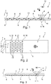
Fig. 1 : an example of an ingenious optical device in a sectional view, -
Fig. 2 : the optical device ofFig. 1 in a plan view of the substrate, -
Fig. 3 is a variant of the optical device according toFigures 1 and 2 with an interlayer arranged between the substrate and the optical structure. -
Figure 1 shows a schematic representation of an ingenious optical device 1 that can be used in a household appliance not shown in more detail in the figures. The optical device 1 comprises asubstrate 2 made of a translucent glass, which is preferably flat and longitudinal in shape. It is advisable to use ceramic glass. An optical structure 3 is printed on alower side 5 ofsubstrate 2. The term "lower side" refers to a possible position of use of optical device 1 or to a possible installation state of optical device 1 in the household appliance. - The optical structure 3 comprises a plurality of lens-shaped
optical elements 4, whereby in the example ofFigure 1 only one suchoptical element 4 is shown for reasons of clarity. It can be seen that the optical structure 3 or the lenticularoptical elements 4 can be designed asprojections 15 with spherical segment geometry projecting from thelower side 5 ofsubstrate 2. - The optical structure 3 with the lens-shaped
optical elements 4 is applied tosubstrate 2 by means of a non-contact printing method. A hybrid polymer can be used as a material for theoptical elements 4, which is suitable for contactless printing. A compound, the 3-glycidyloxy-propyltrimethoxysilane (GLYMO), a photoacid and BYK-33 is particularly suitable. - To ensure that the non-contact printed
optical elements 4 have the required lens shape, it is necessary that the deposited drops have a spherical shape. Thus the drops are pretreated to achieve a superhydrophobic surface where the drops forming theoptical elements 4 will remain as spherical as possible. This pretreatment can consist of several steps. In a first step, the glass can be cleaned to ensure a proper surface. In a further step the surface of the substrate can be activated. This can be achieved by introducing the glass in an O3 chamber during some time, preferably more than 60 minutes. Alternatively, a Pyrosil flame can be used as well to deposit a silane layer that modifies the surface tension. In a next step, fluorosilanes (1H, 1H, 2H, 2H-perfluorooctyltrichlorosilanes, PFOTCISi) can be deposited on the surface by a CVD technique. Around 5 microlitres of the fluorosilane can be deposited in a glass surface inside the chamber where the glass to be coated is also introduced. Vacuum is created in the chamber and during 30 minutes the fluorosilane evaporates and is deposited over the surface of the glass to be coated. In a last step of the pre-treatment, the substrate for at least 10 minutes at a temperature of about 110 °C. - Adjacent to a
lateral edge 6 of substrate 2 alight source 7 is provided, for example in the form of one or more LEDs emitting light 8 which is coupled into thetransparent substrate 2 so that it can propagate insubstrate 2. Thelight source 7 can be arranged laterally, i.e. in a lateral extension ofsubstrate 2 adjacent to it. The refractive index of the material ofsubstrate 2 is preferably selected such that thelight 8 cannot or only to a negligible extent reach theenvironment 9 of thesubstrate 2 fromsubstrate 2, but is totally reflected at theboundary surface 10 betweensubstrate 2 and theair 11 present in theenvironment 9.Substrate 2 thus follows the operating principle of a light waveguide. - As
Figure 1 shows, thelight 8 coupled intosubstrate 2 strikes theoptical element 4 after multiple reflections at theinterface 10. part of thelight 8 hitting theoptical element 4 is reflected at theinterface 11 betweensubstrate 2 and theoptical element 4, so that after reflection it strikes theinterface 11 betweensubstrate 10 and air 12, passes through theinterface 11 and then exits into theouter environment 9, where it can be perceived by anobserver 14. -
Figure 2 shows that on thelower side 6 of the transparent substrate 2 a plurality ofoptical elements 4 can be arranged at a distance from each other. Theoptical elements 4 have a round geometry in the plan view ofsubstrate 2 along the viewing direction B. In the example ofFigure 2 ,optical elements 4 with circular geometry are shown as an example. An elliptical geometry is also conceivable (not shown). In the example ofFigure 2 , theoptical elements 4 are arranged in the form of a grid withseveral grid lines 13, whereby 2adjacent grid lines 13 can be arranged offset from one another along the direction of propagation oflight 8 in thesubstrate 2. This ensures that thegrid lines 13 facing away from thelight source 7 can also hitsufficient light 8. -
Figure 3 shows a further development of the example ofFigure 1 . In the optical device 1 ofFigure 3 , a light-conductingintermediate layer 16 is arranged between the optical structure with theoptical element 4 and thesubstrate 2. This means that the light emitted by thelight source 7 of the optical device 1 is coupled into theintermediate layer 16 according toFigure 3 and spreads there to theoptical element 4 with multiple total reflection. - For example, the compound already described above as a suitable material for optical structure 3, supplemented by a refractive index-increasing component such as SU8 or diphenyl-dimethoxysilane, can be considered as material for
intermediate layer 16. This ensures that thelight 8 propagating in theintermediate layer 16 is reflected on its way to theoptical element 4 at the interfaces to thesubstrate 2 orouter environment 9 so that it cannot exit theintermediate layer 16 before it hits theoptical element 4. Like the optical structure 3, theintermediate layer 16 can also be applied tosubstrate 2 by contactless printing. -
- 1 optical device
- 2 substrate
- 3 optical structure
- 4 optical element
- 5 lower side
- 6 border
- 7 light source
- 8 light
- 9 environment
- 10 interface (substrate/environment)
- 11 Interface (substrate/optical element)
- 12 air
- 13 raster line
- 14 observer
- 15 projection
- 16 intermediate layer
- B direction of view
Claims (13)
- Method for manufacturing an optical device (1) for a household appliance, comprising the following steps: a) providing a substrate (2) of translucent glass; b) contactlessly printing the substrate (2) with an optical structure (3) comprising a plurality of lenticular optical elements (4).
- The method according to claim 1, characterized in that a light-conducting intermediate layer (16) is applied to the substrate (2) by non-contact printing before contactless printing of the optical structure (3) according to step b).
- The method according to claim 1 or 2, characterized in that in step b) optical elements (4) are applied having a round, preferably elliptical or circular, geometry in a plan view of the substrate (2).
- The method according to any of claims 1 to 3, characterized in that the optical elements (4) provided in step b) have a convex geometry, preferably the geometry of a spherical segment, in a cross-section perpendicular to the surface of the substrate (2).
- The method according to any of the preceding claims, characterized in that the optical elements (4) of the optical structure (3) are printed in the form of spherical segment projections (15).
- The method according to any of the preceding claims, characterized in that the surface of the substrate (2) provided in step a) is subjected to a surface treatment prior to application of the optical structure (3) according to step b), in which the surface is cleaned, activated and provided with a hydrophobic surface coating.
- Optical device (1) for a household appliance, in particular manufactured by the method according to any of the preceding claims, the device comprising: - a substrate (2) of translucent glass; - an optical structure (3), preferably printed on the substrate (2), comprising a plurality of lenticular optical elements (4).
- Optical device according to claim 7, characterized in that the optical device (1) further comprises a light source (7) arranged laterally on the substrate (2) so that the light emitted by the light source (7) can be coupled into the substrate (2).
- Optical device according to claim 7 or 8, characterized in that a light-conducting interlayer (16) is arranged between the optical structure (3) and the substrate (2).
- Optical device according to any of claims 7 to 9, characterized in that the optical elements (4) of the optical structure (3) have a round, preferably elliptical or circular geometry, in a plan view of the substrate (2).
- Optical device according to any of claims 7 to 10, characterized in that the optical elements (4) of the optical structure (3) are each arranged at a distance from one another.
- Optical device according to any of claims 7 to 11, characterized in that the optical elements (4) of the optical structure (3) are formed as spherical segment projections (15).
- Optical device according to any of claims 7 to 11, characterized in that the optical elements (4) of the optical structure (3) each have a convex geometry, preferably the geometry of a spherical segment, in a cross-section perpendicular to the surface of the substrate (2).
Priority Applications (1)
| Application Number | Priority Date | Filing Date | Title |
|---|---|---|---|
| EP18382690.8A EP3628918B1 (en) | 2018-09-27 | 2018-09-27 | Method for manufacturing an optical device for a household appliance and optical device |
Applications Claiming Priority (1)
| Application Number | Priority Date | Filing Date | Title |
|---|---|---|---|
| EP18382690.8A EP3628918B1 (en) | 2018-09-27 | 2018-09-27 | Method for manufacturing an optical device for a household appliance and optical device |
Publications (2)
| Publication Number | Publication Date |
|---|---|
| EP3628918A1 true EP3628918A1 (en) | 2020-04-01 |
| EP3628918B1 EP3628918B1 (en) | 2025-01-22 |
Family
ID=63722329
Family Applications (1)
| Application Number | Title | Priority Date | Filing Date |
|---|---|---|---|
| EP18382690.8A Active EP3628918B1 (en) | 2018-09-27 | 2018-09-27 | Method for manufacturing an optical device for a household appliance and optical device |
Country Status (1)
| Country | Link |
|---|---|
| EP (1) | EP3628918B1 (en) |
Citations (4)
| Publication number | Priority date | Publication date | Assignee | Title |
|---|---|---|---|---|
| US6833960B1 (en) * | 2001-03-05 | 2004-12-21 | Serigraph Inc. | Lenticular imaging system |
| EP1505414A1 (en) * | 2003-08-08 | 2005-02-09 | Schott AG | Method for producing scattering structures on planar lightguides |
| US20110116152A1 (en) * | 2008-05-13 | 2011-05-19 | Franck Guigan | Printed Optical Members |
| EP2631686A1 (en) * | 2009-02-14 | 2013-08-28 | LUXeXcel Holding BV. | Device for directing light beams, illustration device, method for producing a device and an illustration device |
Family Cites Families (3)
| Publication number | Priority date | Publication date | Assignee | Title |
|---|---|---|---|---|
| GB9800668D0 (en) * | 1998-01-13 | 1998-03-11 | Nashua Corp | Enhanced microlens screens |
| FR2940966B1 (en) * | 2009-01-09 | 2011-03-04 | Saint Gobain | HYDROPHOBIC SUBSTRATE COMPRISING A PLASMA ACTIVATED SILICON OXYCARBIDE PREMIUM |
| CN110050087A (en) * | 2016-12-12 | 2019-07-23 | Bsh家用电器有限公司 | Method for coating base elements for household appliance components and household appliance components |
-
2018
- 2018-09-27 EP EP18382690.8A patent/EP3628918B1/en active Active
Patent Citations (4)
| Publication number | Priority date | Publication date | Assignee | Title |
|---|---|---|---|---|
| US6833960B1 (en) * | 2001-03-05 | 2004-12-21 | Serigraph Inc. | Lenticular imaging system |
| EP1505414A1 (en) * | 2003-08-08 | 2005-02-09 | Schott AG | Method for producing scattering structures on planar lightguides |
| US20110116152A1 (en) * | 2008-05-13 | 2011-05-19 | Franck Guigan | Printed Optical Members |
| EP2631686A1 (en) * | 2009-02-14 | 2013-08-28 | LUXeXcel Holding BV. | Device for directing light beams, illustration device, method for producing a device and an illustration device |
Also Published As
| Publication number | Publication date |
|---|---|
| EP3628918B1 (en) | 2025-01-22 |
Similar Documents
| Publication | Publication Date | Title |
|---|---|---|
| KR101923236B1 (en) | Illuminated glass-ceramic item | |
| US20140268875A1 (en) | Shaped Optical Waveguide Bodies | |
| CN102906608A (en) | Light guide device | |
| JP5152928B2 (en) | Partition plate device | |
| JP2008508556A (en) | Flat fiber optic emitter | |
| EP2472309A3 (en) | Display apparatus having a backlight unit with uniform brightness | |
| US10690830B2 (en) | Light guide, display device, and game machine | |
| CN110463345B (en) | Optical system and induction cooker comprising same | |
| JP2012243753A (en) | Light guide plate structure | |
| US10249223B2 (en) | Light flux controlling member, light emitting device and illumination apparatus | |
| EP3628918B1 (en) | Method for manufacturing an optical device for a household appliance and optical device | |
| US20150138654A1 (en) | Fresnel lens with light-scattering preventive feature | |
| JP2017126586A (en) | Lighting device | |
| JP6138644B2 (en) | Lighting device | |
| JP6274974B2 (en) | Luminous flux control member, light emitting device, and illumination device | |
| JP6808031B2 (en) | Light guide plate, backlight module and display device | |
| US20060158746A1 (en) | System and method for extending viewing angle of light emitted from light pipe | |
| JP2009032474A (en) | Luminescent panel device | |
| CN107644601A (en) | Display device and the refrigerator for possessing the display device | |
| JP2015065062A (en) | Lighting device | |
| KR20100010629A (en) | Light guide plate for external ornament | |
| TW202238189A (en) | Optical fiber fabric device | |
| TW201317643A (en) | Light guide plate and light emitting device having same | |
| CN107110471B (en) | Optical element and light-emitting device having the same | |
| CN204285326U (en) | light guide |
Legal Events
| Date | Code | Title | Description |
|---|---|---|---|
| PUAI | Public reference made under article 153(3) epc to a published international application that has entered the european phase |
Free format text: ORIGINAL CODE: 0009012 |
|
| STAA | Information on the status of an ep patent application or granted ep patent |
Free format text: STATUS: THE APPLICATION HAS BEEN PUBLISHED |
|
| AK | Designated contracting states |
Kind code of ref document: A1 Designated state(s): AL AT BE BG CH CY CZ DE DK EE ES FI FR GB GR HR HU IE IS IT LI LT LU LV MC MK MT NL NO PL PT RO RS SE SI SK SM TR |
|
| AX | Request for extension of the european patent |
Extension state: BA ME |
|
| STAA | Information on the status of an ep patent application or granted ep patent |
Free format text: STATUS: REQUEST FOR EXAMINATION WAS MADE |
|
| 17P | Request for examination filed |
Effective date: 20201001 |
|
| RBV | Designated contracting states (corrected) |
Designated state(s): AL AT BE BG CH CY CZ DE DK EE ES FI FR GB GR HR HU IE IS IT LI LT LU LV MC MK MT NL NO PL PT RO RS SE SI SK SM TR |
|
| RAP1 | Party data changed (applicant data changed or rights of an application transferred) |
Owner name: BSH HAUSGERAETE GMBH |
|
| STAA | Information on the status of an ep patent application or granted ep patent |
Free format text: STATUS: EXAMINATION IS IN PROGRESS |
|
| 17Q | First examination report despatched |
Effective date: 20211210 |
|
| GRAP | Despatch of communication of intention to grant a patent |
Free format text: ORIGINAL CODE: EPIDOSNIGR1 |
|
| STAA | Information on the status of an ep patent application or granted ep patent |
Free format text: STATUS: GRANT OF PATENT IS INTENDED |
|
| INTG | Intention to grant announced |
Effective date: 20240926 |
|
| GRAS | Grant fee paid |
Free format text: ORIGINAL CODE: EPIDOSNIGR3 |
|
| GRAA | (expected) grant |
Free format text: ORIGINAL CODE: 0009210 |
|
| STAA | Information on the status of an ep patent application or granted ep patent |
Free format text: STATUS: THE PATENT HAS BEEN GRANTED |
|
| AK | Designated contracting states |
Kind code of ref document: B1 Designated state(s): AL AT BE BG CH CY CZ DE DK EE ES FI FR GB GR HR HU IE IS IT LI LT LU LV MC MK MT NL NO PL PT RO RS SE SI SK SM TR |
|
| REG | Reference to a national code |
Ref country code: GB Ref legal event code: FG4D |
|
| REG | Reference to a national code |
Ref country code: CH Ref legal event code: EP |
|
| REG | Reference to a national code |
Ref country code: IE Ref legal event code: FG4D |
|
| REG | Reference to a national code |
Ref country code: DE Ref legal event code: R096 Ref document number: 602018078643 Country of ref document: DE |
|
| REG | Reference to a national code |
Ref country code: NL Ref legal event code: MP Effective date: 20250122 |
|
| PG25 | Lapsed in a contracting state [announced via postgrant information from national office to epo] |
Ref country code: NL Free format text: LAPSE BECAUSE OF FAILURE TO SUBMIT A TRANSLATION OF THE DESCRIPTION OR TO PAY THE FEE WITHIN THE PRESCRIBED TIME-LIMIT Effective date: 20250122 |
|
| PG25 | Lapsed in a contracting state [announced via postgrant information from national office to epo] |
Ref country code: RS Free format text: LAPSE BECAUSE OF FAILURE TO SUBMIT A TRANSLATION OF THE DESCRIPTION OR TO PAY THE FEE WITHIN THE PRESCRIBED TIME-LIMIT Effective date: 20250422 |
|
| PG25 | Lapsed in a contracting state [announced via postgrant information from national office to epo] |
Ref country code: FI Free format text: LAPSE BECAUSE OF FAILURE TO SUBMIT A TRANSLATION OF THE DESCRIPTION OR TO PAY THE FEE WITHIN THE PRESCRIBED TIME-LIMIT Effective date: 20250122 |
|
| PG25 | Lapsed in a contracting state [announced via postgrant information from national office to epo] |
Ref country code: PL Free format text: LAPSE BECAUSE OF FAILURE TO SUBMIT A TRANSLATION OF THE DESCRIPTION OR TO PAY THE FEE WITHIN THE PRESCRIBED TIME-LIMIT Effective date: 20250122 |
|
| PG25 | Lapsed in a contracting state [announced via postgrant information from national office to epo] |
Ref country code: ES Free format text: LAPSE BECAUSE OF FAILURE TO SUBMIT A TRANSLATION OF THE DESCRIPTION OR TO PAY THE FEE WITHIN THE PRESCRIBED TIME-LIMIT Effective date: 20250122 |
|
| REG | Reference to a national code |
Ref country code: LT Ref legal event code: MG9D |
|
| PG25 | Lapsed in a contracting state [announced via postgrant information from national office to epo] |
Ref country code: IS Free format text: LAPSE BECAUSE OF FAILURE TO SUBMIT A TRANSLATION OF THE DESCRIPTION OR TO PAY THE FEE WITHIN THE PRESCRIBED TIME-LIMIT Effective date: 20250522 Ref country code: NO Free format text: LAPSE BECAUSE OF FAILURE TO SUBMIT A TRANSLATION OF THE DESCRIPTION OR TO PAY THE FEE WITHIN THE PRESCRIBED TIME-LIMIT Effective date: 20250422 |
|
| REG | Reference to a national code |
Ref country code: AT Ref legal event code: MK05 Ref document number: 1761713 Country of ref document: AT Kind code of ref document: T Effective date: 20250122 |
|
| PG25 | Lapsed in a contracting state [announced via postgrant information from national office to epo] |
Ref country code: HR Free format text: LAPSE BECAUSE OF FAILURE TO SUBMIT A TRANSLATION OF THE DESCRIPTION OR TO PAY THE FEE WITHIN THE PRESCRIBED TIME-LIMIT Effective date: 20250122 |
|
| PG25 | Lapsed in a contracting state [announced via postgrant information from national office to epo] |
Ref country code: LV Free format text: LAPSE BECAUSE OF FAILURE TO SUBMIT A TRANSLATION OF THE DESCRIPTION OR TO PAY THE FEE WITHIN THE PRESCRIBED TIME-LIMIT Effective date: 20250122 Ref country code: PT Free format text: LAPSE BECAUSE OF FAILURE TO SUBMIT A TRANSLATION OF THE DESCRIPTION OR TO PAY THE FEE WITHIN THE PRESCRIBED TIME-LIMIT Effective date: 20250522 |
|
| PG25 | Lapsed in a contracting state [announced via postgrant information from national office to epo] |
Ref country code: BG Free format text: LAPSE BECAUSE OF FAILURE TO SUBMIT A TRANSLATION OF THE DESCRIPTION OR TO PAY THE FEE WITHIN THE PRESCRIBED TIME-LIMIT Effective date: 20250122 Ref country code: GR Free format text: LAPSE BECAUSE OF FAILURE TO SUBMIT A TRANSLATION OF THE DESCRIPTION OR TO PAY THE FEE WITHIN THE PRESCRIBED TIME-LIMIT Effective date: 20250423 |
|
| PG25 | Lapsed in a contracting state [announced via postgrant information from national office to epo] |
Ref country code: AT Free format text: LAPSE BECAUSE OF FAILURE TO SUBMIT A TRANSLATION OF THE DESCRIPTION OR TO PAY THE FEE WITHIN THE PRESCRIBED TIME-LIMIT Effective date: 20250122 |
|
| PG25 | Lapsed in a contracting state [announced via postgrant information from national office to epo] |
Ref country code: SE Free format text: LAPSE BECAUSE OF FAILURE TO SUBMIT A TRANSLATION OF THE DESCRIPTION OR TO PAY THE FEE WITHIN THE PRESCRIBED TIME-LIMIT Effective date: 20250122 |
|
| PG25 | Lapsed in a contracting state [announced via postgrant information from national office to epo] |
Ref country code: SM Free format text: LAPSE BECAUSE OF FAILURE TO SUBMIT A TRANSLATION OF THE DESCRIPTION OR TO PAY THE FEE WITHIN THE PRESCRIBED TIME-LIMIT Effective date: 20250122 |
|
| PG25 | Lapsed in a contracting state [announced via postgrant information from national office to epo] |
Ref country code: DK Free format text: LAPSE BECAUSE OF FAILURE TO SUBMIT A TRANSLATION OF THE DESCRIPTION OR TO PAY THE FEE WITHIN THE PRESCRIBED TIME-LIMIT Effective date: 20250122 |
|
| PGFP | Annual fee paid to national office [announced via postgrant information from national office to epo] |
Ref country code: DE Payment date: 20250930 Year of fee payment: 8 |
|
| PG25 | Lapsed in a contracting state [announced via postgrant information from national office to epo] |
Ref country code: IT Free format text: LAPSE BECAUSE OF FAILURE TO SUBMIT A TRANSLATION OF THE DESCRIPTION OR TO PAY THE FEE WITHIN THE PRESCRIBED TIME-LIMIT Effective date: 20250122 |
|
| PGFP | Annual fee paid to national office [announced via postgrant information from national office to epo] |
Ref country code: GB Payment date: 20250923 Year of fee payment: 8 |
|
| PGFP | Annual fee paid to national office [announced via postgrant information from national office to epo] |
Ref country code: FR Payment date: 20250926 Year of fee payment: 8 |
|
| PG25 | Lapsed in a contracting state [announced via postgrant information from national office to epo] |
Ref country code: EE Free format text: LAPSE BECAUSE OF FAILURE TO SUBMIT A TRANSLATION OF THE DESCRIPTION OR TO PAY THE FEE WITHIN THE PRESCRIBED TIME-LIMIT Effective date: 20250122 Ref country code: CZ Free format text: LAPSE BECAUSE OF FAILURE TO SUBMIT A TRANSLATION OF THE DESCRIPTION OR TO PAY THE FEE WITHIN THE PRESCRIBED TIME-LIMIT Effective date: 20250122 |
|
| REG | Reference to a national code |
Ref country code: DE Ref legal event code: R097 Ref document number: 602018078643 Country of ref document: DE |
|
| PG25 | Lapsed in a contracting state [announced via postgrant information from national office to epo] |
Ref country code: RO Free format text: LAPSE BECAUSE OF FAILURE TO SUBMIT A TRANSLATION OF THE DESCRIPTION OR TO PAY THE FEE WITHIN THE PRESCRIBED TIME-LIMIT Effective date: 20250122 |
|
| PG25 | Lapsed in a contracting state [announced via postgrant information from national office to epo] |
Ref country code: SK Free format text: LAPSE BECAUSE OF FAILURE TO SUBMIT A TRANSLATION OF THE DESCRIPTION OR TO PAY THE FEE WITHIN THE PRESCRIBED TIME-LIMIT Effective date: 20250122 |
|
| PLBE | No opposition filed within time limit |
Free format text: ORIGINAL CODE: 0009261 |
|
| STAA | Information on the status of an ep patent application or granted ep patent |
Free format text: STATUS: NO OPPOSITION FILED WITHIN TIME LIMIT |
|
| REG | Reference to a national code |
Ref country code: CH Ref legal event code: L10 Free format text: ST27 STATUS EVENT CODE: U-0-0-L10-L00 (AS PROVIDED BY THE NATIONAL OFFICE) Effective date: 20251203 |
|
| 26N | No opposition filed |
Effective date: 20251023 |
|
| REG | Reference to a national code |
Ref country code: CH Ref legal event code: H13 Free format text: ST27 STATUS EVENT CODE: U-0-0-H10-H13 (AS PROVIDED BY THE NATIONAL OFFICE) Effective date: 20260504 |