EP3627696A2 - Frequency comb generating device and method for generating a frequency comb - Google Patents
Frequency comb generating device and method for generating a frequency comb Download PDFInfo
- Publication number
- EP3627696A2 EP3627696A2 EP19180332.9A EP19180332A EP3627696A2 EP 3627696 A2 EP3627696 A2 EP 3627696A2 EP 19180332 A EP19180332 A EP 19180332A EP 3627696 A2 EP3627696 A2 EP 3627696A2
- Authority
- EP
- European Patent Office
- Prior art keywords
- electromagnetic wave
- optical
- frequency comb
- switching unit
- light receiving
- Prior art date
- Legal status (The legal status is an assumption and is not a legal conclusion. Google has not performed a legal analysis and makes no representation as to the accuracy of the status listed.)
- Granted
Links
Images


Classifications
-
- H—ELECTRICITY
- H01—ELECTRIC ELEMENTS
- H01S—DEVICES USING THE PROCESS OF LIGHT AMPLIFICATION BY STIMULATED EMISSION OF RADIATION [LASER] TO AMPLIFY OR GENERATE LIGHT; DEVICES USING STIMULATED EMISSION OF ELECTROMAGNETIC RADIATION IN WAVE RANGES OTHER THAN OPTICAL
- H01S3/00—Lasers, i.e. devices using stimulated emission of electromagnetic radiation in the infrared, visible or ultraviolet wave range
- H01S3/005—Optical devices external to the laser cavity, specially adapted for lasers, e.g. for homogenisation of the beam or for manipulating laser pulses, e.g. pulse shaping
- H01S3/0085—Modulating the output, i.e. the laser beam is modulated outside the laser cavity
-
- G—PHYSICS
- G02—OPTICS
- G02F—OPTICAL DEVICES OR ARRANGEMENTS FOR THE CONTROL OF LIGHT BY MODIFICATION OF THE OPTICAL PROPERTIES OF THE MEDIA OF THE ELEMENTS INVOLVED THEREIN; NON-LINEAR OPTICS; FREQUENCY-CHANGING OF LIGHT; OPTICAL LOGIC ELEMENTS; OPTICAL ANALOGUE/DIGITAL CONVERTERS
- G02F1/00—Devices or arrangements for the control of the intensity, colour, phase, polarisation or direction of light arriving from an independent light source, e.g. switching, gating or modulating; Non-linear optics
- G02F1/35—Non-linear optics
- G02F1/353—Frequency conversion, i.e. wherein a light beam is generated with frequency components different from those of the incident light beams
-
- H—ELECTRICITY
- H01—ELECTRIC ELEMENTS
- H01S—DEVICES USING THE PROCESS OF LIGHT AMPLIFICATION BY STIMULATED EMISSION OF RADIATION [LASER] TO AMPLIFY OR GENERATE LIGHT; DEVICES USING STIMULATED EMISSION OF ELECTROMAGNETIC RADIATION IN WAVE RANGES OTHER THAN OPTICAL
- H01S3/00—Lasers, i.e. devices using stimulated emission of electromagnetic radiation in the infrared, visible or ultraviolet wave range
- H01S3/09—Processes or apparatus for excitation, e.g. pumping
- H01S3/091—Processes or apparatus for excitation, e.g. pumping using optical pumping
- H01S3/094—Processes or apparatus for excitation, e.g. pumping using optical pumping by coherent light
- H01S3/094076—Pulsed or modulated pumping
-
- H—ELECTRICITY
- H01—ELECTRIC ELEMENTS
- H01S—DEVICES USING THE PROCESS OF LIGHT AMPLIFICATION BY STIMULATED EMISSION OF RADIATION [LASER] TO AMPLIFY OR GENERATE LIGHT; DEVICES USING STIMULATED EMISSION OF ELECTROMAGNETIC RADIATION IN WAVE RANGES OTHER THAN OPTICAL
- H01S3/00—Lasers, i.e. devices using stimulated emission of electromagnetic radiation in the infrared, visible or ultraviolet wave range
- H01S3/10—Controlling the intensity, frequency, phase, polarisation or direction of the emitted radiation, e.g. switching, gating, modulating or demodulating
- H01S3/11—Mode locking; Q-switching; Other giant-pulse techniques, e.g. cavity dumping
-
- H—ELECTRICITY
- H03—ELECTRONIC CIRCUITRY
- H03B—GENERATION OF OSCILLATIONS, DIRECTLY OR BY FREQUENCY-CHANGING, BY CIRCUITS EMPLOYING ACTIVE ELEMENTS WHICH OPERATE IN A NON-SWITCHING MANNER; GENERATION OF NOISE BY SUCH CIRCUITS
- H03B17/00—Generation of oscillations using radiation source and detector, e.g. with interposed variable obturator
-
- H—ELECTRICITY
- H04—ELECTRIC COMMUNICATION TECHNIQUE
- H04B—TRANSMISSION
- H04B10/00—Transmission systems employing electromagnetic waves other than radio-waves, e.g. infrared, visible or ultraviolet light, or employing corpuscular radiation, e.g. quantum communication
- H04B10/50—Transmitters
- H04B10/501—Structural aspects
- H04B10/506—Multiwavelength transmitters
-
- H—ELECTRICITY
- H04—ELECTRIC COMMUNICATION TECHNIQUE
- H04B—TRANSMISSION
- H04B10/00—Transmission systems employing electromagnetic waves other than radio-waves, e.g. infrared, visible or ultraviolet light, or employing corpuscular radiation, e.g. quantum communication
- H04B10/50—Transmitters
- H04B10/508—Pulse generation, e.g. generation of solitons
-
- G—PHYSICS
- G02—OPTICS
- G02F—OPTICAL DEVICES OR ARRANGEMENTS FOR THE CONTROL OF LIGHT BY MODIFICATION OF THE OPTICAL PROPERTIES OF THE MEDIA OF THE ELEMENTS INVOLVED THEREIN; NON-LINEAR OPTICS; FREQUENCY-CHANGING OF LIGHT; OPTICAL LOGIC ELEMENTS; OPTICAL ANALOGUE/DIGITAL CONVERTERS
- G02F2203/00—Function characteristic
- G02F2203/25—Frequency chirping of an optical modulator; Arrangements or methods for the pre-set or tuning thereof
-
- G—PHYSICS
- G02—OPTICS
- G02F—OPTICAL DEVICES OR ARRANGEMENTS FOR THE CONTROL OF LIGHT BY MODIFICATION OF THE OPTICAL PROPERTIES OF THE MEDIA OF THE ELEMENTS INVOLVED THEREIN; NON-LINEAR OPTICS; FREQUENCY-CHANGING OF LIGHT; OPTICAL LOGIC ELEMENTS; OPTICAL ANALOGUE/DIGITAL CONVERTERS
- G02F2203/00—Function characteristic
- G02F2203/56—Frequency comb synthesizer
Definitions
- Embodiments of the present disclosure relate generally to a frequency comb generating device, a method for generating an optical frequency comb as well as to a method for generating an electrical frequency comb.
- Optical or electrical frequency combs consist of a series of essentially equidistant electrical pulses which are approximately shaped as Dirac delta functions. These electrical frequency combs are often used for phase and amplitude calibration of spectrum analyzers or oscilloscopes, wherein the electrical combs serve as a known reference for the calibration process.
- the reference frequency comb For the generation of the reference frequency comb, there are two seemingly contradictory requirements. On one hand, a certain minimum signal-to-noise ratio is required which is linked to a minimum power level of the electrical frequency comb.
- the power level of the electrical frequency comb in turn is determined by the number of pulses per time interval, i.e. the pulse frequency in time domain. A high power level therefore demands for a high pulse frequency in time domain.
- a very fine frequency comb is desired, i.e. the frequency interval between peaks in the frequency domain should be very small. This, however, corresponds to a large time interval between peaks in time domain as the intervals in time and frequency domain are inversely proportional to each other. Thus, a fine frequency comb in frequency domain requires a low pulse frequency in time domain.
- Embodiments of the present disclosure provide a frequency comb generating device.
- the frequency comb generating device comprises a pulsed optical light source, a sequence generator, a light receiving unit and a switching unit.
- the sequence generator is configured to generate a repeating sequence signal and to forward the repeating sequence signal at least to the switching unit.
- the pulsed optical light source is configured to generate electromagnetic wave packets.
- the pulsed optical light source is synchronized with the sequence generator.
- the light receiving unit is configured to receive the electromagnetic wave packets and to convert the electromagnetic wave packets into an electrical signal.
- the switching unit is configured to at least one of control the pulsed optical light source, control the light receiving unit, attenuate the electromagnetic wave packets, phase shift the electromagnetic wave packets, attenuate the electrical signal, and phase shift the electrical signal based on the repeating sequence signal.
- the switching unit alters the properties of an electrical frequency comb generated by the frequency comb generating device, in particular the pulsed optical light source, to the effect that the intervals between the individual Dirac functions in frequency domain are reduced, while still maintaining a high signal-to-noise ratio. Thereby, a fine electrical frequency comb with high signal-to-noise ratio is achieved.
- the electromagnetic wave packets received by the light receiving unit correspond to optical radiation or rather electromagnetic waves in the optical wavelength range, for instance between 100 nm and 1 mm.
- the term "light” is to be understood to be not restricted to the visible light range, but rather to also include the infrared and ultraviolet frequency ranges.
- the term "synchronized" means that the frequency at which the pulsed optical light sources generates the electromagnetic wave packets (i.e. the number of wave packets per time interval, not the frequency of the light itself) and the number of pieces of information (contained in the repeating sequence signal) generated per time interval have a predetermined ratio, for example one. Alternatively or additionally, there is a predetermined phase relation between the generation of a wave packet and the generation of a piece of information.
- phase shift of the electromagnetic wave packets and/or the phase shift of the electrical signal corresponds to delaying at least a certain signal portion in time. This becomes obvious since the pulsed optical light source may generate electromagnetic pulses wherein pulses can only be controlled with regard to amplitude and delay (phase).
- the switching unit may be assigned to different components of the frequency comb generating device so that the switching unit is enabled to interact with the optical light source directly.
- the switching unit is connected to the light receiving unit so as to control the light receiving unit.
- the switching unit is assigned to the optical part of the frequency comb generating device as the switching unit attenuates the electromagnetic wave packets and/or phase shifts the electromagnetic wave packets.
- the switching unit is assigned to the electrical part of the frequency comb generating device as the switching unit attenuates the electrical signal and/or phase shifts the electrical signal.
- the switching unit interacts with the respective component based on the repeating sequence signal generated by the sequence generator.
- the switching unit is configured to control the pulsed optical light source, to control the light receiving unit, to attenuate the electromagnetic wave packets, to phase shift the electromagnetic wave packets, to attenuate the electrical signal, and/or to phase shift the electrical signal.
- the switching unit is connected with the pulsed optical light source, the light receiving unit, the optical part of the frequency comb generating device and/or the electrical part of the frequency comb generating device.
- the sequence generator is configured to generate a pseudorandom binary sequence.
- the binary sequence may correspond to a digital signal.
- the individual pieces of information contained within the repeating sequence signal are "0" and "1", or at least can be mapped onto these two values, wherein the order of the individual pieces of information is pseudorandomly generated. After a predefined time interval, the same order may be repeated.
- the light receiving unit may be a photo diode.
- the electromagnetic wave packets are converted to at least one electrical signal in a particular energy efficient manner and in real time.
- the pulsed optical light source is an optical pulsed laser.
- Optical pulsed lasers are capable of generating high intensity electromagnetic wave packets of particularly short duration, thereby optimally approximating a Dirac comb.
- sequence generator the light receiving unit and the switching unit are placed on a same chip or die.
- a compact frequency comb generating device is provided, as the respective components, namely the sequence generator, the light receiving unit and the switching unit, are located on a common chip or rather a common die.
- An optional control unit may also be located on the common chip or rather the common die
- the pulsed optical light source and the light receiving unit are optically connected with each other via an optical fibre. Due to the optical fibre, the pulsed optical light source and the light receiving unit do not need to be perfectly aligned. Thus, intensity losses due to misalignment and/or other perturbations is reduced or even eliminated which in turn simplifies the manufacturing of the frequency comb generating device.
- the switching unit is configured to control the pulsed optical light source to generate an electromagnetic wave packet for at least one certain current value of the repeating sequence signal and to not generate an electromagnetic wave packet for at least one other certain current value of the repeating sequence signal.
- the current value corresponds to the respective actual value of the repeating sequence signal.
- the resulting optical frequency comb in time domain is missing some of its teeth compared to a full optical frequency comb, which translates to a shorter distance between the individual Dirac functions in frequency domain.
- a fine optical frequency comb is achieved, which is then converted to a fine electrical frequency comb by the light receiving unit.
- the switching unit may be configured to control the pulsed optical light source to generate an electromagnetic wave packet for each bit of the binary sequence having one value of the two possible values and to not generate an electromagnetic wave packet for each bit having the other value of the two possible values.
- the switching unit may control the pulsed optical light source to generate an optical pulse for every "1" and to not generate an optical pulse for every "0" in the binary sequence, or vice versa.
- the switching unit is an electrical switch connected to the light receiving unit, the switching unit being positioned downstream of the light receiving unit.
- the switching unit is assigned to the electrical part of the frequency comb generating device.
- the switching unit is configured to attenuate and/or phase shift the electrical signals generated by the light receiving unit based on the current value of the repeating sequence signal.
- the switching unit is configured to cancel out an electrical pulse for at least one value and to not alter the electrical pulse for the other values. By cancelling out some of the electrical pulses, a fine electrical frequency comb is generated, as explained above.
- the switching unit may be a high-bandwidth electrical switch.
- the switching unit is an optical switch connected to the light receiving unit, the switching unit being positioned upstream of the light receiving unit.
- the switching unit is assigned to the optical part of the frequency comb generating device.
- the switching unit is configured to attenuate and/or phase shift the electromagnetic wave packets generated by the pulsed optical light source based on the current value of the repeating sequence signal.
- the switching unit is configured to cancel out an electromagnetic wave packet for at least one value and to not alter the electromagnetic wave packet for the other values. By cancelling out some of the electromagnetic wave packets, a fine optical frequency comb is generated, as explained above.
- the switching unit may be a high-bandwidth optical switch.
- the switching unit is configured to control the light receiving unit to convert the received electromagnetic wave packets into an electrical signal with predefined properties, wherein the predefined properties depend on the current value of the repeating sequence signal.
- the resulting electrical frequency comb is altered such that the intervals between the individual Dirac functions in frequency domain are lowered while still maintaining a high signal-to-noise ratio.
- the repeating sequence signal may comprise a ternary sequence.
- the individual pieces of information are "-1", “0” and “1", or at least the actual value can be mapped onto these three values.
- the switching unit is configured to control the light receiving unit to generate a positive voltage pulse, a negative voltage pulse or no voltage pulse based on the current value of the ternary sequence.
- the light receiving unit may generate a positive voltage electrical pulse for every "1", a negative voltage electrical pulse for every "-1” and may not generate an electrical pulse for every "0" in the ternary sequence.
- any other mapping of current values of the repeating sequence signal onto the properties of the electrical pulses is also possible. Once again, this results in a fine electrical frequency comb with a high signal-to-noise ratio.
- the light receiving unit is a switchable photo diode comprising two conversion elements, wherein the switching unit is configured to selectively activate the conversion elements based on the current value of the ternary sequence.
- one conversion element is configured to generate negative voltage pulse while the other one is configured to generate positive voltage pulses.
- the light receiving unit is a switchable photo diode comprising two conversion elements and a control unit, wherein the switching unit is configured to forward the repeating sequence signal to the control unit, and wherein the control unit is configured to selectively activate the two conversion elements based on the repeating sequence signal.
- one conversion element is configured to generate negative voltage pulses while the other one is configured to generate positive voltage pulses.
- Embodiments of the present disclosure also provide a method for generating an optical frequency comb, comprising the steps of: generating a repeating sequence signal; and generating optical electromagnetic wave packets; wherein parts of the optical electromagnetic wave packets are filtered out based on the repeating sequence signal or the step of generating the electromagnetic wave packets is controlled based on the repeating sequence signal.
- the optical frequency comb is obtained either by controlling a light source, in particular an optical pulsed light source, to directly generate the optical frequency comb, or by generating a full optical frequency comb and cancelling out some of the Dirac functions in time domain, as explained above.
- the resulting optical frequency comb in time domain is missing some of its teeth compared to a full optical frequency comb, which translates to a shorter distance between the individual Dirac functions in frequency domain.
- the modified optical frequency comb may then be forwarded to further devices, e.g. for the purpose of calibrating said devices.
- the repeating sequence signal comprises a binary or a ternary sequence.
- Embodiments of the present disclosure also provide a method for generating an electrical frequency comb, comprising the steps of: generating a repeating sequence signal; generating optical electromagnetic wave packets; receiving the optical electromagnetic wave packets; and converting the optical electromagnetic wave packets into an electrical signal; wherein parts of the optical electromagnetic wave packets or parts of the electrical signal are filtered out based on the repeating sequence signal, or wherein the step of generating the electromagnetic wave packets is controlled based on the repeating sequence signal or the steps of receiving and converting the optical electromagnetic wave packets are controlled based on the repeating sequence signal.
- the method for generating an electrical frequency comb may comprise the method for generating an optical frequency comb at least in parts, as a repeating sequence signal and optical electromagnetic wave packets are generated. Further, parts of the optical electromagnetic wave packets are filtered out based on the repeating sequence signal or the step of generating the electromagnetic wave packets is controlled based on the repeating sequence signal.
- the method for generating an electrical frequency comb may be rewritten as performing the method for generating an optical frequency comb as defined above, wherein the optical electromagnetic wave packets are received and converted into an electrical signal.
- parts of the electrical signal are filtered out based on the repeating sequence signal or the step of generating the electromagnetic wave packets is controlled based on the repeating sequence signal or the steps of receiving and converting the optical electromagnetic wave packets are controlled based on the repeating sequence signal.
- the repeating sequence signal comprises a binary or a ternary sequence.
- the term "light” is to be understood to be not restricted to the visible light range, but rather to also include the infrared and ultraviolet frequency ranges.
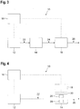
- FIGS 1 to 4 schematically show different variants of a frequency comb generating device 10.
- the frequency comb generating device 10 comprises a pulsed optical light source 12, a light receiving unit 14, a sequence generator 16, and a switching unit 18.
- dotted lines represent a connection that is signal transmitting in an arbitrary way. This may include wired or wireless communication between the individual device functional units, also called components. Dashed lines represent an optical connection, i.e. light may be transported between the different devices over air, through vacuum and/or via one or several optical fibres. Finally, solid lines represent an electrical wire-based connection. When an arrow is attached to a connecting line, it is to be understood that this arrow depicts the travel direction of a corresponding optical signal or electrical signal, respectively.
- the sequence generator 16 is configured to generate a repeating sequence signal and to forward the repeating sequence signal to the switching unit 18 to which the sequence generator 16 is connected in a signal transmitting manner.
- the repeating sequence may comprise a binary and/or a ternary sequence, which repeats after a predefined time interval, wherein the individual pieces of information are generated with a sequence frequency f S .
- the sequence generator 16 generates pieces of information with a frequency f S , wherein each piece of information may have one of two or one of three values, respectively.
- the repeating sequence may be a pseudorandom binary sequence (PRBS).
- PRBS pseudorandom binary sequence
- the pulsed optical light source 12 is configured to generate electromagnetic wave packets, which will be referred to as optical pulses in the following.
- the optical light source 12 is configured to generate short or ultrashort optical pulses, i.e. the width of the individual pulses is much smaller than the time between two pulses even for high frequencies f p .
- the optical light source 12 may be an optical pulsed laser.
- each optical pulse typically has the form of a sinusoid, wherein the maximum amplitude is confined by a Gaussian function.
- each optical pulse will be approximated to have the form of a Dirac function in the following.
- the ratio n is equal to 1, which means that the optical pulses and the individual pieces of information contained in the repeating sequence signal are generated with the same frequency.
- optical light source 12 and the sequence generator 16 may be synchronized with respect to phase, which means that there is a predetermined time delay interval between the generation of an optical pulse and a corresponding piece of information contained in the repeating sequence signal.
- the light receiving unit 14 is configured to receive the electromagnetic wave packets, i.e. the optical pulses, and to convert the optical pulses into a corresponding electrical signal.
- the light receiving unit 14 is a photo diode.
- the functionality of the switching unit 18 at least partly depends on the embodiment, and will be described in more detail in the following for each embodiment of the frequency comb generating device 10 with respect to Figures 1 to 4 .
- the switching unit 18 is configured to control the pulsed optical light source 12 based on the repeating sequence signal generated by the sequence generator 16, more specifically based on the current value of the repeating sequence signal.
- the switching unit 18 may be separate from the sequence generator 16 and the pulsed optical light source 12. Alternatively, the switching unit 18 may be integrated into the sequence generator 16 or into the pulsed optical light source 12.
- the pulsed optical light source 12, the sequence generator 16 and/or the switching unit 18 may be formed integrally with each other so that the respective components are housed in a common housing.
- an electrical frequency comb 20 with known characteristics is generated as explained in the following with reference to Figures 1 and 5 .
- the repeating sequence signal is generated via the sequence generator as described above (step S1 a ).
- the switching unit 18 controls the pulsed optical light source 12 to generate an optical pulse every time the current piece of information contained in the repeating sequence signal is equal to at least one of the possible values and to not generate an optical pulse when the current piece of information contained in the repeating sequence signal is equal to one of the other possible values (step S2 a ).
- the switching unit 18 may control the pulsed optical light source 12 to generate an optical pulse for every "1” and to not generate an optical pulse for every "0" in the binary sequence, or vice versa.
- the pulsed optical light source 12 would generate optical pulses at a frequency f p which would result in an optical frequency comb 22 with a spacing of f p of the individual Dirac functions in the frequency domain.
- step S2 a is a modified optical frequency comb 22' with a spacing between the individual Dirac functions that is much smaller than f p and that has a high signal-to-noise ratio.
- the modified optical frequency comb 22' is then received (step S3 a ) and converted to the electrical frequency comb 20 (step S4 a ) via the light receiving unit 14.
- step S4 a i.e. the electrical frequency comb 20
- the result of step S4 a is characterized by a small spacing between the individual Dirac functions in the frequency domain and by a high signal-to-noise ratio.
- the switching unit 18 is an optical switch that is connected to the pulsed optical light source 12 and to the light receiving unit 14.
- the switching unit 18 is positioned downstream of the pulsed optical light source 12 and upstream of the light receiving unit 14. Put it another way, the switching unit 18 is positioned between the pulsed optical light source 12 and the light receiving unit 14.
- the switching unit 18 is configured to attenuate and/or phase shift the optical pulses, also called electromagnetic wave packets, generated by the pulsed optical light source 12 based on the current value of the repeating sequence signal.
- an electrical frequency comb 20 with known characteristics is generated as explained in the following with reference to Figures 2 and 6 .
- the repeating sequence signal is generated via the sequence generator as described above (step S1 b ).
- optical pulses are generated via the optical light source 12 at a frequency f p (step S2 b ), which results in an optical frequency comb 22 with a spacing of f p of the individual Dirac functions in the frequency domain.
- the switching unit 18 filters the optical frequency comb 22 based on the current value of the repeating frequency signal (step S3 b ).
- the switching unit 18 attenuates and/or phase shifts an optical pulse passing the switching unit 18 every time the current piece of information contained in the repeating sequence signal is equal to at least one of the possible values and does not alter the optical pulse when the current piece of information contained in the repeating sequence signal is equal to one of the other possible values.
- the switching unit 18 may alter the optical pulse for every "1” and may not alter the optical pulse for every "0" in the binary sequence, or vice versa.
- the switching unit 18 completely filters out some of the optical pulses based on the respective value of the repeating sequence signal.
- step S3 b is a modified optical frequency comb 22' that is equivalent to the one described above in the context of the first possible embodiment.
- step S3 b receives the modified optical frequency comb 22' (step S3 b ) and converting it to the electrical frequency comb 20 (step S4) via the light receiving unit 14.
- the switching unit 18 is an electrical switch that is connected to the light receiving unit 14 wherein the switching unit 18 is located downstream of the light receiving unit 14. Therefore, electrical signals generated by the light receiving unit 14 are forwarded to the switching unit 18.
- the switching unit 18 is configured to attenuate and/or phase shift the electrical pulses generated by the light receiving unit 14 based on the current value of the repeating sequence signal.
- an electrical frequency comb 20 with known characteristics is generated as explained in the following with reference to Figures 3 and 7 .
- the repeating sequence signal is generated via the sequence generator as described above (step S1 c ).
- optical pulses are generated via the optical light source 12 at a frequency f p (step S2 c ), which results in an optical frequency comb 22 with a spacing of f p of the individual Dirac functions in the frequency domain.
- the optical frequency comb 22 is converted to a corresponding intermediate electrical frequency comb 24 by the light receiving unit 14 (step S3 c ).
- the switching unit 18 filters the intermediate electrical frequency comb 24 based on the current value of the repeating frequency signal (step S4 c ).
- the switching unit 18 attenuates and/or phase shifts an electrical pulse passing the switching unit 18 every time the current piece of information contained in the repeating sequence signal is equal to at least one of the possible values and does not alter the electrical pulse when the current piece of information contained in the repeating sequence signal is equal to one of the other possible values.
- the switching unit 18 may alter the electrical pulse for every "1” and may not alter the optical pulse for every "0" in the binary sequence, or vice versa.
- the switching unit 18 completely filters out some of the electrical pulses based on the respective value of the repeating sequence signal.
- step S4 c is the electrical frequency comb 20 that is equivalent to the one described in the context of the first embodiment.
- the switching unit 18 is configured to control the light receiving unit 14 based on the repeating sequence signal, more specifically based on the current value of the repeating sequence signal.
- the switching unit 18 may be separate from the sequence generator 16 and the light receiving unit 14. Alternatively, the switching unit 18 may be integrated into the sequence generator 16 or into the light receiving unit 14.
- the light receiving unit 14, the sequence generator 16 and the switching unit 18 may be placed on a same chip or a same die, also called common chip or rather common die. Hence, a compact frequency comb generating device 10 is obtained.
- an electrical frequency comb 20 with known characteristics is generated as explained in the following with reference to Figures 4 and 8 .
- the repeating sequence signal is generated via the sequence generator 16 as described above (step S1 d ).
- optical pulses are generated via the optical light source 12 at a frequency f p (step S2 d ), which results in an optical frequency comb 22 with a spacing of f p of the individual Dirac functions in the frequency domain.
- optical pulses are then received via the light receiving unit 14 (step S3 d ), wherein the light receiving unit 14 is controlled by the switching unit 18 to convert each of the received optical pulses into a corresponding electrical pulse with predefined properties (step S4 d ), thereby generating the electrical frequency comb 20.
- step S4 d the predefined properties of each electrical pulse depend on the current value of the repeating sequence signal.
- the light receiving unit 14 generates an electrical pulse every time the current piece of information contained in the repeating sequence signal is equal to at least one of the possible values and does not generate an electrical pulse when the current piece of information contained in the repeating sequence signal is equal to one of the other possible values.
- the repeating sequence is a binary sequence
- the possible individual pieces of information will be "0" and "1".
- the light receiving unit 14 may generate an electrical pulse for every "1” and may not generate an electrical pulse for every "0" in the binary sequence, or vice versa.
- the individual pieces of information will be "-1", "0" and "1", or at least the actual values can be mapped to these three values.
- the light receiving unit 14 may generate a positive voltage electrical pulse for every "1", a negative voltage electrical pulse for every "-1" and may not generate an electrical pulse for every "0" in the ternary sequence.
- any other mapping of current values of the repeating sequence signal onto the properties of the electrical pulses is also possible.
- the light receiving unit 14 may comprise a first conversion element 26 being configured to generate positive voltage electrical pulses and a second conversion element 28 being configured to generate negative voltage electrical pulses.
- the switching unit 18 may be configured to selectively activate one of the two conversion elements 26, 28 based on the current value of the ternary sequence.
- the light receiving unit 14 may comprise a control unit 30 being configured to selectively activate the conversion elements 26, 28 based on a corresponding control signal received from the switching unit 18.
- control unit 30 is part of the light receiving unit 14, the control unit 30 may also be located on the same chip or rather the same die.
- the switching unit 18 may be assigned to different components of the frequency comb generating device 10 that comprise an optical part and an electrical part which are separated by the light receiving unit 14.
- the variants shown in Figures 1 and 2 illustrate that the switching unit 18 is assigned to the optical part of the frequency comb generating device 10 whereas the switching unit 18 is assigned to the electrical part of the frequency comb generating device 10 in the variant shown in Figure 3 .
- the variant according to Figure 4 illustrates that the switching unit 18 is assigned to the light receiving unit 14 itself while controlling the light receiving unit 14.
- the converting properties may be controlled via the switching unit 18.
- Parts of the frequency comb generating device 10 as shown in Figures 1 and 2 in particular the pulsed optical light source 12, the sequence generator 16 and the switching unit 18, may also be used to only generate the modified optical frequency comb 22', i.e. conversion of the modified optical frequency comb 22' into the electrical frequency comb 20 may be omitted.
- the resulting modified optical frequency comb 22' in time domain is missing some of its teeth compared to a full optical frequency comb, which translates to a shorter distance between the individual Dirac functions in frequency domain.
- a fine modified optical frequency comb 22' is achieved.
- the modified optical frequency comb 22' may then be forwarded to further devices, e.g. for the purpose of calibrating said devices.
Landscapes
- Physics & Mathematics (AREA)
- Electromagnetism (AREA)
- Nonlinear Science (AREA)
- Engineering & Computer Science (AREA)
- Optics & Photonics (AREA)
- Computer Networks & Wireless Communication (AREA)
- Signal Processing (AREA)
- Plasma & Fusion (AREA)
- General Physics & Mathematics (AREA)
- Optical Communication System (AREA)
- Optical Modulation, Optical Deflection, Nonlinear Optics, Optical Demodulation, Optical Logic Elements (AREA)
Abstract
Description
- Embodiments of the present disclosure relate generally to a frequency comb generating device, a method for generating an optical frequency comb as well as to a method for generating an electrical frequency comb.
- Optical or electrical frequency combs consist of a series of essentially equidistant electrical pulses which are approximately shaped as Dirac delta functions. These electrical frequency combs are often used for phase and amplitude calibration of spectrum analyzers or oscilloscopes, wherein the electrical combs serve as a known reference for the calibration process.
- For the generation of the reference frequency comb, there are two seemingly contradictory requirements. On one hand, a certain minimum signal-to-noise ratio is required which is linked to a minimum power level of the electrical frequency comb. The power level of the electrical frequency comb in turn is determined by the number of pulses per time interval, i.e. the pulse frequency in time domain. A high power level therefore demands for a high pulse frequency in time domain.
- On the other hand, usually a very fine frequency comb is desired, i.e. the frequency interval between peaks in the frequency domain should be very small. This, however, corresponds to a large time interval between peaks in time domain as the intervals in time and frequency domain are inversely proportional to each other. Thus, a fine frequency comb in frequency domain requires a low pulse frequency in time domain.
- Therefore, there is a need for a frequency comb generating device as well as a method for generating an optical or an electrical frequency comb that are capable of generating fine frequency combs with a high signal-to-noise ratio.
- Embodiments of the present disclosure provide a frequency comb generating device. The frequency comb generating device comprises a pulsed optical light source, a sequence generator, a light receiving unit and a switching unit. The sequence generator is configured to generate a repeating sequence signal and to forward the repeating sequence signal at least to the switching unit. The pulsed optical light source is configured to generate electromagnetic wave packets. The pulsed optical light source is synchronized with the sequence generator. The light receiving unit is configured to receive the electromagnetic wave packets and to convert the electromagnetic wave packets into an electrical signal. The switching unit is configured to at least one of control the pulsed optical light source, control the light receiving unit, attenuate the electromagnetic wave packets, phase shift the electromagnetic wave packets, attenuate the electrical signal, and phase shift the electrical signal based on the repeating sequence signal.
- Through the combination of the pulsed optical light source with the light receiving unit, a high power level is achievable as the individual electromagnetic wave packets can be generated at a high frequency. The switching unit alters the properties of an electrical frequency comb generated by the frequency comb generating device, in particular the pulsed optical light source, to the effect that the intervals between the individual Dirac functions in frequency domain are reduced, while still maintaining a high signal-to-noise ratio. Thereby, a fine electrical frequency comb with high signal-to-noise ratio is achieved.
- In fact, the electromagnetic wave packets received by the light receiving unit correspond to optical radiation or rather electromagnetic waves in the optical wavelength range, for instance between 100 nm and 1 mm.
- Therein and in the following, the term "light" is to be understood to be not restricted to the visible light range, but rather to also include the infrared and ultraviolet frequency ranges.
- Moreover, the term "synchronized" means that the frequency at which the pulsed optical light sources generates the electromagnetic wave packets (i.e. the number of wave packets per time interval, not the frequency of the light itself) and the number of pieces of information (contained in the repeating sequence signal) generated per time interval have a predetermined ratio, for example one. Alternatively or additionally, there is a predetermined phase relation between the generation of a wave packet and the generation of a piece of information.
- The phase shift of the electromagnetic wave packets and/or the phase shift of the electrical signal corresponds to delaying at least a certain signal portion in time. This becomes obvious since the pulsed optical light source may generate electromagnetic pulses wherein pulses can only be controlled with regard to amplitude and delay (phase).
- The switching unit may be assigned to different components of the frequency comb generating device so that the switching unit is enabled to interact with the optical light source directly. Alternatively or additionally, the switching unit is connected to the light receiving unit so as to control the light receiving unit.
- Alternatively or additionally, the switching unit is assigned to the optical part of the frequency comb generating device as the switching unit attenuates the electromagnetic wave packets and/or phase shifts the electromagnetic wave packets.
- Alternatively or additionally, the switching unit is assigned to the electrical part of the frequency comb generating device as the switching unit attenuates the electrical signal and/or phase shifts the electrical signal.
- Generally, the switching unit interacts with the respective component based on the repeating sequence signal generated by the sequence generator.
- In other words, based on the repeating sequence signal, the switching unit is configured to control the pulsed optical light source, to control the light receiving unit, to attenuate the electromagnetic wave packets, to phase shift the electromagnetic wave packets, to attenuate the electrical signal, and/or to phase shift the electrical signal. For this purpose, the switching unit is connected with the pulsed optical light source, the light receiving unit, the optical part of the frequency comb generating device and/or the electrical part of the frequency comb generating device.
- In one embodiment according to the disclosure, the sequence generator is configured to generate a pseudorandom binary sequence. The binary sequence may correspond to a digital signal. Thus, the individual pieces of information contained within the repeating sequence signal are "0" and "1", or at least can be mapped onto these two values, wherein the order of the individual pieces of information is pseudorandomly generated. After a predefined time interval, the same order may be repeated.
- The light receiving unit may be a photo diode. Thus, the electromagnetic wave packets are converted to at least one electrical signal in a particular energy efficient manner and in real time.
- In another embodiment according to the disclosure, the pulsed optical light source is an optical pulsed laser. Optical pulsed lasers are capable of generating high intensity electromagnetic wave packets of particularly short duration, thereby optimally approximating a Dirac comb.
- For instance, the sequence generator, the light receiving unit and the switching unit are placed on a same chip or die. A compact frequency comb generating device is provided, as the respective components, namely the sequence generator, the light receiving unit and the switching unit, are located on a common chip or rather a common die. An optional control unit may also be located on the common chip or rather the common die
- According to another aspect, the pulsed optical light source and the light receiving unit are optically connected with each other via an optical fibre. Due to the optical fibre, the pulsed optical light source and the light receiving unit do not need to be perfectly aligned. Thus, intensity losses due to misalignment and/or other perturbations is reduced or even eliminated which in turn simplifies the manufacturing of the frequency comb generating device.
- In one embodiment of the disclosure, the switching unit is configured to control the pulsed optical light source to generate an electromagnetic wave packet for at least one certain current value of the repeating sequence signal and to not generate an electromagnetic wave packet for at least one other certain current value of the repeating sequence signal. The current value corresponds to the respective actual value of the repeating sequence signal. The resulting optical frequency comb in time domain is missing some of its teeth compared to a full optical frequency comb, which translates to a shorter distance between the individual Dirac functions in frequency domain. Thus, by cancelling out some of the Dirac functions in time domain (or rather not generating them in the first place), a fine optical frequency comb is achieved, which is then converted to a fine electrical frequency comb by the light receiving unit.
- The switching unit may be configured to control the pulsed optical light source to generate an electromagnetic wave packet for each bit of the binary sequence having one value of the two possible values and to not generate an electromagnetic wave packet for each bit having the other value of the two possible values. For example, the switching unit may control the pulsed optical light source to generate an optical pulse for every "1" and to not generate an optical pulse for every "0" in the binary sequence, or vice versa.
- According to a further aspect, the switching unit is an electrical switch connected to the light receiving unit, the switching unit being positioned downstream of the light receiving unit. Hence, the switching unit is assigned to the electrical part of the frequency comb generating device. The switching unit is configured to attenuate and/or phase shift the electrical signals generated by the light receiving unit based on the current value of the repeating sequence signal. For example, the switching unit is configured to cancel out an electrical pulse for at least one value and to not alter the electrical pulse for the other values. By cancelling out some of the electrical pulses, a fine electrical frequency comb is generated, as explained above. In particular, the switching unit may be a high-bandwidth electrical switch.
- In one embodiment of the disclosure, the switching unit is an optical switch connected to the light receiving unit, the switching unit being positioned upstream of the light receiving unit. Hence, the switching unit is assigned to the optical part of the frequency comb generating device. The switching unit is configured to attenuate and/or phase shift the electromagnetic wave packets generated by the pulsed optical light source based on the current value of the repeating sequence signal. For example, the switching unit is configured to cancel out an electromagnetic wave packet for at least one value and to not alter the electromagnetic wave packet for the other values. By cancelling out some of the electromagnetic wave packets, a fine optical frequency comb is generated, as explained above. In particular, the switching unit may be a high-bandwidth optical switch.
- In another embodiment according to the disclosure, the switching unit is configured to control the light receiving unit to convert the received electromagnetic wave packets into an electrical signal with predefined properties, wherein the predefined properties depend on the current value of the repeating sequence signal. Thereby, the resulting electrical frequency comb is altered such that the intervals between the individual Dirac functions in frequency domain are lowered while still maintaining a high signal-to-noise ratio.
- The repeating sequence signal may comprise a ternary sequence. Thus, the individual pieces of information are "-1", "0" and "1", or at least the actual value can be mapped onto these three values.
- According to an aspect, the switching unit is configured to control the light receiving unit to generate a positive voltage pulse, a negative voltage pulse or no voltage pulse based on the current value of the ternary sequence. The light receiving unit may generate a positive voltage electrical pulse for every "1", a negative voltage electrical pulse for every "-1" and may not generate an electrical pulse for every "0" in the ternary sequence. Of course, any other mapping of current values of the repeating sequence signal onto the properties of the electrical pulses is also possible. Once again, this results in a fine electrical frequency comb with a high signal-to-noise ratio.
- According to a further aspect, the light receiving unit is a switchable photo diode comprising two conversion elements, wherein the switching unit is configured to selectively activate the conversion elements based on the current value of the ternary sequence. In particular, one conversion element is configured to generate negative voltage pulse while the other one is configured to generate positive voltage pulses.
- In another embodiment, the light receiving unit is a switchable photo diode comprising two conversion elements and a control unit, wherein the switching unit is configured to forward the repeating sequence signal to the control unit, and wherein the control unit is configured to selectively activate the two conversion elements based on the repeating sequence signal. In particular, one conversion element is configured to generate negative voltage pulses while the other one is configured to generate positive voltage pulses.
- Embodiments of the present disclosure also provide a method for generating an optical frequency comb, comprising the steps of: generating a repeating sequence signal; and generating optical electromagnetic wave packets; wherein parts of the optical electromagnetic wave packets are filtered out based on the repeating sequence signal or the step of generating the electromagnetic wave packets is controlled based on the repeating sequence signal.
- In other words, the optical frequency comb is obtained either by controlling a light source, in particular an optical pulsed light source, to directly generate the optical frequency comb, or by generating a full optical frequency comb and cancelling out some of the Dirac functions in time domain, as explained above. The resulting optical frequency comb in time domain is missing some of its teeth compared to a full optical frequency comb, which translates to a shorter distance between the individual Dirac functions in frequency domain. Thus, by cancelling out some of the Dirac functions in time domain (or rather not generating them in the first place), a fine optical frequency comb is achieved. The modified optical frequency comb may then be forwarded to further devices, e.g. for the purpose of calibrating said devices.
- Regarding the further advantages, reference is made to the explanations given above.
- According to one aspect, the repeating sequence signal comprises a binary or a ternary sequence.
- Embodiments of the present disclosure also provide a method for generating an electrical frequency comb, comprising the steps of: generating a repeating sequence signal; generating optical electromagnetic wave packets; receiving the optical electromagnetic wave packets; and converting the optical electromagnetic wave packets into an electrical signal; wherein parts of the optical electromagnetic wave packets or parts of the electrical signal are filtered out based on the repeating sequence signal, or wherein the step of generating the electromagnetic wave packets is controlled based on the repeating sequence signal or the steps of receiving and converting the optical electromagnetic wave packets are controlled based on the repeating sequence signal. Regarding the advantages, reference is made to the explanations given above.
- Hence, the method for generating an electrical frequency comb may comprise the method for generating an optical frequency comb at least in parts, as a repeating sequence signal and optical electromagnetic wave packets are generated. Further, parts of the optical electromagnetic wave packets are filtered out based on the repeating sequence signal or the step of generating the electromagnetic wave packets is controlled based on the repeating sequence signal.
- Therefore, the method for generating an electrical frequency comb may be rewritten as performing the method for generating an optical frequency comb as defined above, wherein the optical electromagnetic wave packets are received and converted into an electrical signal.
- Further, parts of the electrical signal are filtered out based on the repeating sequence signal or the step of generating the electromagnetic wave packets is controlled based on the repeating sequence signal or the steps of receiving and converting the optical electromagnetic wave packets are controlled based on the repeating sequence signal.
- According to one aspect, the repeating sequence signal comprises a binary or a ternary sequence.
- The foregoing aspects and many of the attendant advantages of the claimed subject matter will become more readily appreciated as the same become better understood by reference to the following detailed description, when taken in conjunction with the accompanying drawings, wherein:
-
Figure 1 schematically shows a first variant of a frequency comb generating device according to the disclosure; -
Figure 2 schematically shows a second variant of a frequency comb generating device according to the disclosure; -
Figure 3 schematically shows a third variant of a frequency comb generating device according to the disclosure; -
Figure 4 schematically shows a fourth variant of a frequency comb generating device according to the disclosure; -
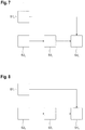
Figure 5 schematically shows a flowchart of a first variant of a method for generating an electrical frequency comb according to the disclosure; -
Figure 6 schematically shows a flowchart of a second variant of a method for generating an electrical frequency comb according to the disclosure; -
Figure 7 schematically shows a flowchart of a third variant of a method for generating an electrical frequency comb according to the disclosure; and -
Figure 8 schematically shows a flowchart of a fourth variant of a method for generating an electrical frequency comb according to the disclosure. - The detailed description set forth below in connection with the appended drawings, where like numerals reference like elements, is intended as a description of various embodiments of the disclosed subject matter and is not intended to represent the only embodiments. Each embodiment described in this disclosure is provided merely as an example or illustration and should not be construed as preferred or advantageous over other embodiments. The illustrative examples provided herein are not intended to be exhaustive or to limit the claimed subject matter to the precise forms disclosed.
- In the following, the term "light" is to be understood to be not restricted to the visible light range, but rather to also include the infrared and ultraviolet frequency ranges.
-
Figures 1 to 4 schematically show different variants of a frequencycomb generating device 10. In all variants, the frequencycomb generating device 10 comprises a pulsed opticallight source 12, alight receiving unit 14, asequence generator 16, and aswitching unit 18. - In
Figures 1 to 4 , dotted lines represent a connection that is signal transmitting in an arbitrary way. This may include wired or wireless communication between the individual device functional units, also called components. Dashed lines represent an optical connection, i.e. light may be transported between the different devices over air, through vacuum and/or via one or several optical fibres. Finally, solid lines represent an electrical wire-based connection. When an arrow is attached to a connecting line, it is to be understood that this arrow depicts the travel direction of a corresponding optical signal or electrical signal, respectively. - The
sequence generator 16 is configured to generate a repeating sequence signal and to forward the repeating sequence signal to theswitching unit 18 to which thesequence generator 16 is connected in a signal transmitting manner. - The repeating sequence may comprise a binary and/or a ternary sequence, which repeats after a predefined time interval, wherein the individual pieces of information are generated with a sequence frequency fS. In other words, the
sequence generator 16 generates pieces of information with a frequency fS , wherein each piece of information may have one of two or one of three values, respectively. - In particular, the repeating sequence may be a pseudorandom binary sequence (PRBS).
- The pulsed optical
light source 12 is configured to generate electromagnetic wave packets, which will be referred to as optical pulses in the following. The pulsed opticallight source 12 generates the optical pulses with a basic pulse frequency fp, which means that the time between two pulses normally is Tp = 1/fp. In particular, the opticallight source 12 is configured to generate short or ultrashort optical pulses, i.e. the width of the individual pulses is much smaller than the time between two pulses even for high frequencies fp. For example, the opticallight source 12 may be an optical pulsed laser. - In time domain, each optical pulse typically has the form of a sinusoid, wherein the maximum amplitude is confined by a Gaussian function. As the individual optical pulses are very short, without restriction of generality each optical pulse will be approximated to have the form of a Dirac function in the following.
- The pulsed optical
light source 12 is synchronized with thesequence generator 16, which means that the pulse frequency fp and the sequence frequency fs have a predefined ratio n = fp /fs. - In a particular embodiment, the ratio n is equal to 1, which means that the optical pulses and the individual pieces of information contained in the repeating sequence signal are generated with the same frequency.
- Moreover, the optical
light source 12 and thesequence generator 16 may be synchronized with respect to phase, which means that there is a predetermined time delay interval between the generation of an optical pulse and a corresponding piece of information contained in the repeating sequence signal. - The
light receiving unit 14 is configured to receive the electromagnetic wave packets, i.e. the optical pulses, and to convert the optical pulses into a corresponding electrical signal. For example, thelight receiving unit 14 is a photo diode. - The functionality of the switching
unit 18 at least partly depends on the embodiment, and will be described in more detail in the following for each embodiment of the frequencycomb generating device 10 with respect toFigures 1 to 4 . - In the embodiment shown in
Figure 1 , the switchingunit 18 is configured to control the pulsed opticallight source 12 based on the repeating sequence signal generated by thesequence generator 16, more specifically based on the current value of the repeating sequence signal. - The switching
unit 18 may be separate from thesequence generator 16 and the pulsed opticallight source 12. Alternatively, the switchingunit 18 may be integrated into thesequence generator 16 or into the pulsed opticallight source 12. - In fact, the pulsed optical
light source 12, thesequence generator 16 and/or theswitching unit 18 may be formed integrally with each other so that the respective components are housed in a common housing. - In this embodiment, an
electrical frequency comb 20 with known characteristics is generated as explained in the following with reference toFigures 1 and5 . - First, the repeating sequence signal is generated via the sequence generator as described above (step S1a).
- The switching
unit 18 controls the pulsed opticallight source 12 to generate an optical pulse every time the current piece of information contained in the repeating sequence signal is equal to at least one of the possible values and to not generate an optical pulse when the current piece of information contained in the repeating sequence signal is equal to one of the other possible values (step S2a). - For example, if the repeating sequence is a binary sequence, the possible individual pieces of information are "0" and "1". In this case, the switching
unit 18 may control the pulsed opticallight source 12 to generate an optical pulse for every "1" and to not generate an optical pulse for every "0" in the binary sequence, or vice versa. - Without any additional control, the pulsed optical
light source 12 would generate optical pulses at a frequency fp which would result in anoptical frequency comb 22 with a spacing of fp of the individual Dirac functions in the frequency domain. - The result of step S2a, however, is a modified optical frequency comb 22' with a spacing between the individual Dirac functions that is much smaller than fp and that has a high signal-to-noise ratio.
- The modified optical frequency comb 22' is then received (step S3a) and converted to the electrical frequency comb 20 (step S4a) via the
light receiving unit 14. - The result of step S4a, i.e. the
electrical frequency comb 20, is characterized by a small spacing between the individual Dirac functions in the frequency domain and by a high signal-to-noise ratio. - In the embodiment shown in
Figure 2 , the switchingunit 18 is an optical switch that is connected to the pulsed opticallight source 12 and to thelight receiving unit 14. The switchingunit 18 is positioned downstream of the pulsed opticallight source 12 and upstream of thelight receiving unit 14. Put it another way, the switchingunit 18 is positioned between the pulsed opticallight source 12 and thelight receiving unit 14. - The switching
unit 18 is configured to attenuate and/or phase shift the optical pulses, also called electromagnetic wave packets, generated by the pulsed opticallight source 12 based on the current value of the repeating sequence signal. - In this embodiment, an
electrical frequency comb 20 with known characteristics is generated as explained in the following with reference toFigures 2 and6 . - First, the repeating sequence signal is generated via the sequence generator as described above (step S1b).
- Moreover, optical pulses are generated via the optical
light source 12 at a frequency fp (step S2b), which results in anoptical frequency comb 22 with a spacing of fp of the individual Dirac functions in the frequency domain. - The switching
unit 18 filters theoptical frequency comb 22 based on the current value of the repeating frequency signal (step S3b). - More precisely, the switching
unit 18 attenuates and/or phase shifts an optical pulse passing theswitching unit 18 every time the current piece of information contained in the repeating sequence signal is equal to at least one of the possible values and does not alter the optical pulse when the current piece of information contained in the repeating sequence signal is equal to one of the other possible values. - For example, if the repeating sequence is a binary sequence, the possible individual pieces of information will be "0" and "1". In this case, the switching
unit 18 may alter the optical pulse for every "1" and may not alter the optical pulse for every "0" in the binary sequence, or vice versa. - In one particular example, the switching
unit 18 completely filters out some of the optical pulses based on the respective value of the repeating sequence signal. - The result of step S3b is a modified optical frequency comb 22' that is equivalent to the one described above in the context of the first possible embodiment.
- Thus, the remaining steps are the same, namely receiving the modified optical frequency comb 22' (step S3b) and converting it to the electrical frequency comb 20 (step S4) via the
light receiving unit 14. - In the embodiment shown in
Figure 3 , the switchingunit 18 is an electrical switch that is connected to thelight receiving unit 14 wherein the switchingunit 18 is located downstream of thelight receiving unit 14. Therefore, electrical signals generated by thelight receiving unit 14 are forwarded to theswitching unit 18. - The switching
unit 18 is configured to attenuate and/or phase shift the electrical pulses generated by thelight receiving unit 14 based on the current value of the repeating sequence signal. - In this embodiment, an
electrical frequency comb 20 with known characteristics is generated as explained in the following with reference toFigures 3 and7 . - First, the repeating sequence signal is generated via the sequence generator as described above (step S1c).
- Moreover, optical pulses are generated via the optical
light source 12 at a frequency fp (step S2c), which results in anoptical frequency comb 22 with a spacing of fp of the individual Dirac functions in the frequency domain. - The
optical frequency comb 22 is converted to a corresponding intermediateelectrical frequency comb 24 by the light receiving unit 14 (step S3c). - The switching
unit 18 filters the intermediateelectrical frequency comb 24 based on the current value of the repeating frequency signal (step S4c). - More precisely, the switching
unit 18 attenuates and/or phase shifts an electrical pulse passing theswitching unit 18 every time the current piece of information contained in the repeating sequence signal is equal to at least one of the possible values and does not alter the electrical pulse when the current piece of information contained in the repeating sequence signal is equal to one of the other possible values. - For example, if the repeating sequence is a binary sequence, the possible individual pieces of information will be "0" and "1". In this case, the switching
unit 18 may alter the electrical pulse for every "1" and may not alter the optical pulse for every "0" in the binary sequence, or vice versa. - In one particular example, the switching
unit 18 completely filters out some of the electrical pulses based on the respective value of the repeating sequence signal. - The result of step S4c is the
electrical frequency comb 20 that is equivalent to the one described in the context of the first embodiment. - In the embodiment shown in
Figure 4 , the switchingunit 18 is configured to control thelight receiving unit 14 based on the repeating sequence signal, more specifically based on the current value of the repeating sequence signal. - The switching
unit 18 may be separate from thesequence generator 16 and thelight receiving unit 14. Alternatively, the switchingunit 18 may be integrated into thesequence generator 16 or into thelight receiving unit 14. - The
light receiving unit 14, thesequence generator 16 and the switchingunit 18 may be placed on a same chip or a same die, also called common chip or rather common die. Hence, a compact frequencycomb generating device 10 is obtained. - In this embodiment, an
electrical frequency comb 20 with known characteristics is generated as explained in the following with reference toFigures 4 and8 . - First, the repeating sequence signal is generated via the
sequence generator 16 as described above (step S1d). - Moreover, optical pulses are generated via the optical
light source 12 at a frequency fp (step S2d), which results in anoptical frequency comb 22 with a spacing of fp of the individual Dirac functions in the frequency domain. - The optical pulses are then received via the light receiving unit 14 (step S3d), wherein the
light receiving unit 14 is controlled by the switchingunit 18 to convert each of the received optical pulses into a corresponding electrical pulse with predefined properties (step S4d), thereby generating theelectrical frequency comb 20. - In step S4d, the predefined properties of each electrical pulse depend on the current value of the repeating sequence signal.
- More precisely, the
light receiving unit 14 generates an electrical pulse every time the current piece of information contained in the repeating sequence signal is equal to at least one of the possible values and does not generate an electrical pulse when the current piece of information contained in the repeating sequence signal is equal to one of the other possible values. - For example, if the repeating sequence is a binary sequence, the possible individual pieces of information will be "0" and "1". In this case, the
light receiving unit 14 may generate an electrical pulse for every "1" and may not generate an electrical pulse for every "0" in the binary sequence, or vice versa. - In another example, if the repeating sequence is a ternary sequence, the individual pieces of information will be "-1", "0" and "1", or at least the actual values can be mapped to these three values.
- In this case, the
light receiving unit 14 may generate a positive voltage electrical pulse for every "1", a negative voltage electrical pulse for every "-1" and may not generate an electrical pulse for every "0" in the ternary sequence. Of course, any other mapping of current values of the repeating sequence signal onto the properties of the electrical pulses is also possible. - In order to generate the positive and negative voltage electrical pulses, the
light receiving unit 14 may comprise afirst conversion element 26 being configured to generate positive voltage electrical pulses and asecond conversion element 28 being configured to generate negative voltage electrical pulses. - The switching
unit 18 may be configured to selectively activate one of the twoconversion elements - Alternatively, the
light receiving unit 14 may comprise acontrol unit 30 being configured to selectively activate theconversion elements unit 18. - As the
control unit 30 is part of thelight receiving unit 14, thecontrol unit 30 may also be located on the same chip or rather the same die. - As described above, the switching
unit 18 may be assigned to different components of the frequencycomb generating device 10 that comprise an optical part and an electrical part which are separated by thelight receiving unit 14. - Hence, the variants shown in
Figures 1 and 2 illustrate that the switchingunit 18 is assigned to the optical part of the frequencycomb generating device 10 whereas theswitching unit 18 is assigned to the electrical part of the frequencycomb generating device 10 in the variant shown inFigure 3 . - The variant according to
Figure 4 illustrates that the switchingunit 18 is assigned to thelight receiving unit 14 itself while controlling thelight receiving unit 14. Thus, the converting properties may be controlled via theswitching unit 18. - Parts of the frequency
comb generating device 10 as shown inFigures 1 and 2 , in particular the pulsed opticallight source 12, thesequence generator 16 and the switchingunit 18, may also be used to only generate the modified optical frequency comb 22', i.e. conversion of the modified optical frequency comb 22' into theelectrical frequency comb 20 may be omitted. - This can be achieved by only performing the steps S1a and S2a as explained above with reference to
Figures 1 and5 or by only performing the steps S1b, S2b and S3b as explained above with reference toFigures 2 and6 . - The resulting modified optical frequency comb 22' in time domain is missing some of its teeth compared to a full optical frequency comb, which translates to a shorter distance between the individual Dirac functions in frequency domain. Thus, by cancelling out some of the Dirac functions in time domain (or rather not generating them in the first place), a fine modified optical frequency comb 22' is achieved.
- The modified optical frequency comb 22' may then be forwarded to further devices, e.g. for the purpose of calibrating said devices.
Claims (15)
- A frequency comb generating device (10) comprising
a pulsed optical light source (12), a sequence generator (16), a light receiving unit (14) and a switching unit (18),
the sequence generator (16) being configured to generate a repeating sequence signal and to forward the repeating sequence signal at least to the switching unit (18),
the pulsed optical light source (12) being configured to generate electromagnetic wave packets, and the pulsed optical light source (12) being synchronized with the sequence generator (16),
the light receiving unit (14) being configured to receive the electromagnetic wave packets, and the light receiving unit (14) being configured to convert the electromagnetic wave packets into an electrical signal,
and the switching unit (18) being configured to at least one of control the pulsed optical light source (12), control the light receiving unit (14), attenuate the electromagnetic wave packets, phase shift the electromagnetic wave packets, attenuate the electrical signal, and phase shift the electrical signal based on the repeating sequence signal. - The frequency comb generating device (10) of claim 1, wherein the sequence generator (16) is configured to generate a pseudorandom binary sequence.
- The frequency comb generating device (10) of claim 1 or 2, wherein the light receiving unit (14) is a photo diode and/or wherein the pulsed optical light source (12) is an optical pulsed laser.
- The frequency comb generating device (10) of any of the preceding claims, wherein the sequence generator (16), the light receiving unit (14) and the switching unit (18) are placed on a same chip or die.
- The frequency comb generating device (10) of any of the preceding claims, wherein the pulsed optical light source (12) and the light receiving unit (14) are optically connected with each other via an optical fibre.
- The frequency comb generating device (10) of any of the preceding claims, wherein the switching unit (18) is configured to control the pulsed optical light source (12) to generate an electromagnetic wave packet for at least one certain current value of the repeating sequence signal and to not generate an electromagnetic wave packet for at least one other certain current value of the repeating sequence signal in particular wherein the switching unit (18) is configured to control the pulsed optical light source (12) to generate an electromagnetic wave packet for each bit of the binary sequence having one value of the two possible values and to not generate an electromagnetic wave packet for each bit having the other value of the two possible values.
- The frequency comb generating device (10) of any of the preceding claims, wherein the switching unit (18) is an electrical switch connected to the light receiving unit (14), the switching unit (18) being positioned downstream of the light receiving unit (14).
- The frequency comb generating device (10) of any of the preceding claims, wherein the switching unit (18) is an optical switch connected to the light receiving unit (14), the switching unit (18) being positioned upstream of the light receiving unit (14).
- The frequency comb generating device (10) of any of the preceding claims, wherein the switching unit (18) is configured to control the light receiving unit (14) to convert the received electromagnetic wave packets into an electrical signal with predefined properties, wherein the predefined properties depend on the current value of the repeating sequence signal.
- The frequency comb generating device (10) of claim 9, wherein the repeating sequence signal comprises a ternary sequence.
- The frequency comb generating device (10) of claim 10, wherein the switching unit (18) is configured to control the light receiving unit (14) to generate a positive voltage pulse, a negative voltage pulse or no voltage pulse based on the current value of the ternary sequence, in particular wherein the light receiving unit (14) is a switchable photo diode comprising two conversion elements (26, 28), the switching unit (18) being configured to selectively activate the conversion elements (26, 28) based on the current value of the ternary sequence.
- The frequency comb generating device (10) of claim 11, wherein the light receiving unit (14) is a switchable photo diode comprising two conversion elements (26, 28) and a control unit (30), wherein the switching unit (18) is configured to forward the repeating sequence signal to the control unit (30), and wherein the control unit (30) is configured to selectively activate the two conversion elements (26, 28) based on the repeating sequence signal.
- A method for generating an optical frequency comb (22), comprising the steps of:- generating a repeating sequence signal; and- generating optical electromagnetic wave packets;wherein parts of the optical electromagnetic wave packets are filtered out based on the repeating sequence signal or the step of generating the electromagnetic wave packets is controlled based on the repeating sequence signal.
- A method for generating an electrical frequency comb, comprising the steps of:- generating a repeating sequence signal;- generating optical electromagnetic wave packets;- receiving the optical electromagnetic wave packets; and- converting the optical electromagnetic wave packets into an electrical signal;wherein parts of the optical electromagnetic wave packets or parts of the electrical signal are filtered out based on the repeating sequence signal, or wherein the step of generating the electromagnetic wave packets is controlled based on the repeating sequence signal or the steps of receiving and converting the optical electromagnetic wave packets are controlled based on the repeating sequence signal.
- The method of claim 13 or 14, wherein the repeating sequence signal comprises a binary or a ternary sequence.
Priority Applications (1)
| Application Number | Priority Date | Filing Date | Title |
|---|---|---|---|
| EP21188257.6A EP3937374A1 (en) | 2018-09-19 | 2019-06-14 | Frequency comb generating device and method for generating a frequency comb |
Applications Claiming Priority (1)
| Application Number | Priority Date | Filing Date | Title |
|---|---|---|---|
| US16/135,808 US10707968B2 (en) | 2018-09-19 | 2018-09-19 | Frequency comb generating device and method for generating a frequency comb |
Related Child Applications (2)
| Application Number | Title | Priority Date | Filing Date |
|---|---|---|---|
| EP21188257.6A Division-Into EP3937374A1 (en) | 2018-09-19 | 2019-06-14 | Frequency comb generating device and method for generating a frequency comb |
| EP21188257.6A Division EP3937374A1 (en) | 2018-09-19 | 2019-06-14 | Frequency comb generating device and method for generating a frequency comb |
Publications (3)
| Publication Number | Publication Date |
|---|---|
| EP3627696A2 true EP3627696A2 (en) | 2020-03-25 |
| EP3627696A3 EP3627696A3 (en) | 2020-11-18 |
| EP3627696B1 EP3627696B1 (en) | 2023-12-27 |
Family
ID=66867061
Family Applications (2)
| Application Number | Title | Priority Date | Filing Date |
|---|---|---|---|
| EP21188257.6A Pending EP3937374A1 (en) | 2018-09-19 | 2019-06-14 | Frequency comb generating device and method for generating a frequency comb |
| EP19180332.9A Active EP3627696B1 (en) | 2018-09-19 | 2019-06-14 | Frequency comb generating device and method for generating a frequency comb |
Family Applications Before (1)
| Application Number | Title | Priority Date | Filing Date |
|---|---|---|---|
| EP21188257.6A Pending EP3937374A1 (en) | 2018-09-19 | 2019-06-14 | Frequency comb generating device and method for generating a frequency comb |
Country Status (3)
| Country | Link |
|---|---|
| US (1) | US10707968B2 (en) |
| EP (2) | EP3937374A1 (en) |
| CN (1) | CN110932058B (en) |
Families Citing this family (2)
| Publication number | Priority date | Publication date | Assignee | Title |
|---|---|---|---|---|
| EP4435508A1 (en) * | 2023-03-22 | 2024-09-25 | Rohde & Schwarz GmbH & Co. KG | Integrated circuit for generating a frequency comb signal, optical system and test and measurement device |
| CN116846479B (en) * | 2023-09-04 | 2023-11-14 | 中山大学 | Dual-optical-frequency comb generation system and method based on communication algorithm |
Family Cites Families (8)
| Publication number | Priority date | Publication date | Assignee | Title |
|---|---|---|---|---|
| US4910458A (en) | 1987-03-24 | 1990-03-20 | Princeton Applied Research Corp. | Electro-optic sampling system with dedicated electro-optic crystal and removable sample carrier |
| US5270643A (en) | 1990-11-28 | 1993-12-14 | Schlumberger Technologies | Pulsed laser photoemission electron-beam probe |
| US7224906B2 (en) * | 2000-09-26 | 2007-05-29 | Celight, Inc. | Method and system for mitigating nonlinear transmission impairments in fiber-optic communications systems |
| US7181097B2 (en) | 2001-03-15 | 2007-02-20 | Massachusetts Institute Of Technology | Methods of achieving optimal communications performance |
| JP4537832B2 (en) | 2004-11-11 | 2010-09-08 | 株式会社東芝 | Optical clock distribution device and optical clock distribution system |
| US7302192B2 (en) * | 2005-04-28 | 2007-11-27 | Menara Networks | Methods of spread-pulse modulation and nonlinear time domain equalization for fiber optic communication channels |
| WO2007099165A2 (en) * | 2006-03-03 | 2007-09-07 | Nokia Siemens Networks Gmbh & Co. Kg | Modulator device for generating an optical transfer signal modulated by means of a binary signal |
| WO2017116383A1 (en) * | 2015-12-28 | 2017-07-06 | Halliburton Energy Services, Inc. | Distributed optical sensing using compressive sampling |
-
2018
- 2018-09-19 US US16/135,808 patent/US10707968B2/en active Active
-
2019
- 2019-06-14 EP EP21188257.6A patent/EP3937374A1/en active Pending
- 2019-06-14 EP EP19180332.9A patent/EP3627696B1/en active Active
- 2019-06-19 CN CN201910530567.2A patent/CN110932058B/en active Active
Also Published As
| Publication number | Publication date |
|---|---|
| CN110932058B (en) | 2024-12-10 |
| US10707968B2 (en) | 2020-07-07 |
| EP3627696B1 (en) | 2023-12-27 |
| US20200092006A1 (en) | 2020-03-19 |
| EP3627696A3 (en) | 2020-11-18 |
| CN110932058A (en) | 2020-03-27 |
| EP3937374A1 (en) | 2022-01-12 |
Similar Documents
| Publication | Publication Date | Title |
|---|---|---|
| US10097338B1 (en) | Isolator with narrow-range clock scrambling unit | |
| RU2007148631A (en) | METHOD AND DEVICE FOR MEASURING THE SPECTRUM OF THE TEMPORARY FORM OF PULSES OF THERAHZ RADIATION | |
| JPH114197A (en) | Optical electric cell with stabilized amplifier | |
| EP3627696B1 (en) | Frequency comb generating device and method for generating a frequency comb | |
| CN102420649A (en) | Optical receiver | |
| FR2494514A1 (en) | DEVICE FOR STABILIZING THE OUTPUT POWER OF A TRANSMITTER MODULE FOR AN OPTICAL FIBER TRANSMISSION SYSTEM | |
| CN110971193A (en) | Millimeter wave noise signal generator based on FP chaotic laser | |
| JP7516592B2 (en) | Photon detection systems and methods | |
| Yang et al. | Illumination sensing in LED lighting systems based on frequency-division multiplexing | |
| JP2019021802A (en) | Optical amplifier control method and optical amplifier | |
| JP2791991B2 (en) | Light switch | |
| US7555218B2 (en) | Optical transceiver having optical receiver with function to cancel noise originated to optical transmitter | |
| US6529674B2 (en) | Optical devices employing an optical thresholder | |
| US10797464B2 (en) | Wavelength locking structure and method for tunable laser | |
| KR20210126604A (en) | Pulsed optical transmitter with improved pulse shape and reduced frequency chirp (CHIRP) | |
| CN101395827B (en) | Modulator device for generating an optical transfer signal modulated by means of a binary signal | |
| US8280262B2 (en) | Light receiving circuit and photocoupler isolation circuit | |
| JP2969854B2 (en) | Chaos generator | |
| US5596449A (en) | Light pulse generator | |
| JPH04221937A (en) | Chaos generator | |
| EP4435508A1 (en) | Integrated circuit for generating a frequency comb signal, optical system and test and measurement device | |
| JP3158634B2 (en) | High-speed small signal current source | |
| JPH09321575A (en) | Attenuator and signal level attenuation method | |
| CN120188385A (en) | AC coupling circuit and transimpedance amplifier | |
| EP0032335A1 (en) | High-power electrical signals generator |
Legal Events
| Date | Code | Title | Description |
|---|---|---|---|
| PUAI | Public reference made under article 153(3) epc to a published international application that has entered the european phase |
Free format text: ORIGINAL CODE: 0009012 |
|
| STAA | Information on the status of an ep patent application or granted ep patent |
Free format text: STATUS: THE APPLICATION HAS BEEN PUBLISHED |
|
| AK | Designated contracting states |
Kind code of ref document: A2 Designated state(s): AL AT BE BG CH CY CZ DE DK EE ES FI FR GB GR HR HU IE IS IT LI LT LU LV MC MK MT NL NO PL PT RO RS SE SI SK SM TR |
|
| AX | Request for extension of the european patent |
Extension state: BA ME |
|
| RIC1 | Information provided on ipc code assigned before grant |
Ipc: G02F 1/35 20060101ALI20200608BHEP Ipc: H04B 10/508 20130101ALI20200608BHEP Ipc: H04B 10/50 20130101ALI20200608BHEP Ipc: H03B 17/00 20060101AFI20200608BHEP |
|
| PUAL | Search report despatched |
Free format text: ORIGINAL CODE: 0009013 |
|
| AK | Designated contracting states |
Kind code of ref document: A3 Designated state(s): AL AT BE BG CH CY CZ DE DK EE ES FI FR GB GR HR HU IE IS IT LI LT LU LV MC MK MT NL NO PL PT RO RS SE SI SK SM TR |
|
| AX | Request for extension of the european patent |
Extension state: BA ME |
|
| RIC1 | Information provided on ipc code assigned before grant |
Ipc: H03B 17/00 20060101AFI20201013BHEP Ipc: G02F 1/35 20060101ALI20201013BHEP Ipc: H04B 10/50 20130101ALI20201013BHEP Ipc: H04B 10/508 20130101ALI20201013BHEP |
|
| STAA | Information on the status of an ep patent application or granted ep patent |
Free format text: STATUS: REQUEST FOR EXAMINATION WAS MADE |
|
| 17P | Request for examination filed |
Effective date: 20210512 |
|
| RBV | Designated contracting states (corrected) |
Designated state(s): AL AT BE BG CH CY CZ DE DK EE ES FI FR GB GR HR HU IE IS IT LI LT LU LV MC MK MT NL NO PL PT RO RS SE SI SK SM TR |
|
| GRAP | Despatch of communication of intention to grant a patent |
Free format text: ORIGINAL CODE: EPIDOSNIGR1 |
|
| STAA | Information on the status of an ep patent application or granted ep patent |
Free format text: STATUS: GRANT OF PATENT IS INTENDED |
|
| INTG | Intention to grant announced |
Effective date: 20230331 |
|
| GRAJ | Information related to disapproval of communication of intention to grant by the applicant or resumption of examination proceedings by the epo deleted |
Free format text: ORIGINAL CODE: EPIDOSDIGR1 |
|
| STAA | Information on the status of an ep patent application or granted ep patent |
Free format text: STATUS: REQUEST FOR EXAMINATION WAS MADE |
|
| INTC | Intention to grant announced (deleted) | ||
| P01 | Opt-out of the competence of the unified patent court (upc) registered |
Effective date: 20230525 |
|
| GRAP | Despatch of communication of intention to grant a patent |
Free format text: ORIGINAL CODE: EPIDOSNIGR1 |
|
| STAA | Information on the status of an ep patent application or granted ep patent |
Free format text: STATUS: GRANT OF PATENT IS INTENDED |
|
| INTG | Intention to grant announced |
Effective date: 20230802 |
|
| GRAS | Grant fee paid |
Free format text: ORIGINAL CODE: EPIDOSNIGR3 |
|
| GRAA | (expected) grant |
Free format text: ORIGINAL CODE: 0009210 |
|
| STAA | Information on the status of an ep patent application or granted ep patent |
Free format text: STATUS: THE PATENT HAS BEEN GRANTED |
|
| RBV | Designated contracting states (corrected) |
Designated state(s): AL AT BE BG CY CZ DE DK EE ES FI FR GB GR HR HU IS IT LT LU LV MC MK MT NL NO PL PT RO RS SE SI SK SM TR |
|
| AK | Designated contracting states |
Kind code of ref document: B1 Designated state(s): AL AT BE BG CY CZ DE DK EE ES FI FR GB GR HR HU IS IT LT LU LV MC MK MT NL NO PL PT RO RS SE SI SK SM TR |
|
| REG | Reference to a national code |
Ref country code: GB Ref legal event code: FG4D |
|
| REG | Reference to a national code |
Ref country code: DE Ref legal event code: R096 Ref document number: 602019043865 Country of ref document: DE |
|
| PG25 | Lapsed in a contracting state [announced via postgrant information from national office to epo] |
Ref country code: GR Free format text: LAPSE BECAUSE OF FAILURE TO SUBMIT A TRANSLATION OF THE DESCRIPTION OR TO PAY THE FEE WITHIN THE PRESCRIBED TIME-LIMIT Effective date: 20240328 |
|
| REG | Reference to a national code |
Ref country code: LT Ref legal event code: MG9D |
|
| PG25 | Lapsed in a contracting state [announced via postgrant information from national office to epo] |
Ref country code: LT Free format text: LAPSE BECAUSE OF FAILURE TO SUBMIT A TRANSLATION OF THE DESCRIPTION OR TO PAY THE FEE WITHIN THE PRESCRIBED TIME-LIMIT Effective date: 20231227 |
|
| PG25 | Lapsed in a contracting state [announced via postgrant information from national office to epo] |
Ref country code: ES Free format text: LAPSE BECAUSE OF FAILURE TO SUBMIT A TRANSLATION OF THE DESCRIPTION OR TO PAY THE FEE WITHIN THE PRESCRIBED TIME-LIMIT Effective date: 20231227 |
|
| PG25 | Lapsed in a contracting state [announced via postgrant information from national office to epo] |
Ref country code: LT Free format text: LAPSE BECAUSE OF FAILURE TO SUBMIT A TRANSLATION OF THE DESCRIPTION OR TO PAY THE FEE WITHIN THE PRESCRIBED TIME-LIMIT Effective date: 20231227 Ref country code: GR Free format text: LAPSE BECAUSE OF FAILURE TO SUBMIT A TRANSLATION OF THE DESCRIPTION OR TO PAY THE FEE WITHIN THE PRESCRIBED TIME-LIMIT Effective date: 20240328 Ref country code: FI Free format text: LAPSE BECAUSE OF FAILURE TO SUBMIT A TRANSLATION OF THE DESCRIPTION OR TO PAY THE FEE WITHIN THE PRESCRIBED TIME-LIMIT Effective date: 20231227 Ref country code: ES Free format text: LAPSE BECAUSE OF FAILURE TO SUBMIT A TRANSLATION OF THE DESCRIPTION OR TO PAY THE FEE WITHIN THE PRESCRIBED TIME-LIMIT Effective date: 20231227 Ref country code: BG Free format text: LAPSE BECAUSE OF FAILURE TO SUBMIT A TRANSLATION OF THE DESCRIPTION OR TO PAY THE FEE WITHIN THE PRESCRIBED TIME-LIMIT Effective date: 20240327 |
|
| REG | Reference to a national code |
Ref country code: NL Ref legal event code: MP Effective date: 20231227 |
|
| REG | Reference to a national code |
Ref country code: AT Ref legal event code: MK05 Ref document number: 1645482 Country of ref document: AT Kind code of ref document: T Effective date: 20231227 |
|
| PG25 | Lapsed in a contracting state [announced via postgrant information from national office to epo] |
Ref country code: NL Free format text: LAPSE BECAUSE OF FAILURE TO SUBMIT A TRANSLATION OF THE DESCRIPTION OR TO PAY THE FEE WITHIN THE PRESCRIBED TIME-LIMIT Effective date: 20231227 |
|
| PG25 | Lapsed in a contracting state [announced via postgrant information from national office to epo] |
Ref country code: SE Free format text: LAPSE BECAUSE OF FAILURE TO SUBMIT A TRANSLATION OF THE DESCRIPTION OR TO PAY THE FEE WITHIN THE PRESCRIBED TIME-LIMIT Effective date: 20231227 Ref country code: RS Free format text: LAPSE BECAUSE OF FAILURE TO SUBMIT A TRANSLATION OF THE DESCRIPTION OR TO PAY THE FEE WITHIN THE PRESCRIBED TIME-LIMIT Effective date: 20231227 Ref country code: NO Free format text: LAPSE BECAUSE OF FAILURE TO SUBMIT A TRANSLATION OF THE DESCRIPTION OR TO PAY THE FEE WITHIN THE PRESCRIBED TIME-LIMIT Effective date: 20240327 Ref country code: NL Free format text: LAPSE BECAUSE OF FAILURE TO SUBMIT A TRANSLATION OF THE DESCRIPTION OR TO PAY THE FEE WITHIN THE PRESCRIBED TIME-LIMIT Effective date: 20231227 Ref country code: LV Free format text: LAPSE BECAUSE OF FAILURE TO SUBMIT A TRANSLATION OF THE DESCRIPTION OR TO PAY THE FEE WITHIN THE PRESCRIBED TIME-LIMIT Effective date: 20231227 Ref country code: HR Free format text: LAPSE BECAUSE OF FAILURE TO SUBMIT A TRANSLATION OF THE DESCRIPTION OR TO PAY THE FEE WITHIN THE PRESCRIBED TIME-LIMIT Effective date: 20231227 |
|
| PG25 | Lapsed in a contracting state [announced via postgrant information from national office to epo] |
Ref country code: IS Free format text: LAPSE BECAUSE OF FAILURE TO SUBMIT A TRANSLATION OF THE DESCRIPTION OR TO PAY THE FEE WITHIN THE PRESCRIBED TIME-LIMIT Effective date: 20240427 |
|
| PG25 | Lapsed in a contracting state [announced via postgrant information from national office to epo] |
Ref country code: AT Free format text: LAPSE BECAUSE OF FAILURE TO SUBMIT A TRANSLATION OF THE DESCRIPTION OR TO PAY THE FEE WITHIN THE PRESCRIBED TIME-LIMIT Effective date: 20231227 Ref country code: CZ Free format text: LAPSE BECAUSE OF FAILURE TO SUBMIT A TRANSLATION OF THE DESCRIPTION OR TO PAY THE FEE WITHIN THE PRESCRIBED TIME-LIMIT Effective date: 20231227 |
|
| PG25 | Lapsed in a contracting state [announced via postgrant information from national office to epo] |
Ref country code: SK Free format text: LAPSE BECAUSE OF FAILURE TO SUBMIT A TRANSLATION OF THE DESCRIPTION OR TO PAY THE FEE WITHIN THE PRESCRIBED TIME-LIMIT Effective date: 20231227 |
|
| PG25 | Lapsed in a contracting state [announced via postgrant information from national office to epo] |
Ref country code: SM Free format text: LAPSE BECAUSE OF FAILURE TO SUBMIT A TRANSLATION OF THE DESCRIPTION OR TO PAY THE FEE WITHIN THE PRESCRIBED TIME-LIMIT Effective date: 20231227 Ref country code: SK Free format text: LAPSE BECAUSE OF FAILURE TO SUBMIT A TRANSLATION OF THE DESCRIPTION OR TO PAY THE FEE WITHIN THE PRESCRIBED TIME-LIMIT Effective date: 20231227 Ref country code: RO Free format text: LAPSE BECAUSE OF FAILURE TO SUBMIT A TRANSLATION OF THE DESCRIPTION OR TO PAY THE FEE WITHIN THE PRESCRIBED TIME-LIMIT Effective date: 20231227 Ref country code: IT Free format text: LAPSE BECAUSE OF FAILURE TO SUBMIT A TRANSLATION OF THE DESCRIPTION OR TO PAY THE FEE WITHIN THE PRESCRIBED TIME-LIMIT Effective date: 20231227 Ref country code: IS Free format text: LAPSE BECAUSE OF FAILURE TO SUBMIT A TRANSLATION OF THE DESCRIPTION OR TO PAY THE FEE WITHIN THE PRESCRIBED TIME-LIMIT Effective date: 20240427 Ref country code: EE Free format text: LAPSE BECAUSE OF FAILURE TO SUBMIT A TRANSLATION OF THE DESCRIPTION OR TO PAY THE FEE WITHIN THE PRESCRIBED TIME-LIMIT Effective date: 20231227 Ref country code: CZ Free format text: LAPSE BECAUSE OF FAILURE TO SUBMIT A TRANSLATION OF THE DESCRIPTION OR TO PAY THE FEE WITHIN THE PRESCRIBED TIME-LIMIT Effective date: 20231227 Ref country code: AT Free format text: LAPSE BECAUSE OF FAILURE TO SUBMIT A TRANSLATION OF THE DESCRIPTION OR TO PAY THE FEE WITHIN THE PRESCRIBED TIME-LIMIT Effective date: 20231227 |
|
| PG25 | Lapsed in a contracting state [announced via postgrant information from national office to epo] |
Ref country code: PL Free format text: LAPSE BECAUSE OF FAILURE TO SUBMIT A TRANSLATION OF THE DESCRIPTION OR TO PAY THE FEE WITHIN THE PRESCRIBED TIME-LIMIT Effective date: 20231227 Ref country code: PT Free format text: LAPSE BECAUSE OF FAILURE TO SUBMIT A TRANSLATION OF THE DESCRIPTION OR TO PAY THE FEE WITHIN THE PRESCRIBED TIME-LIMIT Effective date: 20240429 |
|
| PG25 | Lapsed in a contracting state [announced via postgrant information from national office to epo] |
Ref country code: PT Free format text: LAPSE BECAUSE OF FAILURE TO SUBMIT A TRANSLATION OF THE DESCRIPTION OR TO PAY THE FEE WITHIN THE PRESCRIBED TIME-LIMIT Effective date: 20240429 Ref country code: PL Free format text: LAPSE BECAUSE OF FAILURE TO SUBMIT A TRANSLATION OF THE DESCRIPTION OR TO PAY THE FEE WITHIN THE PRESCRIBED TIME-LIMIT Effective date: 20231227 |
|
| REG | Reference to a national code |
Ref country code: DE Ref legal event code: R097 Ref document number: 602019043865 Country of ref document: DE |
|
| PG25 | Lapsed in a contracting state [announced via postgrant information from national office to epo] |
Ref country code: DK Free format text: LAPSE BECAUSE OF FAILURE TO SUBMIT A TRANSLATION OF THE DESCRIPTION OR TO PAY THE FEE WITHIN THE PRESCRIBED TIME-LIMIT Effective date: 20231227 |
|
| PG25 | Lapsed in a contracting state [announced via postgrant information from national office to epo] |
Ref country code: DK Free format text: LAPSE BECAUSE OF FAILURE TO SUBMIT A TRANSLATION OF THE DESCRIPTION OR TO PAY THE FEE WITHIN THE PRESCRIBED TIME-LIMIT Effective date: 20231227 |
|
| PLBE | No opposition filed within time limit |
Free format text: ORIGINAL CODE: 0009261 |
|
| STAA | Information on the status of an ep patent application or granted ep patent |
Free format text: STATUS: NO OPPOSITION FILED WITHIN TIME LIMIT |
|
| 26N | No opposition filed |
Effective date: 20240930 |
|
| PG25 | Lapsed in a contracting state [announced via postgrant information from national office to epo] |
Ref country code: MC Free format text: LAPSE BECAUSE OF FAILURE TO SUBMIT A TRANSLATION OF THE DESCRIPTION OR TO PAY THE FEE WITHIN THE PRESCRIBED TIME-LIMIT Effective date: 20231227 |
|
| PG25 | Lapsed in a contracting state [announced via postgrant information from national office to epo] |
Ref country code: LU Free format text: LAPSE BECAUSE OF NON-PAYMENT OF DUE FEES Effective date: 20240614 |
|
| PG25 | Lapsed in a contracting state [announced via postgrant information from national office to epo] |
Ref country code: SI Free format text: LAPSE BECAUSE OF FAILURE TO SUBMIT A TRANSLATION OF THE DESCRIPTION OR TO PAY THE FEE WITHIN THE PRESCRIBED TIME-LIMIT Effective date: 20231227 Ref country code: BE Free format text: LAPSE BECAUSE OF NON-PAYMENT OF DUE FEES Effective date: 20240630 |
|
| REG | Reference to a national code |
Ref country code: BE Ref legal event code: MM Effective date: 20240630 |
|
| PG25 | Lapsed in a contracting state [announced via postgrant information from national office to epo] |
Ref country code: CY Free format text: LAPSE BECAUSE OF FAILURE TO SUBMIT A TRANSLATION OF THE DESCRIPTION OR TO PAY THE FEE WITHIN THE PRESCRIBED TIME-LIMIT; INVALID AB INITIO Effective date: 20190614 |
|
| PG25 | Lapsed in a contracting state [announced via postgrant information from national office to epo] |
Ref country code: HU Free format text: LAPSE BECAUSE OF FAILURE TO SUBMIT A TRANSLATION OF THE DESCRIPTION OR TO PAY THE FEE WITHIN THE PRESCRIBED TIME-LIMIT; INVALID AB INITIO Effective date: 20190614 |
|
| PG25 | Lapsed in a contracting state [announced via postgrant information from national office to epo] |
Ref country code: TR Free format text: LAPSE BECAUSE OF FAILURE TO SUBMIT A TRANSLATION OF THE DESCRIPTION OR TO PAY THE FEE WITHIN THE PRESCRIBED TIME-LIMIT Effective date: 20231227 |
|
| PGFP | Annual fee paid to national office [announced via postgrant information from national office to epo] |
Ref country code: GB Payment date: 20260623 Year of fee payment: 8 |
|
| PGFP | Annual fee paid to national office [announced via postgrant information from national office to epo] |
Ref country code: DE Payment date: 20260623 Year of fee payment: 8 |
|
| PGFP | Annual fee paid to national office [announced via postgrant information from national office to epo] |
Ref country code: FR Payment date: 20260622 Year of fee payment: 8 |