EP3627559A1 - A iii-v semiconductor device and a method for forming a iii-v semiconductor device comprising an edge termination structure - Google Patents
A iii-v semiconductor device and a method for forming a iii-v semiconductor device comprising an edge termination structure Download PDFInfo
- Publication number
- EP3627559A1 EP3627559A1 EP18195332.4A EP18195332A EP3627559A1 EP 3627559 A1 EP3627559 A1 EP 3627559A1 EP 18195332 A EP18195332 A EP 18195332A EP 3627559 A1 EP3627559 A1 EP 3627559A1
- Authority
- EP
- European Patent Office
- Prior art keywords
- layer
- forming
- drain contact
- channel
- contact layer
- Prior art date
- Legal status (The legal status is an assumption and is not a legal conclusion. Google has not performed a legal analysis and makes no representation as to the accuracy of the status listed.)
- Granted
Links
Images


Classifications
-
- H—ELECTRICITY
- H10—SEMICONDUCTOR DEVICES; ELECTRIC SOLID-STATE DEVICES NOT OTHERWISE PROVIDED FOR
- H10D—INORGANIC ELECTRIC SEMICONDUCTOR DEVICES
- H10D30/00—Field-effect transistors [FET]
- H10D30/60—Insulated-gate field-effect transistors [IGFET]
- H10D30/64—Double-diffused metal-oxide semiconductor [DMOS] FETs
- H10D30/66—Vertical DMOS [VDMOS] FETs
- H10D30/668—Vertical DMOS [VDMOS] FETs having trench gate electrodes, e.g. UMOS transistors
-
- H—ELECTRICITY
- H10—SEMICONDUCTOR DEVICES; ELECTRIC SOLID-STATE DEVICES NOT OTHERWISE PROVIDED FOR
- H10D—INORGANIC ELECTRIC SEMICONDUCTOR DEVICES
- H10D30/00—Field-effect transistors [FET]
- H10D30/01—Manufacture or treatment
- H10D30/021—Manufacture or treatment of FETs having insulated gates [IGFET]
-
- H—ELECTRICITY
- H10—SEMICONDUCTOR DEVICES; ELECTRIC SOLID-STATE DEVICES NOT OTHERWISE PROVIDED FOR
- H10D—INORGANIC ELECTRIC SEMICONDUCTOR DEVICES
- H10D30/00—Field-effect transistors [FET]
- H10D30/01—Manufacture or treatment
- H10D30/021—Manufacture or treatment of FETs having insulated gates [IGFET]
- H10D30/028—Manufacture or treatment of FETs having insulated gates [IGFET] of double-diffused metal oxide semiconductor [DMOS] FETs
- H10D30/0291—Manufacture or treatment of FETs having insulated gates [IGFET] of double-diffused metal oxide semiconductor [DMOS] FETs of vertical DMOS [VDMOS] FETs
- H10D30/0297—Manufacture or treatment of FETs having insulated gates [IGFET] of double-diffused metal oxide semiconductor [DMOS] FETs of vertical DMOS [VDMOS] FETs using recessing of the gate electrodes, e.g. to form trench gate electrodes
-
- H—ELECTRICITY
- H10—SEMICONDUCTOR DEVICES; ELECTRIC SOLID-STATE DEVICES NOT OTHERWISE PROVIDED FOR
- H10D—INORGANIC ELECTRIC SEMICONDUCTOR DEVICES
- H10D30/00—Field-effect transistors [FET]
- H10D30/60—Insulated-gate field-effect transistors [IGFET]
-
- H—ELECTRICITY
- H10—SEMICONDUCTOR DEVICES; ELECTRIC SOLID-STATE DEVICES NOT OTHERWISE PROVIDED FOR
- H10D—INORGANIC ELECTRIC SEMICONDUCTOR DEVICES
- H10D30/00—Field-effect transistors [FET]
- H10D30/60—Insulated-gate field-effect transistors [IGFET]
- H10D30/64—Double-diffused metal-oxide semiconductor [DMOS] FETs
- H10D30/66—Vertical DMOS [VDMOS] FETs
- H10D30/663—Vertical DMOS [VDMOS] FETs having both source contacts and drain contacts on the same surface, i.e. up-drain VDMOS
-
- H—ELECTRICITY
- H10—SEMICONDUCTOR DEVICES; ELECTRIC SOLID-STATE DEVICES NOT OTHERWISE PROVIDED FOR
- H10D—INORGANIC ELECTRIC SEMICONDUCTOR DEVICES
- H10D30/00—Field-effect transistors [FET]
- H10D30/60—Insulated-gate field-effect transistors [IGFET]
- H10D30/64—Double-diffused metal-oxide semiconductor [DMOS] FETs
- H10D30/66—Vertical DMOS [VDMOS] FETs
- H10D30/665—Vertical DMOS [VDMOS] FETs having edge termination structures
-
- H—ELECTRICITY
- H10—SEMICONDUCTOR DEVICES; ELECTRIC SOLID-STATE DEVICES NOT OTHERWISE PROVIDED FOR
- H10D—INORGANIC ELECTRIC SEMICONDUCTOR DEVICES
- H10D62/00—Semiconductor bodies, or regions thereof, of devices having potential barriers
- H10D62/10—Shapes, relative sizes or dispositions of the regions of the semiconductor bodies; Shapes of the semiconductor bodies
- H10D62/102—Constructional design considerations for preventing surface leakage or controlling electric field concentration
- H10D62/103—Constructional design considerations for preventing surface leakage or controlling electric field concentration for increasing or controlling the breakdown voltage of reverse-biased devices
- H10D62/105—Constructional design considerations for preventing surface leakage or controlling electric field concentration for increasing or controlling the breakdown voltage of reverse-biased devices by having particular doping profiles, shapes or arrangements of PN junctions; by having supplementary regions, e.g. junction termination extension [JTE]
-
- H—ELECTRICITY
- H10—SEMICONDUCTOR DEVICES; ELECTRIC SOLID-STATE DEVICES NOT OTHERWISE PROVIDED FOR
- H10D—INORGANIC ELECTRIC SEMICONDUCTOR DEVICES
- H10D62/00—Semiconductor bodies, or regions thereof, of devices having potential barriers
- H10D62/10—Shapes, relative sizes or dispositions of the regions of the semiconductor bodies; Shapes of the semiconductor bodies
- H10D62/102—Constructional design considerations for preventing surface leakage or controlling electric field concentration
- H10D62/103—Constructional design considerations for preventing surface leakage or controlling electric field concentration for increasing or controlling the breakdown voltage of reverse-biased devices
- H10D62/105—Constructional design considerations for preventing surface leakage or controlling electric field concentration for increasing or controlling the breakdown voltage of reverse-biased devices by having particular doping profiles, shapes or arrangements of PN junctions; by having supplementary regions, e.g. junction termination extension [JTE]
- H10D62/109—Reduced surface field [RESURF] PN junction structures
-
- H—ELECTRICITY
- H10—SEMICONDUCTOR DEVICES; ELECTRIC SOLID-STATE DEVICES NOT OTHERWISE PROVIDED FOR
- H10D—INORGANIC ELECTRIC SEMICONDUCTOR DEVICES
- H10D62/00—Semiconductor bodies, or regions thereof, of devices having potential barriers
- H10D62/10—Shapes, relative sizes or dispositions of the regions of the semiconductor bodies; Shapes of the semiconductor bodies
- H10D62/113—Isolations within a component, i.e. internal isolations
- H10D62/115—Dielectric isolations, e.g. air gaps
- H10D62/116—Dielectric isolations, e.g. air gaps adjoining the input or output regions of field-effect devices, e.g. adjoining source or drain regions
-
- H—ELECTRICITY
- H10—SEMICONDUCTOR DEVICES; ELECTRIC SOLID-STATE DEVICES NOT OTHERWISE PROVIDED FOR
- H10D—INORGANIC ELECTRIC SEMICONDUCTOR DEVICES
- H10D62/00—Semiconductor bodies, or regions thereof, of devices having potential barriers
- H10D62/10—Shapes, relative sizes or dispositions of the regions of the semiconductor bodies; Shapes of the semiconductor bodies
- H10D62/124—Shapes, relative sizes or dispositions of the regions of semiconductor bodies or of junctions between the regions
- H10D62/125—Shapes of junctions between the regions
-
- H—ELECTRICITY
- H10—SEMICONDUCTOR DEVICES; ELECTRIC SOLID-STATE DEVICES NOT OTHERWISE PROVIDED FOR
- H10D—INORGANIC ELECTRIC SEMICONDUCTOR DEVICES
- H10D62/00—Semiconductor bodies, or regions thereof, of devices having potential barriers
- H10D62/10—Shapes, relative sizes or dispositions of the regions of the semiconductor bodies; Shapes of the semiconductor bodies
- H10D62/17—Semiconductor regions connected to electrodes not carrying current to be rectified, amplified or switched, e.g. channel regions
- H10D62/393—Body regions of DMOS transistors or IGBTs
-
- H—ELECTRICITY
- H10—SEMICONDUCTOR DEVICES; ELECTRIC SOLID-STATE DEVICES NOT OTHERWISE PROVIDED FOR
- H10D—INORGANIC ELECTRIC SEMICONDUCTOR DEVICES
- H10D62/00—Semiconductor bodies, or regions thereof, of devices having potential barriers
- H10D62/80—Semiconductor bodies, or regions thereof, of devices having potential barriers characterised by the materials
- H10D62/85—Semiconductor bodies, or regions thereof, of devices having potential barriers characterised by the materials being Group III-V materials, e.g. GaAs
- H10D62/8503—Nitride Group III-V materials, e.g. AlN or GaN
-
- H—ELECTRICITY
- H10—SEMICONDUCTOR DEVICES; ELECTRIC SOLID-STATE DEVICES NOT OTHERWISE PROVIDED FOR
- H10D—INORGANIC ELECTRIC SEMICONDUCTOR DEVICES
- H10D64/00—Electrodes of devices having potential barriers
- H10D64/20—Electrodes characterised by their shapes, relative sizes or dispositions
- H10D64/23—Electrodes carrying the current to be rectified, amplified, oscillated or switched, e.g. sources, drains, anodes or cathodes
- H10D64/251—Source or drain electrodes for field-effect devices
- H10D64/252—Source or drain electrodes for field-effect devices for vertical or pseudo-vertical devices
- H10D64/2527—Source or drain electrodes for field-effect devices for vertical or pseudo-vertical devices for vertical devices wherein the source or drain electrodes are recessed in semiconductor bodies
Definitions
- the present inventive concept relates to a method of forming a III-V semiconductor device comprising an edge termination structure.
- the present inventive concept further relates to a III-V semiconductor device.
- III-V semiconductor devices have progressively replaced traditional Si-based devices for power applications where a high breakdown voltage is required.
- GaN is a promising material for power applications such as vertical channel semiconductor devices.
- the edge termination of such devices typically has a lower breakdown voltage than a parallel-plane structure. This may result into an undesired breakdown of the device edge before the breakdown of the active device part.
- An objective of the present inventive concept is to provide a III-V semiconductor device suitable for power applications and having an edge termination structure enabling an improved breakdown voltage. Further or alternative objectives may be understood from the following description.
- a III-V semiconductor device comprising:
- III-V semiconductor device comprising:
- the present inventive concept is based on the insight that an increased breakdown voltage may be achieved at an edge termination structure by providing a RESURF layer as part of the layer stack forming the active layers of the III-V semiconductor device.
- the RESURF layer enables a reduced peak electrical field at the junction between the first conductivity type drain contact and drift layers and the second conductivity type channel and body contact layers. More specifically, the RESURF layer enables a spreading out of the electrostatic potential along the length of the edge termination structure.
- the channel layer has a double function of supporting one or more vertical channels of the semiconductor device and providing the RESURF layer at the edge termination structure. This also enables the RESURF dose to be conveniently tuned via the doping concentration of the channel layer and the vertical dimension of the insulating region.
- a thickness and doping level of the channel layer will influence the threshold voltage VT of the device. Accordingly, the doping level of the channel layer can be adjusted to a specific target VT, wherein a thickness of the remaining thickness portion RESURF layer may be set to obtain the desired RESURF effect, i.e. to obtain the RESURF dose in the RESURF layer. This may facilitate the device design.
- the device structure allows forming of a vertical channel device, more specifically a metal-oxide-semiconductor field-effect-transistor (MOSFET) comprising a set of (one or more) vertically oriented channels.
- MOSFET metal-oxide-semiconductor field-effect-transistor
- a channel may be defined to extend vertically through the channel layer, along a gate electrode.
- the drain contact may be configured as a common drain electrode for the semiconductor device, i.e. common to each of the plural vertical channel devices.
- the channel layer may be epitaxially grown on the drift layer and the body contact layer may be epitaxially grown on the channel layer.
- the channel layer and body contact layer may thus form epitaxial layers.
- the channel layer and the body contact layer may further be in-situ doped to form layers of the second conductivity type. This allows the channel and body contact layers to be formed with an advantageous degree of control and doped to a respective desired level in a manner reducing the amount of defects and damages, compared to doping by for instance ion implantation.
- each one of the layers of the layer stack may be epitaxillay grown and, optionally, in-situ doped to provide the respective first and the second conductivity type.
- a doping concentration of the body contact layer may be greater than a doping concentration of the channel layer. Thereby a good electric contact may be achieved between the body contact layer and a body contact. Meanwhile, a lower doping concentration may be provided in the channel layer and thus the RESURF layer. A comparably lower doping concentration in the channel layer enables a desired RESURF does to be obtained at a greater thickness.
- the channel layer may comprise GaN.
- a GaN-based semiconductor device may be formed.
- GaN has several properties which makes it advantageous to use in semiconductor device, notably power applications but also in radio frequency and analog applications.
- each one of the layers of the layer stack may comprise GaN.
- Each one of the layers of the layer stack may be GaN-layers (i.e. doped or undoped as appropriate).
- the first conductivity type may be an n-type and the second conductivity type may be a p-type.
- the drain contact layer may be an n-type layer
- the drift layer may be an n-type layer
- the channel layer may be a p-type layer
- the body contact layer may be a p-type layer
- the source contact layer may be an n-type layer.
- an n-type semiconductor device may be provided, preferably an n-type GaN.
- an n-type semiconductor device may be advantageous for high-voltage operation, it is in principle possible to form a p-type semiconductor device, e.g.
- the drain contact layer may be a p-type layer
- the drift layer may be a p-type layer
- the channel layer may be an n-type layer
- the body contact layer may be an n-type layer
- the source contact layer may be a p-type layer.
- a dopant dose of the RESURF layer falls within a range of 1 E13 at/cm 2 to 3E13 at/cm 2 .
- a dopant dose in this range may provide a RESURF effect which contributes appreciably to an improved break down voltage.
- a doping concentration of the channel layer and a thickness of the remaining thickness portion below the insulating region should be such that a dopant dose within a range of 1E13 at/cm 2 to 3E13 at/cm 2 is obtained in the RESURF layer
- a length dimension of the insulating region may be formed to be greater than a thickness dimension of the drift layer. This may ensure that breakdown does not occur prematurely.
- Forming of the edge termination structure may comprise etching a trench through the layer stack and stopping the etching within the channel layer, thereby forming the trench with said thickness portion of the channel layer remaining under the bottom of the trench. Subsequently, an insulating material may be deposited in the trench.
- the RESURF layer may be formed, using reliable and comparably simple processing.
- the etching may comprise etching (in a top-down direction), through the source contact layer, the body contact layer and into the channel layer until a thickness portion of the channel layer remains under the bottom of the trench. The etching may be stopped at a position such that a desired RESURF dose of the RESURF layer is obtained.
- the drain contact may be arranged or formed adjacent to the insulating region of the edge termination structure.
- Forming of the drain contact may comprise:
- the drain contact trench is advantageously formed to extend partially into the drain contact layer, to enable a good electrical connection between the drain contact and the drain contact layer.
- the drain contact may be formed either prior to or subsequent to forming the insulating region. If an insulating region comprising a trench is formed prior to the drain contact, the trench may advantageously be filled prior to drain contact trench formation, among others to simplify masking operations.
- a drain contact insulating layer may be formed in the drain contact trench prior to filling the drain contact trench with the conductive contact material. Thereafter the drain contact may be formed.
- An insulating layer may hence be formed between vertical sidewalls of the drain contact and the layers of the layer stack through which the drain contact extends.
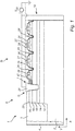
- Figure 1 With reference to Figure 1 there is shown, in cross-section, a semiconductor device 1.
- Figure 2 shows an enlarged view of an inner edge region (denoted "I") of the semiconductor device 1.
- the structure may extend laterally or horizontally beyond the illustrated section.
- the illustrated planes of section extending through the structure are common to all the figures unless stated otherwise.
- the relative dimensions of the shown elements, in particular the relative thickness of the layers is merely schematic and may, for the purpose of illustrational clarity, differ from a physical structure.
- directions X and Y indicates a horizontal direction and a vertical direction, respectively.
- the device 1 comprises a III-V semiconductor layer stack 10.
- the layer stack 10 comprises in a bottom-up direction (i.e. being parallel to the vertical direction Y): a drain contact layer 14, a drift layer 16, a channel layer 18, a body contact layer 19 (visible in Figure 2 ) and a source contact layer 20.
- the drift layer 16 is formed on the drain contact layer 14.
- the channel layer 18 is formed on the drift layer 16.
- the body contact layer 19 is formed on the channel layer 18.
- the source contact layer 20 is formed on the body contact layer 19.
- the layer stack 10 may be formed as an epitaxial layer stack wherein each one of the layers of the layer stack 10 may be formed as a respective epitaxial layer.
- Each one of the layers of the layer stack 10 may be formed by a III-V semiconductor material, for instance GaN or AlGaN.
- GaN-layers may provide better channel and mobility properties than AlGaN-layers, which may be preferable in some applications.
- AlGaN-layers on the other hand may provide an even higher critical electrical field than GaN-layers, which may be preferable in some applications. If the layers of the layer stack 10 are formed of AlGaN, the layers may advantageously have the same Al-concentration, to counteract formation of polarization charges.
- the drain contact layer 14, the drift layer 16 and the source contact layer 20 may be doped to form layers of an n-type conductivity and the channel layer 18 and the body contact layer 19 may be doped to form layers of a p-type conductivity, or vice versa.
- the drain contact layer 14 may be formed by an n + or n ++ GaN layer
- the drift layer 16 may be formed by an n - GaN layer
- the channel layer 18 (and consequently also the thickness portion 18a discussed below) may be formed by a p GaN layer
- the body contact layer 19 may be formed by a p + GaN layer
- the source contact layer may be formed by an n + or n ++ GaN layer.
- an n + or n ++ layer may have a doping concentration in the range of 5E19 to 5E20 cm -3 (i.e. 5*10 19 to 5*10 20 ).
- An n - layer may have a doping concentration in the range of 1E14 to 1E17 cm -3 .
- a p or p+ layer may have a doping concentration in the range of 5E16 to 5E18 cm -3 .
- a first diode junction i.e. an np- or pn-junction
- a second diode junction i.e. a pn- or np-junction
- the layer stack 10 is formed on a substrate 2.
- the substrate may be a semiconductor substrate, such as a silicon substrate.
- the substrate 2 may be a silicon (Si) substrate having a ⁇ 111> upper surface.
- a Si ⁇ 111> surface allows forming the layer stack 10 as a stack of epitaxially grown III-V layers, especially GaN-based layers.
- a buffer layer structure 12 may be formed on the substrate 2.
- the drain contact layer 14 may be formed on the buffer layer structure 12.
- the buffer layer structure 12 may be formed in a manner which per se is known in the art to provide stress relief between the substrate 2 and the layer stack 10.
- the device 1 comprises a set of gate structures 24.
- the section of the device 1 visible in Figure 1 shows three gate structures, and part of a fourth gate structure, commonly referenced 24. However, the device 1 may comprise both a smaller and greater number of gate structures.
- the set of gate structures 14 may even include only a single gate electrode.
- Each one of the one or more gate structures 24 of the set of gate structures extends through the source contact layer 20, the body contact layer 19 and the channel layer 18.
- a vertically oriented MOSFET channel may accordingly be defined in the channel layer 18, along each gate structure 24.
- the channel may extend between the drift layer 16, through the channel layer 18 and the body contact layer 19, and the source contact layer 20. Since each gate structure 24 extends through the channel layer 18, a vertically oriented channel may be defined on either side of each gate structure 24.
- Each gate structure 24 may comprise a gate electrode 24e and a gate dielectric 24i.
- a gate electrode 24e may be formed by a conventional gate material, for instance Ti or TiAl, or as a stack of layers, for instance a stack comprising TiN, Ti, Al.
- the gate electrode 24e may also comprise a conductive fill material such as W.
- the gate dielectric 24i may be of a conventional type, such as Al 2 O 3 , SiO 2 or Si 3 N 4 , or combinations thereof.
- Each gate structure 24 may be formed in a respective gate trench formed in the layer stack 10 wherein the gate electrode 24e and the gate dielectric 24i may extend vertically through the channel layer 18.
- the gate electrode 24e may be laterally coupled (i.e. a capacitive coupling) to the channel layer 18, on either side of the gate structure 24.
- the device 1 comprises a set of source contacts 26.
- the device 1 comprises a set of body contacts 27.
- the number of source contacts 26 and the number of body contacts 27 may correspond to the number of vertical channels formed along the gate structures 24.
- Each one of the one or more source contacts 26 is arranged to contact the source contact layer 20.
- Each one of the one or more body contacts 27 is arranged to contact the body contact layer 19.
- Each body contact may extend through the source contact layer 20 and into the body contact layer 19.
- the source contacts 26 and the body contacts 27 may be formed by a conventional contact material, such as Ti and/or Al.
- each body contact 27 may be electrically shorted to an adjacent source contact 26.
- the source contacts 26/the source contact layer 20 and the body contact 27/the body contact layer 19 may be on the same potential.
- the gate electrodes 24e may be shorted to the body contacts 27.
- these electrical configurations are merely optional and it is generally also possible to form the source and body contacts 26, 27 and gate electrodes 24e as electrically separate contacts.
- the device 1 further comprises an edge termination structure comprising a drain contact 28.
- the drain contact 28 extends vertically through the layer stack 10 and contacts the drain contact layer 14.
- the drain contact layer 14 extends below each of the gate electrodes 24, and source/body contacts 26/27. Accordingly, the drain contact 28 may form a common drain contact 28 for each of the vertical channels extending through the channel layer 18.
- the drain contact 28 may be arranged in a drain contact trench extending through the layer stack 10 and to, optionally partly into, the drain contact layer 14.
- the drain contact 28 may be insulated, laterally, from the layer stack 10 by a drain contact insulating layer 29, arranged along a sidewall of the drain contact 28.
- the gate electrodes 24, as well as the source, drain and body contacts 26, 27, 28 may protrude above an insulating layer 22 formed above the layer stack 10, thereby providing electrical access to the contacts.
- the insulating layer 22 may for instance be formed by a conventional interlayer dielectric (ILD) material, such as an oxide layer.
- ILD interlayer dielectric
- the contacts 26, 27, 28 as well as the gate structures 24 are shown to present a tapered shape. This however merely represents an example and it is also possible to form one or more of the contacts 26, 27, 28 and gate structures 24 with vertically oriented/perpendicular sidewalls.
- the drain contact 28 may be arranged in a peripheral region or edge region "E" of the device 1/substrate 2.
- the edge region “E” may comprise a saw lane 4, which forms the outermost periphery of the device 1.
- the edge region “E” may further comprise an outer isolation region 6, laterally separating the layer stack 10 from the saw lane 4.
- the drain contact 28 has an outer edge "O” facing outwardly towards the outermost periphery.
- the drain contact 28 has an opposite inner edge "I” facing inwardly towards a central region "D" of the device 1/substrate 2, i.e. away from the outermost periphery.
- the central region “D” may also be referred to as the active device region “D”.
- the gate structures 24, the source contacts 26 and the body contacts 27 may be formed in the region "D".
- the edge termination structure further comprises an insulating region in the form of a trench 30 filled with an insulating material 32, such as a silicon oxide, a combination of materials such as SiO 2 /Si 3 N 4 or Al 2 O 3 /SiO 2 , or some other dielectric material.
- an insulating material 32 such as a silicon oxide, a combination of materials such as SiO 2 /Si 3 N 4 or Al 2 O 3 /SiO 2 , or some other dielectric material.
- the trench 30 extends vertically through the layer stack 10, into the channel layer 18 such that a thickness portion 18a of the channel layer 18 remains under a bottom of the trench 30.
- the remaining thickness portion 18a of the channel layer 18 forms a reduced surface field, RESURF, layer (which also will be referenced 18a).
- the trench 30 is formed adjacent to the drain contact 28, and extends along the inner edge "I" thereof.
- a length dimension L of the trench 30 i.e.
- an insulating region may also be formed through ion implantation into a region of the layer stack 10, the region having an extension corresponding to that of the trench 30.
- the RESURF layer 18a enables a reduced peak electrical field at the junction between the n/p type drain contact and drift layers 14, 16 and the p/n type channel and body contact layers 18, 19.
- the RESURF dose (i.e. at/cm2) is determined by the product of the thickness of the RESURF layer 18a and the doping level of the RESURF layer 18a. For instance, for a thickness T and a doping concentration C, the RESURF dose will be T ⁇ C. Meanwhile, a thickness and doping level of the channel layer 18 will influence the threshold voltage VT of the device.
- the doping level of the channel layer 18 can during device design be adjusted to a specific target VT, wherein the thickness T of the remaining thickness portion/RESURF layer 18a may be set to obtain the desired RESURF effect.
- the doping concentration of the channel layer 18 and the thickness of the remaining thickness portion 18a may be set such that a dopant dose of the RESURF layer (i.e. the RESURF dose) may fall within a range of 1E13 at/cm 2 to 3E13 at/cm 2 .
- a dopant dose in this range may provide a RESURF effect which contributes appreciably to an improved break down voltage.
- the RESURF layer may be formed with a thickness in the range of 100-600 nm.
- a GaN RESURF layer 18a the RESURF dose may advantageously be 1.8E13 at/cm 2 , at least within ⁇ 10%, more preferably within ⁇ 5%, even more preferably within ⁇ 2%.
- Figures 3a-b depict the same region as Figure 2 .
- the III-V semiconductor layer stack 10 has been formed.
- the drain contact layer 14 may be epitaxially grown on an upper surface of the buffer layer structure 12.
- the drift layer 16 may be epitaxially grown on an upper surface of the drain contact layer 16.
- the channel layer 18 may be epitaxially grown on an upper surface of the drift layer 16.
- the body contact layer 19 may be epitaxially grown on the channel layer 18.
- the source contact layer 20 may be epitaxially grown on the body contact layer 19.
- the layers of the layer stack 10 may for instance be formed by metal organic chemical vapor deposition (MOCVD).
- MOCVD metal organic chemical vapor deposition
- Each one of the layers may be in-situ doped by introducing suitable impurities (in accordance with the intended conductivity type) in the growth reactor during the epitaxial growth. Doping by ion implantation is also possible, however advantageously at least the channel layer 18 and the body contact layer 19 are in-situ doped to avoid defect formation.
- the trench 30 of the edge termination structure has been formed and subsequently filled with the insulating material 32.
- the trench 30 may be formed by etching through the layers of the layer stack 10. The etching may be stopped within the channel layer 18, thereby forming the trench with the thickness portion 18a of thickness T remaining under the bottom of the trench 30. As discussed above in connection with Figures 1 and 2 the remaining thickness portion 18a forms the RESURF layer 18a.
- the trench formation 30 may comprise forming of an etch mask above the layer stack 10, the etch mask having an opening defining the horizontal dimensions of the trench 30. The trench 30 may thereafter be formed by etching the layer stack 10 through the opening in the etch mask.
- the etch mask may be of a conventional type, for instance an etch mask comprising a lithographically patterned photoresist layer. Any conventional dry or wet etching processes, suitable for etching III-V semiconductor materials may be used, for instance a dry plasma etching process.
- the etching of the layer stack 10 may result in formation of a trench 30 with an inclined sidewall. This may however be dependent on the actual etch process used and it may also be possible to obtain a trench 30 with a vertically oriented/perpendicular sidewall.
- the insulating material 32 may be deposited to fill the trench 30.
- the insulating material 32 may for instance be a silicon oxide or some other dielectric material.
- the insulating material 32 may be deposited using a conventional deposition process, such as chemical vapor deposition (CVD). Insulating material deposited outside of the trench 32 may be removed by for instance etching back the insulating material 32 until an upper surface of the source contact layer 20 is exposed.
- CVD chemical vapor deposition
- an insulating region may be formed through subjecting the layer stack 10 to an ion implantation process.
- the ion implantation process for instance implanting N, Ar or He
- the ion implantation process may be configured to produce an implanted insulating region of damaged crystallographic structure of the layers of the layer stack 10. Similar to the trench 30 and insulating material 32, the damaged region, may extend partly into the channel layer 18 such that an undamaged thickness portion 18a (i.e. the RESURF layer) of the channel layer 18 remains under the insulating region.
- a drain contact trench 34 may be formed adjacent to the trench 30.
- the drain contact trench 34 may be formed by etching the layer stack 10 in a region adjacent to the trench 30.
- the drain contact trench may be formed to extend 34 vertically through the layer stack 10 to expose the drain contact layer 14, as shown optionally partly into the drain contact layer 14.
- the drain contact trench formation may comprise forming of an etch mask above the layer stack 10, the etch mask having an opening defining the horizontal dimensions of the trench 34.
- the drain contact trench 34 may thereafter be formed by etching the layer stack 10 through the opening in the etch mask.
- the etch mask may be of a conventional type, for instance an etch mask comprising a lithographically patterned photoresist layer. For instance, a same etching process as used during the formation of the trench 30 may be used.
- the drain contact 28 may be formed by filling the drain contact trench 34 with a conductive contact material.
- a drain contact insulating layer 29 may be deposited in the drain contact trench 34 prior to depositing the conductive contact material.
- the drain contact insulating layer 29 may be formed by depositing a conformal insulating layer using atomic layer deposition (ALD), for instance an ALD oxide or a low-k ALD dielectric.
- ALD atomic layer deposition
- the conformal layer may subsequently be etched such that a conformal insulating layer remains only on the sidewall of the drain contact trench 29.
- an oxide or other low-k dielectric may be deposited by CVD and subsequently etched such that an insulating layer 29 remains only on the sidewall of the drain contact trench 34.
- the set of gate structures 24, the set of source contacts 26 and the set drain contacts 27 may be formed in a corresponding manner to arrive at the device 1 shown in Figures 1 and 2 .
- Respective trenches for the sets of contacts 26, 27 and the set of gate structures 24 may be formed in the layer stack 10.
- the set of source contact trenches may be etched to expose the source contact layer 20.
- the set of body contact trenches may be etched to expose the body contact layer 19.
- the contact trenches may subsequently be filled with a conductive contact material, possibly preceded by a forming of an insulating layer on sidewalls of the contact trenches.
- the etching of the contact trenches for the drain contact 28, the set of source contacts 26 and the set of body contacts 27 may be formed in sequential patterning processes.
- Conductive contact material may thereafter be deposited to form a conductive material layer covering the layer stack 10 and filling the contact trenches holes.
- the conductive material layer may subsequently be patterned to form the drain contact 28, the source contacts 26 and the body contacts 27. It is however also possible to form the contacts 26, 27 and 28 sequentially, in separate etching and deposition processes.
- Respective gate trenches for the set of gate structures 24 may be formed in the layer stack 10, advantageously prior to forming the contacts 26, 27, 28.
- the set of gate trenches may be etched to extend through the channel layer 18, and optionally partly into the drift layer 16.
- the gate structures 24 may thereafter be formed by first depositing the gate dielectric layer 24i and thereafter depositing conductive gate material for the gate electrodes 24.
- the layer stack 10 may be covered by the insulating layer 22 prior to forming the set of gate structures 24, the set of source contacts 26 and the set drain contacts 27, and optionally also prior to forming the trench 30.
- the respective trenches may comprise etching through also the insulating layer 22.
- the insulating layer 22 may be formed after trench and gate/contact formation. Electrical access to the gates and contacts may then be provided by etching openings in the insulating layer 22 above the gate structures 24 and source and body contacts 26, 27 forming vertical via connections therein.
- the formation and filling of the trench 30 is occurs prior to forming the drain contact trench 34.
- the gate structures 24, the set of source contacts 26 and the set of body contacts 27 may be formed in any mutual order, and either before or after forming and filling the trench 30.
Landscapes
- Insulated Gate Type Field-Effect Transistor (AREA)
- Thin Film Transistor (AREA)
Abstract
Description
- The present inventive concept relates to a method of forming a III-V semiconductor device comprising an edge termination structure. The present inventive concept further relates to a III-V semiconductor device.
- Over the last decades, III-V semiconductor devices have progressively replaced traditional Si-based devices for power applications where a high breakdown voltage is required. For instance, GaN is a promising material for power applications such as vertical channel semiconductor devices. However, the edge termination of such devices typically has a lower breakdown voltage than a parallel-plane structure. This may result into an undesired breakdown of the device edge before the breakdown of the active device part.
- An objective of the present inventive concept is to provide a III-V semiconductor device suitable for power applications and having an edge termination structure enabling an improved breakdown voltage. Further or alternative objectives may be understood from the following description.
- According to a first aspect of the present inventive concept there is provided a method for forming a III-V semiconductor device comprising:
- forming a III-V semiconductor layer stack comprising in a bottom-up direction: a drain contact layer, a drift layer, a channel layer, a body contact layer and a source contact layer, wherein the drain contact layer, the drift layer and the source contact layer have a first conductivity type and the channel layer and the body contact layer have a second conductivity type opposite the first conductivity type,
- forming a set of gate structures extending through the source contact layer, the body contact layer and the channel layer,
- forming a set of source contacts contacting the source contact layer, and
- forming an edge termination structure, wherein forming the edge termination structure comprises:
- forming a drain contact extending through the layer stack and contacting the drain contact layer, and
- forming an insulating region extending vertically through the layer stack, into the channel layer such that a thickness portion of the channel layer remains under a bottom of the insulating region, wherein the remaining thickness portion of the channel layer forms a reduced surface field, RESURF, layer.
- According to a second aspect there is provided III-V semiconductor device comprising:
- a III-V semiconductor layer stack comprising in a bottom-up direction: a drain contact layer, a drift layer, a channel layer, a body contact layer and a source contact layer, wherein the drain contact layer, the drift layer and the source contact layer have a first conductivity type and the channel layer and the body contact layer have a second conductivity type opposite the first conductivity type,
- a set of gate structures extending through the source contact layer, the body contact layer and the channel layer,
- a set of source contacts contacting the source contact layer, and
- an edge termination structure comprising:
- a drain contact extending through the layer stack and contacting the drain contact layer, and
- an insulating region extending vertically through the layer stack, into the channel layer such that a thickness portion of the channel layer remains under a bottom of the insulating region, wherein the remaining thickness portion of the channel layer forms a reduced surface field, RESURF, layer.
- The present inventive concept is based on the insight that an increased breakdown voltage may be achieved at an edge termination structure by providing a RESURF layer as part of the layer stack forming the active layers of the III-V semiconductor device.
- According to the Reduced Surface Field (RESURF) effect a surface field at an isolation junction is decreased through 2-D depletion. According to the first and second inventive aspects, the RESURF layer enables a reduced peak electrical field at the junction between the first conductivity type drain contact and drift layers and the second conductivity type channel and body contact layers. More specifically, the RESURF layer enables a spreading out of the electrostatic potential along the length of the edge termination structure.
- As the RESURF layer is formed by a thickness portion of the channel layer, the channel layer has a double function of supporting one or more vertical channels of the semiconductor device and providing the RESURF layer at the edge termination structure. This also enables the RESURF dose to be conveniently tuned via the doping concentration of the channel layer and the vertical dimension of the insulating region. A thickness and doping level of the channel layer will influence the threshold voltage VT of the device. Accordingly, the doping level of the channel layer can be adjusted to a specific target VT, wherein a thickness of the remaining thickness portion RESURF layer may be set to obtain the desired RESURF effect, i.e. to obtain the RESURF dose in the RESURF layer. This may facilitate the device design.
- By the configuration of the drain contact layer, drift layer, channel layer, body contact layer and source contact layer in a layer stack, the device structure allows forming of a vertical channel device, more specifically a metal-oxide-semiconductor field-effect-transistor (MOSFET) comprising a set of (one or more) vertically oriented channels. A channel may be defined to extend vertically through the channel layer, along a gate electrode.
- By providing a plurality of gate structures and a plurality of source electrodes, a plurality of vertical channels may be formed. Accordingly, the drain contact may be configured as a common drain electrode for the semiconductor device, i.e. common to each of the plural vertical channel devices.
- The channel layer may be epitaxially grown on the drift layer and the body contact layer may be epitaxially grown on the channel layer. The channel layer and body contact layer may thus form epitaxial layers. The channel layer and the body contact layer may further be in-situ doped to form layers of the second conductivity type. This allows the channel and body contact layers to be formed with an advantageous degree of control and doped to a respective desired level in a manner reducing the amount of defects and damages, compared to doping by for instance ion implantation.
- Advantageously, each one of the layers of the layer stack may be epitaxillay grown and, optionally, in-situ doped to provide the respective first and the second conductivity type.
- A doping concentration of the body contact layer may be greater than a doping concentration of the channel layer. Thereby a good electric contact may be achieved between the body contact layer and a body contact. Meanwhile, a lower doping concentration may be provided in the channel layer and thus the RESURF layer. A comparably lower doping concentration in the channel layer enables a desired RESURF does to be obtained at a greater thickness.
- The channel layer may comprise GaN. Thereby a GaN-based semiconductor device may be formed. GaN has several properties which makes it advantageous to use in semiconductor device, notably power applications but also in radio frequency and analog applications. Advantageously, each one of the layers of the layer stack may comprise GaN. Each one of the layers of the layer stack may be GaN-layers (i.e. doped or undoped as appropriate).
- The first conductivity type may be an n-type and the second conductivity type may be a p-type. Accordingly, the drain contact layer may be an n-type layer, the drift layer may be an n-type layer, the channel layer may be a p-type layer, the body contact layer may be a p-type layer and the source contact layer may be an n-type layer. Thereby, an n-type semiconductor device may be provided, preferably an n-type GaN. Although an n-type semiconductor device may be advantageous for high-voltage operation, it is in principle possible to form a p-type semiconductor device, e.g. a p-type GaN wherein the drain contact layer may be a p-type layer, the drift layer may be a p-type layer, the channel layer may be an n-type layer, the body contact layer may be an n-type layer and the source contact layer may be a p-type layer.
- A dopant dose of the RESURF layer falls within a range of 1 E13 at/cm2 to 3E13 at/cm2. A dopant dose in this range may provide a RESURF effect which contributes appreciably to an improved break down voltage. In other words, a doping concentration of the channel layer and a thickness of the remaining thickness portion below the insulating region should be such that a dopant dose within a range of 1E13 at/cm2 to 3E13 at/cm2 is obtained in the RESURF layer
- A length dimension of the insulating region may be formed to be greater than a thickness dimension of the drift layer. This may ensure that breakdown does not occur prematurely.
- Forming of the edge termination structure may comprise etching a trench through the layer stack and stopping the etching within the channel layer, thereby forming the trench with said thickness portion of the channel layer remaining under the bottom of the trench. Subsequently, an insulating material may be deposited in the trench. Thus, the RESURF layer may be formed, using reliable and comparably simple processing. The etching may comprise etching (in a top-down direction), through the source contact layer, the body contact layer and into the channel layer until a thickness portion of the channel layer remains under the bottom of the trench. The etching may be stopped at a position such that a desired RESURF dose of the RESURF layer is obtained.
- The drain contact may be arranged or formed adjacent to the insulating region of the edge termination structure.
- Forming of the drain contact may comprise:
- etching a drain contact trench by etching the layer stack in a region adjacent to the insulating region, the drain contact trench extending vertically through the layer stack to expose the drain contact layer, and
- forming the drain contact by filling the drain contact trench with a conductive contact material.
- The drain contact trench is advantageously formed to extend partially into the drain contact layer, to enable a good electrical connection between the drain contact and the drain contact layer.
- The drain contact may be formed either prior to or subsequent to forming the insulating region. If an insulating region comprising a trench is formed prior to the drain contact, the trench may advantageously be filled prior to drain contact trench formation, among others to simplify masking operations.
- A drain contact insulating layer may be formed in the drain contact trench prior to filling the drain contact trench with the conductive contact material. Thereafter the drain contact may be formed. An insulating layer may hence be formed between vertical sidewalls of the drain contact and the layers of the layer stack through which the drain contact extends.
- The above, as well as additional objects, features and advantages of the present inventive concept, will be better understood through the following illustrative and non-limiting detailed description, with reference to the appended drawings. In the drawings like reference numerals will be used for like elements unless stated otherwise.
-
Fig. 1 is schematic overview of a semiconductor device. -
Fig. 2 is an enlarged view of the device ofFigure 1 . -
Figs 3a-3b schematically illustrate a method for forming a semiconductor device - With reference to
Figure 1 there is shown, in cross-section, a semiconductor device 1.Figure 2 shows an enlarged view of an inner edge region (denoted "I") of the semiconductor device 1. The structure may extend laterally or horizontally beyond the illustrated section. The illustrated planes of section extending through the structure are common to all the figures unless stated otherwise. It is noted that the relative dimensions of the shown elements, in particular the relative thickness of the layers, is merely schematic and may, for the purpose of illustrational clarity, differ from a physical structure. InFigure 1 , directions X and Y indicates a horizontal direction and a vertical direction, respectively. - The device 1 comprises a III-V
semiconductor layer stack 10. Thelayer stack 10 comprises in a bottom-up direction (i.e. being parallel to the vertical direction Y): adrain contact layer 14, adrift layer 16, achannel layer 18, a body contact layer 19 (visible inFigure 2 ) and asource contact layer 20. Thedrift layer 16 is formed on thedrain contact layer 14. Thechannel layer 18 is formed on thedrift layer 16. Thebody contact layer 19 is formed on thechannel layer 18. Thesource contact layer 20 is formed on thebody contact layer 19. Thelayer stack 10 may be formed as an epitaxial layer stack wherein each one of the layers of thelayer stack 10 may be formed as a respective epitaxial layer. Each one of the layers of thelayer stack 10 may be formed by a III-V semiconductor material, for instance GaN or AlGaN. GaN-layers may provide better channel and mobility properties than AlGaN-layers, which may be preferable in some applications. AlGaN-layers on the other hand may provide an even higher critical electrical field than GaN-layers, which may be preferable in some applications. If the layers of thelayer stack 10 are formed of AlGaN, the layers may advantageously have the same Al-concentration, to counteract formation of polarization charges. - The
drain contact layer 14, thedrift layer 16 and thesource contact layer 20 may be doped to form layers of an n-type conductivity and thechannel layer 18 and thebody contact layer 19 may be doped to form layers of a p-type conductivity, or vice versa. According to one example, thedrain contact layer 14 may be formed by an n+ or n++ GaN layer, thedrift layer 16 may be formed by an n- GaN layer, the channel layer 18 (and consequently also thethickness portion 18a discussed below) may be formed by a p GaN layer, thebody contact layer 19 may be formed by a p+ GaN layer and the source contact layer may be formed by an n+ or n++ GaN layer. By way of example, an n+ or n++ layer may have a doping concentration in the range of 5E19 to 5E20 cm-3 (i.e. 5*1019 to 5*1020). An n- layer may have a doping concentration in the range of 1E14 to 1E17 cm-3. A p or p+ layer may have a doping concentration in the range of 5E16 to 5E18 cm-3. - In any case, a first diode junction (i.e. an np- or pn-junction) may be defined (at an interface) between
drift layer 16 and thechannel layer 18. A second diode junction (i.e. a pn- or np-junction) may be defined (at an interface) between thebody contact layer 19 and thesource contact layer 20. - The
layer stack 10 is formed on asubstrate 2. The substrate may be a semiconductor substrate, such as a silicon substrate. As one example, thesubstrate 2 may be a silicon (Si) substrate having a <111> upper surface. A Si <111> surface allows forming thelayer stack 10 as a stack of epitaxially grown III-V layers, especially GaN-based layers. Abuffer layer structure 12 may be formed on thesubstrate 2. Thedrain contact layer 14 may be formed on thebuffer layer structure 12. Thebuffer layer structure 12 may be formed in a manner which per se is known in the art to provide stress relief between thesubstrate 2 and thelayer stack 10. - The device 1 comprises a set of
gate structures 24. The section of the device 1 visible inFigure 1 shows three gate structures, and part of a fourth gate structure, commonly referenced 24. However, the device 1 may comprise both a smaller and greater number of gate structures. The set ofgate structures 14 may even include only a single gate electrode. Each one of the one ormore gate structures 24 of the set of gate structures extends through thesource contact layer 20, thebody contact layer 19 and thechannel layer 18. A vertically oriented MOSFET channel may accordingly be defined in thechannel layer 18, along eachgate structure 24. The channel may extend between thedrift layer 16, through thechannel layer 18 and thebody contact layer 19, and thesource contact layer 20. Since eachgate structure 24 extends through thechannel layer 18, a vertically oriented channel may be defined on either side of eachgate structure 24. Eachgate structure 24 may comprise a gate electrode 24e and a gate dielectric 24i. A gate electrode 24e may be formed by a conventional gate material, for instance Ti or TiAl, or as a stack of layers, for instance a stack comprising TiN, Ti, Al. The gate electrode 24e may also comprise a conductive fill material such as W. The gate dielectric 24i may be of a conventional type, such as Al2O3, SiO2 or Si3N4, or combinations thereof. Eachgate structure 24 may be formed in a respective gate trench formed in thelayer stack 10 wherein the gate electrode 24e and the gate dielectric 24i may extend vertically through thechannel layer 18. The gate electrode 24e may be laterally coupled (i.e. a capacitive coupling) to thechannel layer 18, on either side of thegate structure 24. - The device 1 comprises a set of
source contacts 26. The device 1 comprises a set ofbody contacts 27. As illustrated inFigure 1 the number ofsource contacts 26 and the number ofbody contacts 27 may correspond to the number of vertical channels formed along thegate structures 24. Each one of the one ormore source contacts 26 is arranged to contact thesource contact layer 20. Each one of the one ormore body contacts 27 is arranged to contact thebody contact layer 19. Each body contact may extend through thesource contact layer 20 and into thebody contact layer 19. Thesource contacts 26 and thebody contacts 27 may be formed by a conventional contact material, such as Ti and/or Al. - As indicated in
Figure 1 and2 eachbody contact 27 may be electrically shorted to anadjacent source contact 26. Thus, thesource contacts 26/thesource contact layer 20 and thebody contact 27/thebody contact layer 19 may be on the same potential. As further indicated, inFigure 1 , by the schematically indicated circuitry connecting the device 1 to VDD and ground, the gate electrodes 24e may be shorted to thebody contacts 27. However, these electrical configurations are merely optional and it is generally also possible to form the source andbody contacts - The device 1 further comprises an edge termination structure comprising a
drain contact 28. Thedrain contact 28 extends vertically through thelayer stack 10 and contacts thedrain contact layer 14. Thedrain contact layer 14 extends below each of thegate electrodes 24, and source/body contacts 26/27. Accordingly, thedrain contact 28 may form acommon drain contact 28 for each of the vertical channels extending through thechannel layer 18. Thedrain contact 28 may be arranged in a drain contact trench extending through thelayer stack 10 and to, optionally partly into, thedrain contact layer 14. Thedrain contact 28 may be insulated, laterally, from thelayer stack 10 by a draincontact insulating layer 29, arranged along a sidewall of thedrain contact 28. - The
gate electrodes 24, as well as the source, drain andbody contacts layer 22 formed above thelayer stack 10, thereby providing electrical access to the contacts. The insulatinglayer 22 may for instance be formed by a conventional interlayer dielectric (ILD) material, such as an oxide layer. In the figures, thecontacts gate structures 24 are shown to present a tapered shape. This however merely represents an example and it is also possible to form one or more of thecontacts gate structures 24 with vertically oriented/perpendicular sidewalls. - As schematically indicated in
Figure 1 , thedrain contact 28 may be arranged in a peripheral region or edge region "E" of the device 1/substrate 2. The edge region "E" may comprise a saw lane 4, which forms the outermost periphery of the device 1. The edge region "E" may further comprise anouter isolation region 6, laterally separating thelayer stack 10 from the saw lane 4. Thedrain contact 28 has an outer edge "O" facing outwardly towards the outermost periphery. Thedrain contact 28 has an opposite inner edge "I" facing inwardly towards a central region "D" of the device 1/substrate 2, i.e. away from the outermost periphery. The central region "D" may also be referred to as the active device region "D". Thegate structures 24, thesource contacts 26 and thebody contacts 27 may be formed in the region "D". - The edge termination structure further comprises an insulating region in the form of a
trench 30 filled with an insulatingmaterial 32, such as a silicon oxide, a combination of materials such as SiO2/Si3N4 or Al2O3/SiO2, or some other dielectric material. As may be more readily appreciated inFigure 2 , thetrench 30 extends vertically through thelayer stack 10, into thechannel layer 18 such that athickness portion 18a of thechannel layer 18 remains under a bottom of thetrench 30. The remainingthickness portion 18a of thechannel layer 18 forms a reduced surface field, RESURF, layer (which also will be referenced 18a). Thetrench 30 is formed adjacent to thedrain contact 28, and extends along the inner edge "I" thereof. A length dimension L of the trench 30 (i.e. along the horizontal direction X) may be formed to be greater than a thickness dimension of thedrift layer 16. As will be further described below, an insulating region may also be formed through ion implantation into a region of thelayer stack 10, the region having an extension corresponding to that of thetrench 30. - In any case, the
RESURF layer 18a enables a reduced peak electrical field at the junction between the n/p type drain contact and driftlayers RESURF layer 18a and the doping level of theRESURF layer 18a. For instance, for a thickness T and a doping concentration C, the RESURF dose will be T×C. Meanwhile, a thickness and doping level of thechannel layer 18 will influence the threshold voltage VT of the device. Accordingly, the doping level of thechannel layer 18 can during device design be adjusted to a specific target VT, wherein the thickness T of the remaining thickness portion/RESURF layer 18a may be set to obtain the desired RESURF effect. The doping concentration of thechannel layer 18 and the thickness of the remainingthickness portion 18a may be set such that a dopant dose of the RESURF layer (i.e. the RESURF dose) may fall within a range of 1E13 at/cm2 to 3E13 at/cm2. A dopant dose in this range may provide a RESURF effect which contributes appreciably to an improved break down voltage. The RESURF layer may be formed with a thickness in the range of 100-600 nm. AGaN RESURF layer 18a the RESURF dose may advantageously be 1.8E13 at/cm2, at least within ±10%, more preferably within ±5%, even more preferably within ±2%. - A method for forming the semiconductor device 1 will now be described with reference to
Figures 3a-b. Figures 3a-b depict the same region asFigure 2 . - In
Figure 3a , the III-Vsemiconductor layer stack 10 has been formed. Thedrain contact layer 14 may be epitaxially grown on an upper surface of thebuffer layer structure 12. Thedrift layer 16 may be epitaxially grown on an upper surface of thedrain contact layer 16. Thechannel layer 18 may be epitaxially grown on an upper surface of thedrift layer 16. Thebody contact layer 19 may be epitaxially grown on thechannel layer 18. Thesource contact layer 20 may be epitaxially grown on thebody contact layer 19. The layers of thelayer stack 10 may for instance be formed by metal organic chemical vapor deposition (MOCVD). Each one of the layers may be in-situ doped by introducing suitable impurities (in accordance with the intended conductivity type) in the growth reactor during the epitaxial growth. Doping by ion implantation is also possible, however advantageously at least thechannel layer 18 and thebody contact layer 19 are in-situ doped to avoid defect formation. - In
Figure 3b , thetrench 30 of the edge termination structure has been formed and subsequently filled with the insulatingmaterial 32. Thetrench 30 may be formed by etching through the layers of thelayer stack 10. The etching may be stopped within thechannel layer 18, thereby forming the trench with thethickness portion 18a of thickness T remaining under the bottom of thetrench 30. As discussed above in connection withFigures 1 and2 the remainingthickness portion 18a forms theRESURF layer 18a. Thetrench formation 30 may comprise forming of an etch mask above thelayer stack 10, the etch mask having an opening defining the horizontal dimensions of thetrench 30. Thetrench 30 may thereafter be formed by etching thelayer stack 10 through the opening in the etch mask. The etch mask may be of a conventional type, for instance an etch mask comprising a lithographically patterned photoresist layer. Any conventional dry or wet etching processes, suitable for etching III-V semiconductor materials may be used, for instance a dry plasma etching process. - As shown in
Figure 3b , the etching of thelayer stack 10 may result in formation of atrench 30 with an inclined sidewall. This may however be dependent on the actual etch process used and it may also be possible to obtain atrench 30 with a vertically oriented/perpendicular sidewall. - Subsequent to forming the
trench 30 the insulatingmaterial 32 may be deposited to fill thetrench 30. As mentioned above, the insulatingmaterial 32 may for instance be a silicon oxide or some other dielectric material. The insulatingmaterial 32 may be deposited using a conventional deposition process, such as chemical vapor deposition (CVD). Insulating material deposited outside of thetrench 32 may be removed by for instance etching back the insulatingmaterial 32 until an upper surface of thesource contact layer 20 is exposed. - According to an alternative approach, an insulating region may be formed through subjecting the
layer stack 10 to an ion implantation process. The ion implantation process (for instance implanting N, Ar or He) may be configured to produce an implanted insulating region of damaged crystallographic structure of the layers of thelayer stack 10. Similar to thetrench 30 and insulatingmaterial 32, the damaged region, may extend partly into thechannel layer 18 such that anundamaged thickness portion 18a (i.e. the RESURF layer) of thechannel layer 18 remains under the insulating region. - Subsequent to the forming of the
trench 30 and the insulating layer 32 (or the ion implanted insulating region, as the case may be), the method may proceed with forming of thedrain contact 28, as indicated by the dashed lines inFigure 3b . Adrain contact trench 34 may be formed adjacent to thetrench 30. Thedrain contact trench 34 may be formed by etching thelayer stack 10 in a region adjacent to thetrench 30. The drain contact trench may be formed to extend 34 vertically through thelayer stack 10 to expose thedrain contact layer 14, as shown optionally partly into thedrain contact layer 14. The drain contact trench formation may comprise forming of an etch mask above thelayer stack 10, the etch mask having an opening defining the horizontal dimensions of thetrench 34. Thedrain contact trench 34 may thereafter be formed by etching thelayer stack 10 through the opening in the etch mask. The etch mask may be of a conventional type, for instance an etch mask comprising a lithographically patterned photoresist layer. For instance, a same etching process as used during the formation of thetrench 30 may be used. - Subsequent to forming the
drain contact trench 34, thedrain contact 28 may be formed by filling thedrain contact trench 34 with a conductive contact material. A draincontact insulating layer 29 may be deposited in thedrain contact trench 34 prior to depositing the conductive contact material. The draincontact insulating layer 29 may be formed by depositing a conformal insulating layer using atomic layer deposition (ALD), for instance an ALD oxide or a low-k ALD dielectric. The conformal layer may subsequently be etched such that a conformal insulating layer remains only on the sidewall of thedrain contact trench 29. Alternatively, an oxide or other low-k dielectric may be deposited by CVD and subsequently etched such that an insulatinglayer 29 remains only on the sidewall of thedrain contact trench 34. - The set of
gate structures 24, the set ofsource contacts 26 and theset drain contacts 27 may be formed in a corresponding manner to arrive at the device 1 shown inFigures 1 and2 . Respective trenches for the sets ofcontacts gate structures 24 may be formed in thelayer stack 10. The set of source contact trenches may be etched to expose thesource contact layer 20. The set of body contact trenches may be etched to expose thebody contact layer 19. The contact trenches may subsequently be filled with a conductive contact material, possibly preceded by a forming of an insulating layer on sidewalls of the contact trenches. The etching of the contact trenches for thedrain contact 28, the set ofsource contacts 26 and the set ofbody contacts 27 may be formed in sequential patterning processes. Conductive contact material may thereafter be deposited to form a conductive material layer covering thelayer stack 10 and filling the contact trenches holes. The conductive material layer may subsequently be patterned to form thedrain contact 28, thesource contacts 26 and thebody contacts 27. It is however also possible to form thecontacts - Respective gate trenches for the set of
gate structures 24 may be formed in thelayer stack 10, advantageously prior to forming thecontacts channel layer 18, and optionally partly into thedrift layer 16. Thegate structures 24 may thereafter be formed by first depositing the gate dielectric layer 24i and thereafter depositing conductive gate material for thegate electrodes 24. - The
layer stack 10 may be covered by the insulatinglayer 22 prior to forming the set ofgate structures 24, the set ofsource contacts 26 and theset drain contacts 27, and optionally also prior to forming thetrench 30. In that case the respective trenches may comprise etching through also the insulatinglayer 22. Alternatively, the insulatinglayer 22 may be formed after trench and gate/contact formation. Electrical access to the gates and contacts may then be provided by etching openings in the insulatinglayer 22 above thegate structures 24 and source andbody contacts - In the above the formation and filling of the
trench 30 is occurs prior to forming thedrain contact trench 34. However, it is also possible to form thedrain contact trench 34, the draincontact insulating layer 29 and thedrain contact 28 prior to forming thetrench 30. Moreover, thegate structures 24, the set ofsource contacts 26 and the set ofbody contacts 27 may be formed in any mutual order, and either before or after forming and filling thetrench 30. - In the above the inventive concept has mainly been described with reference to a limited number of examples. However, as is readily appreciated by a person skilled in the art, other examples than the ones disclosed above are equally possible within the scope of the inventive concept, as defined by the appended claims.
Claims (14)
Priority Applications (2)
| Application Number | Priority Date | Filing Date | Title |
|---|---|---|---|
| EP18195332.4A EP3627559B1 (en) | 2018-09-19 | 2018-09-19 | A iii-v semiconductor device and a method for forming a iii-v semiconductor device comprising an edge termination structure |
| CN201910880693.0A CN110931546B (en) | 2018-09-19 | 2019-09-18 | III-V semiconductor device including edge termination structure and method of forming same |
Applications Claiming Priority (1)
| Application Number | Priority Date | Filing Date | Title |
|---|---|---|---|
| EP18195332.4A EP3627559B1 (en) | 2018-09-19 | 2018-09-19 | A iii-v semiconductor device and a method for forming a iii-v semiconductor device comprising an edge termination structure |
Publications (2)
| Publication Number | Publication Date |
|---|---|
| EP3627559A1 true EP3627559A1 (en) | 2020-03-25 |
| EP3627559B1 EP3627559B1 (en) | 2022-06-22 |
Family
ID=63642788
Family Applications (1)
| Application Number | Title | Priority Date | Filing Date |
|---|---|---|---|
| EP18195332.4A Active EP3627559B1 (en) | 2018-09-19 | 2018-09-19 | A iii-v semiconductor device and a method for forming a iii-v semiconductor device comprising an edge termination structure |
Country Status (2)
| Country | Link |
|---|---|
| EP (1) | EP3627559B1 (en) |
| CN (1) | CN110931546B (en) |
Cited By (1)
| Publication number | Priority date | Publication date | Assignee | Title |
|---|---|---|---|---|
| US20230025767A1 (en) * | 2021-07-22 | 2023-01-26 | Imec Vzw | Semiconductor Structure with an Epitaxial Layer Stack for Fabricating Back-side Contacts |
Citations (8)
| Publication number | Priority date | Publication date | Assignee | Title |
|---|---|---|---|---|
| US20020063300A1 (en) * | 2000-11-29 | 2002-05-30 | Takeshi Miyajima | Semiconductor device and manufacturing method of the same |
| EP1229591A1 (en) * | 1999-10-27 | 2002-08-07 | The Kansai Electric Power Co., Inc. | Semiconductor device |
| US20060131647A1 (en) * | 2004-10-29 | 2006-06-22 | Thorsten Meyer | Connection, configuration, and production of a buried semiconductor layer |
| US20080265314A1 (en) * | 2007-04-26 | 2008-10-30 | Nec Electronics Corporation | Semiconductor device having vertical MOSFET and method of manufacturing the same |
| US20080308908A1 (en) * | 2007-06-12 | 2008-12-18 | Rohm Co., Ltd. | Nitride semiconductor device and method for producing nitride semiconductor device |
| US20090085116A1 (en) * | 2007-10-02 | 2009-04-02 | Sanken Electric Co., Ltd. | Semiconductor device and method of manufacturing the same |
| US20150060942A1 (en) * | 2013-09-03 | 2015-03-05 | Renesas Electronics Corporation | Semiconductor device |
| US20160013282A1 (en) * | 2014-07-08 | 2016-01-14 | Toyoda Gosei Co., Ltd. | Semiconductor device and manufacturing method of the same |
Family Cites Families (4)
| Publication number | Priority date | Publication date | Assignee | Title |
|---|---|---|---|---|
| JP3987251B2 (en) * | 1999-05-21 | 2007-10-03 | 関西電力株式会社 | Semiconductor device |
| JP2004363302A (en) * | 2003-06-04 | 2004-12-24 | Toshiba Corp | MOSFET |
| US8421119B2 (en) * | 2006-09-13 | 2013-04-16 | Rohm Co., Ltd. | GaN related compound semiconductor element and process for producing the same and device having the same |
| JP6340200B2 (en) * | 2014-01-27 | 2018-06-06 | ルネサスエレクトロニクス株式会社 | Semiconductor device and manufacturing method thereof |
-
2018
- 2018-09-19 EP EP18195332.4A patent/EP3627559B1/en active Active
-
2019
- 2019-09-18 CN CN201910880693.0A patent/CN110931546B/en active Active
Patent Citations (8)
| Publication number | Priority date | Publication date | Assignee | Title |
|---|---|---|---|---|
| EP1229591A1 (en) * | 1999-10-27 | 2002-08-07 | The Kansai Electric Power Co., Inc. | Semiconductor device |
| US20020063300A1 (en) * | 2000-11-29 | 2002-05-30 | Takeshi Miyajima | Semiconductor device and manufacturing method of the same |
| US20060131647A1 (en) * | 2004-10-29 | 2006-06-22 | Thorsten Meyer | Connection, configuration, and production of a buried semiconductor layer |
| US20080265314A1 (en) * | 2007-04-26 | 2008-10-30 | Nec Electronics Corporation | Semiconductor device having vertical MOSFET and method of manufacturing the same |
| US20080308908A1 (en) * | 2007-06-12 | 2008-12-18 | Rohm Co., Ltd. | Nitride semiconductor device and method for producing nitride semiconductor device |
| US20090085116A1 (en) * | 2007-10-02 | 2009-04-02 | Sanken Electric Co., Ltd. | Semiconductor device and method of manufacturing the same |
| US20150060942A1 (en) * | 2013-09-03 | 2015-03-05 | Renesas Electronics Corporation | Semiconductor device |
| US20160013282A1 (en) * | 2014-07-08 | 2016-01-14 | Toyoda Gosei Co., Ltd. | Semiconductor device and manufacturing method of the same |
Non-Patent Citations (1)
| Title |
|---|
| HEINLE U ET AL: "ANALYSIS OF THE SPECIFIC ON-RESISTANCE OF VERTICAL HIGH-VOLTAGE DMOSFETS ON SOI", IEEE TRANSACTIONS ON ELECTRON DEVICES, IEEE SERVICE CENTER, PISACATAWAY, NJ, US, vol. 50, no. 5, 1 May 2003 (2003-05-01), pages 1416 - 1419, XP001168195, ISSN: 0018-9383, DOI: 10.1109/TED.2003.813458 * |
Cited By (1)
| Publication number | Priority date | Publication date | Assignee | Title |
|---|---|---|---|---|
| US20230025767A1 (en) * | 2021-07-22 | 2023-01-26 | Imec Vzw | Semiconductor Structure with an Epitaxial Layer Stack for Fabricating Back-side Contacts |
Also Published As
| Publication number | Publication date |
|---|---|
| CN110931546A (en) | 2020-03-27 |
| EP3627559B1 (en) | 2022-06-22 |
| CN110931546B (en) | 2023-12-22 |
Similar Documents
| Publication | Publication Date | Title |
|---|---|---|
| US9865694B2 (en) | Split-gate trench power mosfet with protected shield oxide | |
| US9905674B2 (en) | Vertical power MOSFET and methods for forming the same | |
| US8030705B2 (en) | Semiconductor device and method of fabricating the same | |
| US7989886B2 (en) | Alignment of trench for MOS | |
| US20220157989A1 (en) | Mosfet device with shielding region and manufacturing method thereof | |
| CN105304692B (en) | Method for fabricating asymmetric polysilicon gates for optimized termination design in trench power MOSFETs | |
| US8159024B2 (en) | High voltage (>100V) lateral trench power MOSFET with low specific-on-resistance | |
| US10164006B1 (en) | LDMOS FinFET structures with trench isolation in the drain extension | |
| CN111092123A (en) | Lateral double diffused transistor and method of making the same | |
| US11444191B2 (en) | Integrated channel diode | |
| US10290712B1 (en) | LDMOS finFET structures with shallow trench isolation inside the fin | |
| CN102569363B (en) | A kind of high pressure resistant tunneling transistor and preparation method thereof | |
| US11222962B2 (en) | Edge termination designs for super junction device | |
| CN111933529B (en) | A kind of manufacturing method and structure of trench MOSFET | |
| US20170148889A1 (en) | Metal oxide semiconductor field effect transistor power device with multi gates connection | |
| US10121878B1 (en) | LDMOS finFET structures with multiple gate structures | |
| CN115241283A (en) | Integrated planar-trench gate power MOSFET | |
| US12051745B2 (en) | Manufacturing method of a semiconductor device | |
| US20240347607A1 (en) | Shielded gate trench devices having short channels | |
| US7851329B2 (en) | Semiconductor device having EDMOS transistor and method for manufacturing the same | |
| EP3627559B1 (en) | A iii-v semiconductor device and a method for forming a iii-v semiconductor device comprising an edge termination structure | |
| US12310047B1 (en) | Laterally-diffused metal-oxide-semiconductor devices with a field plate | |
| CN111524974B (en) | Semiconductor device and manufacturing method thereof | |
| CN117894847A (en) | Semiconductor device and method of forming the same | |
| CN113725299B (en) | Junction-free self-depletion transistor and preparation method thereof |
Legal Events
| Date | Code | Title | Description |
|---|---|---|---|
| PUAI | Public reference made under article 153(3) epc to a published international application that has entered the european phase |
Free format text: ORIGINAL CODE: 0009012 |
|
| STAA | Information on the status of an ep patent application or granted ep patent |
Free format text: STATUS: THE APPLICATION HAS BEEN PUBLISHED |
|
| AK | Designated contracting states |
Kind code of ref document: A1 Designated state(s): AL AT BE BG CH CY CZ DE DK EE ES FI FR GB GR HR HU IE IS IT LI LT LU LV MC MK MT NL NO PL PT RO RS SE SI SK SM TR |
|
| AX | Request for extension of the european patent |
Extension state: BA ME |
|
| STAA | Information on the status of an ep patent application or granted ep patent |
Free format text: STATUS: REQUEST FOR EXAMINATION WAS MADE |
|
| 17P | Request for examination filed |
Effective date: 20200914 |
|
| RBV | Designated contracting states (corrected) |
Designated state(s): AL AT BE BG CH CY CZ DE DK EE ES FI FR GB GR HR HU IE IS IT LI LT LU LV MC MK MT NL NO PL PT RO RS SE SI SK SM TR |
|
| GRAP | Despatch of communication of intention to grant a patent |
Free format text: ORIGINAL CODE: EPIDOSNIGR1 |
|
| STAA | Information on the status of an ep patent application or granted ep patent |
Free format text: STATUS: GRANT OF PATENT IS INTENDED |
|
| INTG | Intention to grant announced |
Effective date: 20220113 |
|
| RAP3 | Party data changed (applicant data changed or rights of an application transferred) |
Owner name: UNIVERSITEIT GENT Owner name: IMEC VZW |
|
| GRAS | Grant fee paid |
Free format text: ORIGINAL CODE: EPIDOSNIGR3 |
|
| GRAA | (expected) grant |
Free format text: ORIGINAL CODE: 0009210 |
|
| STAA | Information on the status of an ep patent application or granted ep patent |
Free format text: STATUS: THE PATENT HAS BEEN GRANTED |
|
| AK | Designated contracting states |
Kind code of ref document: B1 Designated state(s): AL AT BE BG CH CY CZ DE DK EE ES FI FR GB GR HR HU IE IS IT LI LT LU LV MC MK MT NL NO PL PT RO RS SE SI SK SM TR |
|
| REG | Reference to a national code |
Ref country code: GB Ref legal event code: FG4D |
|
| REG | Reference to a national code |
Ref country code: CH Ref legal event code: EP |
|
| REG | Reference to a national code |
Ref country code: DE Ref legal event code: R096 Ref document number: 602018036944 Country of ref document: DE |
|
| REG | Reference to a national code |
Ref country code: AT Ref legal event code: REF Ref document number: 1500353 Country of ref document: AT Kind code of ref document: T Effective date: 20220715 |
|
| REG | Reference to a national code |
Ref country code: IE Ref legal event code: FG4D |
|
| REG | Reference to a national code |
Ref country code: LT Ref legal event code: MG9D |
|
| REG | Reference to a national code |
Ref country code: NL Ref legal event code: MP Effective date: 20220622 |
|
| PG25 | Lapsed in a contracting state [announced via postgrant information from national office to epo] |
Ref country code: SE Free format text: LAPSE BECAUSE OF FAILURE TO SUBMIT A TRANSLATION OF THE DESCRIPTION OR TO PAY THE FEE WITHIN THE PRESCRIBED TIME-LIMIT Effective date: 20220622 Ref country code: NO Free format text: LAPSE BECAUSE OF FAILURE TO SUBMIT A TRANSLATION OF THE DESCRIPTION OR TO PAY THE FEE WITHIN THE PRESCRIBED TIME-LIMIT Effective date: 20220922 Ref country code: LT Free format text: LAPSE BECAUSE OF FAILURE TO SUBMIT A TRANSLATION OF THE DESCRIPTION OR TO PAY THE FEE WITHIN THE PRESCRIBED TIME-LIMIT Effective date: 20220622 Ref country code: HR Free format text: LAPSE BECAUSE OF FAILURE TO SUBMIT A TRANSLATION OF THE DESCRIPTION OR TO PAY THE FEE WITHIN THE PRESCRIBED TIME-LIMIT Effective date: 20220622 Ref country code: GR Free format text: LAPSE BECAUSE OF FAILURE TO SUBMIT A TRANSLATION OF THE DESCRIPTION OR TO PAY THE FEE WITHIN THE PRESCRIBED TIME-LIMIT Effective date: 20220923 Ref country code: FI Free format text: LAPSE BECAUSE OF FAILURE TO SUBMIT A TRANSLATION OF THE DESCRIPTION OR TO PAY THE FEE WITHIN THE PRESCRIBED TIME-LIMIT Effective date: 20220622 Ref country code: BG Free format text: LAPSE BECAUSE OF FAILURE TO SUBMIT A TRANSLATION OF THE DESCRIPTION OR TO PAY THE FEE WITHIN THE PRESCRIBED TIME-LIMIT Effective date: 20220922 |
|
| REG | Reference to a national code |
Ref country code: AT Ref legal event code: MK05 Ref document number: 1500353 Country of ref document: AT Kind code of ref document: T Effective date: 20220622 |
|
| PG25 | Lapsed in a contracting state [announced via postgrant information from national office to epo] |
Ref country code: RS Free format text: LAPSE BECAUSE OF FAILURE TO SUBMIT A TRANSLATION OF THE DESCRIPTION OR TO PAY THE FEE WITHIN THE PRESCRIBED TIME-LIMIT Effective date: 20220622 Ref country code: LV Free format text: LAPSE BECAUSE OF FAILURE TO SUBMIT A TRANSLATION OF THE DESCRIPTION OR TO PAY THE FEE WITHIN THE PRESCRIBED TIME-LIMIT Effective date: 20220622 |
|
| PG25 | Lapsed in a contracting state [announced via postgrant information from national office to epo] |
Ref country code: NL Free format text: LAPSE BECAUSE OF FAILURE TO SUBMIT A TRANSLATION OF THE DESCRIPTION OR TO PAY THE FEE WITHIN THE PRESCRIBED TIME-LIMIT Effective date: 20220622 |
|
| PG25 | Lapsed in a contracting state [announced via postgrant information from national office to epo] |
Ref country code: SM Free format text: LAPSE BECAUSE OF FAILURE TO SUBMIT A TRANSLATION OF THE DESCRIPTION OR TO PAY THE FEE WITHIN THE PRESCRIBED TIME-LIMIT Effective date: 20220622 Ref country code: SK Free format text: LAPSE BECAUSE OF FAILURE TO SUBMIT A TRANSLATION OF THE DESCRIPTION OR TO PAY THE FEE WITHIN THE PRESCRIBED TIME-LIMIT Effective date: 20220622 Ref country code: RO Free format text: LAPSE BECAUSE OF FAILURE TO SUBMIT A TRANSLATION OF THE DESCRIPTION OR TO PAY THE FEE WITHIN THE PRESCRIBED TIME-LIMIT Effective date: 20220622 Ref country code: PT Free format text: LAPSE BECAUSE OF FAILURE TO SUBMIT A TRANSLATION OF THE DESCRIPTION OR TO PAY THE FEE WITHIN THE PRESCRIBED TIME-LIMIT Effective date: 20221024 Ref country code: ES Free format text: LAPSE BECAUSE OF FAILURE TO SUBMIT A TRANSLATION OF THE DESCRIPTION OR TO PAY THE FEE WITHIN THE PRESCRIBED TIME-LIMIT Effective date: 20220622 Ref country code: EE Free format text: LAPSE BECAUSE OF FAILURE TO SUBMIT A TRANSLATION OF THE DESCRIPTION OR TO PAY THE FEE WITHIN THE PRESCRIBED TIME-LIMIT Effective date: 20220622 Ref country code: CZ Free format text: LAPSE BECAUSE OF FAILURE TO SUBMIT A TRANSLATION OF THE DESCRIPTION OR TO PAY THE FEE WITHIN THE PRESCRIBED TIME-LIMIT Effective date: 20220622 Ref country code: AT Free format text: LAPSE BECAUSE OF FAILURE TO SUBMIT A TRANSLATION OF THE DESCRIPTION OR TO PAY THE FEE WITHIN THE PRESCRIBED TIME-LIMIT Effective date: 20220622 |
|
| PG25 | Lapsed in a contracting state [announced via postgrant information from national office to epo] |
Ref country code: PL Free format text: LAPSE BECAUSE OF FAILURE TO SUBMIT A TRANSLATION OF THE DESCRIPTION OR TO PAY THE FEE WITHIN THE PRESCRIBED TIME-LIMIT Effective date: 20220622 Ref country code: IS Free format text: LAPSE BECAUSE OF FAILURE TO SUBMIT A TRANSLATION OF THE DESCRIPTION OR TO PAY THE FEE WITHIN THE PRESCRIBED TIME-LIMIT Effective date: 20221022 |
|
| REG | Reference to a national code |
Ref country code: DE Ref legal event code: R097 Ref document number: 602018036944 Country of ref document: DE |
|
| PG25 | Lapsed in a contracting state [announced via postgrant information from national office to epo] |
Ref country code: AL Free format text: LAPSE BECAUSE OF FAILURE TO SUBMIT A TRANSLATION OF THE DESCRIPTION OR TO PAY THE FEE WITHIN THE PRESCRIBED TIME-LIMIT Effective date: 20220622 |
|
| PG25 | Lapsed in a contracting state [announced via postgrant information from national office to epo] |
Ref country code: MC Free format text: LAPSE BECAUSE OF FAILURE TO SUBMIT A TRANSLATION OF THE DESCRIPTION OR TO PAY THE FEE WITHIN THE PRESCRIBED TIME-LIMIT Effective date: 20220622 Ref country code: DK Free format text: LAPSE BECAUSE OF FAILURE TO SUBMIT A TRANSLATION OF THE DESCRIPTION OR TO PAY THE FEE WITHIN THE PRESCRIBED TIME-LIMIT Effective date: 20220622 |
|
| PLBE | No opposition filed within time limit |
Free format text: ORIGINAL CODE: 0009261 |
|
| REG | Reference to a national code |
Ref country code: CH Ref legal event code: PL |
|
| STAA | Information on the status of an ep patent application or granted ep patent |
Free format text: STATUS: NO OPPOSITION FILED WITHIN TIME LIMIT |
|
| GBPC | Gb: european patent ceased through non-payment of renewal fee |
Effective date: 20220922 |
|
| REG | Reference to a national code |
Ref country code: BE Ref legal event code: MM Effective date: 20220930 |
|
| 26N | No opposition filed |
Effective date: 20230323 |
|
| P01 | Opt-out of the competence of the unified patent court (upc) registered |
Effective date: 20230513 |
|
| PG25 | Lapsed in a contracting state [announced via postgrant information from national office to epo] |
Ref country code: LU Free format text: LAPSE BECAUSE OF NON-PAYMENT OF DUE FEES Effective date: 20220919 |
|
| PG25 | Lapsed in a contracting state [announced via postgrant information from national office to epo] |
Ref country code: LI Free format text: LAPSE BECAUSE OF NON-PAYMENT OF DUE FEES Effective date: 20220930 Ref country code: IE Free format text: LAPSE BECAUSE OF NON-PAYMENT OF DUE FEES Effective date: 20220919 Ref country code: FR Free format text: LAPSE BECAUSE OF NON-PAYMENT OF DUE FEES Effective date: 20220930 Ref country code: CH Free format text: LAPSE BECAUSE OF NON-PAYMENT OF DUE FEES Effective date: 20220930 |
|
| PG25 | Lapsed in a contracting state [announced via postgrant information from national office to epo] |
Ref country code: SI Free format text: LAPSE BECAUSE OF FAILURE TO SUBMIT A TRANSLATION OF THE DESCRIPTION OR TO PAY THE FEE WITHIN THE PRESCRIBED TIME-LIMIT Effective date: 20220622 |
|
| PG25 | Lapsed in a contracting state [announced via postgrant information from national office to epo] |
Ref country code: BE Free format text: LAPSE BECAUSE OF NON-PAYMENT OF DUE FEES Effective date: 20220930 |
|
| PG25 | Lapsed in a contracting state [announced via postgrant information from national office to epo] |
Ref country code: GB Free format text: LAPSE BECAUSE OF NON-PAYMENT OF DUE FEES Effective date: 20220922 |
|
| PG25 | Lapsed in a contracting state [announced via postgrant information from national office to epo] |
Ref country code: IT Free format text: LAPSE BECAUSE OF FAILURE TO SUBMIT A TRANSLATION OF THE DESCRIPTION OR TO PAY THE FEE WITHIN THE PRESCRIBED TIME-LIMIT Effective date: 20220622 |
|
| PG25 | Lapsed in a contracting state [announced via postgrant information from national office to epo] |
Ref country code: HU Free format text: LAPSE BECAUSE OF FAILURE TO SUBMIT A TRANSLATION OF THE DESCRIPTION OR TO PAY THE FEE WITHIN THE PRESCRIBED TIME-LIMIT; INVALID AB INITIO Effective date: 20180919 |
|
| PG25 | Lapsed in a contracting state [announced via postgrant information from national office to epo] |
Ref country code: CY Free format text: LAPSE BECAUSE OF FAILURE TO SUBMIT A TRANSLATION OF THE DESCRIPTION OR TO PAY THE FEE WITHIN THE PRESCRIBED TIME-LIMIT Effective date: 20220622 |
|
| PG25 | Lapsed in a contracting state [announced via postgrant information from national office to epo] |
Ref country code: MK Free format text: LAPSE BECAUSE OF FAILURE TO SUBMIT A TRANSLATION OF THE DESCRIPTION OR TO PAY THE FEE WITHIN THE PRESCRIBED TIME-LIMIT Effective date: 20220622 |
|
| PG25 | Lapsed in a contracting state [announced via postgrant information from national office to epo] |
Ref country code: MT Free format text: LAPSE BECAUSE OF FAILURE TO SUBMIT A TRANSLATION OF THE DESCRIPTION OR TO PAY THE FEE WITHIN THE PRESCRIBED TIME-LIMIT Effective date: 20220622 |
|
| PG25 | Lapsed in a contracting state [announced via postgrant information from national office to epo] |
Ref country code: BG Free format text: LAPSE BECAUSE OF FAILURE TO SUBMIT A TRANSLATION OF THE DESCRIPTION OR TO PAY THE FEE WITHIN THE PRESCRIBED TIME-LIMIT Effective date: 20220622 |
|
| REG | Reference to a national code |
Ref country code: DE Ref legal event code: R079 Ref document number: 602018036944 Country of ref document: DE Free format text: PREVIOUS MAIN CLASS: H01L0029780000 Ipc: H10D0030600000 |
|
| PG25 | Lapsed in a contracting state [announced via postgrant information from national office to epo] |
Ref country code: BG Free format text: LAPSE BECAUSE OF FAILURE TO SUBMIT A TRANSLATION OF THE DESCRIPTION OR TO PAY THE FEE WITHIN THE PRESCRIBED TIME-LIMIT Effective date: 20220622 |
|
| PGFP | Annual fee paid to national office [announced via postgrant information from national office to epo] |
Ref country code: DE Payment date: 20250820 Year of fee payment: 8 |
|
| PG25 | Lapsed in a contracting state [announced via postgrant information from national office to epo] |
Ref country code: TR Free format text: LAPSE BECAUSE OF FAILURE TO SUBMIT A TRANSLATION OF THE DESCRIPTION OR TO PAY THE FEE WITHIN THE PRESCRIBED TIME-LIMIT Effective date: 20220622 |