EP3624181A1 - Semiconductor package structure having an annular frame with truncated corners - Google Patents
Semiconductor package structure having an annular frame with truncated corners Download PDFInfo
- Publication number
- EP3624181A1 EP3624181A1 EP19196606.8A EP19196606A EP3624181A1 EP 3624181 A1 EP3624181 A1 EP 3624181A1 EP 19196606 A EP19196606 A EP 19196606A EP 3624181 A1 EP3624181 A1 EP 3624181A1
- Authority
- EP
- European Patent Office
- Prior art keywords
- semiconductor die
- substrate
- annular frame
- package structure
- semiconductor
- Prior art date
- Legal status (The legal status is an assumption and is not a legal conclusion. Google has not performed a legal analysis and makes no representation as to the accuracy of the status listed.)
- Granted
Links
Images




Classifications
-
- H—ELECTRICITY
- H10—SEMICONDUCTOR DEVICES; ELECTRIC SOLID-STATE DEVICES NOT OTHERWISE PROVIDED FOR
- H10W—GENERIC PACKAGES, INTERCONNECTIONS, CONNECTORS OR OTHER CONSTRUCTIONAL DETAILS OF DEVICES COVERED BY CLASS H10
- H10W72/00—Interconnections or connectors in packages
- H10W72/01—Manufacture or treatment
- H10W72/0198—Manufacture or treatment batch processes
-
- H—ELECTRICITY
- H10—SEMICONDUCTOR DEVICES; ELECTRIC SOLID-STATE DEVICES NOT OTHERWISE PROVIDED FOR
- H10W—GENERIC PACKAGES, INTERCONNECTIONS, CONNECTORS OR OTHER CONSTRUCTIONAL DETAILS OF DEVICES COVERED BY CLASS H10
- H10W70/00—Package substrates; Interposers; Redistribution layers [RDL]
- H10W70/60—Insulating or insulated package substrates; Interposers; Redistribution layers
- H10W70/67—Insulating or insulated package substrates; Interposers; Redistribution layers characterised by their insulating layers or insulating parts
- H10W70/68—Shapes or dispositions thereof
- H10W70/685—Shapes or dispositions thereof comprising multiple insulating layers
-
- H—ELECTRICITY
- H10—SEMICONDUCTOR DEVICES; ELECTRIC SOLID-STATE DEVICES NOT OTHERWISE PROVIDED FOR
- H10W—GENERIC PACKAGES, INTERCONNECTIONS, CONNECTORS OR OTHER CONSTRUCTIONAL DETAILS OF DEVICES COVERED BY CLASS H10
- H10W72/00—Interconnections or connectors in packages
- H10W72/071—Connecting or disconnecting
- H10W72/072—Connecting or disconnecting of bump connectors
-
- H—ELECTRICITY
- H10—SEMICONDUCTOR DEVICES; ELECTRIC SOLID-STATE DEVICES NOT OTHERWISE PROVIDED FOR
- H10W—GENERIC PACKAGES, INTERCONNECTIONS, CONNECTORS OR OTHER CONSTRUCTIONAL DETAILS OF DEVICES COVERED BY CLASS H10
- H10W74/00—Encapsulations, e.g. protective coatings
- H10W74/10—Encapsulations, e.g. protective coatings characterised by their shape or disposition
- H10W74/131—Encapsulations, e.g. protective coatings characterised by their shape or disposition the semiconductor body being only partially enclosed
- H10W74/141—Encapsulations, e.g. protective coatings characterised by their shape or disposition the semiconductor body being only partially enclosed the encapsulations being on at least the sidewalls of the semiconductor body
-
- H—ELECTRICITY
- H10—SEMICONDUCTOR DEVICES; ELECTRIC SOLID-STATE DEVICES NOT OTHERWISE PROVIDED FOR
- H10W—GENERIC PACKAGES, INTERCONNECTIONS, CONNECTORS OR OTHER CONSTRUCTIONAL DETAILS OF DEVICES COVERED BY CLASS H10
- H10W76/00—Containers; Fillings or auxiliary members therefor; Seals
- H10W76/40—Fillings or auxiliary members in containers, e.g. centering rings
-
- H—ELECTRICITY
- H10—SEMICONDUCTOR DEVICES; ELECTRIC SOLID-STATE DEVICES NOT OTHERWISE PROVIDED FOR
- H10W—GENERIC PACKAGES, INTERCONNECTIONS, CONNECTORS OR OTHER CONSTRUCTIONAL DETAILS OF DEVICES COVERED BY CLASS H10
- H10W76/00—Containers; Fillings or auxiliary members therefor; Seals
- H10W76/60—Seals
-
- H—ELECTRICITY
- H10—SEMICONDUCTOR DEVICES; ELECTRIC SOLID-STATE DEVICES NOT OTHERWISE PROVIDED FOR
- H10W—GENERIC PACKAGES, INTERCONNECTIONS, CONNECTORS OR OTHER CONSTRUCTIONAL DETAILS OF DEVICES COVERED BY CLASS H10
- H10W90/00—Package configurations
-
- H—ELECTRICITY
- H10—SEMICONDUCTOR DEVICES; ELECTRIC SOLID-STATE DEVICES NOT OTHERWISE PROVIDED FOR
- H10W—GENERIC PACKAGES, INTERCONNECTIONS, CONNECTORS OR OTHER CONSTRUCTIONAL DETAILS OF DEVICES COVERED BY CLASS H10
- H10W70/00—Package substrates; Interposers; Redistribution layers [RDL]
- H10W70/60—Insulating or insulated package substrates; Interposers; Redistribution layers
- H10W70/62—Insulating or insulated package substrates; Interposers; Redistribution layers characterised by their interconnections
- H10W70/63—Vias, e.g. via plugs
- H10W70/635—Through-vias
-
- H—ELECTRICITY
- H10—SEMICONDUCTOR DEVICES; ELECTRIC SOLID-STATE DEVICES NOT OTHERWISE PROVIDED FOR
- H10W—GENERIC PACKAGES, INTERCONNECTIONS, CONNECTORS OR OTHER CONSTRUCTIONAL DETAILS OF DEVICES COVERED BY CLASS H10
- H10W70/00—Package substrates; Interposers; Redistribution layers [RDL]
- H10W70/60—Insulating or insulated package substrates; Interposers; Redistribution layers
- H10W70/62—Insulating or insulated package substrates; Interposers; Redistribution layers characterised by their interconnections
- H10W70/65—Shapes or dispositions of interconnections
- H10W70/654—Top-view layouts
- H10W70/655—Fan-out layouts
-
- H—ELECTRICITY
- H10—SEMICONDUCTOR DEVICES; ELECTRIC SOLID-STATE DEVICES NOT OTHERWISE PROVIDED FOR
- H10W—GENERIC PACKAGES, INTERCONNECTIONS, CONNECTORS OR OTHER CONSTRUCTIONAL DETAILS OF DEVICES COVERED BY CLASS H10
- H10W70/00—Package substrates; Interposers; Redistribution layers [RDL]
- H10W70/60—Insulating or insulated package substrates; Interposers; Redistribution layers
- H10W70/67—Insulating or insulated package substrates; Interposers; Redistribution layers characterised by their insulating layers or insulating parts
- H10W70/68—Shapes or dispositions thereof
- H10W70/681—Shapes or dispositions thereof comprising holes not having chips therein, e.g. for outgassing, underfilling or bond wire passage
-
- H—ELECTRICITY
- H10—SEMICONDUCTOR DEVICES; ELECTRIC SOLID-STATE DEVICES NOT OTHERWISE PROVIDED FOR
- H10W—GENERIC PACKAGES, INTERCONNECTIONS, CONNECTORS OR OTHER CONSTRUCTIONAL DETAILS OF DEVICES COVERED BY CLASS H10
- H10W72/00—Interconnections or connectors in packages
- H10W72/071—Connecting or disconnecting
- H10W72/073—Connecting or disconnecting of die-attach connectors
-
- H—ELECTRICITY
- H10—SEMICONDUCTOR DEVICES; ELECTRIC SOLID-STATE DEVICES NOT OTHERWISE PROVIDED FOR
- H10W—GENERIC PACKAGES, INTERCONNECTIONS, CONNECTORS OR OTHER CONSTRUCTIONAL DETAILS OF DEVICES COVERED BY CLASS H10
- H10W72/00—Interconnections or connectors in packages
- H10W72/20—Bump connectors, e.g. solder bumps or copper pillars; Dummy bumps; Thermal bumps
- H10W72/241—Dispositions, e.g. layouts
-
- H—ELECTRICITY
- H10—SEMICONDUCTOR DEVICES; ELECTRIC SOLID-STATE DEVICES NOT OTHERWISE PROVIDED FOR
- H10W—GENERIC PACKAGES, INTERCONNECTIONS, CONNECTORS OR OTHER CONSTRUCTIONAL DETAILS OF DEVICES COVERED BY CLASS H10
- H10W72/00—Interconnections or connectors in packages
- H10W72/30—Die-attach connectors
- H10W72/351—Materials of die-attach connectors
- H10W72/353—Materials of die-attach connectors not comprising solid metals or solid metalloids, e.g. ceramics
- H10W72/354—Materials of die-attach connectors not comprising solid metals or solid metalloids, e.g. ceramics comprising polymers
-
- H—ELECTRICITY
- H10—SEMICONDUCTOR DEVICES; ELECTRIC SOLID-STATE DEVICES NOT OTHERWISE PROVIDED FOR
- H10W—GENERIC PACKAGES, INTERCONNECTIONS, CONNECTORS OR OTHER CONSTRUCTIONAL DETAILS OF DEVICES COVERED BY CLASS H10
- H10W74/00—Encapsulations, e.g. protective coatings
-
- H—ELECTRICITY
- H10—SEMICONDUCTOR DEVICES; ELECTRIC SOLID-STATE DEVICES NOT OTHERWISE PROVIDED FOR
- H10W—GENERIC PACKAGES, INTERCONNECTIONS, CONNECTORS OR OTHER CONSTRUCTIONAL DETAILS OF DEVICES COVERED BY CLASS H10
- H10W74/00—Encapsulations, e.g. protective coatings
- H10W74/10—Encapsulations, e.g. protective coatings characterised by their shape or disposition
- H10W74/131—Encapsulations, e.g. protective coatings characterised by their shape or disposition the semiconductor body being only partially enclosed
- H10W74/142—Encapsulations, e.g. protective coatings characterised by their shape or disposition the semiconductor body being only partially enclosed the encapsulations exposing the passive side of the semiconductor body
-
- H—ELECTRICITY
- H10—SEMICONDUCTOR DEVICES; ELECTRIC SOLID-STATE DEVICES NOT OTHERWISE PROVIDED FOR
- H10W—GENERIC PACKAGES, INTERCONNECTIONS, CONNECTORS OR OTHER CONSTRUCTIONAL DETAILS OF DEVICES COVERED BY CLASS H10
- H10W74/00—Encapsulations, e.g. protective coatings
- H10W74/10—Encapsulations, e.g. protective coatings characterised by their shape or disposition
- H10W74/15—Encapsulations, e.g. protective coatings characterised by their shape or disposition on active surfaces of flip-chip devices, e.g. underfills
-
- H—ELECTRICITY
- H10—SEMICONDUCTOR DEVICES; ELECTRIC SOLID-STATE DEVICES NOT OTHERWISE PROVIDED FOR
- H10W—GENERIC PACKAGES, INTERCONNECTIONS, CONNECTORS OR OTHER CONSTRUCTIONAL DETAILS OF DEVICES COVERED BY CLASS H10
- H10W76/00—Containers; Fillings or auxiliary members therefor; Seals
- H10W76/10—Containers or parts thereof
-
- H—ELECTRICITY
- H10—SEMICONDUCTOR DEVICES; ELECTRIC SOLID-STATE DEVICES NOT OTHERWISE PROVIDED FOR
- H10W—GENERIC PACKAGES, INTERCONNECTIONS, CONNECTORS OR OTHER CONSTRUCTIONAL DETAILS OF DEVICES COVERED BY CLASS H10
- H10W90/00—Package configurations
- H10W90/701—Package configurations characterised by the relative positions of pads or connectors relative to package parts
-
- H—ELECTRICITY
- H10—SEMICONDUCTOR DEVICES; ELECTRIC SOLID-STATE DEVICES NOT OTHERWISE PROVIDED FOR
- H10W—GENERIC PACKAGES, INTERCONNECTIONS, CONNECTORS OR OTHER CONSTRUCTIONAL DETAILS OF DEVICES COVERED BY CLASS H10
- H10W90/00—Package configurations
- H10W90/701—Package configurations characterised by the relative positions of pads or connectors relative to package parts
- H10W90/721—Package configurations characterised by the relative positions of pads or connectors relative to package parts of bump connectors
- H10W90/724—Package configurations characterised by the relative positions of pads or connectors relative to package parts of bump connectors between a chip and a stacked insulating package substrate, interposer or RDL
-
- H—ELECTRICITY
- H10—SEMICONDUCTOR DEVICES; ELECTRIC SOLID-STATE DEVICES NOT OTHERWISE PROVIDED FOR
- H10W—GENERIC PACKAGES, INTERCONNECTIONS, CONNECTORS OR OTHER CONSTRUCTIONAL DETAILS OF DEVICES COVERED BY CLASS H10
- H10W90/00—Package configurations
- H10W90/701—Package configurations characterised by the relative positions of pads or connectors relative to package parts
- H10W90/731—Package configurations characterised by the relative positions of pads or connectors relative to package parts of die-attach connectors
- H10W90/734—Package configurations characterised by the relative positions of pads or connectors relative to package parts of die-attach connectors between a chip and a stacked insulating package substrate, interposer or RDL
Definitions
- the present invention relates to a semiconductor package structure, and more particularly, to a semiconductor package structure with an annular frame disposed on a top surface of a package substrate therein.
- a semiconductor package cannot only provide a semiconductor die with protection from environmental contaminants, but it can also provide an electrical connection between the semiconductor die packaged therein and a substrate, such as a printed circuit board (PCB).
- a substrate such as a printed circuit board (PCB).
- PCB printed circuit board
- a semiconductor die may be enclosed in an encapsulating material, and traces are electrically connected to the semiconductor die and the substrate.
- a problem with such a semiconductor package is that it is subject to different temperatures during the packaging process.
- the semiconductor package may be highly stressed due to the different coefficients of thermal expansion (CTEs) of the various substrate and semiconductor die materials.
- CTEs coefficients of thermal expansion
- the semiconductor package may exhibit warping or cracking so that the electrical connection between the semiconductor die and the substrate may be damaged, and the reliability of the semiconductor package may be decreased.
- a semiconductor package structure includes a substrate having a first surface and second surface opposite thereto, a first semiconductor die disposed on the first surface of the substrate, a second semiconductor die disposed on the first surface, a molding material surrounding the first semiconductor die and the second semiconductor die, and an annular frame mounted on the first surface of the substrate.
- the first semiconductor die and the second semiconductor die are arranged in a side-by-side manner.
- the first semiconductor die is separated from the second semiconductor die by the molding material.
- the substrate comprises a wiring structure.
- the first semiconductor die and the second semiconductor die are electrically coupled to the wiring structure.
- the annular frame surrounds the first semiconductor die and the second semiconductor die.
- the annular frame comprises a retracted region at an outer corner of the annular frame.
- the annular frame has a substantially rectangular shape when viewed from above.
- a portion of the frame within the retracted region is truncated from the annular frame, thereby form a bevel angle at the outer corner of the annular frame.
- the semiconductor package structure further comprises bump structures disposed on the second surface of the substrate.
- the bump structures are a land grid array (LGA).
- LGA land grid array
- a securing means is provided on the annular frame to secure the substrate to a base.
- the base comprises a PCB or a system board.
- the securing means comprises a socket.
- the semiconductor package structure further comprises an adhesive layer between the annular frame and the first surface of the substrate.
- the adhesive layer is not covered by the annular frame within the retracted region.
- the annular frame has a width w, and wherein w ranges between 3 mm and 18 mm.
- the retracted region has a right-triangle shape.
- an area of the right-triangle shaped retracted regions is presented by d 2 /2, wherein d is the length of the sides of legs of the right-triangle shaped retracted regions, and wherein d is greater than or equal to w/2.
- the semiconductor package structure according to claim 1 further comprising an extension portion that inwardly extends at an inner corner of the annular frame.
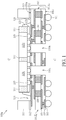
- Fig. 1 is a cross-sectional view of a semiconductor package structure 100a according to one embodiment of the disclosure.
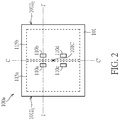
- Fig. 2 is a plan view of an arrangement of holes in a substrate 101 of the semiconductor package structure 100a shown in Fig. 1, and
- Fig. 1 is a cross-sectional view of the semiconductor package structure 100a along line I-I' of Fig. 2 .
- the semiconductor package structure 100a may include a wafer-level semiconductor package, for example, a flip-chip semiconductor package.
- the semiconductor package structure 100a may be mounted on a base (not shown).
- the semiconductor package structure 100a may be a system-on-chip (SOC) package structure.
- the base may include a printed circuit board (PCB) and may be formed of polypropylene (PP).
- the base may include a package substrate.
- the semiconductor package structure 100a may be mounted on the base by a bonding process.
- the semiconductor package structure 100a may include bump structures 111.
- the bump structures 111 may be conductive ball structures (such as ball grid array (BGA)), conductive pillar structures, or conductive paste structures that are mounted on and electrically coupled to the base by the bonding process.
- BGA ball grid array
- the semiconductor package structure 100a may include a substrate 101.
- the substrate 101 has a wiring structure therein.
- the wiring structure in the substrate 101 may be a fan-out structure, and may include one or more conductive pads 103, conductive vias 105, conductive layers 107 and conductive pillars 109.
- the wiring structure in the substrate 101 may be disposed in one or more inter-metal dielectric (IMD) layers.
- the IMD layers may be formed of organic materials, which include a polymer base material, non-organic materials, which include silicon nitride (SiN x ), silicon oxide (SiO x ), grapheme, or the like.
- the IMD layers are made of a polymer base material. It should be noted that the number and configuration of the IMD layers, the conductive pads 103, the conductive vias 105, the conductive layers 107 and the conductive pillars 109 shown in the figures and only some examples and are not limitations to the present invention.
- the semiconductor package structure 100a further comprises a first semiconductor die 115a and a second semiconductor die 115b bonded onto the substrate 101 through a plurality of conductive structures 119.
- the substrate 101 has a first surface 101a and a second surface 101b opposite thereto, the first surface 101a is facing the first semiconductor die 115a and the second semiconductor die 115b, and the second surface 101b is facing the above-mentioned base.
- the conductive structures 119 are disposed over the first surface 101a and below the first semiconductor die 115a and the second semiconductor die 115b, and the bump structures 111 are disposed on the second surface 101b of the substrate 101.
- the first semiconductor die 115a and the second semiconductor die 115b are electrically coupled to the bump structures 111 through the conductive structures 119 and the wiring structure in the substrate 101.
- the conductive structures 119 may be controlled collapse chip connection (C4) structures. It should be noted that the number of semiconductor dies integrated in the semiconductor package structure 100a is not limited to that disclosed in the embodiment.
- the first semiconductor die 115a and the second semiconductor die 115b are active devices.
- the first semiconductor die 115a and the second semiconductor die 115b may be logic dies including a central processing unit (CPU), a graphics processing unit (GPU), a dynamic random access memory (DRAM) controller, or any combinations thereof.
- one or more passive devices are also bonded onto the substrate 101.
- the first semiconductor die 115a and the second semiconductor dies 115b are arranged side-by-side.
- the first semiconductor die 115a and the second semiconductor dies 115b are separated by a molding material 117.
- the molding material 117 surrounds the first semiconductor die 115a and the second semiconductor die 115b, and adjoins the sidewalls of the first semiconductor die 115a and the second semiconductor die 115b.
- the molding material 117 includes a nonconductive material such as an epoxy, a resin, a moldable polymer, or another suitable molding material.
- the molding material 117 is applied as a substantial liquid, and then is cured through a chemical reaction.
- the molding material 117 is an ultraviolet (UV) or thermally cured polymer applied as a gel or malleable solid, and then is cured through a UV or thermal curing process.
- the molding material 117 may be cured with a mold (not shown).
- the surfaces of the first semiconductor die 115a and the second semiconductor dies 115b facing away from the first surface 101a of the substrate 101 are exposed by the molding material 117, such that a heat dissipating device (not shown) can directly attached to the surfaces of the first semiconductor die 115a and the second semiconductor dies 115b.
- a heat dissipating device (not shown) can directly attached to the surfaces of the first semiconductor die 115a and the second semiconductor dies 115b.
- the heat-dissipation efficiency of the semiconductor package structure 100a can be improved, particularly for a large semiconductor package structure, such as 50 mm ⁇ 50 mm, which is preferred for high power applications.
- the semiconductor package structure 100a may further include a polymer material 121 disposed under the molding material 117, the first semiconductor die 115a and the second semiconductor die 115b, and between the conductive structures 119.
- the semiconductor package structure 100a may further include an underfill layer 123 interposed between the first surface 101a of the substrate 101 and the polymer material 121.
- the first semiconductor die 115a, the second semiconductor dies 115b and the molding material 117 are surrounded by the underfill layer 123.
- the polymer material 121 and the underfill layer 123 are disposed to compensate for differing coefficients of thermal expansion (CTEs) between the substrate 101, the conductive structures 119, the first semiconductor die 115a and the second semiconductor dies 115b.
- CTEs coefficients of thermal expansion
- the semiconductor package structure 100a includes a frame 113 attached to the first surface 101a of the substrate 101 through an adhesive layer 112.
- the first semiconductor die 115a and the second semiconductor die 115b are surrounded by the frame 113 and the adhesive layer 112.
- the frame 113 and the adhesive layer 112 are separated from the underfill layer 121 by a gap 124.
- the substrate 101 has a first edge 101E 1 and a second edge 101E 2 opposite thereto.
- the first edge 101 E 1 and the second edge 101E 2 may be coplanar with sidewalls of the frame 113 and the adhesive layer 112.
- the substrate 101 of the semiconductor package structure 100a includes a first hole 110a and a second hole 110b formed on the second surface 101b.
- at least one of the first hole 110a and the second hole 110b penetrates through the substrate 101 from the first surface 101a to the second surface 101b.
- the first hole 110a and the second hole 110b shown in Fig. 1 penetrate through the substrate 101, in particular, both the first hole 110a and the second hole 110b do not penetrate through the substrate 101 from the first surface 101a to the second surface 101b.
- the first hole 110a is covered by the first semiconductor die 115a
- the second hole 110b is covered by the second semiconductor die 115b.
- the first hole 110a is located within the projection of the first semiconductor die 115a on the substrate 101
- the second hole 110b is located within the projection of the second semiconductor die 115b on the substrate 101.
- the first semiconductor die 115a and the second semiconductor die 115b have a center line C-C' between them.
- the first hole 110a is disposed closer to the center line C-C' than the first edge 101E 1 of the substrate 101
- the second hole 110b is disposed closer to the center line C-C' than the second edge 101E 2 of the substrate 101.
- the first hole 110a and the second hole 110b may be formed by a laser drilling process or another suitable process. It should be noted that the first hole 110a and the second hole 110b may be formed by the same forming process for the conductive pillars 109 in the wiring structure of the substrate 101. Moreover, the first semiconductor die 115a and the second semiconductor die 115b are bonded to the substrate 101 after forming the holes in the substrate 101. Therefore, the damage of the first semiconductor die 115a and the second semiconductor die 115b can be prevented.
- Fig. 2 which is a plan view of an arrangement of holes in a substrate 101 of the semiconductor package structure 100a shown in Fig. 1, and Fig. 1 is a cross-sectional view of the semiconductor package structure 100a along line I-I' of Fig. 2 .
- Fig. 2 is the plan view from the bottom of the semiconductor package structure 100a.
- Fig. 2 is the plan view from the second surface 101b of the substrate 101, which the bump structures 111 are disposed on.
- the bump structures 111 are omitted for brevity.
- the substrate 101 may include more than two holes.
- the substrate 101 may further include a third hole 110c and the fourth hole 110d formed on the second surface 101b.
- the third hole 110c is covered by the first semiconductor die 115a
- the fourth hole 110d is covered by the second semiconductor die 115b.
- the substrate 101 has a center 101C, and the first hole 101a, the second hole 101b, the third hole 110c, and the fourth hole 110d are disposed closer to the center 101C than the first edge 101E 1 and the second edge 101E 2 of the substrate 101.
- the holes formed in the substrate 101 are designed to release the stress in the substrate 101, especially the stress concentrated in the region below the interface between two semiconductor dies (i.e. the first semiconductor die 115a and the second semiconductor die 115b). Since the semiconductor package structure 100a may be highly stressed due to the different coefficients of thermal expansion (CTEs) of the substrate 101 and the semiconductor dies, the holes formed in the substrate 101 can solve the warping or cracking problems caused by mismatched CTEs. As a result, the electrical connection within the semiconductor package structure 100a may not be damaged, and the reliability of the semiconductor package structure 100a may be increased.
- CTEs coefficients of thermal expansion
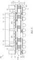
- Fig. 3 is a cross-sectional view of a semiconductor package structure 100b according to another embodiment of the disclosure. Descriptions of elements of the embodiments hereinafter that are the same as or similar to those previously described with reference to Fig. 1 are omitted for brevity.
- the semiconductor package structure 100b includes a stress buffer layer 125 filled in the first hole 110a and the second hole 110b.
- the stress buffer layer 125 is made of a polymer material, such as a silicone resin or rubber.
- the stress buffer layer 125 is made of an organic resin, such as Ajinomoto Build-up Film (ABF).
- the stress buffer layer 125 may be formed by a spin coating process.
- a material of the stress buffer layer 125 may be dispensed in the first hole 110a and the second hole 110b, and an excess portion of the material of the stress buffer layer 125 may be removed.
- the stress buffer layer 125 may be formed before bonding the first semiconductor die 115a and the second semiconductor die 115b to the substrate 101.
- the stress buffer layer 125 may filled up the first hole 110a and the second hole 110b, and the surfaces of the stress buffer layer 125 are level with the second surface 101b of the substrate 101.
- the surfaces of the stress buffer layer 125 may not be level with the second surface 101b of the substrate 101 according to the actual manufacturing processes.
- Filling the first hole 110a and the second hole 110b with the stress buffer layer 125 may offer advantages like preventing the impurities and dusts from dropping into the first hole 110a and the second hole 110b during the handling process of the substrate 101.
- the warping or cracking problems caused by mismatched coefficients of thermal expansion in the semiconductor package structure 100b can be solved by the holes (including the first hole 110a and the second hole 110b) and the stress buffer layer 125 formed in the substrate 101. Accordingly, the electrical connection within the semiconductor package structure 100b may not be damaged, and the lifespan of the semiconductor package structure 100b may be increased.
- Fig. 4 is a schematic plan view of a semiconductor package structure 100c according to still another embodiment of the disclosure.
- Fig. 5 is a schematic, cross-sectional diagram taken along line II-II' in Fig. 4 .
- Like layers, regions or elements are designated by like numeral numbers.
- the semiconductor package structure 100c comprises a first semiconductor die 115a and a second semiconductor die 115b mounted on the substrate 101 through a plurality of conductive structures 119.
- the substrate 101 has a first surface 101a and a second surface 101b opposite thereto, the first surface 101a is facing the first semiconductor die 115a and the second semiconductor die 115b, and the second surface 101b is facing the above-mentioned base such as a PCB or a system board.
- the conductive structures 119 are disposed over the first surface 101a and below the first semiconductor die 115a and the second semiconductor die 115b, and the bump structures 111 are disposed on the second surface 101b of the substrate 101.
- the bump structures 111 may be a ball grid array (BGA) or a land grid array (LGA).
- a heat sink 130 may be mounted on the first semiconductor die 115a and the second semiconductor die 115b for heat dissipation.
- the semiconductor package structure 100c comprises a continuous, annular frame 113 mounted on the first surface 101a of the substrate 101.
- the frame 113 may have a substantially rectangular shape when viewed from the above.
- the frame 113 may be made of metal or metal alloys.
- the frame 113 may be made of copper, but is not limited thereto.
- the frame 113 may be attached to the first surface 101a of the substrate 101 through the adhesive layer 112.
- the frame 113 has four bevel angles at its four corners, instead of the four right-angle corners as depicted in FIG. 2 . Portions of the frame within the retracted regions 113a, which are indicated by dashed lines, may be truncated from the frame 113 by any suitable cutting means to form the bevel angles at the four corners of the frame 113.
- a securing means such as a socket (not shown) may be provided on the frame 113 to secure the substrate 101 to the aforesaid base such as a PCB or a system board.
- the socket may exert undesired mechanical stress onto the frame 113 and the substrate 101 and may cause damage or defects such as fractures in the substrate 101.
- a frame 113 with a wider width w is desired.
- the frame with a wider width makes the warpage problem worse.
- the present disclosure solves the warpage problem by truncating the corners of the frame 113, thereby eliminating or reducing the warpage when a frame with wider width is used.
- each of the retracted regions 113a may be of a right-triangle shape, but is not limited thereto.
- each of the retracted regions 113a may be of a rectangular shape, as the semiconductor package structure 100d depicted in FIG. 6 .
- the shapes of the truncated edge at the four corners of the frame 113 in FIG. 4 and FIG. 6 are for illustration purposes only.
- the shapes of the truncated edge may comprise arc shapes, curved shapes or irregular shapes.
- the cut shape at the four corners of the frame 113 may depend upon design requirements in order to obtain improvement on package warpage, stress distribution and cost.
- the adhesive layer 112 within the retracted regions 113a may be exposed after the truncated frame 113 is mounted on the first surface 101a of the substrate 101.
- the frame 113 has a width w, which may range between 1 mm and 18 mm, for example, 12 mm.
- the width w of the frame 113 may be greater than or equal to 1 mm.
- the area of each of the right-triangle shaped retracted regions 113a is presented by d 2 /2, wherein d is the length of the sides or legs of the right-triangle shaped retracted regions 113a.
- the length d is greater than or equal to w/2.
- Fig. 7 is a schematic plan view of a semiconductor package structure 100e according to yet another embodiment of the disclosure.
- the difference between the semiconductor package structure 100e in Fig. 7 and the semiconductor package structure 100c in Fig. 4 is that the frame 113 of the semiconductor package structure 100e in Fig. 7 comprises an extension portion 113b that inwardly extends at the inner corners of the frame 113. Therefore, the inner corners of the frame 113 comprise no right angle.
- the removed right-triangle shaped retracted regions 113a at the outer corners of the frame 113 may be compensated by adding the extension portions 113b at the inner corners of the frame 113, which are indicated by dashed lines. It is beneficial to do so because the overall surface of the frame 113 for mounting the socket may be maintained and the stress exerted by the socket or the securing means of the socket may be more evenly distributed across the frame 113.
Landscapes
- Structures Or Materials For Encapsulating Or Coating Semiconductor Devices Or Solid State Devices (AREA)
Abstract
Description
- This application is a continuation-in-part of
U.S. application Ser. No. 15/906,098 filed February 27, 2018 U.S. provisional application No. 62/470,915 filed on March 14, 2017 U.S. provisional application No. 62/729,541 filed on September 11, 2018 - The present invention relates to a semiconductor package structure, and more particularly, to a semiconductor package structure with an annular frame disposed on a top surface of a package substrate therein.
- A semiconductor package cannot only provide a semiconductor die with protection from environmental contaminants, but it can also provide an electrical connection between the semiconductor die packaged therein and a substrate, such as a printed circuit board (PCB). For instance, a semiconductor die may be enclosed in an encapsulating material, and traces are electrically connected to the semiconductor die and the substrate.
- However, a problem with such a semiconductor package is that it is subject to different temperatures during the packaging process. The semiconductor package may be highly stressed due to the different coefficients of thermal expansion (CTEs) of the various substrate and semiconductor die materials. As a result, the semiconductor package may exhibit warping or cracking so that the electrical connection between the semiconductor die and the substrate may be damaged, and the reliability of the semiconductor package may be decreased.
- This problem is exacerbated in the case of a relatively large package, for example a package of 50 mm × 50 mm or larger. Therefore, a novel semiconductor package structure is desirable.
- Semiconductor package structures according to the invention are defined in the independent claims. The dependent claims define preferred embodiments thereof. It is one object of the present disclosure to provide an improved semiconductor package structure with an annular frame in order to solve the above-mentioned prior art shortcomings or problems.
- According to one aspect of the present disclosure, a semiconductor package structure includes a substrate having a first surface and second surface opposite thereto, a first semiconductor die disposed on the first surface of the substrate, a second semiconductor die disposed on the first surface, a molding material surrounding the first semiconductor die and the second semiconductor die, and an annular frame mounted on the first surface of the substrate. The first semiconductor die and the second semiconductor die are arranged in a side-by-side manner. The first semiconductor die is separated from the second semiconductor die by the molding material. The substrate comprises a wiring structure. The first semiconductor die and the second semiconductor die are electrically coupled to the wiring structure. The annular frame surrounds the first semiconductor die and the second semiconductor die. The annular frame comprises a retracted region at an outer corner of the annular frame.
- Preferably, the annular frame has a substantially rectangular shape when viewed from above.
- Preferably, a portion of the frame within the retracted region is truncated from the annular frame, thereby form a bevel angle at the outer corner of the annular frame.
- Preferably, the semiconductor package structure further comprises bump structures disposed on the second surface of the substrate.
- Preferably, the bump structures are a land grid array (LGA).
- Preferably, a securing means is provided on the annular frame to secure the substrate to a base.
- Preferably, the base comprises a PCB or a system board.
- Preferably, the securing means comprises a socket.
- Preferably, the semiconductor package structure further comprises an adhesive layer between the annular frame and the first surface of the substrate.
- Preferably, the adhesive layer is not covered by the annular frame within the retracted region.
- Preferably, the annular frame has a width w, and wherein w ranges between 3 mm and 18 mm.
- Preferably, the retracted region has a right-triangle shape.
- Preferably, an area of the right-triangle shaped retracted regions is presented by d2/2, wherein d is the length of the sides of legs of the right-triangle shaped retracted regions, and wherein d is greater than or equal to w/2.
- Preferably, the semiconductor package structure according to claim 1 further comprising an extension portion that inwardly extends at an inner corner of the annular frame.
- These and other objectives of the present invention will no doubt become obvious to those of ordinary skill in the art after reading the following detailed description of the preferred embodiment that is illustrated in the various figures and drawings.
- The present invention can be more fully understood by reading the subsequent detailed description and examples with references made to the accompanying drawings, wherein:
-
Fig. 1 is a cross-sectional view of a semiconductor package structure according to one embodiment of the disclosure; -
Fig. 2 is a plan view of an arrangement of holes in a substrate of the semiconductor package structure shown inFig. 1, and Fig. 1 is a cross-sectional view of the semiconductor package structure along line I-I' ofFig. 2 ; -
Fig. 3 is a cross-sectional view of a semiconductor package structure according to another embodiment of the disclosure; -
Fig. 4 is a schematic plan view of a semiconductor package structure according to still another embodiment of the disclosure; -
Fig. 5 is a schematic, cross-sectional diagram taken along line II-II' inFig. 4 ; -
Fig. 6 is a schematic plan view of a semiconductor package structure according to still another embodiment of the disclosure; and -
Fig. 7 is a schematic plan view of a semiconductor package structure according to yet another embodiment of the disclosure. - The following description is of the best-contemplated mode of carrying out the invention. This description is made for the purpose of illustrating the general principles of the invention and should not be taken in a limiting sense. The scope of the invention is determined by reference to the appended claims.
- The present invention will be described with respect to particular embodiments and with reference to certain drawings, but the invention is not limited thereto and is only limited by the claims. The drawings described are only schematic and are non-limiting. In the drawings, the size of some of the elements may be exaggerated for illustrative purposes and not drawn to scale. The dimensions and the relative dimensions do not correspond to actual dimensions in the practice of the invention.
-
Fig. 1 is a cross-sectional view of asemiconductor package structure 100a according to one embodiment of the disclosure.Fig. 2 is a plan view of an arrangement of holes in asubstrate 101 of thesemiconductor package structure 100a shown inFig. 1, and Fig. 1 is a cross-sectional view of thesemiconductor package structure 100a along line I-I' ofFig. 2 . - Additional features can be added to the
semiconductor package structure 100a. Some of the features described below can be replaced or eliminated for different embodiments. To simplify the diagram, only a portion of thesemiconductor package structure 100a is depicted inFigs. 1 and2 . Preferably, thesemiconductor package structure 100a may include a wafer-level semiconductor package, for example, a flip-chip semiconductor package. - Referring to
Fig. 1 , thesemiconductor package structure 100a may be mounted on a base (not shown). Preferably, thesemiconductor package structure 100a may be a system-on-chip (SOC) package structure. Moreover, the base may include a printed circuit board (PCB) and may be formed of polypropylene (PP). Preferably, the base may include a package substrate. Thesemiconductor package structure 100a may be mounted on the base by a bonding process. For example, thesemiconductor package structure 100a may includebump structures 111. Preferably, thebump structures 111 may be conductive ball structures (such as ball grid array (BGA)), conductive pillar structures, or conductive paste structures that are mounted on and electrically coupled to the base by the bonding process. - Preferably, the
semiconductor package structure 100a may include asubstrate 101. Thesubstrate 101 has a wiring structure therein. Preferably, the wiring structure in thesubstrate 101 may be a fan-out structure, and may include one or moreconductive pads 103,conductive vias 105,conductive layers 107 andconductive pillars 109. In such cases, the wiring structure in thesubstrate 101 may be disposed in one or more inter-metal dielectric (IMD) layers. Preferably, the IMD layers may be formed of organic materials, which include a polymer base material, non-organic materials, which include silicon nitride (SiNx), silicon oxide (SiOx), grapheme, or the like. For example, the IMD layers are made of a polymer base material. It should be noted that the number and configuration of the IMD layers, theconductive pads 103, theconductive vias 105, theconductive layers 107 and theconductive pillars 109 shown in the figures and only some examples and are not limitations to the present invention. - Moreover, the
semiconductor package structure 100a further comprises afirst semiconductor die 115a and asecond semiconductor die 115b bonded onto thesubstrate 101 through a plurality ofconductive structures 119. Thesubstrate 101 has afirst surface 101a and asecond surface 101b opposite thereto, thefirst surface 101a is facing thefirst semiconductor die 115a and thesecond semiconductor die 115b, and thesecond surface 101b is facing the above-mentioned base. Theconductive structures 119 are disposed over thefirst surface 101a and below thefirst semiconductor die 115a and thesecond semiconductor die 115b, and thebump structures 111 are disposed on thesecond surface 101b of thesubstrate 101. - Preferably, the
first semiconductor die 115a and thesecond semiconductor die 115b are electrically coupled to thebump structures 111 through theconductive structures 119 and the wiring structure in thesubstrate 101. In addition, theconductive structures 119 may be controlled collapse chip connection (C4) structures. It should be noted that the number of semiconductor dies integrated in thesemiconductor package structure 100a is not limited to that disclosed in the embodiment. - Preferably, the
first semiconductor die 115a and thesecond semiconductor die 115b are active devices. For example, thefirst semiconductor die 115a and thesecond semiconductor die 115b may be logic dies including a central processing unit (CPU), a graphics processing unit (GPU), a dynamic random access memory (DRAM) controller, or any combinations thereof. Preferably, one or more passive devices are also bonded onto thesubstrate 101. - The
first semiconductor die 115a and the second semiconductor dies 115b are arranged side-by-side. Preferably, thefirst semiconductor die 115a and the second semiconductor dies 115b are separated by amolding material 117. Themolding material 117 surrounds thefirst semiconductor die 115a and thesecond semiconductor die 115b, and adjoins the sidewalls of thefirst semiconductor die 115a and thesecond semiconductor die 115b. Preferably, themolding material 117 includes a nonconductive material such as an epoxy, a resin, a moldable polymer, or another suitable molding material. Preferably, themolding material 117 is applied as a substantial liquid, and then is cured through a chemical reaction. Preferably, themolding material 117 is an ultraviolet (UV) or thermally cured polymer applied as a gel or malleable solid, and then is cured through a UV or thermal curing process. Themolding material 117 may be cured with a mold (not shown). - Preferably, the surfaces of the
first semiconductor die 115a and the second semiconductor dies 115b facing away from thefirst surface 101a of thesubstrate 101 are exposed by themolding material 117, such that a heat dissipating device (not shown) can directly attached to the surfaces of thefirst semiconductor die 115a and the second semiconductor dies 115b. As a result, the heat-dissipation efficiency of thesemiconductor package structure 100a can be improved, particularly for a large semiconductor package structure, such as 50 mm × 50 mm, which is preferred for high power applications. - The
semiconductor package structure 100a may further include apolymer material 121 disposed under themolding material 117, thefirst semiconductor die 115a and thesecond semiconductor die 115b, and between theconductive structures 119. Thesemiconductor package structure 100a may further include anunderfill layer 123 interposed between thefirst surface 101a of thesubstrate 101 and thepolymer material 121. Preferably, thefirst semiconductor die 115a, the second semiconductor dies 115b and themolding material 117 are surrounded by theunderfill layer 123. Thepolymer material 121 and theunderfill layer 123 are disposed to compensate for differing coefficients of thermal expansion (CTEs) between thesubstrate 101, theconductive structures 119, thefirst semiconductor die 115a and the second semiconductor dies 115b. - In addition, the
semiconductor package structure 100a includes aframe 113 attached to thefirst surface 101a of thesubstrate 101 through anadhesive layer 112. Thefirst semiconductor die 115a and thesecond semiconductor die 115b are surrounded by theframe 113 and theadhesive layer 112. Preferably, theframe 113 and theadhesive layer 112 are separated from theunderfill layer 121 by agap 124. Thesubstrate 101 has afirst edge 101E1 and asecond edge 101E2 opposite thereto. Preferably, thefirst edge 101 E1 and thesecond edge 101E2 may be coplanar with sidewalls of theframe 113 and theadhesive layer 112. - Still referring to
Fig. 1 , thesubstrate 101 of thesemiconductor package structure 100a includes afirst hole 110a and asecond hole 110b formed on thesecond surface 101b. Preferably, at least one of thefirst hole 110a and thesecond hole 110b penetrates through thesubstrate 101 from thefirst surface 101a to thesecond surface 101b. Although thefirst hole 110a and thesecond hole 110b shown inFig. 1 penetrate through thesubstrate 101, in particular, both thefirst hole 110a and thesecond hole 110b do not penetrate through thesubstrate 101 from thefirst surface 101a to thesecond surface 101b. Preferably, thefirst hole 110a is covered by thefirst semiconductor die 115a, and thesecond hole 110b is covered by thesecond semiconductor die 115b. In other words, thefirst hole 110a is located within the projection of thefirst semiconductor die 115a on thesubstrate 101, and thesecond hole 110b is located within the projection of thesecond semiconductor die 115b on thesubstrate 101. - Specifically, the
first semiconductor die 115a and thesecond semiconductor die 115b have a center line C-C' between them. Thefirst hole 110a is disposed closer to the center line C-C' than thefirst edge 101E1 of thesubstrate 101, and thesecond hole 110b is disposed closer to the center line C-C' than thesecond edge 101E2 of thesubstrate 101. Although there are only two holes in thesubstrate 101 shown inFig. 1 , it should be noted that there is no limitation on the number of the holes formed in thesubstrate 101. - Preferably, the
first hole 110a and thesecond hole 110b may be formed by a laser drilling process or another suitable process. It should be noted that thefirst hole 110a and thesecond hole 110b may be formed by the same forming process for theconductive pillars 109 in the wiring structure of thesubstrate 101. Moreover, thefirst semiconductor die 115a and thesecond semiconductor die 115b are bonded to thesubstrate 101 after forming the holes in thesubstrate 101. Therefore, the damage of thefirst semiconductor die 115a and thesecond semiconductor die 115b can be prevented. - Referring to
Fig. 2 , which is a plan view of an arrangement of holes in asubstrate 101 of thesemiconductor package structure 100a shown inFig. 1, and Fig. 1 is a cross-sectional view of thesemiconductor package structure 100a along line I-I' ofFig. 2 . It should be noted thatFig. 2 is the plan view from the bottom of thesemiconductor package structure 100a. In other words,Fig. 2 is the plan view from thesecond surface 101b of thesubstrate 101, which thebump structures 111 are disposed on. In particular, thebump structures 111 are omitted for brevity. - As shown in
Fig. 2 , thesubstrate 101 may include more than two holes. In particular, thesubstrate 101 may further include athird hole 110c and thefourth hole 110d formed on thesecond surface 101b. Thethird hole 110c is covered by thefirst semiconductor die 115a, and thefourth hole 110d is covered by thesecond semiconductor die 115b. It should be noted that thesubstrate 101 has acenter 101C, and thefirst hole 101a, thesecond hole 101b, thethird hole 110c, and thefourth hole 110d are disposed closer to thecenter 101C than thefirst edge 101E1 and thesecond edge 101E2 of thesubstrate 101. - The holes formed in the
substrate 101, for example, thefirst hole 110a, thesecond hole 110b, thethird hole 110c and thefourth hole 110d, are designed to release the stress in thesubstrate 101, especially the stress concentrated in the region below the interface between two semiconductor dies (i.e. thefirst semiconductor die 115a and thesecond semiconductor die 115b). Since thesemiconductor package structure 100a may be highly stressed due to the different coefficients of thermal expansion (CTEs) of thesubstrate 101 and the semiconductor dies, the holes formed in thesubstrate 101 can solve the warping or cracking problems caused by mismatched CTEs. As a result, the electrical connection within thesemiconductor package structure 100a may not be damaged, and the reliability of thesemiconductor package structure 100a may be increased. -
Fig. 3 is a cross-sectional view of asemiconductor package structure 100b according to another embodiment of the disclosure. Descriptions of elements of the embodiments hereinafter that are the same as or similar to those previously described with reference toFig. 1 are omitted for brevity. - As shown in
Fig. 3 , thesemiconductor package structure 100b includes astress buffer layer 125 filled in thefirst hole 110a and thesecond hole 110b. Thestress buffer layer 125 is made of a polymer material, such as a silicone resin or rubber. Preferably, thestress buffer layer 125 is made of an organic resin, such as Ajinomoto Build-up Film (ABF). - Moreover, the
stress buffer layer 125 may be formed by a spin coating process. In particular, a material of thestress buffer layer 125 may be dispensed in thefirst hole 110a and thesecond hole 110b, and an excess portion of the material of thestress buffer layer 125 may be removed. Preferably, thestress buffer layer 125 may be formed before bonding thefirst semiconductor die 115a and thesecond semiconductor die 115b to thesubstrate 101. - Preferably, the
stress buffer layer 125 may filled up thefirst hole 110a and thesecond hole 110b, and the surfaces of thestress buffer layer 125 are level with thesecond surface 101b of thesubstrate 101. In particular, the surfaces of thestress buffer layer 125 may not be level with thesecond surface 101b of thesubstrate 101 according to the actual manufacturing processes. - Filling the
first hole 110a and thesecond hole 110b with thestress buffer layer 125 may offer advantages like preventing the impurities and dusts from dropping into thefirst hole 110a and thesecond hole 110b during the handling process of thesubstrate 101. In addition, the warping or cracking problems caused by mismatched coefficients of thermal expansion in thesemiconductor package structure 100b can be solved by the holes (including thefirst hole 110a and thesecond hole 110b) and thestress buffer layer 125 formed in thesubstrate 101. Accordingly, the electrical connection within thesemiconductor package structure 100b may not be damaged, and the lifespan of thesemiconductor package structure 100b may be increased. - Please refer to
Fig. 4 andFig. 5 .Fig. 4 is a schematic plan view of asemiconductor package structure 100c according to still another embodiment of the disclosure.Fig. 5 is a schematic, cross-sectional diagram taken along line II-II' inFig. 4 . Like layers, regions or elements are designated by like numeral numbers. - As shown in
FIG. 4 andFIG. 5 , likewise, thesemiconductor package structure 100c comprises afirst semiconductor die 115a and asecond semiconductor die 115b mounted on thesubstrate 101 through a plurality ofconductive structures 119. Thesubstrate 101 has afirst surface 101a and asecond surface 101b opposite thereto, thefirst surface 101a is facing thefirst semiconductor die 115a and thesecond semiconductor die 115b, and thesecond surface 101b is facing the above-mentioned base such as a PCB or a system board. Theconductive structures 119 are disposed over thefirst surface 101a and below thefirst semiconductor die 115a and thesecond semiconductor die 115b, and thebump structures 111 are disposed on thesecond surface 101b of thesubstrate 101. Thebump structures 111 may be a ball grid array (BGA) or a land grid array (LGA). According to one embodiment, aheat sink 130 may be mounted on thefirst semiconductor die 115a and thesecond semiconductor die 115b for heat dissipation. - According to one embodiment, the
semiconductor package structure 100c comprises a continuous,annular frame 113 mounted on thefirst surface 101a of thesubstrate 101. According to one embodiment, theframe 113 may have a substantially rectangular shape when viewed from the above. According to one embodiment, theframe 113 may be made of metal or metal alloys. For example, theframe 113 may be made of copper, but is not limited thereto. Theframe 113 may be attached to thefirst surface 101a of thesubstrate 101 through theadhesive layer 112. According to the embodiment, theframe 113 has four bevel angles at its four corners, instead of the four right-angle corners as depicted inFIG. 2 . Portions of the frame within the retractedregions 113a, which are indicated by dashed lines, may be truncated from theframe 113 by any suitable cutting means to form the bevel angles at the four corners of theframe 113. - In a case that the
bump structures 111 are LGA arrangement, a securing means such as a socket (not shown) may be provided on theframe 113 to secure thesubstrate 101 to the aforesaid base such as a PCB or a system board. The socket may exert undesired mechanical stress onto theframe 113 and thesubstrate 101 and may cause damage or defects such as fractures in thesubstrate 101. To alleviate such stress caused by the socket, aframe 113 with a wider width w is desired. However, the frame with a wider width makes the warpage problem worse. The present disclosure solves the warpage problem by truncating the corners of theframe 113, thereby eliminating or reducing the warpage when a frame with wider width is used. - According to one embodiment, each of the retracted
regions 113a may be of a right-triangle shape, but is not limited thereto. Preferably, for example, each of the retractedregions 113a may be of a rectangular shape, as thesemiconductor package structure 100d depicted inFIG. 6 . It is understood that the shapes of the truncated edge at the four corners of theframe 113 inFIG. 4 andFIG. 6 are for illustration purposes only. Preferably, the shapes of the truncated edge may comprise arc shapes, curved shapes or irregular shapes. The cut shape at the four corners of theframe 113 may depend upon design requirements in order to obtain improvement on package warpage, stress distribution and cost. According to one embodiment, theadhesive layer 112 within the retractedregions 113a may be exposed after thetruncated frame 113 is mounted on thefirst surface 101a of thesubstrate 101. - Preferably, the
frame 113 has a width w, which may range between 1 mm and 18 mm, for example, 12 mm. Preferably, the width w of theframe 113 may be greater than or equal to 1 mm. In particular, the area of each of the right-triangle shaped retractedregions 113a is presented by d2/2, wherein d is the length of the sides or legs of the right-triangle shaped retractedregions 113a. Preferably, the length d is greater than or equal to w/2. By providing such right-triangle shaped retractedregions 113a in theframe 113 and/or theadhesive layer 112, the warpage control of thesemiconductor package structure 100c can be significantly improved. -
Fig. 7 is a schematic plan view of asemiconductor package structure 100e according to yet another embodiment of the disclosure. As shown inFig. 7 , the difference between thesemiconductor package structure 100e inFig. 7 and thesemiconductor package structure 100c inFig. 4 is that theframe 113 of thesemiconductor package structure 100e inFig. 7 comprises anextension portion 113b that inwardly extends at the inner corners of theframe 113. Therefore, the inner corners of theframe 113 comprise no right angle. By providing such configuration, the removed right-triangle shaped retractedregions 113a at the outer corners of theframe 113 may be compensated by adding theextension portions 113b at the inner corners of theframe 113, which are indicated by dashed lines. It is beneficial to do so because the overall surface of theframe 113 for mounting the socket may be maintained and the stress exerted by the socket or the securing means of the socket may be more evenly distributed across theframe 113. - Those skilled in the art will readily observe that numerous modifications and alterations of the device and method may be made while retaining the teachings of the invention. Accordingly, the above disclosure should be construed as limited only by the metes and bounds of the appended claims.
Claims (15)
- A semiconductor package structure (100a, 100d), comprising:a substrate (101) having a first surface (101a) and second surface (101b) opposite thereto, wherein the substrate comprises a wiring structure;a first semiconductor die (115a) disposed on the first surface of the substrate and electrically coupled to the wiring structure;a second semiconductor die (115b) disposed on the first surface and electrically coupled to the wiring structure, wherein the first semiconductor die and the second semiconductor die are arranged in a side-by-side manner;a molding material (117) surrounding the first semiconductor die and the second semiconductor die, wherein the first semiconductor die is separated from the second semiconductor die by the molding material; andan annular frame (113) mounted on the first surface of the substrate, wherein the annular frame surrounds the first semiconductor die (115a) and the second semiconductor die (115b), wherein the annular frame (113) comprises a retracted region at an outer corner of the annular frame.
- The semiconductor package structure (100a, 100d) according to claim 1, wherein the annular frame (113) has a substantially rectangular shape when viewed from above.
- The semiconductor package structure (100a, 100d) according to claim 1, wherein a portion of the frame within the retracted region is truncated from the annular frame (113), thereby form a bevel angle at the outer corner of the annular frame (113).
- The semiconductor package structure (100a, 100d) according to any one of the preceding claims further comprising bump structures (111) disposed on the second surface (101b) of the substrate.
- The semiconductor package structure (100a, 100d) according to claim 4, wherein the bump structures are a land grid array, in the following also referred to as LGA, wherein preferably a securing means is provided on the annular frame (113) to secure the substrate to a base.
- The semiconductor package structure (100a, 100d) according to claim 5, wherein the base comprises a PCB or a system board.
- The semiconductor package structure (100a, 100d) according to claim 5 or 6, wherein the securing means comprises a socket.
- The semiconductor package structure (100a, 100d) according to any one of the preceding claims further comprising an adhesive layer (112) between the annular frame (113) and the first surface (101a) of the substrate.
- The semiconductor package structure (100a, 100d) according to claim 8, wherein the adhesive layer is not covered by the annular frame (113) within the retracted region.
- The semiconductor package structure (100a, 100d) according to any one of the preceding claims, wherein the annular frame (113) has a width w, and wherein w is greater than or equal to 1 mm and/or ranges between 1 mm and 18 mm.
- The semiconductor package structure (100a, 100d) according to any one of the preceding claims, wherein the retracted region has a right-triangle shape.
- The semiconductor package structure (100a, 100d) according to claim 11, wherein an area of the right-triangle shaped retracted regions is presented by d2/2, wherein d is the length of the sides of legs of the right-triangle shaped retracted regions, and wherein d is greater than or equal to w/2.
- The semiconductor package structure (100a, 100d) according to any one of the preceding claims further comprising an extension portion that inwardly extends at an inner corner of the annular frame (113).
- A semiconductor package structure (100b), comprising:a substrate (101) having a first surface (101a) and second surface (101b) opposite thereto, wherein the substrate comprises a wiring structure;a first semiconductor die (115a) disposed on the first surface of the substrate and electrically coupled to the wiring structure;a second semiconductor die (115b) disposed on the first surface and electrically coupled to the wiring structure, wherein the first semiconductor die and the second semiconductor die are arranged in a side-by-side manner;a molding material (117) surrounding the first semiconductor die and the second semiconductor die, wherein the first semiconductor die is separated from the second semiconductor die by the molding material; andan annular frame (113) mounted on the first surface of the substrate, wherein the annular frame surrounds the first semiconductor die and the second semiconductor die, wherein the annular frame (113) comprises at least one bevel angles at an outer corner of the annular frame.
- A semiconductor package structure (100c), comprising:a substrate (101) having a first surface (101a) and second surface (101b) opposite thereto, wherein the substrate comprises a wiring structure;a first semiconductor die (115a) disposed on the first surface of the substrate and electrically coupled to the wiring structure;a second semiconductor die (115b) disposed on the first surface and electrically coupled to the wiring structure, wherein the first semiconductor die and the second semiconductor die are arranged in a side-by-side manner;a molding material (117) surrounding the first semiconductor die and the second semiconductor die, wherein the first semiconductor die is separated from the second semiconductor die by the molding material; andan annular frame (113) mounted on the first surface of the substrate, wherein the annular frame surrounds the first semiconductor die and the second semiconductor die, wherein the annular frame comprises a retracted region at an outer corner of the annular frame, and the annular frame has a substantially rectangular shape when viewed from above.
Applications Claiming Priority (2)
| Application Number | Priority Date | Filing Date | Title |
|---|---|---|---|
| US201862729541P | 2018-09-11 | 2018-09-11 | |
| US16/563,919 US11171113B2 (en) | 2017-03-14 | 2019-09-08 | Semiconductor package structure having an annular frame with truncated corners |
Publications (2)
| Publication Number | Publication Date |
|---|---|
| EP3624181A1 true EP3624181A1 (en) | 2020-03-18 |
| EP3624181B1 EP3624181B1 (en) | 2024-07-03 |
Family
ID=67953552
Family Applications (1)
| Application Number | Title | Priority Date | Filing Date |
|---|---|---|---|
| EP19196606.8A Active EP3624181B1 (en) | 2018-09-11 | 2019-09-11 | Semiconductor package structure having a frame with truncated corners |
Country Status (1)
| Country | Link |
|---|---|
| EP (1) | EP3624181B1 (en) |
Cited By (1)
| Publication number | Priority date | Publication date | Assignee | Title |
|---|---|---|---|---|
| CN114267645A (en) * | 2021-01-15 | 2022-04-01 | 台湾积体电路制造股份有限公司 | Packaging structure |
Citations (5)
| Publication number | Priority date | Publication date | Assignee | Title |
|---|---|---|---|---|
| US6020221A (en) * | 1996-12-12 | 2000-02-01 | Lsi Logic Corporation | Process for manufacturing a semiconductor device having a stiffener member |
| US20070069366A1 (en) * | 2005-09-29 | 2007-03-29 | Taiwan Semiconductor Manufacturing Co., Ltd. | Novel constraint stiffener design |
| US20090236730A1 (en) * | 2008-03-19 | 2009-09-24 | Roden Topacio | Die substrate with reinforcement structure |
| US20100276799A1 (en) * | 2009-05-04 | 2010-11-04 | Heng Stephen F | Semiconductor Chip Package with Stiffener Frame and Configured Lid |
| US20180138127A1 (en) * | 2015-04-17 | 2018-05-17 | Samsung Electro-Mechanics Co., Ltd. | Electronic component package and method of manufacturing the same |
Family Cites Families (1)
| Publication number | Priority date | Publication date | Assignee | Title |
|---|---|---|---|---|
| US9196805B2 (en) * | 2010-02-09 | 2015-11-24 | Nichia Corporation | Light emitting device and method for manufacturing light emitting device |
-
2019
- 2019-09-11 EP EP19196606.8A patent/EP3624181B1/en active Active
Patent Citations (5)
| Publication number | Priority date | Publication date | Assignee | Title |
|---|---|---|---|---|
| US6020221A (en) * | 1996-12-12 | 2000-02-01 | Lsi Logic Corporation | Process for manufacturing a semiconductor device having a stiffener member |
| US20070069366A1 (en) * | 2005-09-29 | 2007-03-29 | Taiwan Semiconductor Manufacturing Co., Ltd. | Novel constraint stiffener design |
| US20090236730A1 (en) * | 2008-03-19 | 2009-09-24 | Roden Topacio | Die substrate with reinforcement structure |
| US20100276799A1 (en) * | 2009-05-04 | 2010-11-04 | Heng Stephen F | Semiconductor Chip Package with Stiffener Frame and Configured Lid |
| US20180138127A1 (en) * | 2015-04-17 | 2018-05-17 | Samsung Electro-Mechanics Co., Ltd. | Electronic component package and method of manufacturing the same |
Cited By (1)
| Publication number | Priority date | Publication date | Assignee | Title |
|---|---|---|---|---|
| CN114267645A (en) * | 2021-01-15 | 2022-04-01 | 台湾积体电路制造股份有限公司 | Packaging structure |
Also Published As
| Publication number | Publication date |
|---|---|
| EP3624181B1 (en) | 2024-07-03 |
Similar Documents
| Publication | Publication Date | Title |
|---|---|---|
| US12525549B2 (en) | Semiconductor package structure | |
| US11862578B2 (en) | Semiconductor package structure | |
| US11942439B2 (en) | Semiconductor package structure | |
| EP3709344B1 (en) | Semiconductor package structure | |
| EP3754698B1 (en) | Semiconductor package structure | |
| US12142598B2 (en) | Semiconductor package structure having an annular frame with truncated corners | |
| TWI730891B (en) | A semiconductor package structure | |
| US12002742B2 (en) | Semiconductor package structure | |
| US20230307309A1 (en) | Semiconductor assemblies including vertically integrated circuits and methods of manufacturing the same | |
| EP3671831B1 (en) | Semiconductor package structure | |
| EP3624181B1 (en) | Semiconductor package structure having a frame with truncated corners | |
| US12424531B2 (en) | Semiconductor package structure |
Legal Events
| Date | Code | Title | Description |
|---|---|---|---|
| PUAI | Public reference made under article 153(3) epc to a published international application that has entered the european phase |
Free format text: ORIGINAL CODE: 0009012 |
|
| STAA | Information on the status of an ep patent application or granted ep patent |
Free format text: STATUS: THE APPLICATION HAS BEEN PUBLISHED |
|
| AK | Designated contracting states |
Kind code of ref document: A1 Designated state(s): AL AT BE BG CH CY CZ DE DK EE ES FI FR GB GR HR HU IE IS IT LI LT LU LV MC MK MT NL NO PL PT RO RS SE SI SK SM TR |
|
| AX | Request for extension of the european patent |
Extension state: BA ME |
|
| STAA | Information on the status of an ep patent application or granted ep patent |
Free format text: STATUS: REQUEST FOR EXAMINATION WAS MADE |
|
| 17P | Request for examination filed |
Effective date: 20200908 |
|
| RBV | Designated contracting states (corrected) |
Designated state(s): AL AT BE BG CH CY CZ DE DK EE ES FI FR GB GR HR HU IE IS IT LI LT LU LV MC MK MT NL NO PL PT RO RS SE SI SK SM TR |
|
| STAA | Information on the status of an ep patent application or granted ep patent |
Free format text: STATUS: EXAMINATION IS IN PROGRESS |
|
| 17Q | First examination report despatched |
Effective date: 20221117 |
|
| P01 | Opt-out of the competence of the unified patent court (upc) registered |
Effective date: 20230607 |
|
| GRAP | Despatch of communication of intention to grant a patent |
Free format text: ORIGINAL CODE: EPIDOSNIGR1 |
|
| STAA | Information on the status of an ep patent application or granted ep patent |
Free format text: STATUS: GRANT OF PATENT IS INTENDED |
|
| RIC1 | Information provided on ipc code assigned before grant |
Ipc: H01L 25/065 20060101ALI20240109BHEP Ipc: H01L 23/498 20060101ALI20240109BHEP Ipc: H01L 23/31 20060101ALI20240109BHEP Ipc: H01L 23/16 20060101ALI20240109BHEP Ipc: H01L 23/10 20060101AFI20240109BHEP |
|
| INTG | Intention to grant announced |
Effective date: 20240126 |
|
| GRAS | Grant fee paid |
Free format text: ORIGINAL CODE: EPIDOSNIGR3 |
|
| GRAA | (expected) grant |
Free format text: ORIGINAL CODE: 0009210 |
|
| STAA | Information on the status of an ep patent application or granted ep patent |
Free format text: STATUS: THE PATENT HAS BEEN GRANTED |
|
| AK | Designated contracting states |
Kind code of ref document: B1 Designated state(s): AL AT BE BG CH CY CZ DE DK EE ES FI FR GB GR HR HU IE IS IT LI LT LU LV MC MK MT NL NO PL PT RO RS SE SI SK SM TR |
|
| RAP3 | Party data changed (applicant data changed or rights of an application transferred) |
Owner name: MEDIATEK INC. |
|
| REG | Reference to a national code |
Ref country code: CH Ref legal event code: EP |
|
| REG | Reference to a national code |
Ref country code: DE Ref legal event code: R096 Ref document number: 602019054479 Country of ref document: DE |
|
| REG | Reference to a national code |
Ref country code: LT Ref legal event code: MG9D |
|
| REG | Reference to a national code |
Ref country code: NL Ref legal event code: MP Effective date: 20240703 |
|
| PG25 | Lapsed in a contracting state [announced via postgrant information from national office to epo] |
Ref country code: PT Free format text: LAPSE BECAUSE OF FAILURE TO SUBMIT A TRANSLATION OF THE DESCRIPTION OR TO PAY THE FEE WITHIN THE PRESCRIBED TIME-LIMIT Effective date: 20241104 |
|
| REG | Reference to a national code |
Ref country code: AT Ref legal event code: MK05 Ref document number: 1700742 Country of ref document: AT Kind code of ref document: T Effective date: 20240703 |
|
| PG25 | Lapsed in a contracting state [announced via postgrant information from national office to epo] |
Ref country code: NL Free format text: LAPSE BECAUSE OF FAILURE TO SUBMIT A TRANSLATION OF THE DESCRIPTION OR TO PAY THE FEE WITHIN THE PRESCRIBED TIME-LIMIT Effective date: 20240703 |
|
| PG25 | Lapsed in a contracting state [announced via postgrant information from national office to epo] |
Ref country code: PT Free format text: LAPSE BECAUSE OF FAILURE TO SUBMIT A TRANSLATION OF THE DESCRIPTION OR TO PAY THE FEE WITHIN THE PRESCRIBED TIME-LIMIT Effective date: 20241104 Ref country code: NL Free format text: LAPSE BECAUSE OF FAILURE TO SUBMIT A TRANSLATION OF THE DESCRIPTION OR TO PAY THE FEE WITHIN THE PRESCRIBED TIME-LIMIT Effective date: 20240703 |
|
| PG25 | Lapsed in a contracting state [announced via postgrant information from national office to epo] |
Ref country code: NO Free format text: LAPSE BECAUSE OF FAILURE TO SUBMIT A TRANSLATION OF THE DESCRIPTION OR TO PAY THE FEE WITHIN THE PRESCRIBED TIME-LIMIT Effective date: 20241003 |
|
| PG25 | Lapsed in a contracting state [announced via postgrant information from national office to epo] |
Ref country code: GR Free format text: LAPSE BECAUSE OF FAILURE TO SUBMIT A TRANSLATION OF THE DESCRIPTION OR TO PAY THE FEE WITHIN THE PRESCRIBED TIME-LIMIT Effective date: 20241004 Ref country code: FI Free format text: LAPSE BECAUSE OF FAILURE TO SUBMIT A TRANSLATION OF THE DESCRIPTION OR TO PAY THE FEE WITHIN THE PRESCRIBED TIME-LIMIT Effective date: 20240703 Ref country code: PL Free format text: LAPSE BECAUSE OF FAILURE TO SUBMIT A TRANSLATION OF THE DESCRIPTION OR TO PAY THE FEE WITHIN THE PRESCRIBED TIME-LIMIT Effective date: 20240703 |
|
| PG25 | Lapsed in a contracting state [announced via postgrant information from national office to epo] |
Ref country code: BG Free format text: LAPSE BECAUSE OF FAILURE TO SUBMIT A TRANSLATION OF THE DESCRIPTION OR TO PAY THE FEE WITHIN THE PRESCRIBED TIME-LIMIT Effective date: 20240703 |
|
| PG25 | Lapsed in a contracting state [announced via postgrant information from national office to epo] |
Ref country code: LV Free format text: LAPSE BECAUSE OF FAILURE TO SUBMIT A TRANSLATION OF THE DESCRIPTION OR TO PAY THE FEE WITHIN THE PRESCRIBED TIME-LIMIT Effective date: 20240703 |
|
| PG25 | Lapsed in a contracting state [announced via postgrant information from national office to epo] |
Ref country code: AT Free format text: LAPSE BECAUSE OF FAILURE TO SUBMIT A TRANSLATION OF THE DESCRIPTION OR TO PAY THE FEE WITHIN THE PRESCRIBED TIME-LIMIT Effective date: 20240703 Ref country code: IS Free format text: LAPSE BECAUSE OF FAILURE TO SUBMIT A TRANSLATION OF THE DESCRIPTION OR TO PAY THE FEE WITHIN THE PRESCRIBED TIME-LIMIT Effective date: 20241103 |
|
| PG25 | Lapsed in a contracting state [announced via postgrant information from national office to epo] |
Ref country code: CZ Free format text: LAPSE BECAUSE OF FAILURE TO SUBMIT A TRANSLATION OF THE DESCRIPTION OR TO PAY THE FEE WITHIN THE PRESCRIBED TIME-LIMIT Effective date: 20240703 Ref country code: HR Free format text: LAPSE BECAUSE OF FAILURE TO SUBMIT A TRANSLATION OF THE DESCRIPTION OR TO PAY THE FEE WITHIN THE PRESCRIBED TIME-LIMIT Effective date: 20240703 |
|
| PG25 | Lapsed in a contracting state [announced via postgrant information from national office to epo] |
Ref country code: ES Free format text: LAPSE BECAUSE OF FAILURE TO SUBMIT A TRANSLATION OF THE DESCRIPTION OR TO PAY THE FEE WITHIN THE PRESCRIBED TIME-LIMIT Effective date: 20240703 Ref country code: RS Free format text: LAPSE BECAUSE OF FAILURE TO SUBMIT A TRANSLATION OF THE DESCRIPTION OR TO PAY THE FEE WITHIN THE PRESCRIBED TIME-LIMIT Effective date: 20241003 |
|
| PG25 | Lapsed in a contracting state [announced via postgrant information from national office to epo] |
Ref country code: RS Free format text: LAPSE BECAUSE OF FAILURE TO SUBMIT A TRANSLATION OF THE DESCRIPTION OR TO PAY THE FEE WITHIN THE PRESCRIBED TIME-LIMIT Effective date: 20241003 Ref country code: PL Free format text: LAPSE BECAUSE OF FAILURE TO SUBMIT A TRANSLATION OF THE DESCRIPTION OR TO PAY THE FEE WITHIN THE PRESCRIBED TIME-LIMIT Effective date: 20240703 Ref country code: NO Free format text: LAPSE BECAUSE OF FAILURE TO SUBMIT A TRANSLATION OF THE DESCRIPTION OR TO PAY THE FEE WITHIN THE PRESCRIBED TIME-LIMIT Effective date: 20241003 Ref country code: LV Free format text: LAPSE BECAUSE OF FAILURE TO SUBMIT A TRANSLATION OF THE DESCRIPTION OR TO PAY THE FEE WITHIN THE PRESCRIBED TIME-LIMIT Effective date: 20240703 Ref country code: IS Free format text: LAPSE BECAUSE OF FAILURE TO SUBMIT A TRANSLATION OF THE DESCRIPTION OR TO PAY THE FEE WITHIN THE PRESCRIBED TIME-LIMIT Effective date: 20241103 Ref country code: HR Free format text: LAPSE BECAUSE OF FAILURE TO SUBMIT A TRANSLATION OF THE DESCRIPTION OR TO PAY THE FEE WITHIN THE PRESCRIBED TIME-LIMIT Effective date: 20240703 Ref country code: GR Free format text: LAPSE BECAUSE OF FAILURE TO SUBMIT A TRANSLATION OF THE DESCRIPTION OR TO PAY THE FEE WITHIN THE PRESCRIBED TIME-LIMIT Effective date: 20241004 Ref country code: FI Free format text: LAPSE BECAUSE OF FAILURE TO SUBMIT A TRANSLATION OF THE DESCRIPTION OR TO PAY THE FEE WITHIN THE PRESCRIBED TIME-LIMIT Effective date: 20240703 Ref country code: ES Free format text: LAPSE BECAUSE OF FAILURE TO SUBMIT A TRANSLATION OF THE DESCRIPTION OR TO PAY THE FEE WITHIN THE PRESCRIBED TIME-LIMIT Effective date: 20240703 Ref country code: CZ Free format text: LAPSE BECAUSE OF FAILURE TO SUBMIT A TRANSLATION OF THE DESCRIPTION OR TO PAY THE FEE WITHIN THE PRESCRIBED TIME-LIMIT Effective date: 20240703 Ref country code: BG Free format text: LAPSE BECAUSE OF FAILURE TO SUBMIT A TRANSLATION OF THE DESCRIPTION OR TO PAY THE FEE WITHIN THE PRESCRIBED TIME-LIMIT Effective date: 20240703 Ref country code: AT Free format text: LAPSE BECAUSE OF FAILURE TO SUBMIT A TRANSLATION OF THE DESCRIPTION OR TO PAY THE FEE WITHIN THE PRESCRIBED TIME-LIMIT Effective date: 20240703 |
|
| REG | Reference to a national code |
Ref country code: DE Ref legal event code: R097 Ref document number: 602019054479 Country of ref document: DE |
|
| PG25 | Lapsed in a contracting state [announced via postgrant information from national office to epo] |
Ref country code: SM Free format text: LAPSE BECAUSE OF FAILURE TO SUBMIT A TRANSLATION OF THE DESCRIPTION OR TO PAY THE FEE WITHIN THE PRESCRIBED TIME-LIMIT Effective date: 20240703 Ref country code: DK Free format text: LAPSE BECAUSE OF FAILURE TO SUBMIT A TRANSLATION OF THE DESCRIPTION OR TO PAY THE FEE WITHIN THE PRESCRIBED TIME-LIMIT Effective date: 20240703 Ref country code: RO Free format text: LAPSE BECAUSE OF FAILURE TO SUBMIT A TRANSLATION OF THE DESCRIPTION OR TO PAY THE FEE WITHIN THE PRESCRIBED TIME-LIMIT Effective date: 20240703 |
|
| PG25 | Lapsed in a contracting state [announced via postgrant information from national office to epo] |
Ref country code: MC Free format text: LAPSE BECAUSE OF FAILURE TO SUBMIT A TRANSLATION OF THE DESCRIPTION OR TO PAY THE FEE WITHIN THE PRESCRIBED TIME-LIMIT Effective date: 20240703 Ref country code: EE Free format text: LAPSE BECAUSE OF FAILURE TO SUBMIT A TRANSLATION OF THE DESCRIPTION OR TO PAY THE FEE WITHIN THE PRESCRIBED TIME-LIMIT Effective date: 20240703 |
|
| PG25 | Lapsed in a contracting state [announced via postgrant information from national office to epo] |
Ref country code: IT Free format text: LAPSE BECAUSE OF FAILURE TO SUBMIT A TRANSLATION OF THE DESCRIPTION OR TO PAY THE FEE WITHIN THE PRESCRIBED TIME-LIMIT Effective date: 20240703 Ref country code: SK Free format text: LAPSE BECAUSE OF FAILURE TO SUBMIT A TRANSLATION OF THE DESCRIPTION OR TO PAY THE FEE WITHIN THE PRESCRIBED TIME-LIMIT Effective date: 20240703 |
|
| REG | Reference to a national code |
Ref country code: CH Ref legal event code: PL |
|
| PLBE | No opposition filed within time limit |
Free format text: ORIGINAL CODE: 0009261 |
|
| STAA | Information on the status of an ep patent application or granted ep patent |
Free format text: STATUS: NO OPPOSITION FILED WITHIN TIME LIMIT |
|
| PG25 | Lapsed in a contracting state [announced via postgrant information from national office to epo] |
Ref country code: LU Free format text: LAPSE BECAUSE OF NON-PAYMENT OF DUE FEES Effective date: 20240911 |
|
| 26N | No opposition filed |
Effective date: 20250404 |
|
| REG | Reference to a national code |
Ref country code: BE Ref legal event code: MM Effective date: 20240930 |
|
| PG25 | Lapsed in a contracting state [announced via postgrant information from national office to epo] |
Ref country code: BE Free format text: LAPSE BECAUSE OF NON-PAYMENT OF DUE FEES Effective date: 20240930 |
|
| PG25 | Lapsed in a contracting state [announced via postgrant information from national office to epo] |
Ref country code: CH Free format text: LAPSE BECAUSE OF NON-PAYMENT OF DUE FEES Effective date: 20240930 |
|
| PG25 | Lapsed in a contracting state [announced via postgrant information from national office to epo] |
Ref country code: IE Free format text: LAPSE BECAUSE OF NON-PAYMENT OF DUE FEES Effective date: 20240911 |
|
| PG25 | Lapsed in a contracting state [announced via postgrant information from national office to epo] |
Ref country code: SE Free format text: LAPSE BECAUSE OF FAILURE TO SUBMIT A TRANSLATION OF THE DESCRIPTION OR TO PAY THE FEE WITHIN THE PRESCRIBED TIME-LIMIT Effective date: 20240703 |
|
| PGFP | Annual fee paid to national office [announced via postgrant information from national office to epo] |
Ref country code: DE Payment date: 20250702 Year of fee payment: 7 |
|
| PGFP | Annual fee paid to national office [announced via postgrant information from national office to epo] |
Ref country code: GB Payment date: 20250703 Year of fee payment: 7 |
|
| PGFP | Annual fee paid to national office [announced via postgrant information from national office to epo] |
Ref country code: FR Payment date: 20250703 Year of fee payment: 7 |
|
| REG | Reference to a national code |
Ref country code: DE Ref legal event code: R079 Ref document number: 602019054479 Country of ref document: DE Free format text: PREVIOUS MAIN CLASS: H01L0023100000 Ipc: H10W0076600000 |
|
| PG25 | Lapsed in a contracting state [announced via postgrant information from national office to epo] |
Ref country code: CY Free format text: LAPSE BECAUSE OF FAILURE TO SUBMIT A TRANSLATION OF THE DESCRIPTION OR TO PAY THE FEE WITHIN THE PRESCRIBED TIME-LIMIT; INVALID AB INITIO Effective date: 20190911 |
|
| PG25 | Lapsed in a contracting state [announced via postgrant information from national office to epo] |
Ref country code: HU Free format text: LAPSE BECAUSE OF FAILURE TO SUBMIT A TRANSLATION OF THE DESCRIPTION OR TO PAY THE FEE WITHIN THE PRESCRIBED TIME-LIMIT; INVALID AB INITIO Effective date: 20190911 |