EP3624165A1 - Relay control device - Google Patents
Relay control device Download PDFInfo
- Publication number
- EP3624165A1 EP3624165A1 EP17908987.5A EP17908987A EP3624165A1 EP 3624165 A1 EP3624165 A1 EP 3624165A1 EP 17908987 A EP17908987 A EP 17908987A EP 3624165 A1 EP3624165 A1 EP 3624165A1
- Authority
- EP
- European Patent Office
- Prior art keywords
- current
- current output
- coil
- switching
- relay
- Prior art date
- Legal status (The legal status is an assumption and is not a legal conclusion. Google has not performed a legal analysis and makes no representation as to the accuracy of the status listed.)
- Granted
Links
Images


Classifications
-
- H—ELECTRICITY
- H01—ELECTRIC ELEMENTS
- H01H—ELECTRIC SWITCHES; RELAYS; SELECTORS; EMERGENCY PROTECTIVE DEVICES
- H01H47/00—Circuit arrangements not adapted to a particular application of the relay and designed to obtain desired operating characteristics or to provide energising current
- H01H47/02—Circuit arrangements not adapted to a particular application of the relay and designed to obtain desired operating characteristics or to provide energising current for modifying the operation of the relay
- H01H47/04—Circuit arrangements not adapted to a particular application of the relay and designed to obtain desired operating characteristics or to provide energising current for modifying the operation of the relay for holding armature in attracted position, e.g. when initial energising circuit is interrupted; for maintaining armature in attracted position, e.g. with reduced energising current
- H01H47/10—Circuit arrangements not adapted to a particular application of the relay and designed to obtain desired operating characteristics or to provide energising current for modifying the operation of the relay for holding armature in attracted position, e.g. when initial energising circuit is interrupted; for maintaining armature in attracted position, e.g. with reduced energising current by switching-in or -out impedance external to the relay winding
-
- H—ELECTRICITY
- H01—ELECTRIC ELEMENTS
- H01H—ELECTRIC SWITCHES; RELAYS; SELECTORS; EMERGENCY PROTECTIVE DEVICES
- H01H47/00—Circuit arrangements not adapted to a particular application of the relay and designed to obtain desired operating characteristics or to provide energising current
- H01H47/02—Circuit arrangements not adapted to a particular application of the relay and designed to obtain desired operating characteristics or to provide energising current for modifying the operation of the relay
- H01H47/04—Circuit arrangements not adapted to a particular application of the relay and designed to obtain desired operating characteristics or to provide energising current for modifying the operation of the relay for holding armature in attracted position, e.g. when initial energising circuit is interrupted; for maintaining armature in attracted position, e.g. with reduced energising current
-
- H—ELECTRICITY
- H01—ELECTRIC ELEMENTS
- H01H—ELECTRIC SWITCHES; RELAYS; SELECTORS; EMERGENCY PROTECTIVE DEVICES
- H01H47/00—Circuit arrangements not adapted to a particular application of the relay and designed to obtain desired operating characteristics or to provide energising current
- H01H47/22—Circuit arrangements not adapted to a particular application of the relay and designed to obtain desired operating characteristics or to provide energising current for supplying energising current for relay coil
- H01H47/32—Energising current supplied by semiconductor device
Definitions
- the present invention relates to a relay control device that controls a mechanical relay.
- Patent Literature 1 teaches a technology of intermittently outputting current for switching a relay, which is a mechanical relay, from an open state to a closed state to automatically restore the relay to the closed state in anticipation of a case where the closed state of a relay can no longer be held owing to instant voltage drop while current for holding the relay in the closed state is output.
- the current output for holding the relay in the closed state will be referred to as holding current output
- switching current output the current output for switching the relay from the open state to the closed state
- Patent Literature 1 Japanese Patent No. 4378585
- the present invention has been made in view of the above, and provides a relay control device capable of suppressing inrush current to a relay.
- a relay control device includes: a coil; a movable iron armature switched from an open state to a closed state when the coil is excited; a switching current output circuit to apply first current for switching the movable iron armature from the open state to the closed state to the coil; and a holding current output circuit to apply second current for holding the movable iron armature in the closed state to the coil.
- the switching current output circuit applies the first current to the coil when a first time has elapsed from when the second current started to be applied to the coil, and a value of the second current is lower than a value of the first current.
- a relay control device produces an effect of suppressing inrush current to a relay.
- a relay control device according to an embodiment of the present invention will be described in detail below with reference to the drawings. Note that the present invention is not limited to the embodiment.
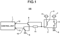
- FIG. 1 is a configuration diagram of a relay control device according to an embodiment of the present invention.
- a relay control device 100 includes a relay 2 including a coil 3 and a movable iron armature 4, a control unit 1 including a switching current output port 12 and a holding current output port 13 for controlling the operation of the movable iron armature 4, a switching current output transistor 9 connected with the switching current output port 12 of the control unit 1, a holding current output transistor 10 connected with the holding current output port 13 of the control unit 1, and a current limiting resistor 11 having one end connected with the holding current output transistor 10 and the other end connected with the switching current output transistor 9 and one end of the coil 3.
- the switching current output port 12 and the holding current output port 13 are digital output ports of the control unit 1.
- the switching current output transistor 9 controls current flowing through the coil 3 depending on a state of a signal output from the switching current output port 12.
- a signal output from the switching current output port 12 has a potential of two values, that is, a high level or a low level.
- the holding current output transistor 10 controls current flowing through the coil 3 depending on a state of a signal output from the holding current output port 13.
- a signal output from the holding current output port 13 has a potential of two values, that is, a high level or a low level.
- Examples of the switching current output transistor 9 and the holding current output transistor 10 include bipolar transistors, field effect transistors (FETs), metal oxide semiconductor field effect transistors (MOSFETs), insulated gate bipolar transistors (IGBTs) and insulated gate controlled thyristors (IGCTs).
- FETs field effect transistors
- MOSFETs metal oxide semiconductor field effect transistors
- IGBTs insulated gate bipolar transistors
- IGCTs insulated gate controlled thyristors
- npn bipolar transistors are used for the switching current output transistor 9 and the holding current output transistor 10.
- the collector of the switching current output transistor 9 is connected with the other end of the current limiting resistor 11 and with one end of the coil 3.
- the base of the switching current output transistor 9 is connected with the switching current output port 12.
- the emitter of the switching current output transistor 9 is connected with the emitter of the holding current output transistor 10 and with a primary side ground 6.
- the collector of the holding current output transistor 10 is connected with one end of the current limiting resistor 11.
- the base of the holding current output transistor 10 is connected with the holding current output port 13.
- the emitter of the holding current output transistor 10 is connected with the primary side ground 6 and with the emitter of the switching current output transistor 9.
- the other end of the coil 3 is connected with a primary side power supply 5.
- One end of the movable iron armature 4 is connected with a secondary side power supply 7.
- the other end of the movable iron armature 4 is connected with a secondary side ground 8.
- the coil 3 is excited when direct current supplied from the primary side power supply 5 flows to the primary side ground 6.
- the movable iron armature 4 is a normally-open movable component including a magnetic iron piece, and serves as a switch for opening and closing the secondary side power supply 7.
- the movable iron armature 4 has restoring force of restoring from a closed state to an open state. Note that the restoring force of the movable iron armature 4 is force produced by an elastic member such as a leaf spring or a coil spring.
- the secondary side circuit includes the movable iron armature 4, the secondary side power supply 7, and the secondary side ground 8. Description of elements constituting the secondary side circuit other than the movable iron armature 4, the secondary side power supply 7, and the secondary side ground 8 will be omitted.
- the value of current required for switching the movable iron armature 4 from the open state to the closed state and the value of current required for holding the closed state of the movable iron armature 4 after being switched to the closed state are different from each other.
- the current required for switching the movable iron armature 4 from the open state to the closed state will be referred to as switching current
- the current required for holding the closed state of the movable iron armature 4 after being switched to the closed state will be referred to as holding current.
- the value of the switching current is larger than that of the holding current, and required current amounts are specified in a product specification of the relay 2.
- excitation of the coil 3 is performed by two circuits, that is, a switching current output circuit constituted by the switching current output transistor 9 and a holding current output circuit constituted by the holding current output transistor 10 and the current limiting resistor 11.
- the presence and absence of current flowing between the collector and the emitter of the switching current output transistor 9 are switched by an output from the switching current output port 12.
- the output from the switching current output port 12 is set to the high level, current flows between the collector and the emitter of the switching current output transistor 9.
- current larger than the switching current specified in the product specification of the relay 2 flows through the coil 3.
- the current limiting resistor 11 is arranged in series between the holding current output transistor 10 and the coil 3. The presence and absence of current flowing between the collector and the emitter of the holding current output transistor 10 are switched by an output from the holding current output port 13. When the output from the holding current output port 13 is set to the high level, current flows between the collector and the emitter of the holding current output transistor 10.
- the amount of the aforementioned holding current can be adjusted by the current limiting resistor 11, and adjustment of the resistance depending on the model of the relay 2, for example, enables the relay control circuit to be mounted on various products.
- FIG. 2 is a flowchart of switching the relay illustrated in FIG. 1 from the open state to the closed state.
- FIG. 3 is a chart illustrating the output conditions of the switching current output port and holding current output port in association with the open/closed state of the relay illustrated in FIG. 1 when the relay is switched from the open state to the closed state.
- the relay 2 When the outputs from the switching current output port 12 and the holding current output port 13 are both set to the low level, the relay 2 is in the open state. At this point, when the control unit 1 is requested to start supply from the secondary side power supply (step S1), the control unit 1 sets the output of the holding current output port 13 to High (step S2).
- the control unit 1 measures the time that has elapsed from the time point when the output of the holding current output port 13 was set to the high level in step S2, and determines whether or not the time that has elapsed exceeds an inrush current settlement time T01 that is a first time, that is, whether or not the inrush current settlement time T01 has elapsed (step S3).
- step S3 When the inrush current settlement time T01 has not elapsed (step S3: No), the control unit 1 repeats the process in step S3.
- the inrush current settlement time T01 is assumed to be obtained from the time until the inrush current settles down; for example, when the time until the inrush current settles down is 1 [ms], the inrush current settlement time T01 is set to such a value as 100 [ms] with sufficient likelihood.
- the current limiting resistor 11 is provided in the holding current output circuit, the peak of the inrush current is lower and the time until the inrush current settles down is shorter than those in a case where the relay 2 is switched to the closed state by the switching current output circuit alone. This is because current is applied to the coil 3 via the current limiting resistor 11 of the holding current output circuit and then applied to the coil 3 via the switching current output circuit, which suppresses the magnitude of the inrush current as compared with a case where application of current to the coil 3 is started without the current limiting resistor 11.
- step S3 When the inrush current settlement time T01 has elapsed (step S3: Yes), the control unit 1 sets the output of the switching current output port 12 to the high level (step S4). At this point, the relay 2 is switched from the open state to the closed state, and power supply to the secondary side circuit is started.
- the control unit 1 measures the time that has elapsed from the time point when the output of the switching current output port 12 was set to the high level in step S4, and determines whether or not the time that has elapsed exceeds a switching current output time T02 that is a second time, that is, whether or not the switching current output time T02 has elapsed (step S5).
- step S5 No
- the control unit 1 repeats the process in step S5.
- the time for which the switching current needs to be continuously output for switching the relay 2 from the open state to the closed state is specified in a product specification.
- this time will be referred to as a switching stabilizing time T03.
- the switching current output time T02 is set to a time obtained from the switching stabilizing time T03 and consideration of likelihood. For example, when the switching stabilizing time T03 is 100 [ms], the switching current output time T02 is set to 10 [s], so that sufficient time is allowed for the relay 2 to be switched to the closed state.
- the control unit 1 can perform processes other than relay control while waiting for the switching current output time T02 to elapse.
- step S5 When the switching current output time T02 has elapsed (step S5: Yes), the control unit 1 sets the output of the switching current output port 12 to the low level (step S6). As a result of setting of the switching current output port 12 to the low level, the relay 2 is held in the closed state by the holding current (step S7).
- step S6 Because the current limiting resistor 11 is provided in the holding current output circuit, current flowing through the coil 3 is reduced. Specifically, the value of current flowing to the coil 3 and the holding current output transistor 10 via the current limiting resistor 11 is smaller than the value of current flowing to the coil 3 and the switching current output transistor 9 without passing through the current limiting resistor 11.
- the power consumed by the coil 3 while the relay 2 is held in the closed state by the holding current is smaller than that consumed by the coil 3 while the relay 2 is held in the closed state by switching holding current.
- FIG. 4 is a flowchart of switching the relay illustrated in FIG. 1 from the closed state to the open state.
- FIG. 5 is a chart illustrating the output conditions of the switching current output port and holding current output port in association with the open/closed state of the relay when the relay is switched from the closed state to the open state. Note that the state in which the relay 2 is held in the closed state by the holding current in step S7 described above is the initial state of the explanation of FIGS. 4 and 5 .
- step S11 When the control unit 1 is requested to stop supply from the secondary side power supply while the relay 2 is held in the closed state (step S11), the control unit 1 sets the outputs of the switching current output port 12 and the holding current output port 13 to the low level (step S12). Because current does not flow to the coil 3 any longer as a result of the setting in step S12, the magnetic force of the coil 3 is decreased, and the movable iron armature 4 is restored to the open state. As a result, power supply to the secondary side circuit is shut off.
- the relay 2 can be turned into the open state by the processes in the order in FIG. 4 .
- a specific example will be described with reference to FIGS. 6 and 7 .
- FIG. 6 is a chart illustrating the output conditions of the switching current output port and the holding current output port in association with the open/closed state of the relay when a request for stopping supply from the secondary side power supply occurs before the inrush current settlement time elapses.
- the control unit 1 sets the output of the holding current output port 13 to the low level. As a result, the relay 2 is maintained in the open state without being switched to the closed state.
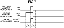
- FIG. 7 is a chart illustrating the output conditions of the switching current output port and the holding current output port in association with the open/closed state of the relay when a request for stopping supply from the secondary side power supply occurs before the switching current output time elapses.
- the control unit 1 sets the output of the switching current output port 12 to the low level.
- the relay 2 is switched from the closed state to the open state.
- Cited Document 1 the switching current output circuit controls opening and closing of a relay, and a large inrush current thus flows to the relay and relay peripheral circuit components arranged around the relay at switching current output. Circuit components with high absolute maximum rated current therefore need to be used for the relay and the relay peripheral circuit components. Because circuit components with high absolute maximum rated current are expensive, this is an obstacle to reduction in product cost.
- the relay control device 100 includes the coil 3, the movable iron armature 4 that is switched from the open state to the closed state when the coil 3 is excited, the switching current output transistor 9 that is the switching current output circuit that applies first current for switching the movable iron armature 4 from the open state to the closed state to the coil 3, and the holding current output transistor 10 that is the holding current output circuit that applies second current for holding the closed state of the movable iron armature 4 to the coil 3.
- the switching current output circuit is configured to apply the first current to the coil 3 when a first time has elapsed from when the second current started to be applied to the coil 3, the value of the second current being lower than that of the first current. According to this configuration, because the first current is applied to the coil 3 after the second current is applied to the coil 3, the peak value of the inrush current is low. Thus, circuit components with low absolute maximum rated current that are low in cost can be used.
- the relay control device 100 includes the switching current output circuit, and the holding current output circuit including the current limiting resistor 11 connected in series with the coil 3, the switching current output circuit applies the first current to the coil 3 from when the first time has elapsed until the second time elapses, and the second current is applied to the coil 3 and the current limiting resistor 11 instead of the first current after the second time has elapsed.
- the relay 2 is controlled by switching between two circuits, so that, after the relay 2 is switched to the closed state by the switching current output circuit, the closed state of the relay 2 is maintained only by the holding current output circuit. This configuration enables the power consumed by the coil 3 while the relay 2 is held in the closed state by the holding current to be smaller than that consumed by the coil 3 while the relay 2 is held in the closed state by switching holding current.
Landscapes
- Engineering & Computer Science (AREA)
- Power Engineering (AREA)
- Relay Circuits (AREA)
Abstract
Description
- The present invention relates to a relay control device that controls a mechanical relay.
-
Patent Literature 1 teaches a technology of intermittently outputting current for switching a relay, which is a mechanical relay, from an open state to a closed state to automatically restore the relay to the closed state in anticipation of a case where the closed state of a relay can no longer be held owing to instant voltage drop while current for holding the relay in the closed state is output. Hereinafter, the current output for holding the relay in the closed state will be referred to as holding current output, and the current output for switching the relay from the open state to the closed state will be referred to as switching current output. - Patent Literature 1: Japanese Patent No.
4378585 - The relay control method taught in
Patent Literature 1, however, has a problem in that components with high absolute maximum rated current need to be used for a relay and relay peripheral circuit components arranged around the relay because a large inrush current flows to the relay and the relay peripheral circuit components at the switching current output. - The present invention has been made in view of the above, and provides a relay control device capable of suppressing inrush current to a relay.
- To solve the aforementioned problems and achieve the object, a relay control device according to the present invention includes: a coil; a movable iron armature switched from an open state to a closed state when the coil is excited; a switching current output circuit to apply first current for switching the movable iron armature from the open state to the closed state to the coil; and a holding current output circuit to apply second current for holding the movable iron armature in the closed state to the coil. The switching current output circuit applies the first current to the coil when a first time has elapsed from when the second current started to be applied to the coil, and a value of the second current is lower than a value of the first current.
- A relay control device according to the present invention produces an effect of suppressing inrush current to a relay.
-
-
FIG. 1 is a configuration diagram of a relay control device according to an embodiment of the present invention. -
FIG. 2 is a flowchart of switching a relay illustrated inFIG. 1 from an open state to a closed state. -
FIG. 3 is a chart illustrating output conditions of the switching current output port and holding current output port in association with the open/closed state of the relay illustrated inFIG. 1 when the relay is switched from the open state to the closed state. -
FIG. 4 is a flowchart of switching the relay illustrated inFIG. 1 from the closed state to the open state. -
FIG. 5 is a chart illustrating output conditions of the switching current output port and holding current output port in association with the open/closed state of the relay when the relay is switched from the closed state to the open state. -
FIG. 6 is a chart illustrating the output conditions of the switching current output port and the holding current output port in association with the open/closed state of the relay when a request for stopping supply from the secondary side power supply occurs before the inrush current settlement time elapses. -
FIG. 7 is a chart illustrating the output conditions of the switching current output port and the holding current output port in association with the open/closed state of the relay when a request for stopping supply from the secondary side power supply occurs before the switching current output time elapses. - A relay control device according to an embodiment of the present invention will be described in detail below with reference to the drawings. Note that the present invention is not limited to the embodiment.
-
FIG. 1 is a configuration diagram of a relay control device according to an embodiment of the present invention. Arelay control device 100 according to the embodiment includes arelay 2 including acoil 3 and amovable iron armature 4, acontrol unit 1 including a switchingcurrent output port 12 and a holdingcurrent output port 13 for controlling the operation of themovable iron armature 4, a switchingcurrent output transistor 9 connected with the switchingcurrent output port 12 of thecontrol unit 1, a holdingcurrent output transistor 10 connected with the holdingcurrent output port 13 of thecontrol unit 1, and a current limitingresistor 11 having one end connected with the holdingcurrent output transistor 10 and the other end connected with the switchingcurrent output transistor 9 and one end of thecoil 3. - The switching
current output port 12 and the holdingcurrent output port 13 are digital output ports of thecontrol unit 1. - The switching
current output transistor 9 controls current flowing through thecoil 3 depending on a state of a signal output from the switchingcurrent output port 12. A signal output from the switchingcurrent output port 12 has a potential of two values, that is, a high level or a low level. - The holding
current output transistor 10 controls current flowing through thecoil 3 depending on a state of a signal output from the holdingcurrent output port 13. A signal output from the holdingcurrent output port 13 has a potential of two values, that is, a high level or a low level. - Examples of the switching
current output transistor 9 and the holdingcurrent output transistor 10 include bipolar transistors, field effect transistors (FETs), metal oxide semiconductor field effect transistors (MOSFETs), insulated gate bipolar transistors (IGBTs) and insulated gate controlled thyristors (IGCTs). In the present embodiment, npn bipolar transistors are used for the switchingcurrent output transistor 9 and the holdingcurrent output transistor 10. - The collector of the switching
current output transistor 9 is connected with the other end of the current limitingresistor 11 and with one end of thecoil 3. The base of the switchingcurrent output transistor 9 is connected with the switchingcurrent output port 12. The emitter of the switchingcurrent output transistor 9 is connected with the emitter of the holdingcurrent output transistor 10 and with aprimary side ground 6. - The collector of the holding
current output transistor 10 is connected with one end of the current limitingresistor 11. The base of the holdingcurrent output transistor 10 is connected with the holdingcurrent output port 13. The emitter of the holdingcurrent output transistor 10 is connected with theprimary side ground 6 and with the emitter of the switchingcurrent output transistor 9. - The other end of the
coil 3 is connected with a primary side power supply 5. One end of themovable iron armature 4 is connected with a secondary side power supply 7. The other end of themovable iron armature 4 is connected with asecondary side ground 8. - The
coil 3 is excited when direct current supplied from the primary side power supply 5 flows to theprimary side ground 6. Themovable iron armature 4 is a normally-open movable component including a magnetic iron piece, and serves as a switch for opening and closing the secondary side power supply 7. Themovable iron armature 4 has restoring force of restoring from a closed state to an open state. Note that the restoring force of themovable iron armature 4 is force produced by an elastic member such as a leaf spring or a coil spring. When current flows through thecoil 3 and thecoil 3 is thus excited, themovable iron armature 4 is attracted to thecoil 3 and switched from the open state to the closed state. In this process, the secondary side power supply 7 and thesecondary side ground 8 become electrically connected with each other, and power supply to circuit components of a secondary side circuit is started. The secondary side circuit includes themovable iron armature 4, the secondary side power supply 7, and thesecondary side ground 8. Description of elements constituting the secondary side circuit other than themovable iron armature 4, the secondary side power supply 7, and thesecondary side ground 8 will be omitted. - When the flow of direct current from the primary side power supply 5 to the
primary side ground 6 is stopped, the magnetic force generated in thecoil 3 is decreased, and themovable iron armature 4 is restored to the open state. Power supply to the secondary side circuit is thus shut off. - Typically, in the
relay 2, the value of current required for switching themovable iron armature 4 from the open state to the closed state and the value of current required for holding the closed state of themovable iron armature 4 after being switched to the closed state are different from each other. For convenience sake, the current required for switching themovable iron armature 4 from the open state to the closed state will be referred to as switching current, and the current required for holding the closed state of themovable iron armature 4 after being switched to the closed state will be referred to as holding current. The value of the switching current is larger than that of the holding current, and required current amounts are specified in a product specification of therelay 2. - In the present embodiment, excitation of the
coil 3 is performed by two circuits, that is, a switching current output circuit constituted by the switchingcurrent output transistor 9 and a holding current output circuit constituted by the holdingcurrent output transistor 10 and the current limitingresistor 11. - The presence and absence of current flowing between the collector and the emitter of the switching
current output transistor 9 are switched by an output from the switchingcurrent output port 12. When the output from the switchingcurrent output port 12 is set to the high level, current flows between the collector and the emitter of the switchingcurrent output transistor 9. For exciting thecoil 3 by the switching current output circuit, current larger than the switching current specified in the product specification of therelay 2 flows through thecoil 3. - The current limiting
resistor 11 is arranged in series between the holdingcurrent output transistor 10 and thecoil 3. The presence and absence of current flowing between the collector and the emitter of the holdingcurrent output transistor 10 are switched by an output from the holdingcurrent output port 13. When the output from the holdingcurrent output port 13 is set to the high level, current flows between the collector and the emitter of the holdingcurrent output transistor 10. - For exciting the
coil 3 by the holding current output circuit, current larger than the holding current specified in the product specification of therelay 2 and smaller than the switching current flows through thecoil 3. In this process, the amount of the aforementioned holding current can be adjusted by the current limitingresistor 11, and adjustment of the resistance depending on the model of therelay 2, for example, enables the relay control circuit to be mounted on various products. - Next, operation of the
relay control device 100 according to the present embodiment will be described.FIG. 2 is a flowchart of switching the relay illustrated inFIG. 1 from the open state to the closed state.FIG. 3 is a chart illustrating the output conditions of the switching current output port and holding current output port in association with the open/closed state of the relay illustrated inFIG. 1 when the relay is switched from the open state to the closed state. - When the outputs from the switching
current output port 12 and the holdingcurrent output port 13 are both set to the low level, therelay 2 is in the open state. At this point, when thecontrol unit 1 is requested to start supply from the secondary side power supply (step S1), thecontrol unit 1 sets the output of the holdingcurrent output port 13 to High (step S2). - The
control unit 1 measures the time that has elapsed from the time point when the output of the holdingcurrent output port 13 was set to the high level in step S2, and determines whether or not the time that has elapsed exceeds an inrush current settlement time T01 that is a first time, that is, whether or not the inrush current settlement time T01 has elapsed (step S3). - When the inrush current settlement time T01 has not elapsed (step S3: No), the
control unit 1 repeats the process in step S3. The inrush current settlement time T01 is assumed to be obtained from the time until the inrush current settles down; for example, when the time until the inrush current settles down is 1 [ms], the inrush current settlement time T01 is set to such a value as 100 [ms] with sufficient likelihood. - Because the current limiting
resistor 11 is provided in the holding current output circuit, the peak of the inrush current is lower and the time until the inrush current settles down is shorter than those in a case where therelay 2 is switched to the closed state by the switching current output circuit alone. This is because current is applied to thecoil 3 via the current limitingresistor 11 of the holding current output circuit and then applied to thecoil 3 via the switching current output circuit, which suppresses the magnitude of the inrush current as compared with a case where application of current to thecoil 3 is started without the current limitingresistor 11. - When the inrush current settlement time T01 has elapsed (step S3: Yes), the
control unit 1 sets the output of the switchingcurrent output port 12 to the high level (step S4). At this point, therelay 2 is switched from the open state to the closed state, and power supply to the secondary side circuit is started. - The
control unit 1 measures the time that has elapsed from the time point when the output of the switchingcurrent output port 12 was set to the high level in step S4, and determines whether or not the time that has elapsed exceeds a switching current output time T02 that is a second time, that is, whether or not the switching current output time T02 has elapsed (step S5). When the switching current output time T02 has not elapsed (step S5: No), thecontrol unit 1 repeats the process in step S5. - In a
typical relay 2, the time for which the switching current needs to be continuously output for switching therelay 2 from the open state to the closed state is specified in a product specification. Hereinafter, this time will be referred to as a switching stabilizing time T03. The switching current output time T02 is set to a time obtained from the switching stabilizing time T03 and consideration of likelihood. For example, when the switching stabilizing time T03 is 100 [ms], the switching current output time T02 is set to 10 [s], so that sufficient time is allowed for therelay 2 to be switched to the closed state. Note that thecontrol unit 1 can perform processes other than relay control while waiting for the switching current output time T02 to elapse. - When the switching current output time T02 has elapsed (step S5: Yes), the
control unit 1 sets the output of the switchingcurrent output port 12 to the low level (step S6). As a result of setting of the switchingcurrent output port 12 to the low level, therelay 2 is held in the closed state by the holding current (step S7). At this point, because the current limitingresistor 11 is provided in the holding current output circuit, current flowing through thecoil 3 is reduced. Specifically, the value of current flowing to thecoil 3 and the holdingcurrent output transistor 10 via the current limitingresistor 11 is smaller than the value of current flowing to thecoil 3 and the switchingcurrent output transistor 9 without passing through the current limitingresistor 11. Thus, the power consumed by thecoil 3 while therelay 2 is held in the closed state by the holding current is smaller than that consumed by thecoil 3 while therelay 2 is held in the closed state by switching holding current. -
FIG. 4 is a flowchart of switching the relay illustrated inFIG. 1 from the closed state to the open state.FIG. 5 is a chart illustrating the output conditions of the switching current output port and holding current output port in association with the open/closed state of the relay when the relay is switched from the closed state to the open state. Note that the state in which therelay 2 is held in the closed state by the holding current in step S7 described above is the initial state of the explanation ofFIGS. 4 and5 . - When the
control unit 1 is requested to stop supply from the secondary side power supply while therelay 2 is held in the closed state (step S11), thecontrol unit 1 sets the outputs of the switchingcurrent output port 12 and the holdingcurrent output port 13 to the low level (step S12). Because current does not flow to thecoil 3 any longer as a result of the setting in step S12, the magnetic force of thecoil 3 is decreased, and themovable iron armature 4 is restored to the open state. As a result, power supply to the secondary side circuit is shut off. - Note that, when a request for stopping supply from the secondary side power supply occurs between during the inrush current settlement time T01 or the switching current output time T02 as well, the
relay 2 can be turned into the open state by the processes in the order inFIG. 4 . A specific example will be described with reference toFIGS. 6 and7 . -
FIG. 6 is a chart illustrating the output conditions of the switching current output port and the holding current output port in association with the open/closed state of the relay when a request for stopping supply from the secondary side power supply occurs before the inrush current settlement time elapses. As illustrated inFIG. 6 , when a request for stopping supply from the secondary side power supply occurs before the inrush current settlement time T01 elapses, thecontrol unit 1 sets the output of the holdingcurrent output port 13 to the low level. As a result, therelay 2 is maintained in the open state without being switched to the closed state. -
FIG. 7 is a chart illustrating the output conditions of the switching current output port and the holding current output port in association with the open/closed state of the relay when a request for stopping supply from the secondary side power supply occurs before the switching current output time elapses. As illustrated inFIG. 7 , when a request for stopping supply from the secondary side power supply occurs before the switching current output time T02 elapses, thecontrol unit 1 sets the output of the switchingcurrent output port 12 to the low level. As a result, therelay 2 is switched from the closed state to the open state. - According to the related art typified by Cited
Document 1, the switching current output circuit controls opening and closing of a relay, and a large inrush current thus flows to the relay and relay peripheral circuit components arranged around the relay at switching current output. Circuit components with high absolute maximum rated current therefore need to be used for the relay and the relay peripheral circuit components. Because circuit components with high absolute maximum rated current are expensive, this is an obstacle to reduction in product cost. - The
relay control device 100 according to the present embodiment includes thecoil 3, themovable iron armature 4 that is switched from the open state to the closed state when thecoil 3 is excited, the switchingcurrent output transistor 9 that is the switching current output circuit that applies first current for switching themovable iron armature 4 from the open state to the closed state to thecoil 3, and the holdingcurrent output transistor 10 that is the holding current output circuit that applies second current for holding the closed state of themovable iron armature 4 to thecoil 3. In addition, the switching current output circuit is configured to apply the first current to thecoil 3 when a first time has elapsed from when the second current started to be applied to thecoil 3, the value of the second current being lower than that of the first current. According to this configuration, because the first current is applied to thecoil 3 after the second current is applied to thecoil 3, the peak value of the inrush current is low. Thus, circuit components with low absolute maximum rated current that are low in cost can be used. - In addition, the
relay control device 100 according to the present embodiment includes the switching current output circuit, and the holding current output circuit including the current limitingresistor 11 connected in series with thecoil 3, the switching current output circuit applies the first current to thecoil 3 from when the first time has elapsed until the second time elapses, and the second current is applied to thecoil 3 and the current limitingresistor 11 instead of the first current after the second time has elapsed. Thus, therelay 2 is controlled by switching between two circuits, so that, after therelay 2 is switched to the closed state by the switching current output circuit, the closed state of therelay 2 is maintained only by the holding current output circuit. This configuration enables the power consumed by thecoil 3 while therelay 2 is held in the closed state by the holding current to be smaller than that consumed by thecoil 3 while therelay 2 is held in the closed state by switching holding current. - The configurations presented in the embodiment above are examples of the present invention, which can be combined with other known technologies or can be partly omitted or modified without departing from the scope of the present invention.
- 1 control unit; 2 relay; 3 coil; 4 movable iron armature; 5 primary side power supply; 6 primary side ground; 7 secondary side power supply; 8 secondary side ground; 9 switching current output transistor; 10 holding current output transistor; 11 current limiting resistor; 12 switching current output port; 13 holding current output port; 100 relay control device.
Claims (2)
- A relay control device comprising:a coil;a movable iron armature switched from an open state to a closed state when the coil is excited;a switching current output circuit to apply first current for switching the movable iron armature from the open state to the closed state to the coil; anda holding current output circuit to apply second current for holding the movable iron armature in the closed state to the coil, whereinthe switching current output circuit applies the first current to the coil when a first time has elapsed from when the second current started to be applied to the coil, anda value of the second current is lower than a value of the first current.
- The relay control device according to claim 1, wherein
the holding current output circuit includes a resistor connected in series with the coil,
the switching current output circuit applies the first current to the coil from when the first time has elapsed until a second time elapses, and
the second current is applied to the coil and the resistor instead of the first current after the second time has elapsed.
Applications Claiming Priority (1)
| Application Number | Priority Date | Filing Date | Title |
|---|---|---|---|
| PCT/JP2017/017372 WO2018207231A1 (en) | 2017-05-08 | 2017-05-08 | Relay control device |
Publications (3)
| Publication Number | Publication Date |
|---|---|
| EP3624165A1 true EP3624165A1 (en) | 2020-03-18 |
| EP3624165A4 EP3624165A4 (en) | 2020-05-13 |
| EP3624165B1 EP3624165B1 (en) | 2024-07-10 |
Family
ID=64104471
Family Applications (1)
| Application Number | Title | Priority Date | Filing Date |
|---|---|---|---|
| EP17908987.5A Active EP3624165B1 (en) | 2017-05-08 | 2017-05-08 | Relay control device |
Country Status (6)
| Country | Link |
|---|---|
| US (1) | US11152176B2 (en) |
| EP (1) | EP3624165B1 (en) |
| JP (1) | JP6745988B2 (en) |
| CN (1) | CN110582827B (en) |
| AU (1) | AU2017413249B2 (en) |
| WO (1) | WO2018207231A1 (en) |
Families Citing this family (2)
| Publication number | Priority date | Publication date | Assignee | Title |
|---|---|---|---|---|
| EP3624165B1 (en) * | 2017-05-08 | 2024-07-10 | Mitsubishi Electric Corporation | Relay control device |
| CN110993441B (en) * | 2020-01-06 | 2023-04-25 | 广东美的制冷设备有限公司 | Control circuit, method, device, relay, home appliance and computer medium |
Family Cites Families (17)
| Publication number | Priority date | Publication date | Assignee | Title |
|---|---|---|---|---|
| JPS6058563B2 (en) * | 1978-06-23 | 1985-12-20 | 三菱電機株式会社 | solenoid drive circuit |
| JPH0346942U (en) * | 1989-09-14 | 1991-04-30 | ||
| US5085574A (en) * | 1989-10-12 | 1992-02-04 | Hamilton Standard Controls, Inc. | Fail-safe valve relay driver circuit for gas burners |
| US5210756A (en) * | 1990-09-26 | 1993-05-11 | Honeywell Inc. | Fault detection in relay drive circuits |
| US5568349A (en) * | 1995-04-04 | 1996-10-22 | Motorola, Inc. | Apparatus and method for controlling a relay device |
| JPH09306322A (en) * | 1996-05-16 | 1997-11-28 | Matsushita Electric Ind Co Ltd | Relay drive |
| US6236552B1 (en) * | 1996-11-05 | 2001-05-22 | Harness System Technologies Research, Ltd. | Relay drive circuit |
| JPH10255627A (en) * | 1997-03-12 | 1998-09-25 | Yazaki Corp | Relay drive circuit |
| JP2001091013A (en) | 1999-09-27 | 2001-04-06 | Matsushita Electric Ind Co Ltd | Control device for air conditioner |
| JP4378585B2 (en) | 2000-03-29 | 2009-12-09 | ソニー株式会社 | Relay drive device |
| JP2006294539A (en) * | 2005-04-14 | 2006-10-26 | Matsushita Electric Ind Co Ltd | Relay control device |
| KR20100032378A (en) * | 2007-05-18 | 2010-03-25 | 파나소닉 주식회사 | Relay driving circuit and battery pack using same |
| JP2009289671A (en) | 2008-05-30 | 2009-12-10 | Yazaki Corp | Relay control device |
| CN102664384B (en) * | 2012-05-02 | 2016-06-01 | 胡勇坚 | A kind of intelligent tripping method of power arrester |
| JP5920193B2 (en) | 2012-12-10 | 2016-05-18 | 株式会社オートネットワーク技術研究所 | Relay drive circuit |
| CN105006959B (en) * | 2015-07-27 | 2018-05-11 | 上海沪工焊接集团股份有限公司 | Inverter slow starting control circuit and control method |
| EP3624165B1 (en) * | 2017-05-08 | 2024-07-10 | Mitsubishi Electric Corporation | Relay control device |
-
2017
- 2017-05-08 EP EP17908987.5A patent/EP3624165B1/en active Active
- 2017-05-08 JP JP2019516749A patent/JP6745988B2/en not_active Expired - Fee Related
- 2017-05-08 AU AU2017413249A patent/AU2017413249B2/en not_active Ceased
- 2017-05-08 US US16/488,252 patent/US11152176B2/en active Active
- 2017-05-08 CN CN201780089177.5A patent/CN110582827B/en not_active Expired - Fee Related
- 2017-05-08 WO PCT/JP2017/017372 patent/WO2018207231A1/en not_active Ceased
Also Published As
| Publication number | Publication date |
|---|---|
| EP3624165B1 (en) | 2024-07-10 |
| CN110582827B (en) | 2021-08-20 |
| CN110582827A (en) | 2019-12-17 |
| AU2017413249A1 (en) | 2019-09-12 |
| AU2017413249B2 (en) | 2020-09-17 |
| JPWO2018207231A1 (en) | 2019-11-07 |
| US20200321177A1 (en) | 2020-10-08 |
| EP3624165A4 (en) | 2020-05-13 |
| US11152176B2 (en) | 2021-10-19 |
| JP6745988B2 (en) | 2020-08-26 |
| WO2018207231A1 (en) | 2018-11-15 |
Similar Documents
| Publication | Publication Date | Title |
|---|---|---|
| CN105788968B (en) | System and method for a freewheeling contactor circuit | |
| JP2020096525A (en) | Multi-stage gate-off switching with dynamic timing | |
| US10186857B2 (en) | Paralleling mechanical relays for increased current carrying and switching capacity | |
| JP6612972B2 (en) | Battery module | |
| US11152176B2 (en) | Relay control device | |
| CN205303336U (en) | Controlling means of contactor | |
| JP5676478B2 (en) | A system that accurately controls the operating characteristics of relays | |
| EP4080536B1 (en) | Contactor, and device and method for controlling same | |
| KR101546297B1 (en) | Circuit for an electromagnetic switching device | |
| CN102754176B (en) | Devices for electromagnetic switchgear | |
| TWI664656B (en) | Relay and method for controlling power supply | |
| JP2013106446A (en) | Transistor protection circuit | |
| CN106531555A (en) | Current limiting equipment and method | |
| CN204927187U (en) | Current -limiting equipment | |
| JP2004064863A (en) | Driving-device of motor | |
| US10593498B1 (en) | Circuit for reducing the power consumption when driving a relay | |
| JP2019186992A (en) | Power conversion device | |
| KR20170028041A (en) | Smart Power Relay Assembly | |
| JP2014090660A (en) | System and method for controlling electric motor | |
| CN205016473U (en) | Drive circuit of direct current coil | |
| JPH0855721A (en) | Dc-operated switch controller | |
| JP2001045752A (en) | Power supply |
Legal Events
| Date | Code | Title | Description |
|---|---|---|---|
| STAA | Information on the status of an ep patent application or granted ep patent |
Free format text: STATUS: THE INTERNATIONAL PUBLICATION HAS BEEN MADE |
|
| PUAI | Public reference made under article 153(3) epc to a published international application that has entered the european phase |
Free format text: ORIGINAL CODE: 0009012 |
|
| STAA | Information on the status of an ep patent application or granted ep patent |
Free format text: STATUS: REQUEST FOR EXAMINATION WAS MADE |
|
| 17P | Request for examination filed |
Effective date: 20191023 |
|
| AK | Designated contracting states |
Kind code of ref document: A1 Designated state(s): AL AT BE BG CH CY CZ DE DK EE ES FI FR GB GR HR HU IE IS IT LI LT LU LV MC MK MT NL NO PL PT RO RS SE SI SK SM TR |
|
| AX | Request for extension of the european patent |
Extension state: BA ME |
|
| A4 | Supplementary search report drawn up and despatched |
Effective date: 20200417 |
|
| RIC1 | Information provided on ipc code assigned before grant |
Ipc: H01H 47/04 20060101AFI20200409BHEP Ipc: H01H 47/10 20060101ALI20200409BHEP |
|
| DAV | Request for validation of the european patent (deleted) | ||
| DAX | Request for extension of the european patent (deleted) | ||
| STAA | Information on the status of an ep patent application or granted ep patent |
Free format text: STATUS: EXAMINATION IS IN PROGRESS |
|
| 17Q | First examination report despatched |
Effective date: 20220520 |
|
| GRAP | Despatch of communication of intention to grant a patent |
Free format text: ORIGINAL CODE: EPIDOSNIGR1 |
|
| STAA | Information on the status of an ep patent application or granted ep patent |
Free format text: STATUS: GRANT OF PATENT IS INTENDED |
|
| INTG | Intention to grant announced |
Effective date: 20240221 |
|
| GRAS | Grant fee paid |
Free format text: ORIGINAL CODE: EPIDOSNIGR3 |
|
| GRAA | (expected) grant |
Free format text: ORIGINAL CODE: 0009210 |
|
| STAA | Information on the status of an ep patent application or granted ep patent |
Free format text: STATUS: THE PATENT HAS BEEN GRANTED |
|
| AK | Designated contracting states |
Kind code of ref document: B1 Designated state(s): AL AT BE BG CH CY CZ DE DK EE ES FI FR GB GR HR HU IE IS IT LI LT LU LV MC MK MT NL NO PL PT RO RS SE SI SK SM TR |
|
| REG | Reference to a national code |
Ref country code: CH Ref legal event code: EP |
|
| REG | Reference to a national code |
Ref country code: DE Ref legal event code: R096 Ref document number: 602017083281 Country of ref document: DE |
|
| REG | Reference to a national code |
Ref country code: LT Ref legal event code: MG9D |
|
| REG | Reference to a national code |
Ref country code: NL Ref legal event code: MP Effective date: 20240710 |
|
| PG25 | Lapsed in a contracting state [announced via postgrant information from national office to epo] |
Ref country code: PT Free format text: LAPSE BECAUSE OF FAILURE TO SUBMIT A TRANSLATION OF THE DESCRIPTION OR TO PAY THE FEE WITHIN THE PRESCRIBED TIME-LIMIT Effective date: 20241111 |
|
| REG | Reference to a national code |
Ref country code: AT Ref legal event code: MK05 Ref document number: 1702808 Country of ref document: AT Kind code of ref document: T Effective date: 20240710 |
|
| PG25 | Lapsed in a contracting state [announced via postgrant information from national office to epo] |
Ref country code: NL Free format text: LAPSE BECAUSE OF FAILURE TO SUBMIT A TRANSLATION OF THE DESCRIPTION OR TO PAY THE FEE WITHIN THE PRESCRIBED TIME-LIMIT Effective date: 20240710 |
|
| PG25 | Lapsed in a contracting state [announced via postgrant information from national office to epo] |
Ref country code: PT Free format text: LAPSE BECAUSE OF FAILURE TO SUBMIT A TRANSLATION OF THE DESCRIPTION OR TO PAY THE FEE WITHIN THE PRESCRIBED TIME-LIMIT Effective date: 20241111 Ref country code: NL Free format text: LAPSE BECAUSE OF FAILURE TO SUBMIT A TRANSLATION OF THE DESCRIPTION OR TO PAY THE FEE WITHIN THE PRESCRIBED TIME-LIMIT Effective date: 20240710 |
|
| PG25 | Lapsed in a contracting state [announced via postgrant information from national office to epo] |
Ref country code: NO Free format text: LAPSE BECAUSE OF FAILURE TO SUBMIT A TRANSLATION OF THE DESCRIPTION OR TO PAY THE FEE WITHIN THE PRESCRIBED TIME-LIMIT Effective date: 20241010 |
|
| PG25 | Lapsed in a contracting state [announced via postgrant information from national office to epo] |
Ref country code: GR Free format text: LAPSE BECAUSE OF FAILURE TO SUBMIT A TRANSLATION OF THE DESCRIPTION OR TO PAY THE FEE WITHIN THE PRESCRIBED TIME-LIMIT Effective date: 20241011 Ref country code: FI Free format text: LAPSE BECAUSE OF FAILURE TO SUBMIT A TRANSLATION OF THE DESCRIPTION OR TO PAY THE FEE WITHIN THE PRESCRIBED TIME-LIMIT Effective date: 20240710 Ref country code: PL Free format text: LAPSE BECAUSE OF FAILURE TO SUBMIT A TRANSLATION OF THE DESCRIPTION OR TO PAY THE FEE WITHIN THE PRESCRIBED TIME-LIMIT Effective date: 20240710 |
|
| PG25 | Lapsed in a contracting state [announced via postgrant information from national office to epo] |
Ref country code: BG Free format text: LAPSE BECAUSE OF FAILURE TO SUBMIT A TRANSLATION OF THE DESCRIPTION OR TO PAY THE FEE WITHIN THE PRESCRIBED TIME-LIMIT Effective date: 20240710 |
|
| PG25 | Lapsed in a contracting state [announced via postgrant information from national office to epo] |
Ref country code: LV Free format text: LAPSE BECAUSE OF FAILURE TO SUBMIT A TRANSLATION OF THE DESCRIPTION OR TO PAY THE FEE WITHIN THE PRESCRIBED TIME-LIMIT Effective date: 20240710 |
|
| PG25 | Lapsed in a contracting state [announced via postgrant information from national office to epo] |
Ref country code: IS Free format text: LAPSE BECAUSE OF FAILURE TO SUBMIT A TRANSLATION OF THE DESCRIPTION OR TO PAY THE FEE WITHIN THE PRESCRIBED TIME-LIMIT Effective date: 20241110 Ref country code: AT Free format text: LAPSE BECAUSE OF FAILURE TO SUBMIT A TRANSLATION OF THE DESCRIPTION OR TO PAY THE FEE WITHIN THE PRESCRIBED TIME-LIMIT Effective date: 20240710 |
|
| PG25 | Lapsed in a contracting state [announced via postgrant information from national office to epo] |
Ref country code: HR Free format text: LAPSE BECAUSE OF FAILURE TO SUBMIT A TRANSLATION OF THE DESCRIPTION OR TO PAY THE FEE WITHIN THE PRESCRIBED TIME-LIMIT Effective date: 20240710 |
|
| PG25 | Lapsed in a contracting state [announced via postgrant information from national office to epo] |
Ref country code: ES Free format text: LAPSE BECAUSE OF FAILURE TO SUBMIT A TRANSLATION OF THE DESCRIPTION OR TO PAY THE FEE WITHIN THE PRESCRIBED TIME-LIMIT Effective date: 20240710 Ref country code: RS Free format text: LAPSE BECAUSE OF FAILURE TO SUBMIT A TRANSLATION OF THE DESCRIPTION OR TO PAY THE FEE WITHIN THE PRESCRIBED TIME-LIMIT Effective date: 20241010 |
|
| PG25 | Lapsed in a contracting state [announced via postgrant information from national office to epo] |
Ref country code: RS Free format text: LAPSE BECAUSE OF FAILURE TO SUBMIT A TRANSLATION OF THE DESCRIPTION OR TO PAY THE FEE WITHIN THE PRESCRIBED TIME-LIMIT Effective date: 20241010 Ref country code: PL Free format text: LAPSE BECAUSE OF FAILURE TO SUBMIT A TRANSLATION OF THE DESCRIPTION OR TO PAY THE FEE WITHIN THE PRESCRIBED TIME-LIMIT Effective date: 20240710 Ref country code: NO Free format text: LAPSE BECAUSE OF FAILURE TO SUBMIT A TRANSLATION OF THE DESCRIPTION OR TO PAY THE FEE WITHIN THE PRESCRIBED TIME-LIMIT Effective date: 20241010 Ref country code: LV Free format text: LAPSE BECAUSE OF FAILURE TO SUBMIT A TRANSLATION OF THE DESCRIPTION OR TO PAY THE FEE WITHIN THE PRESCRIBED TIME-LIMIT Effective date: 20240710 Ref country code: IS Free format text: LAPSE BECAUSE OF FAILURE TO SUBMIT A TRANSLATION OF THE DESCRIPTION OR TO PAY THE FEE WITHIN THE PRESCRIBED TIME-LIMIT Effective date: 20241110 Ref country code: HR Free format text: LAPSE BECAUSE OF FAILURE TO SUBMIT A TRANSLATION OF THE DESCRIPTION OR TO PAY THE FEE WITHIN THE PRESCRIBED TIME-LIMIT Effective date: 20240710 Ref country code: GR Free format text: LAPSE BECAUSE OF FAILURE TO SUBMIT A TRANSLATION OF THE DESCRIPTION OR TO PAY THE FEE WITHIN THE PRESCRIBED TIME-LIMIT Effective date: 20241011 Ref country code: FI Free format text: LAPSE BECAUSE OF FAILURE TO SUBMIT A TRANSLATION OF THE DESCRIPTION OR TO PAY THE FEE WITHIN THE PRESCRIBED TIME-LIMIT Effective date: 20240710 Ref country code: ES Free format text: LAPSE BECAUSE OF FAILURE TO SUBMIT A TRANSLATION OF THE DESCRIPTION OR TO PAY THE FEE WITHIN THE PRESCRIBED TIME-LIMIT Effective date: 20240710 Ref country code: BG Free format text: LAPSE BECAUSE OF FAILURE TO SUBMIT A TRANSLATION OF THE DESCRIPTION OR TO PAY THE FEE WITHIN THE PRESCRIBED TIME-LIMIT Effective date: 20240710 Ref country code: AT Free format text: LAPSE BECAUSE OF FAILURE TO SUBMIT A TRANSLATION OF THE DESCRIPTION OR TO PAY THE FEE WITHIN THE PRESCRIBED TIME-LIMIT Effective date: 20240710 |
|
| REG | Reference to a national code |
Ref country code: DE Ref legal event code: R097 Ref document number: 602017083281 Country of ref document: DE |
|
| PG25 | Lapsed in a contracting state [announced via postgrant information from national office to epo] |
Ref country code: SM Free format text: LAPSE BECAUSE OF FAILURE TO SUBMIT A TRANSLATION OF THE DESCRIPTION OR TO PAY THE FEE WITHIN THE PRESCRIBED TIME-LIMIT Effective date: 20240710 Ref country code: DK Free format text: LAPSE BECAUSE OF FAILURE TO SUBMIT A TRANSLATION OF THE DESCRIPTION OR TO PAY THE FEE WITHIN THE PRESCRIBED TIME-LIMIT Effective date: 20240710 Ref country code: RO Free format text: LAPSE BECAUSE OF FAILURE TO SUBMIT A TRANSLATION OF THE DESCRIPTION OR TO PAY THE FEE WITHIN THE PRESCRIBED TIME-LIMIT Effective date: 20240710 |
|
| PG25 | Lapsed in a contracting state [announced via postgrant information from national office to epo] |
Ref country code: EE Free format text: LAPSE BECAUSE OF FAILURE TO SUBMIT A TRANSLATION OF THE DESCRIPTION OR TO PAY THE FEE WITHIN THE PRESCRIBED TIME-LIMIT Effective date: 20240710 |
|
| PG25 | Lapsed in a contracting state [announced via postgrant information from national office to epo] |
Ref country code: CZ Free format text: LAPSE BECAUSE OF FAILURE TO SUBMIT A TRANSLATION OF THE DESCRIPTION OR TO PAY THE FEE WITHIN THE PRESCRIBED TIME-LIMIT Effective date: 20240710 |
|
| PG25 | Lapsed in a contracting state [announced via postgrant information from national office to epo] |
Ref country code: IT Free format text: LAPSE BECAUSE OF FAILURE TO SUBMIT A TRANSLATION OF THE DESCRIPTION OR TO PAY THE FEE WITHIN THE PRESCRIBED TIME-LIMIT Effective date: 20240710 Ref country code: SK Free format text: LAPSE BECAUSE OF FAILURE TO SUBMIT A TRANSLATION OF THE DESCRIPTION OR TO PAY THE FEE WITHIN THE PRESCRIBED TIME-LIMIT Effective date: 20240710 |
|
| PLBE | No opposition filed within time limit |
Free format text: ORIGINAL CODE: 0009261 |
|
| STAA | Information on the status of an ep patent application or granted ep patent |
Free format text: STATUS: NO OPPOSITION FILED WITHIN TIME LIMIT |
|
| 26N | No opposition filed |
Effective date: 20250411 |
|
| PG25 | Lapsed in a contracting state [announced via postgrant information from national office to epo] |
Ref country code: SE Free format text: LAPSE BECAUSE OF FAILURE TO SUBMIT A TRANSLATION OF THE DESCRIPTION OR TO PAY THE FEE WITHIN THE PRESCRIBED TIME-LIMIT Effective date: 20240710 |
|
| REG | Reference to a national code |
Ref country code: DE Ref legal event code: R119 Ref document number: 602017083281 Country of ref document: DE |
|
| REG | Reference to a national code |
Ref country code: CH Ref legal event code: H13 Free format text: ST27 STATUS EVENT CODE: U-0-0-H10-H13 (AS PROVIDED BY THE NATIONAL OFFICE) Effective date: 20251223 |
|
| PG25 | Lapsed in a contracting state [announced via postgrant information from national office to epo] |
Ref country code: LU Free format text: LAPSE BECAUSE OF NON-PAYMENT OF DUE FEES Effective date: 20250508 |
|
| PG25 | Lapsed in a contracting state [announced via postgrant information from national office to epo] |
Ref country code: CH Free format text: LAPSE BECAUSE OF NON-PAYMENT OF DUE FEES Effective date: 20250531 |
|
| GBPC | Gb: european patent ceased through non-payment of renewal fee |
Effective date: 20250508 |
|
| REG | Reference to a national code |
Ref country code: BE Ref legal event code: MM Effective date: 20250531 |
|
| PG25 | Lapsed in a contracting state [announced via postgrant information from national office to epo] |
Ref country code: MC Free format text: LAPSE BECAUSE OF FAILURE TO SUBMIT A TRANSLATION OF THE DESCRIPTION OR TO PAY THE FEE WITHIN THE PRESCRIBED TIME-LIMIT Effective date: 20240710 |
|
| PG25 | Lapsed in a contracting state [announced via postgrant information from national office to epo] |
Ref country code: GB Free format text: LAPSE BECAUSE OF NON-PAYMENT OF DUE FEES Effective date: 20250508 |
|
| PG25 | Lapsed in a contracting state [announced via postgrant information from national office to epo] |
Ref country code: IE Free format text: LAPSE BECAUSE OF NON-PAYMENT OF DUE FEES Effective date: 20250508 Ref country code: DE Free format text: LAPSE BECAUSE OF NON-PAYMENT OF DUE FEES Effective date: 20251202 |
|
| PG25 | Lapsed in a contracting state [announced via postgrant information from national office to epo] |
Ref country code: BE Free format text: LAPSE BECAUSE OF NON-PAYMENT OF DUE FEES Effective date: 20250531 |
|
| PG25 | Lapsed in a contracting state [announced via postgrant information from national office to epo] |
Ref country code: FR Free format text: LAPSE BECAUSE OF NON-PAYMENT OF DUE FEES Effective date: 20250531 |