EP3624100A1 - Light emitting control circuit, light emitting control driver and display device - Google Patents
Light emitting control circuit, light emitting control driver and display device Download PDFInfo
- Publication number
- EP3624100A1 EP3624100A1 EP18901277.6A EP18901277A EP3624100A1 EP 3624100 A1 EP3624100 A1 EP 3624100A1 EP 18901277 A EP18901277 A EP 18901277A EP 3624100 A1 EP3624100 A1 EP 3624100A1
- Authority
- EP
- European Patent Office
- Prior art keywords
- thin film
- film transistor
- emission control
- control unit
- signal
- Prior art date
- Legal status (The legal status is an assumption and is not a legal conclusion. Google has not performed a legal analysis and makes no representation as to the accuracy of the status listed.)
- Granted
Links
Images

Classifications
-
- G—PHYSICS
- G09—EDUCATION; CRYPTOGRAPHY; DISPLAY; ADVERTISING; SEALS
- G09G—ARRANGEMENTS OR CIRCUITS FOR CONTROL OF INDICATING DEVICES USING STATIC MEANS TO PRESENT VARIABLE INFORMATION
- G09G3/00—Control arrangements or circuits, of interest only in connection with visual indicators other than cathode-ray tubes
- G09G3/20—Control arrangements or circuits, of interest only in connection with visual indicators other than cathode-ray tubes for presentation of an assembly of a number of characters, e.g. a page, by composing the assembly by combination of individual elements arranged in a matrix no fixed position being assigned to or needed to be assigned to the individual characters or partial characters
- G09G3/22—Control arrangements or circuits, of interest only in connection with visual indicators other than cathode-ray tubes for presentation of an assembly of a number of characters, e.g. a page, by composing the assembly by combination of individual elements arranged in a matrix no fixed position being assigned to or needed to be assigned to the individual characters or partial characters using controlled light sources
- G09G3/30—Control arrangements or circuits, of interest only in connection with visual indicators other than cathode-ray tubes for presentation of an assembly of a number of characters, e.g. a page, by composing the assembly by combination of individual elements arranged in a matrix no fixed position being assigned to or needed to be assigned to the individual characters or partial characters using controlled light sources using electroluminescent panels
- G09G3/32—Control arrangements or circuits, of interest only in connection with visual indicators other than cathode-ray tubes for presentation of an assembly of a number of characters, e.g. a page, by composing the assembly by combination of individual elements arranged in a matrix no fixed position being assigned to or needed to be assigned to the individual characters or partial characters using controlled light sources using electroluminescent panels semiconductive, e.g. using light-emitting diodes [LED]
-
- G—PHYSICS
- G09—EDUCATION; CRYPTOGRAPHY; DISPLAY; ADVERTISING; SEALS
- G09G—ARRANGEMENTS OR CIRCUITS FOR CONTROL OF INDICATING DEVICES USING STATIC MEANS TO PRESENT VARIABLE INFORMATION
- G09G3/00—Control arrangements or circuits, of interest only in connection with visual indicators other than cathode-ray tubes
- G09G3/20—Control arrangements or circuits, of interest only in connection with visual indicators other than cathode-ray tubes for presentation of an assembly of a number of characters, e.g. a page, by composing the assembly by combination of individual elements arranged in a matrix no fixed position being assigned to or needed to be assigned to the individual characters or partial characters
-
- G—PHYSICS
- G09—EDUCATION; CRYPTOGRAPHY; DISPLAY; ADVERTISING; SEALS
- G09G—ARRANGEMENTS OR CIRCUITS FOR CONTROL OF INDICATING DEVICES USING STATIC MEANS TO PRESENT VARIABLE INFORMATION
- G09G3/00—Control arrangements or circuits, of interest only in connection with visual indicators other than cathode-ray tubes
- G09G3/20—Control arrangements or circuits, of interest only in connection with visual indicators other than cathode-ray tubes for presentation of an assembly of a number of characters, e.g. a page, by composing the assembly by combination of individual elements arranged in a matrix no fixed position being assigned to or needed to be assigned to the individual characters or partial characters
- G09G3/22—Control arrangements or circuits, of interest only in connection with visual indicators other than cathode-ray tubes for presentation of an assembly of a number of characters, e.g. a page, by composing the assembly by combination of individual elements arranged in a matrix no fixed position being assigned to or needed to be assigned to the individual characters or partial characters using controlled light sources
- G09G3/30—Control arrangements or circuits, of interest only in connection with visual indicators other than cathode-ray tubes for presentation of an assembly of a number of characters, e.g. a page, by composing the assembly by combination of individual elements arranged in a matrix no fixed position being assigned to or needed to be assigned to the individual characters or partial characters using controlled light sources using electroluminescent panels
- G09G3/32—Control arrangements or circuits, of interest only in connection with visual indicators other than cathode-ray tubes for presentation of an assembly of a number of characters, e.g. a page, by composing the assembly by combination of individual elements arranged in a matrix no fixed position being assigned to or needed to be assigned to the individual characters or partial characters using controlled light sources using electroluminescent panels semiconductive, e.g. using light-emitting diodes [LED]
- G09G3/3208—Control arrangements or circuits, of interest only in connection with visual indicators other than cathode-ray tubes for presentation of an assembly of a number of characters, e.g. a page, by composing the assembly by combination of individual elements arranged in a matrix no fixed position being assigned to or needed to be assigned to the individual characters or partial characters using controlled light sources using electroluminescent panels semiconductive, e.g. using light-emitting diodes [LED] organic, e.g. using organic light-emitting diodes [OLED]
- G09G3/3266—Details of drivers for scan electrodes
-
- G—PHYSICS
- G09—EDUCATION; CRYPTOGRAPHY; DISPLAY; ADVERTISING; SEALS
- G09G—ARRANGEMENTS OR CIRCUITS FOR CONTROL OF INDICATING DEVICES USING STATIC MEANS TO PRESENT VARIABLE INFORMATION
- G09G3/00—Control arrangements or circuits, of interest only in connection with visual indicators other than cathode-ray tubes
- G09G3/20—Control arrangements or circuits, of interest only in connection with visual indicators other than cathode-ray tubes for presentation of an assembly of a number of characters, e.g. a page, by composing the assembly by combination of individual elements arranged in a matrix no fixed position being assigned to or needed to be assigned to the individual characters or partial characters
- G09G3/34—Control arrangements or circuits, of interest only in connection with visual indicators other than cathode-ray tubes for presentation of an assembly of a number of characters, e.g. a page, by composing the assembly by combination of individual elements arranged in a matrix no fixed position being assigned to or needed to be assigned to the individual characters or partial characters by control of light from an independent source
-
- G—PHYSICS
- G11—INFORMATION STORAGE
- G11C—STATIC STORES
- G11C19/00—Digital stores in which the information is moved stepwise, e.g. shift registers
- G11C19/28—Digital stores in which the information is moved stepwise, e.g. shift registers using semiconductor elements
-
- G—PHYSICS
- G09—EDUCATION; CRYPTOGRAPHY; DISPLAY; ADVERTISING; SEALS
- G09G—ARRANGEMENTS OR CIRCUITS FOR CONTROL OF INDICATING DEVICES USING STATIC MEANS TO PRESENT VARIABLE INFORMATION
- G09G2310/00—Command of the display device
- G09G2310/02—Addressing, scanning or driving the display screen or processing steps related thereto
- G09G2310/0264—Details of driving circuits
- G09G2310/0286—Details of a shift registers arranged for use in a driving circuit
-
- G—PHYSICS
- G09—EDUCATION; CRYPTOGRAPHY; DISPLAY; ADVERTISING; SEALS
- G09G—ARRANGEMENTS OR CIRCUITS FOR CONTROL OF INDICATING DEVICES USING STATIC MEANS TO PRESENT VARIABLE INFORMATION
- G09G2310/00—Command of the display device
- G09G2310/08—Details of timing specific for flat panels, other than clock recovery
-
- G—PHYSICS
- G09—EDUCATION; CRYPTOGRAPHY; DISPLAY; ADVERTISING; SEALS
- G09G—ARRANGEMENTS OR CIRCUITS FOR CONTROL OF INDICATING DEVICES USING STATIC MEANS TO PRESENT VARIABLE INFORMATION
- G09G2320/00—Control of display operating conditions
- G09G2320/06—Adjustment of display parameters
- G09G2320/0626—Adjustment of display parameters for control of overall brightness
- G09G2320/064—Adjustment of display parameters for control of overall brightness by time modulation of the brightness of the illumination source
-
- G—PHYSICS
- G09—EDUCATION; CRYPTOGRAPHY; DISPLAY; ADVERTISING; SEALS
- G09G—ARRANGEMENTS OR CIRCUITS FOR CONTROL OF INDICATING DEVICES USING STATIC MEANS TO PRESENT VARIABLE INFORMATION
- G09G2330/00—Aspects of power supply; Aspects of display protection and defect management
- G09G2330/02—Details of power systems and of start or stop of display operation
- G09G2330/021—Power management, e.g. power saving
Definitions
- Embodiments of the present application relate to the field of display technologies, and more specifically to an emission control circuit, an emission control driver and a display device.
- a display device may include a plurality of pixels, a data driver, a scan driver, and an emission control driver.
- the plurality of pixels are configured to display an image
- the data driver is configured to provide data voltages to the pixels
- the scan driver is configured to provide scanning signals to the pixels
- the emission control driver is configured to provide emission control signals to the pixels
- the emission control signals may control emission time of the pixels.
- the emission control driver may include multiple-stages of emission control circuits, each of which may be configured to control emission time of a row of the pixels.
- one stage of emission control circuit which may include a plurality of thin film transistors, an initial signal, and a plurality of clock signals, may control the thin film transistors to be in on-state or off-state, so that the emission control circuit can output the emission control signals.
- each stage of emission control circuit includes a large number of thin film transistors (usually more than 20), resulting in a complicated emission control circuit.
- an emission control circuit is provided in embodiments of the present application, and the circuit includes less thin film transistors and has a simple structure, to achieve requirements of simplifying a structure of the emitting control circuit.
- an emission control circuit is provided by the embodiments of the present application, and the emission control circuit includes a first control unit, a second control unit and an emission control unit.
- the first control unit configured to output a first control signal is respectively connected to an initial signal line, a first clock signal line and a first power source.
- the second control unit an output terminal of which is respectively connected to a terminal of the first control unit, a second clock signal line and a second power source, is configured to output a second control signal.
- the emission control unit an output terminal of which is respectively connected to the first control unit, the second control unit, the first power source and the second power source, is configured to output an emission control signal under control of the first control signal and the second control signal.
- the emission control unit includes a ninth thin film transistor, a tenth thin film transistor, a second capacitor, and a third capacitor.
- a source of the ninth thin film transistor is connected to the second power source, a drain of the ninth thin film transistor is connected to a source of the tenth thin film transistor, and a gate of the ninth thin film transistor is connected to the output terminal, configured to output the second control signal, of the second control unit.
- a drain of the tenth thin film transistor is connected to the first power source, and a gate of the tenth thin film transistor is connected to the output terminal, configured to output the first control signal, of the first control unit.
- a terminal of the second capacitor is connected to an output terminal, configured to output the second control signal, of the second control unit, and another terminal of the second capacitor is connected to the second power source.
- a terminal of the third capacitor is connected to the second clock signal line, and another terminal of the third capacitor is connected to an output terminal, configured to output the first control signal, of the first control unit.
- the drain of the ninth thin film transistor or the source of the tenth thin film transistor is an output terminal of the emission control unit, and a signal output by the drain of the ninth thin film transistor or the source of the tenth thin film transistor is the emission control signal.
- the tenth thin film transistor is controlled by the first control signal to be in on-state or off-state
- the ninth thin film transistor is controlled by the second control signal to be in on-state or off-state.
- the ninth thin film transistor when the tenth thin film transistor is controlled by the first control signal to be in on-state, the ninth thin film transistor is controlled by the second control signal to be in off-state ; and, when the tenth thin film transistor is controlled by the first control signal to be in off-state, the ninth thin film transistor is controlled by the second control signal to be in on-state.
- the emission control signal is a voltage output by the first power source.
- the emission control signal is a voltage output by the second power source.
- the first control unit includes a first thin film transistor, a second thin film transistor, and a third thin film transistor.
- a gate of the first thin film transistor is respectively connected to a source of the second thin film transistor, a gate of the third thin film transistor, and the first clock signal line, a drain of the first thin film transistor is connected to the initial signal line, and a source of the first thin film transistor is connected to a gate of the second thin film transistor; a drain of the second thin film transistor is connected to a source of the third thin film transistor; a drain of the third thin film transistor is connected to the first power source; and, the source of the first thin film transistor is the output terminal of the first control unit, and a signal output by the output terminal of the first control unit is the first control signal.
- the second control unit includes a fourth thin film transistor, a fifth thin film transistor, a sixth thin film transistor, a seventh thin film transistor, an eighth thin film transistor, and a first capacitor; wherein, a gate of the fourth thin film transistor is respectively connected to a gate of the sixth thin film transistor and a terminal of the first capacitor, a source of the fourth thin film transistor is connected to a source of the fifth thin film transistor, and a drain of the fourth thin film transistor is respectively connected to a drain of the eighth thin film transistor and the second power source; a gate of the fifth thin film transistor is respectively connected to the second clock signal line, a drain of the sixth thin film transistor, a gate of the seventh thin film transistor, and another terminal of the first capacitor, and a drain of the fifth thin film transistor is respectively connected to a gate of the eighth thin film transistor and a source of the first thin film transistor; a source of the sixth thin film transistor is connected to a source of the seventh thin film transistor, and a drain of the seventh thin film transistor is connected to a source of the first capacitor;
- the initial signal line is configured to provide an initial signal
- the first clock signal line is configured to provide a first clock signal
- the second clock signal line is configured to provide a second clock signal
- a voltage output by the first power source is a negative voltage
- a voltage output by the second power source is a positive voltage
- the first thin film transistor, the second thin film transistor, the third thin film transistor, the fourth thin film transistor, the fifth thin film transistor, the sixth thin film transistor, the seventh thin film transistor, the eighth thin film transistor, the ninth thin film transistor, and the tenth thin film transistor are all P-type thin film transistors.
- At least one thin film transistor of the first thin film transistor, the second thin film transistor, the third thin film transistor, the fourth thin film transistor, the fifth thin film transistor, the sixth thin film transistor, the seventh thin film transistor, the eighth thin film transistor, the ninth thin film transistor, and the tenth thin film transistor is an N-type thin film transistor.
- an emission control driver is also provided by the embodiments of the present application, and the emission control driver includes at least two stages of emission control circuits described above.
- an signal input to a first stage emission control circuit is an initial signal, and an emission control signal output by a (n-1) th stage emission control circuit is used as an initial signal of a n th stage emission control circuit; and a first clock signal input to the (n-1) th stage emission control circuit is used as a second clock signal input to the n th stage emission control circuit, and a second clock signal input to the (n-1) th stage emission control circuit is used as a first clock signal input to the nth stage emission control circuit, and n is an integer greater than 1.
- a display device is also provided by the embodiments of the present application, and the display device includes the emission control driver described above.
- the emission control circuit includes the first control unit, the second control unit, and the emission control unit.
- the input terminal of the first control unit configured to output the first control signal is respectively connected to the initial signal line, the first clock signal line and the first power source
- the input terminal of the second control unit configured to output the second control signal is respectively connected to the first control unit, the second clock signal line and the second power source
- an input terminal of the emission control unit is respectively connected to the first control unit, the second control unit, the first power source and the second power source
- an output of the emission control unit is configured to output an emission control signal under control of the first control signal and the second control signal.
- the emission control signal output by the emission control circuit according to the embodiments of the present application may control pixels to emit light, and the circuit structure of the emission control circuit is relatively simple.
- a first thin film transistor, a second thin film transistor, a third thin film transistor, a fourth thin film transistor, a fifth thin film transistor, a sixth thin film transistor, a seventh thin film transistor, an eighth thin film transistor, a ninth thin film transistor, and a tenth thin film transistor may all be N-type thin film transistors, or all be P-type thin film transistors.
- at least one of the transistors may be N-type thin film transistors, and the rest of the transistors are P-type thin film transistors, which is not specifically limited herein.
- FIG. 1 is a schematic structural diagram of an emission control circuit according to an embodiment of the present application.
- the emission control circuit can generate an emission control signal that can control emission time of pixels.
- the emission control circuit is described below.
- the emission control circuit may include: a first control unit 11, a second control unit 12, and an emission control unit 13.
- An input terminal of the first control unit 11 may be respectively connected to an initial signal line, a first clock signal line, and a first power source VGL.
- the initial signal line may provide an initial signal EIN
- the first clock signal line may provide a first clock signal CK1
- the first clock signal CK1 may be a pulse signal
- the first power source VGL may has a negative voltage, i.e., the first power source VGL may output a low level.
- the first control unit 11 may be configured to output a first control signal under control of the initial signal EIN, the first clock signal CK1, and the first power source VGL.
- An input terminal of the second control unit 12 may be respectively connected to the first control unit 11, a second clock signal line, and a second power source VGH.
- the second clock signal line may provide a second clock signal CK2, and the second clock signal CK2 may also be a pulse signal.
- the second power source VGH may have a positive voltage, i.e., the second power source VGH may output a high level.
- the second control unit 12 may be configured to output a second control signal under control of the first control unit 11, the second clock signal CK2, and the second power source VGH.
- An input terminal of the emission control unit 13 may be respectively connected to the first control unit 11, the second control unit 12, the first power source VGL and the second power source VGH.
- the first control signal and the second control signal may be input to the emission control unit 13, and the emission control unit 13 may be configured to output an emission control signal EM under control of the first control signal and the second control signal.
- the emission control unit may output the emission control signal under control of the first control unit, the second control unit, the clock signal, and the voltage of the power source, and the emission control signal may control the emission time of the pixels.
- the emission control unit 13 may include: a ninth thin film transistor M9, a tenth thin film transistor M10, a second capacitor C2, and a third capacitor C3.
- a source of the ninth thin film transistor M9 is connected to the second power source VGH, a drain of the ninth thin film transistor M9 is connected to a source of the tenth thin film transistor M10, and a gate of the ninth thin film transistor M9 is connected to the output terminal, configured to output the second control signal, of the second control unit 12.
- a drain of the tenth thin film transistor M10 is connected to the first power source VGL, and a gate of the tenth thin film transistor M10 is connected to the output terminal, configured to output the first control signal, of the first control unit 11.
- a terminal of the second capacitor C2 is connected to the output terminal, configured to output the second control signal, of the second control unit 12, and another terminal of the second capacitor C2 is connected to the second power source VGH.
- a terminal of the third capacitor C3 is connected to the second clock signal CK2, and another terminal of the third capacitor C3 is connected to the output terminal, configured to output the first control signal, of the first control unit 11.
- the drain of the ninth thin film transistor M9 or the source of the tenth thin film transistor M10 is the output terminal of the emission control unit 13, and a signal output by the drain of the ninth thin film transistor M9 or the source of the tenth thin film transistor M10 is the emission control signal.
- the first control unit 11 shown in FIG. 1 may include: a first thin film transistor, a second thin film transistor, and a third thin film transistor.
- the second control unit 12 shown in FIG. 1 may include: a fourth thin film transistor, a fifth thin film transistor, a sixth thin film transistor, a seventh thin film transistor, an eighth thin film transistor, and a capacitor.
- FIG. 2 is a schematic structural diagram of an emission control circuit according to another embodiment of the present application.
- the first control unit 11 includes a first thin film transistor M1, a second thin film transistor M2, and a third thin film transistor M3.
- the second control unit 12 includes a fourth thin film transistor M4, a fifth thin film transistor M5, a sixth thin film transistor M6, a seventh thin film transistor M7, an eighth thin film transistor M8, and a first capacitor C1.
- the emission control unit 13 includes a ninth thin film transistor M9, a tenth thin film transistor M10, a second capacitor C2, and a third capacitor C3.
- the thin film transistors, shown in FIG. 2 are all P-type thin film transistors.
- the circuit structure of the emission control circuit shown in FIG. 2 is as follows.
- a gate of the first thin film transistor M1 is respectively connected to a source of the second thin film transistor M2, a gate of the third thin film transistor M3 and the first clock signal line, a drain of the first thin film transistor M1 is connected to the initial signal line, and a source of the first thin film transistor M1 is respectively connected to a gate of the second thin film transistor M2, a drain of the fifth thin film transistor M5, a gate of the eighth thin film transistor M8, a gate of the tenth thin film transistor M10 and one terminal of the third capacitor C3 (a first node N1 shown in FIG. 2 ).
- a drain of the second thin film transistor M2 is connected to a source of the third thin film transistor M3.
- a drain of the third thin film transistor M3 is connected to the first power source VGL.
- a gate of the fourth thin film transistor M4 is respectively connected to a gate of the sixth thin film transistor M6 and one terminal of the first capacitor C1 (a second node N2 shown in FIG. 2 ), and a source of the fourth thin film transistor M4 is connected to a source of the fifth thin film M5, and a drain of the fourth thin film transistor M4 is respectively connected to a drain of the eighth thin film transistor M8 and the second power source VGH.
- a gate of the fifth thin film transistor M5 is respectively connected to the second clock signal line, a drain of the sixth thin film transistor M6, a gate of the seventh thin film transistor M7, another terminal of the first capacitor C1, and another terminal of the third capacitor C3.
- a source of the sixth thin film transistor M6 is connected to a source of the seventh thin film transistor M7.
- a drain of the seventh thin film transistor M7 is respectively connected to a source of the eighth thin film transistor M8, a gate of the ninth thin film transistor M9, and a terminal of the second capacitor C2 (a third node N3 shown in FIG. 2 ).
- a source of the ninth thin film transistor M9 is respectively connected to the second power source VGH and another terminal of the second capacitor C2, and a drain of the ninth thin film transistor M9 is connected to a source of the tenth thin film transistor M10.
- a drain of the tenth thin film transistor M10 is connected to the first power source VGL.
- a signal output by the source of the first thin film transistor M1 (i.e., the first node N1 shown in FIG. 2 ) may be regarded as the first control signal;
- a signal output by the source of the eighth thin film transistor M8 (i.e., the third node N3 shown in FIG. 2 ) may be regarded as the second control signal;
- a signal output by the drain of the ninth thin film transistor M9 (or the source of the tenth thin film transistor M10) may be regarded as the emission control signal EM.
- the first control signal may be output to the gate of the tenth thin film transistor M10 and the tenth thin film transistor M10 is controlled by the first control signal to be in on-state or off-state; the second control signal may be output to the gate of the ninth thin film transistor M9 and the ninth thin film transistor M9 is controlled by the second control signal to be in on-state or off-state.
- the emission control signal EM may be output to pixels and the emission control signal EM is configured to control emission time of the pixels.
- first thin film transistor M1 the second thin film transistor M2, the third thin film transistor M3, the fourth thin film transistor M4, the fifth thin film transistor M5, the sixth thin film transistor M6, the seventh thin film transistor M7, the eighth thin film transistor M8, the ninth thin film transistor M9 and the tenth thin film transistor M10, may be selected according to a practical application.
- the first thin film transistor M1, the second thin film transistor M2, the third thin film transistor M3, the fourth thin film transistor M4, the fifth thin film transistor M5, the sixth thin film transistor M6, the seventh thin film transistor M7, the eighth thin film transistor M8, the ninth thin film transistor M9 and the tenth thin film transistor M10 may all be the P-type thin film transistor as described above, or at least one thin film transistor of the first thin film transistor M1, the second thin film transistor M2, the third thin film transistor M3, the fourth thin film transistor M4, the fifth thin film transistor M5, the sixth thin film transistor M6, the seventh thin film transistor M7, the eighth thin film transistor M8, the ninth thin film transistor M9 and the tenth thin film transistor M10 is the N-type thin film transistor.
- the first capacitor C1 and the third capacitor C3 may be bootstrap capacitors configured to raise or lower a level of a node
- the second capacitor C2 may be a storage capacitor configured to maintain the level of the node.
- One terminal of the first capacitor C1 i.e., the second node N2 shown in FIG. 2
- the gate of the fourth thin film transistor M4 and the gate of the sixth thin film transistor M6 is respectively connected to the gate of the fourth thin film transistor M4 and the gate of the sixth thin film transistor M6, and another terminal of the first capacitor C1 is connected to the second clock signal line.
- the first capacitor C1 may be configured to raise or lower a level of the second node N2, and thereby the fourth thin film transistor M4 and the sixth thin film transistor M6 are controlled to be in on-state or off-state.
- One terminal of the second capacitor C2 (i.e., the third node N3 shown in FIG. 2 ) is respectively connected to the source of the eighth thin film transistor M8 and the gate of the ninth thin film transistor M9, and another terminal of the second capacitor C2 is connected to the second power source VGH.
- the eighth thin film transistor M8 is in on-state, a voltage of the third node N3 is a high level, and when the eighth thin film transistor M8 is turned from being in on-state to being in off-state, since the second capacitor C2 is the storage capacitor, the second capacitor C2 may be configured to keep the high level of the third node N3 unchanged, and thereby the ninth thin film transistor M9 is controlled to remain being in off-state.
- One terminal of the third capacitor C3 (i.e., the first node N1 shown in FIG. 2 ) is respectively connected to the gate of the second thin film transistor M2, the gate of the eighth thin film transistor M8, and the gate of the tenth thin film transistor M10, and another terminal of the third capacitor C3 is connected to the second clock signal line.
- the third capacitor C3 may be configured to raise or pull down a voltage of the first node N1, and thereby the second thin film transistor M2, the eighth thin film transistor M8 and the tenth thin film transistor M10 are controlled to be in on-state or off-state.
- the third capacitor C3 another terminal of the third capacitor C3 is directly connected to the second clock signal line, and a delay of the second clock signal CK2 to the third capacitor C3 can be reduced, and the control efficiency of the third capacitor C3 to the second thin film transistor M2, the eighth thin film transistor M8, and the tenth thin film transistor M10 may be increased, so that a higher frequency emission control signal EM is output.
- the ninth thin film transistor M9 in order to ensure that the emission control circuit can output the emission control signal EM normally.
- the ninth thin film transistor M9 when the tenth thin film transistor M10 is controlled by the first control signal to be in on-state, the ninth thin film transistor M9 may be controlled by the second control signal to be in off-state; or, when the tenth thin film transistor M10 is controlled by the first control signal to be in off-state, the ninth thin film transistor M9 may be controlled by the second control signal to be in on-state.
- the first power source VGL may be output to an EM end for the emission control signal through the tenth thin film transistor M10, i.e., the emission control unit outputs the first power source VGL;
- the second power source VGH may be output to an EM end for the emission control signal through the ninth thin film transistor M9, i.e., the emission control unit outputs the second power source VGH.
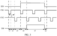
- FIG. 3 is a timing diagram of a driving method of the emission control circuit according to an embodiment of the present application.
- the timing diagram may be a timing diagram corresponding to a first stage of the emission control circuit in an emission control driver, and the timing diagram may be configured to drive the emission control circuit shown in FIG. 2 .
- EIN is an initial signal
- CK1 is a first clock signal
- CK2 is a second clock signal
- EM is an emission control signal.
- the first clock signal CK1 and the second clock signal CK2 have the same frequency
- the second clock signal CK2 has a delay time relative to the first clock signal CK1.
- the specific delay time is a T, and the T may be half of a period of the first clock signal CK1. Duration of the high level in the initial signal EIN may be twice the period of the first clock signal CK1.
- a duty period of the timing diagram shown in FIG. 3 may be divided into six phases: a first phase t1, a second phase t2, a third phase t3, a fourth phase t4, a fifth phase t5, and a sixth phase t6. Specifically:
- the initial signal EIN has a low level
- the first clock signal CK1 has a low level
- the second clock signal CK2 has a high level.
- the first thin film transistor M1 and the third thin film transistor M3 are in on-state, and the initial signal EIN is applied to the first node N1 through the first thin film transistor M1, so that the first node N1 has a low level, and then the second thin film transistor M2, the eighth thin film transistor M8, and the tenth thin film transistor M10 are in on-state.
- the first clock signal CK1 is applied to the second node N2 through the second thin film transistor M2, and the first power source VGL is applied to the second node N2 through the third thin film transistor M3, so that the second node N2 has a low level, and then the forth thin film transistors M4 and the sixth thin film transistor M6 are in on-state.
- the fifth thin film transistor M5 and the seventh thin film transistor M7 are in off-state. Since the eighth thin film transistor M8 is in on-state, the second power source VGH is applied to the third node N3 through the eighth thin film transistor M8, so that the third node N3 has a high level, and then the ninth thin film transistor M9 is in off-state.
- the first power source VGL may be output by the tenth thin film transistor M10, so that the emission control signal EM has a low level.
- the initial signal EIN has a low level
- the first clock signal CK1 has a high level
- the second clock signal CK2 has a high level.
- the first thin film transistor M1 and the third thin film transistor M3 are in off-state.
- the first node N1 since the second clock signal CK2 at another terminal of the third capacitor C3 remains unchanged, the first node N1 will has the low level of the first phase t1, and then the second thin film transistor M2, the eighth thin film transistor M8, and the tenth thin film transistor M10 are still in on-state.
- the first clock signal CK1 is applied to the second node N2 through the second thin film transistor M2, so that the second node N2 has the high level and the fourth thin film transistor M4 and the sixth thin film transistor M6 are in off-state.
- the fifth thin film transistor M5 and the seventh thin film transistor M7 are still in off-state. Since the eighth thin film transistor M8 is in on-state, the third node N3 has the high level due to the second power source VGH, and then the ninth thin film transistor M9 is still in off-state.
- the first power source VGL may be output by the tenth thin film transistor M10, so that the emission control signal EM has a low level.
- the initial signal EIN has a low level
- the first clock signal CK1 has a high level
- the second clock signal CK2 has a low level, and then changed from the low level to a high level.
- the first thin film transistor M1 and the third thin film transistor M3 are in off-state.
- the second clock signal CK2 has the low level
- the fifth thin film transistor M5 and the seventh thin film transistor M7 are in on-state, and because of a bootstrap effect of the third capacitor C3, the voltage of the first node N1 is lowered and the voltage of the first node N1 is lower than the voltage of the first node N1 in the second phase t2, and then the second thin film transistor M2, the eighth thin film transistor M8, and the tenth thin film transistor M10 are in on-state.
- the first clock signal CK1 is applied to the second node N2 through the second thin film transistor M2, so that the second node N2 still has the high level and then the fourth thin film transistor M4 and the sixth thin film transistor M6 are in off-state. Since the eighth thin film transistor M8 is in on-state, and the voltage of the second power source VGH is applied to the third node N3 through the eighth thin film transistor M8, so that the third node N3 still has the high level and then the ninth thin film transistor M9 is in off-state.
- the ninth thin film transistor M9 is in off-state and the tenth thin film transistor M10 is in on-state, the first power source VGL may be output by the tenth thin film transistor M10, so that the emission control signal EM has a low level.
- the fifth thin film transistor M5 and the seventh thin film transistor M7 are in off-state.
- the voltage of the first node N1 rises, but the first node N1 still has the low level, and then due to the first node N1, the second thin film transistor M2, the eighth thin film transistor M8, and the tenth thin film transistor M10 are still in on-state.
- the first thin film transistor M1 and the third thin film transistor M3 are still in off-state, and the first clock signal CK1 is applied to the second node N2 through the second thin film transistor M2, so that the second node N2 has the high level and then the fourth thin film transistor M4 and the sixth thin film transistor M6 are in off-state.
- the second power source VGH is applied to the third node N3 through the eighth thin film transistor M8, so that the third node N3 has the high level and then the ninth thin film transistor M9 is still in off-state.
- the ninth thin film transistor M9 is still in off-state and the tenth thin film transistor M10 is still in on-state, the first power source VGL may be output by the tenth thin film transistor M10, so that the emission control signal EM has a low level.
- the emission control signal EM has a low level.
- the initial signal EIN has a high level
- the first clock signal CK1 has a low level
- the second clock signal CK2 has a high level
- the first thin film transistor M1 and the third thin film transistor M3 are in on-state, and the initial signal EIN is applied to the first node N1 through the first thin film transistor M1, so that the first node N1 has the high level and then the second thin film transistor M2, the eighth thin film transistor M8, and the tenth thin film transistor M10 are in off-state.
- the first power source VGL is applied to the second node N2 through the third thin film transistor M3, so that the second node N2 has the low level, the fourth thin film transistor M4 and the sixth thin film transistor M6 are in on-state.
- the fifth thin film transistor M5 and the seventh thin film transistor M7 are in off-state. Since the eighth thin film transistor M8 is in off-state, under a storage control of the second capacitor C2, the third node N3 still has the high level being same as the high level in the third phase t3, and the ninth thin film transistor M9 turns to be in off-state.
- the emission control signal EM still has the low level being same as the low level in the third phase t3.
- the first clock signal CK1 has the high level
- the first thin film transistor M1 and the third thin film transistor M3 are in off-state
- the first node N1 will still has the high level
- the second node N2 will keep the low level unchanged
- the third node N3 will keep the high level unchanged.
- the second thin film transistor M2, the eighth thin film transistor M8, and the tenth thin film transistor M10 are still in off-state
- the fourth thin film transistor M4 and the sixth thin film transistor M6 are still in on-state
- the ninth thin film transistor M9 is still in off-state. Due to the second clock signal CK2, the fifth thin film transistor M5 and the seventh thin film transistor M7 are in off-state.
- the emission control signal EM keeps the low level being same as the low level in the third phase t3.
- the emission control signal EM has a low level.
- the initial signal EIN has a high level; the first clock signal CK1 has a high level, changed from the high level to a low level, and then changed from the low level to a high level; the second clock signal CK2 has a low level, changed from the low level to a high level, changed from the high level to a low level, and then changed from the low level to a high level.
- the first thin film transistor M1 and the third thin film transistor M3 are in off-state, and the fifth thin film transistor M5 and the seventh thin film transistor M7 are in on-state.
- the second node N2 is lowered and the voltage of the second node N2 is lower than the voltage of the second node N2 of the fourth stage t4, and then the fourth thin film transistor M4 and the sixth thin film transistor M6 are in on-state.
- the second clock signal CK2 may act on the third node N3 through the sixth thin film transistor M6 and the seventh thin film transistor M7, so that the third node N3 has the low level and then the ninth thin film transistor M9 is in on-state.
- the fourth thin film transistor M4 and the fifth thin film transistor M5 are on, the second power source VGH is applied to the first node N1 through the fourth thin film transistor M4 and the fifth thin film transistor M5, so that the first node N1 has the high level and then the second thin film transistor M2, the eighth thin film transistor M8, and the tenth thin film transistor M10 are in off-state.
- the second power source VGH may be output by the ninth thin film transistor M9, so that the emission control signal EM has a high level.
- the first node N1 still keeps the high level unchanged
- the voltage of the third node N3 still keeps the low level unchanged.
- the first clock signal CK1 is changed from the high level to the low level and the second clock signal CK2 still has the high level
- the first Node N1 still keeps the high level unchanged
- the third node N3 still keeps the low level unchanged.
- the first clock signal CK1 is changed from the low level to the high level
- the second clock signal CK2 is changed from the high level to the low level, and then changed from the low level to the high level
- the first node N1 still keeps the high level unchanged
- the third node N3 still keeps the low level unchanged.
- the ninth thin film transistor M9 is in on-state
- the tenth thin film transistor M10 is in off-state
- the second power source VGH may be output by the ninth thin film transistor M9, so that the emission control signal EM has a high level.
- the initial signal EIN has a low level
- the first clock signal CK1 has a low level
- the second clock signal CK2 has a high level.
- a working principle of the emission control circuit may be referred to a working principle of the emission control circuit in the first stage t1 described above, and a description of the working principle is not repeated herein.
- the emission control signal EM has a low level.
- a waveform diagram of the emission control signal EM which is output by the emission control unit may be as shown in FIG. 3 .
- the emission control circuit shown in FIG. 2 includes ten thin film transistors and three capacitors. Compared with the emission control circuit in the prior art, the number of thin film transistors and the number of capacitors are small, and the circuit structure of the emission control circuit is relatively simple.
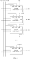
- FIG. 4 is a schematic structural diagram of an emission control driver according to an embodiment of the present application.
- the emission control driver may include at least two stages emission control circuit described in the first Embodiment.
- the emission control driver shown in FIG. 4 includes N stages of emission control circuits, which may include, respectively: an emission control circuit 1, an emission control circuit 2, an emission control circuit 3..., an emission control circuit n.
- the emission control circuit 1 is a first stage emission control circuit
- the emission control circuit 2 is a second stage emission control circuit
- the emission control circuit 3 is a third stage emission control circuit, ...
- the emission control circuit n is a nth stage emission control circuit, n is an integer greater than 1.
- an input signal of the emission control circuit 1 is an initial signal EIN
- an emission control signal EM1 output by the emission control circuit 1 may be used as an initial signal of the emission control circuit 2
- the emission control signal output by the emission control circuit 2 may be used as an initial signal of the emission control circuit 3
- the emission control signal EM(n-1) output by the emission control circuit (n-1) may be used as an initial signal of the emission control circuit n
- n is the integer greater than 1.
- a first clock signal of the emission control circuit 1 may be used as a second clock signal of the emission control circuit 2, and the second clock signal of the emission control circuit 1 may be used as a first clock signal of the emission control circuit 2; the first clock of the emission control circuit 2 may be used as a second clock signal of the emission control circuit 3, and the second clock signal of the emission control circuit 2 may be used as a first clock signal of the emission control circuit 3, ..., and so on, the first clock signal of the emission control circuit (n-1) may be used as a second clock signal of the emission control circuit n, and the second clock signal of the emission control circuit (n-1) may be used as a first clock signal of the emission control circuit n, and n is the integer greater than 1.
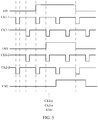
- FIG. 5 is a timing diagram of the emission control driver according to an embodiment of the present application.
- EIN is an initial signal input to a first stage of an emission control circuit
- CK1-1 is a first clock signal input to the emission control circuit 1
- CK2-1 is a second clock signal input to the emission control circuit 1
- the emission control circuit 1 may output an emission control signal EM1 under control of the initial signal EIN, the first clock signal CK1-1, and the second clock signal CK2-1.
- the emission control signal EM1 may be used as an initial signal of an emission control circuit 2.
- CK1-2 is a first clock signal input to the emission control circuit 2
- CK2-2 is a second clock signal input to the emission control circuit 2
- the emission control circuit 2 may output an emission control signal EM2 under control of the initial signal EIN, the first clock signal CK1-2, and the second clock signal CK2-2.
- the first clock signal CK1-2 of the emission control circuit 2 is the same as the second clock signal CK2-1 of the emission control circuit 1
- the second clock signal CK2-2 of the emission control circuit 2 is the same as the first clock signal CK1-1 of the emission control circuit 1
- the emission control signal EM2 output from the emission control circuit 2 is delayed with respect to the emission control signal EM1 output from the emission control circuit 1.
- an emission control signal EM(n-1) output by an emission control circuit (n-1) may be used as an initial signal of an emission control circuit n, and CK1-n is a first clock signal input to the emission control circuit n, CK2-n is a second clock signal input to the emission control circuit n.
- the first clock signal CK1-n may be the same as the second clock signal CK2-1, the second clock signal CK2-n may be the same as the first clock signal CK1-1, and the emission control circuit n may output the emission control signal EMn under control of the initial signal EM(n-1), the first clock signal CK1-n, and the second clock signal CK2-n.
- the initial signal EM(n-1), the first clock signal CK1-n, and the second clock signal CK2-n are not shown in FIG. 5 .
- the embodiments of the present application further provide a display device, which may include an emission control driver as described above.
Landscapes
- Engineering & Computer Science (AREA)
- Physics & Mathematics (AREA)
- Computer Hardware Design (AREA)
- General Physics & Mathematics (AREA)
- Theoretical Computer Science (AREA)
- Control Of Indicators Other Than Cathode Ray Tubes (AREA)
- Shift Register Type Memory (AREA)
- Electronic Switches (AREA)
- Control Of El Displays (AREA)
- Electroluminescent Light Sources (AREA)
Abstract
Description
- This application claims the priority of Chinese patent application No.
201820093773.2, filed on Jan. 19, 2018 - Embodiments of the present application relate to the field of display technologies, and more specifically to an emission control circuit, an emission control driver and a display device.
- Generally, a display device may include a plurality of pixels, a data driver, a scan driver, and an emission control driver. The plurality of pixels are configured to display an image, the data driver is configured to provide data voltages to the pixels, the scan driver is configured to provide scanning signals to the pixels, the emission control driver is configured to provide emission control signals to the pixels, and the emission control signals may control emission time of the pixels.
- As for an emission control driver, the emission control driver may include multiple-stages of emission control circuits, each of which may be configured to control emission time of a row of the pixels. As for one stage of emission control circuit, which may include a plurality of thin film transistors, an initial signal, and a plurality of clock signals, may control the thin film transistors to be in on-state or off-state, so that the emission control circuit can output the emission control signals.
- In the prior art, however, each stage of emission control circuit includes a large number of thin film transistors (usually more than 20), resulting in a complicated emission control circuit.
- In response to the above problems, an emission control circuit is provided in embodiments of the present application, and the circuit includes less thin film transistors and has a simple structure, to achieve requirements of simplifying a structure of the emitting control circuit.
- According to a first aspect of the present application, an emission control circuit is provided by the embodiments of the present application, and the emission control circuit includes a first control unit, a second control unit and an emission control unit.
- The first control unit configured to output a first control signal is respectively connected to an initial signal line, a first clock signal line and a first power source.
- The second control unit, an output terminal of which is respectively connected to a terminal of the first control unit, a second clock signal line and a second power source, is configured to output a second control signal.
- The emission control unit, an output terminal of which is respectively connected to the first control unit, the second control unit, the first power source and the second power source, is configured to output an emission control signal under control of the first control signal and the second control signal.
- In an embodiment, the emission control unit includes a ninth thin film transistor, a tenth thin film transistor, a second capacitor, and a third capacitor. A source of the ninth thin film transistor is connected to the second power source, a drain of the ninth thin film transistor is connected to a source of the tenth thin film transistor, and a gate of the ninth thin film transistor is connected to the output terminal, configured to output the second control signal, of the second control unit.
- A drain of the tenth thin film transistor is connected to the first power source, and a gate of the tenth thin film transistor is connected to the output terminal, configured to output the first control signal, of the first control unit.
- A terminal of the second capacitor is connected to an output terminal, configured to output the second control signal, of the second control unit, and another terminal of the second capacitor is connected to the second power source.
- And, a terminal of the third capacitor is connected to the second clock signal line, and another terminal of the third capacitor is connected to an output terminal, configured to output the first control signal, of the first control unit.
- The drain of the ninth thin film transistor or the source of the tenth thin film transistor is an output terminal of the emission control unit, and a signal output by the drain of the ninth thin film transistor or the source of the tenth thin film transistor is the emission control signal.
- In an embodiment, the tenth thin film transistor is controlled by the first control signal to be in on-state or off-state, and the ninth thin film transistor is controlled by the second control signal to be in on-state or off-state.
- In an embodiment, when the tenth thin film transistor is controlled by the first control signal to be in on-state, the ninth thin film transistor is controlled by the second control signal to be in off-state ; and,
when the tenth thin film transistor is controlled by the first control signal to be in off-state, the ninth thin film transistor is controlled by the second control signal to be in on-state. - In an embodiment, when the tenth thin film transistor is controlled by the first control signal to be in on-state, and the ninth thin film transistor is controlled by the second control signal to be in off-state, the emission control signal is a voltage output by the first power source.
- When the tenth thin film transistor is controlled by the first control signal to be in off-state, and the ninth thin film transistor is controlled by the second control signal to be in on-state, the emission control signal is a voltage output by the second power source.
- In an embodiment, the first control unit includes a first thin film transistor, a second thin film transistor, and a third thin film transistor.
- Wherein, a gate of the first thin film transistor is respectively connected to a source of the second thin film transistor, a gate of the third thin film transistor, and the first clock signal line, a drain of the first thin film transistor is connected to the initial signal line, and a source of the first thin film transistor is connected to a gate of the second thin film transistor; a drain of the second thin film transistor is connected to a source of the third thin film transistor; a drain of the third thin film transistor is connected to the first power source; and, the source of the first thin film transistor is the output terminal of the first control unit, and a signal output by the output terminal of the first control unit is the first control signal.
- In an embodiment, the second control unit includes a fourth thin film transistor, a fifth thin film transistor, a sixth thin film transistor, a seventh thin film transistor, an eighth thin film transistor, and a first capacitor; wherein,
a gate of the fourth thin film transistor is respectively connected to a gate of the sixth thin film transistor and a terminal of the first capacitor, a source of the fourth thin film transistor is connected to a source of the fifth thin film transistor, and a drain of the fourth thin film transistor is respectively connected to a drain of the eighth thin film transistor and the second power source;
a gate of the fifth thin film transistor is respectively connected to the second clock signal line, a drain of the sixth thin film transistor, a gate of the seventh thin film transistor, and another terminal of the first capacitor, and a drain of the fifth thin film transistor is respectively connected to a gate of the eighth thin film transistor and a source of the first thin film transistor;
a source of the sixth thin film transistor is connected to a source of the seventh thin film transistor, and a drain of the seventh thin film transistor is connected to a source of the eighth thin film transistor; and,
the source of the eighth thin film transistor is the output terminal of the second control unit, and a signal output by the output terminal of the second control unit is the second control signal. - In an embodiment, the initial signal line is configured to provide an initial signal, the first clock signal line is configured to provide a first clock signal, and the second clock signal line is configured to provide a second clock signal; and,
a voltage output by the first power source is a negative voltage, and a voltage output by the second power source is a positive voltage. - In an embodiment, the first thin film transistor, the second thin film transistor, the third thin film transistor, the fourth thin film transistor, the fifth thin film transistor, the sixth thin film transistor, the seventh thin film transistor, the eighth thin film transistor, the ninth thin film transistor, and the tenth thin film transistor are all P-type thin film transistors.
- In an embodiment, at least one thin film transistor of the first thin film transistor, the second thin film transistor, the third thin film transistor, the fourth thin film transistor, the fifth thin film transistor, the sixth thin film transistor, the seventh thin film transistor, the eighth thin film transistor, the ninth thin film transistor, and the tenth thin film transistor is an N-type thin film transistor.
- According to a second aspect of the present application, an emission control driver is also provided by the embodiments of the present application, and the emission control driver includes at least two stages of emission control circuits described above.
an signal input to a first stage emission control circuit is an initial signal, and an emission control signal output by a (n-1)th stage emission control circuit is used as an initial signal of a nth stage emission control circuit; and
a first clock signal input to the (n-1)th stage emission control circuit is used as a second clock signal input to the nth stage emission control circuit, and a second clock signal input to the (n-1)th stage emission control circuit is used as a first clock signal input to the nth stage emission control circuit, and n is an integer greater than 1. - According to a third aspect of the present application, a display device is also provided by the embodiments of the present application, and the display device includes the emission control driver described above.
- The beneficial effects achieved by at least one of the above-mentioned technical solutions adopted by the embodiments of the present application are as follows:
The emission control circuit according to the embodiments of the present application includes the first control unit, the second control unit, and the emission control unit. The input terminal of the first control unit configured to output the first control signal is respectively connected to the initial signal line, the first clock signal line and the first power source, and the input terminal of the second control unit configured to output the second control signal is respectively connected to the first control unit, the second clock signal line and the second power source; an input terminal of the emission control unit is respectively connected to the first control unit, the second control unit, the first power source and the second power source; an output of the emission control unit is configured to output an emission control signal under control of the first control signal and the second control signal. - The emission control signal output by the emission control circuit according to the embodiments of the present application may control pixels to emit light, and the circuit structure of the emission control circuit is relatively simple.
-
-
FIG. 1 is a schematic structural diagram of an emission control circuit according to an embodiment of the present application. -
FIG. 2 is a schematic structural diagram of another emission control circuit according to another embodiment of the present application. -
FIG. 3 is a timing diagram of a method for controlling emission according to an embodiment of the present application. -
FIG. 4 is a schematic structural diagram of an emission control driver according to an embodiment of the present application. -
FIG. 5 is a timing diagram of an emission control driver according to an embodiment of the present application. - In order to make the purposes, technical means and advantages of the present application clear, the present application will be further described in detail below with reference to the accompanying drawings. Obviously, the described embodiments are only a part of the embodiments of the present application, and not all of the embodiments of the present application. Based on the embodiments in the present application, all other embodiments, obtained by those skilled in the art without creative efforts, are within the scope of the present application.
- In the embodiments of the present application, a first thin film transistor, a second thin film transistor, a third thin film transistor, a fourth thin film transistor, a fifth thin film transistor, a sixth thin film transistor, a seventh thin film transistor, an eighth thin film transistor, a ninth thin film transistor, and a tenth thin film transistor may all be N-type thin film transistors, or all be P-type thin film transistors. Alternatively, at least one of the transistors may be N-type thin film transistors, and the rest of the transistors are P-type thin film transistors, which is not specifically limited herein.
- The technical solutions provided by the embodiments of the present application are described in detail below with reference to the accompanying drawings.
-
FIG. 1 is a schematic structural diagram of an emission control circuit according to an embodiment of the present application. The emission control circuit can generate an emission control signal that can control emission time of pixels. The emission control circuit is described below. - As shown in
FIG. 1 , the emission control circuit provided by the embodiments of the present application may include: afirst control unit 11, asecond control unit 12, and anemission control unit 13. - An input terminal of the
first control unit 11 may be respectively connected to an initial signal line, a first clock signal line, and a first power source VGL. The initial signal line may provide an initial signal EIN, the first clock signal line may provide a first clock signal CK1, the first clock signal CK1 may be a pulse signal, and the first power source VGL may has a negative voltage, i.e., the first power source VGL may output a low level. Thefirst control unit 11 may be configured to output a first control signal under control of the initial signal EIN, the first clock signal CK1, and the first power source VGL. - An input terminal of the
second control unit 12 may be respectively connected to thefirst control unit 11, a second clock signal line, and a second power source VGH. The second clock signal line may provide a second clock signal CK2, and the second clock signal CK2 may also be a pulse signal. The second power source VGH may have a positive voltage, i.e., the second power source VGH may output a high level. Thesecond control unit 12 may be configured to output a second control signal under control of thefirst control unit 11, the second clock signal CK2, and the second power source VGH. - An input terminal of the
emission control unit 13 may be respectively connected to thefirst control unit 11, thesecond control unit 12, the first power source VGL and the second power source VGH. The first control signal and the second control signal may be input to theemission control unit 13, and theemission control unit 13 may be configured to output an emission control signal EM under control of the first control signal and the second control signal. - A circuit structure of the emission control circuit provided by the embodiments of the present application is relatively simple. The emission control unit may output the emission control signal under control of the first control unit, the second control unit, the clock signal, and the voltage of the power source, and the emission control signal may control the emission time of the pixels.
- In an embodiment of the present application, the
emission control unit 13 may include: a ninth thin film transistor M9, a tenth thin film transistor M10, a second capacitor C2, and a third capacitor C3. A source of the ninth thin film transistor M9 is connected to the second power source VGH, a drain of the ninth thin film transistor M9 is connected to a source of the tenth thin film transistor M10, and a gate of the ninth thin film transistor M9 is connected to the output terminal, configured to output the second control signal, of thesecond control unit 12. - A drain of the tenth thin film transistor M10 is connected to the first power source VGL, and a gate of the tenth thin film transistor M10 is connected to the output terminal, configured to output the first control signal, of the
first control unit 11. - A terminal of the second capacitor C2 is connected to the output terminal, configured to output the second control signal, of the
second control unit 12, and another terminal of the second capacitor C2 is connected to the second power source VGH. - A terminal of the third capacitor C3 is connected to the second clock signal CK2, and another terminal of the third capacitor C3 is connected to the output terminal, configured to output the first control signal, of the
first control unit 11. - The drain of the ninth thin film transistor M9 or the source of the tenth thin film transistor M10 is the output terminal of the
emission control unit 13, and a signal output by the drain of the ninth thin film transistor M9 or the source of the tenth thin film transistor M10 is the emission control signal. - In another embodiment provided by the present application, the
first control unit 11 shown inFIG. 1 may include: a first thin film transistor, a second thin film transistor, and a third thin film transistor. - In another embodiment provided by the present application, the
second control unit 12 shown inFIG. 1 may include: a fourth thin film transistor, a fifth thin film transistor, a sixth thin film transistor, a seventh thin film transistor, an eighth thin film transistor, and a capacitor. - Referring to
FIG. 2, FIG. 2 is a schematic structural diagram of an emission control circuit according to another embodiment of the present application. Thefirst control unit 11 includes a first thin film transistor M1, a second thin film transistor M2, and a third thin film transistor M3.Thesecond control unit 12 includes a fourth thin film transistor M4, a fifth thin film transistor M5, a sixth thin film transistor M6, a seventh thin film transistor M7, an eighth thin film transistor M8, and a first capacitor C1. Theemission control unit 13 includes a ninth thin film transistor M9, a tenth thin film transistor M10, a second capacitor C2, and a third capacitor C3. The thin film transistors, shown inFIG. 2 , are all P-type thin film transistors. The circuit structure of the emission control circuit shown inFIG. 2 is as follows. - A gate of the first thin film transistor M1 is respectively connected to a source of the second thin film transistor M2, a gate of the third thin film transistor M3 and the first clock signal line, a drain of the first thin film transistor M1 is connected to the initial signal line, and a source of the first thin film transistor M1 is respectively connected to a gate of the second thin film transistor M2, a drain of the fifth thin film transistor M5, a gate of the eighth thin film transistor M8, a gate of the tenth thin film transistor M10 and one terminal of the third capacitor C3 (a first node N1 shown in
FIG. 2 ). - A drain of the second thin film transistor M2 is connected to a source of the third thin film transistor M3.
- A drain of the third thin film transistor M3 is connected to the first power source VGL.
- A gate of the fourth thin film transistor M4 is respectively connected to a gate of the sixth thin film transistor M6 and one terminal of the first capacitor C1 (a second node N2 shown in
FIG. 2 ), and a source of the fourth thin film transistor M4 is connected to a source of the fifth thin film M5, and a drain of the fourth thin film transistor M4 is respectively connected to a drain of the eighth thin film transistor M8 and the second power source VGH. - A gate of the fifth thin film transistor M5 is respectively connected to the second clock signal line, a drain of the sixth thin film transistor M6, a gate of the seventh thin film transistor M7, another terminal of the first capacitor C1, and another terminal of the third capacitor C3.
- A source of the sixth thin film transistor M6 is connected to a source of the seventh thin film transistor M7.
- A drain of the seventh thin film transistor M7 is respectively connected to a source of the eighth thin film transistor M8, a gate of the ninth thin film transistor M9, and a terminal of the second capacitor C2 (a third node N3 shown in
FIG. 2 ). - A source of the ninth thin film transistor M9 is respectively connected to the second power source VGH and another terminal of the second capacitor C2, and a drain of the ninth thin film transistor M9 is connected to a source of the tenth thin film transistor M10.
- A drain of the tenth thin film transistor M10 is connected to the first power source VGL.
- In the emission control circuit shown in
FIG. 2 , a signal output by the source of the first thin film transistor M1 (i.e., the first node N1 shown inFIG. 2 ) may be regarded as the first control signal; a signal output by the source of the eighth thin film transistor M8 (i.e., the third node N3 shown inFIG. 2 ) may be regarded as the second control signal; a signal output by the drain of the ninth thin film transistor M9 (or the source of the tenth thin film transistor M10) may be regarded as the emission control signal EM. - The first control signal may be output to the gate of the tenth thin film transistor M10 and the tenth thin film transistor M10 is controlled by the first control signal to be in on-state or off-state; the second control signal may be output to the gate of the ninth thin film transistor M9 and the ninth thin film transistor M9 is controlled by the second control signal to be in on-state or off-state. The emission control signal EM may be output to pixels and the emission control signal EM is configured to control emission time of the pixels.
- It should be understood that a type of the first thin film transistor M1, the second thin film transistor M2, the third thin film transistor M3, the fourth thin film transistor M4, the fifth thin film transistor M5, the sixth thin film transistor M6, the seventh thin film transistor M7, the eighth thin film transistor M8, the ninth thin film transistor M9 and the tenth thin film transistor M10, may be selected according to a practical application. For example, the first thin film transistor M1, the second thin film transistor M2, the third thin film transistor M3, the fourth thin film transistor M4, the fifth thin film transistor M5, the sixth thin film transistor M6, the seventh thin film transistor M7, the eighth thin film transistor M8, the ninth thin film transistor M9 and the tenth thin film transistor M10 may all be the P-type thin film transistor as described above, or at least one thin film transistor of the first thin film transistor M1, the second thin film transistor M2, the third thin film transistor M3, the fourth thin film transistor M4, the fifth thin film transistor M5, the sixth thin film transistor M6, the seventh thin film transistor M7, the eighth thin film transistor M8, the ninth thin film transistor M9 and the tenth thin film transistor M10 is the N-type thin film transistor.
- In an embodiment of the present application, the first capacitor C1 and the third capacitor C3 may be bootstrap capacitors configured to raise or lower a level of a node, and the second capacitor C2 may be a storage capacitor configured to maintain the level of the node. Specifically:
One terminal of the first capacitor C1 (i.e., the second node N2 shown inFIG. 2 ) is respectively connected to the gate of the fourth thin film transistor M4 and the gate of the sixth thin film transistor M6, and another terminal of the first capacitor C1 is connected to the second clock signal line. When a level of the second clock signal CK2 changes, the first capacitor C1 may be configured to raise or lower a level of the second node N2, and thereby the fourth thin film transistor M4 and the sixth thin film transistor M6 are controlled to be in on-state or off-state. - One terminal of the second capacitor C2 (i.e., the third node N3 shown in
FIG. 2 ) is respectively connected to the source of the eighth thin film transistor M8 and the gate of the ninth thin film transistor M9, and another terminal of the second capacitor C2 is connected to the second power source VGH. When the eighth thin film transistor M8 is in on-state, a voltage of the third node N3 is a high level, and when the eighth thin film transistor M8 is turned from being in on-state to being in off-state, since the second capacitor C2 is the storage capacitor, the second capacitor C2 may be configured to keep the high level of the third node N3 unchanged, and thereby the ninth thin film transistor M9 is controlled to remain being in off-state. - One terminal of the third capacitor C3 (i.e., the first node N1 shown in
FIG. 2 ) is respectively connected to the gate of the second thin film transistor M2, the gate of the eighth thin film transistor M8, and the gate of the tenth thin film transistor M10, and another terminal of the third capacitor C3 is connected to the second clock signal line. When the voltage output by the second clock signal CK2 changes, the third capacitor C3 may be configured to raise or pull down a voltage of the first node N1, and thereby the second thin film transistor M2, the eighth thin film transistor M8 and the tenth thin film transistor M10 are controlled to be in on-state or off-state. - It should be noted that, since another terminal of the first capacitor C1 is directly connected to the second clock signal line in the embodiment of the present application, a delay of the second clock signal CK2 to the first capacitor C1 can be reduced, and charging time of the second clock signal CK2 to the first capacitor C1 can be shortened, and thereby the control efficiency of the first capacitor C1 to the fourth thin film transistor M4 and the sixth thin film transistor M6 can be increased, so that the emission control circuit may work at a higher frequency and a higher frequency emission control signal EM is output. Similarly, for the third capacitor C3, another terminal of the third capacitor C3 is directly connected to the second clock signal line, and a delay of the second clock signal CK2 to the third capacitor C3 can be reduced, and the control efficiency of the third capacitor C3 to the second thin film transistor M2, the eighth thin film transistor M8, and the tenth thin film transistor M10 may be increased, so that a higher frequency emission control signal EM is output.
- In an embodiment of the present application, in order to ensure that the emission control circuit can output the emission control signal EM normally. In the embodiment of the present application, when the tenth thin film transistor M10 is controlled by the first control signal to be in on-state, the ninth thin film transistor M9 may be controlled by the second control signal to be in off-state; or, when the tenth thin film transistor M10 is controlled by the first control signal to be in off-state, the ninth thin film transistor M9 may be controlled by the second control signal to be in on-state.
- Specifically, as shown in
FIG. 2 , when the tenth thin film transistor M10 is controlled by the first control signal to be in on-state, and the ninth thin film transistor M9 is controlled by the second control signal to be in off-state, the first power source VGL may be output to an EM end for the emission control signal through the tenth thin film transistor M10, i.e., the emission control unit outputs the first power source VGL; when the tenth thin film transistor M10 is controlled by the first control signal to be in off-state, and the ninth thin film transistor M9 is controlled by the second control signal to be in on-state, the second power source VGH may be output to an EM end for the emission control signal through the ninth thin film transistor M9, i.e., the emission control unit outputs the second power source VGH. -
FIG. 3 is a timing diagram of a driving method of the emission control circuit according to an embodiment of the present application. The timing diagram may be a timing diagram corresponding to a first stage of the emission control circuit in an emission control driver, and the timing diagram may be configured to drive the emission control circuit shown inFIG. 2 . - In
FIG. 3 , EIN is an initial signal, CK1 is a first clock signal, CK2 is a second clock signal, and EM is an emission control signal. The first clock signal CK1 and the second clock signal CK2 have the same frequency, and the second clock signal CK2 has a delay time relative to the first clock signal CK1. The specific delay time is a T, and the T may be half of a period of the first clock signal CK1. Duration of the high level in the initial signal EIN may be twice the period of the first clock signal CK1. - A duty period of the timing diagram shown in
FIG. 3 may be divided into six phases: a first phase t1, a second phase t2, a third phase t3, a fourth phase t4, a fifth phase t5, and a sixth phase t6. Specifically: - The initial signal EIN has a low level, the first clock signal CK1 has a low level, and the second clock signal CK2 has a high level.
- Under control of the first clock signal CK1, the first thin film transistor M1 and the third thin film transistor M3 are in on-state, and the initial signal EIN is applied to the first node N1 through the first thin film transistor M1, so that the first node N1 has a low level, and then the second thin film transistor M2, the eighth thin film transistor M8, and the tenth thin film transistor M10 are in on-state. The first clock signal CK1 is applied to the second node N2 through the second thin film transistor M2, and the first power source VGL is applied to the second node N2 through the third thin film transistor M3, so that the second node N2 has a low level, and then the forth thin film transistors M4 and the sixth thin film transistor M6 are in on-state.
- Under control of the second clock signal CK2, the fifth thin film transistor M5 and the seventh thin film transistor M7 are in off-state. Since the eighth thin film transistor M8 is in on-state, the second power source VGH is applied to the third node N3 through the eighth thin film transistor M8, so that the third node N3 has a high level, and then the ninth thin film transistor M9 is in off-state.
- Thus, in the first phase t1, since the ninth thin film transistor M9 is in off-state and the tenth thin film transistor M10 is in on-state, the first power source VGL may be output by the tenth thin film transistor M10, so that the emission control signal EM has a low level.
- The initial signal EIN has a low level, the first clock signal CK1 has a high level, and the second clock signal CK2 has a high level.
- At this time, due to the first clock signal CK1, the first thin film transistor M1 and the third thin film transistor M3 are in off-state. For the first node N1, since the second clock signal CK2 at another terminal of the third capacitor C3 remains unchanged, the first node N1 will has the low level of the first phase t1, and then the second thin film transistor M2, the eighth thin film transistor M8, and the tenth thin film transistor M10 are still in on-state. The first clock signal CK1 is applied to the second node N2 through the second thin film transistor M2, so that the second node N2 has the high level and the fourth thin film transistor M4 and the sixth thin film transistor M6 are in off-state.
- Due to the second clock signal CK2, the fifth thin film transistor M5 and the seventh thin film transistor M7 are still in off-state. Since the eighth thin film transistor M8 is in on-state, the third node N3 has the high level due to the second power source VGH, and then the ninth thin film transistor M9 is still in off-state.
- Thus, in the second phase t2, since the ninth thin film transistor M9 is in off-state and the tenth thin film transistor M10 is in on-state, the first power source VGL may be output by the tenth thin film transistor M10, so that the emission control signal EM has a low level.
- The initial signal EIN has a low level, the first clock signal CK1 has a high level, the second clock signal CK2 has a low level, and then changed from the low level to a high level.
- At this time, due to the first clock signal CK1, the first thin film transistor M1 and the third thin film transistor M3 are in off-state. When the second clock signal CK2 has the low level, the fifth thin film transistor M5 and the seventh thin film transistor M7 are in on-state, and because of a bootstrap effect of the third capacitor C3, the voltage of the first node N1 is lowered and the voltage of the first node N1 is lower than the voltage of the first node N1 in the second phase t2, and then the second thin film transistor M2, the eighth thin film transistor M8, and the tenth thin film transistor M10 are in on-state. The first clock signal CK1 is applied to the second node N2 through the second thin film transistor M2, so that the second node N2 still has the high level and then the fourth thin film transistor M4 and the sixth thin film transistor M6 are in off-state. Since the eighth thin film transistor M8 is in on-state, and the voltage of the second power source VGH is applied to the third node N3 through the eighth thin film transistor M8, so that the third node N3 still has the high level and then the ninth thin film transistor M9 is in off-state.
- Thus, since the ninth thin film transistor M9 is in off-state and the tenth thin film transistor M10 is in on-state, the first power source VGL may be output by the tenth thin film transistor M10, so that the emission control signal EM has a low level.
- When the second clock signal CK2 is changed from the low level to the high level, the fifth thin film transistor M5 and the seventh thin film transistor M7 are in off-state. At this time, because of the bootstrap effect of the third capacitor C3, the voltage of the first node N1 rises, but the first node N1 still has the low level, and then due to the first node N1, the second thin film transistor M2, the eighth thin film transistor M8, and the tenth thin film transistor M10 are still in on-state. Due to the first clock signal CK1, the first thin film transistor M1 and the third thin film transistor M3 are still in off-state, and the first clock signal CK1 is applied to the second node N2 through the second thin film transistor M2, so that the second node N2 has the high level and then the fourth thin film transistor M4 and the sixth thin film transistor M6 are in off-state. The second power source VGH is applied to the third node N3 through the eighth thin film transistor M8, so that the third node N3 has the high level and then the ninth thin film transistor M9 is still in off-state.
- Thus, since the ninth thin film transistor M9 is still in off-state and the tenth thin film transistor M10 is still in on-state, the first power source VGL may be output by the tenth thin film transistor M10, so that the emission control signal EM has a low level.
- In summary, in the third phase t3, the emission control signal EM has a low level.
- The initial signal EIN has a high level, the first clock signal CK1 has a low level, and then changes from the low level to the high level, the second clock signal CK2 has a high level.
- At this time, when the first clock signal CK1 has the low level, the first thin film transistor M1 and the third thin film transistor M3 are in on-state, and the initial signal EIN is applied to the first node N1 through the first thin film transistor M1, so that the first node N1 has the high level and then the second thin film transistor M2, the eighth thin film transistor M8, and the tenth thin film transistor M10 are in off-state. The first power source VGL is applied to the second node N2 through the third thin film transistor M3, so that the second node N2 has the low level, the fourth thin film transistor M4 and the sixth thin film transistor M6 are in on-state.
- Due to the second clock signal CK2, the fifth thin film transistor M5 and the seventh thin film transistor M7 are in off-state. Since the eighth thin film transistor M8 is in off-state, under a storage control of the second capacitor C2, the third node N3 still has the high level being same as the high level in the third phase t3, and the ninth thin film transistor M9 turns to be in off-state.
- Thus, since the ninth thin film transistor M9 and the tenth thin film transistor M10 are both in off-state, the emission control signal EM still has the low level being same as the low level in the third phase t3.
- When the first clock signal CK1 has the high level, the first thin film transistor M1 and the third thin film transistor M3 are in off-state, the first node N1 will still has the high level, and the second node N2 will keep the low level unchanged, the third node N3 will keep the high level unchanged. At this time, the second thin film transistor M2, the eighth thin film transistor M8, and the tenth thin film transistor M10 are still in off-state, and the fourth thin film transistor M4 and the sixth thin film transistor M6 are still in on-state, and the ninth thin film transistor M9 is still in off-state. Due to the second clock signal CK2, the fifth thin film transistor M5 and the seventh thin film transistor M7 are in off-state.
- Thus, since the ninth thin film transistor M9 and the tenth thin film transistor M10 are both in off-state, the emission control signal EM keeps the low level being same as the low level in the third phase t3.
- In summary, in the fourth phase t4, the emission control signal EM has a low level.
- The initial signal EIN has a high level; the first clock signal CK1 has a high level, changed from the high level to a low level, and then changed from the low level to a high level; the second clock signal CK2 has a low level, changed from the low level to a high level, changed from the high level to a low level, and then changed from the low level to a high level.
- When the first clock signal CK1 has the high level and the second clock signal CK2 has the low level, the first thin film transistor M1 and the third thin film transistor M3 are in off-state, and the fifth thin film transistor M5 and the seventh thin film transistor M7 are in on-state. Under the bootstrap effect of the first capacitor C1, the second node N2 is lowered and the voltage of the second node N2 is lower than the voltage of the second node N2 of the fourth stage t4, and then the fourth thin film transistor M4 and the sixth thin film transistor M6 are in on-state. Since the sixth thin film transistor M6 and the seventh thin film transistor M7 are both in on-state, the second clock signal CK2 may act on the third node N3 through the sixth thin film transistor M6 and the seventh thin film transistor M7, so that the third node N3 has the low level and then the ninth thin film transistor M9 is in on-state. Meanwhile, since the fourth thin film transistor M4 and the fifth thin film transistor M5 are on, the second power source VGH is applied to the first node N1 through the fourth thin film transistor M4 and the fifth thin film transistor M5, so that the first node N1 has the high level and then the second thin film transistor M2, the eighth thin film transistor M8, and the tenth thin film transistor M10 are in off-state.
- Since the ninth thin film transistor M9 is in on-state and the tenth thin film transistor M10 is in off-state, the second power source VGH may be output by the ninth thin film transistor M9, so that the emission control signal EM has a high level.
- When the second clock signal CK2 is changed from the low level to the high level and the first clock signal CK1 still has the high level, according to the description of the fourth stage t4 described above, the first node N1 still keeps the high level unchanged, the voltage of the third node N3 still keeps the low level unchanged. When the first clock signal CK1 is changed from the high level to the low level and the second clock signal CK2 still has the high level, based on the description of the fourth stage t4 described above, the first Node N1 still keeps the high level unchanged, and the third node N3 still keeps the low level unchanged. Similarly, when the first clock signal CK1 is changed from the low level to the high level, the second clock signal CK2 is changed from the high level to the low level, and then changed from the low level to the high level, the first node N1 still keeps the high level unchanged, and the third node N3 still keeps the low level unchanged.
- In summary, in the fifth phase t5, when the first clock signal CK1 and the second clock signal CK2 are changed, the first node N1 will keep the high level unchanged, and the third node N3 will keep the low level unchanged. Therefore, the ninth thin film transistor M9 is in on-state, the tenth thin film transistor M10 is in off-state, the second power source VGH may be output by the ninth thin film transistor M9, so that the emission control signal EM has a high level.
- The initial signal EIN has a low level, the first clock signal CK1 has a low level, and the second clock signal CK2 has a high level.
- In the sixth stage t6, a working principle of the emission control circuit may be referred to a working principle of the emission control circuit in the first stage t1 described above, and a description of the working principle is not repeated herein.
- In the sixth stage t6, the emission control signal EM has a low level.
- In summary, in one duty period of the emission control circuit, a waveform diagram of the emission control signal EM which is output by the emission control unit may be as shown in
FIG. 3 . - The emission control circuit shown in
FIG. 2 includes ten thin film transistors and three capacitors. Compared with the emission control circuit in the prior art, the number of thin film transistors and the number of capacitors are small, and the circuit structure of the emission control circuit is relatively simple. -
FIG. 4 is a schematic structural diagram of an emission control driver according to an embodiment of the present application. The emission control driver may include at least two stages emission control circuit described in the first Embodiment. - The emission control driver shown in
FIG. 4 includes N stages of emission control circuits, which may include, respectively: anemission control circuit 1, anemission control circuit 2, anemission control circuit 3..., an emission control circuit n. Theemission control circuit 1 is a first stage emission control circuit, theemission control circuit 2 is a second stage emission control circuit, theemission control circuit 3 is a third stage emission control circuit, ..., and the emission control circuit n is a nth stage emission control circuit, n is an integer greater than 1. - In
FIG. 4 , an input signal of theemission control circuit 1 is an initial signal EIN, an emission control signal EM1 output by theemission control circuit 1 may be used as an initial signal of theemission control circuit 2, and the emission control signal output by theemission control circuit 2 may be used as an initial signal of theemission control circuit 3, ..., and so on, the emission control signal EM(n-1) output by the emission control circuit (n-1) may be used as an initial signal of the emission control circuit n, and n is the integer greater than 1. - A first clock signal of the
emission control circuit 1 may be used as a second clock signal of theemission control circuit 2, and the second clock signal of theemission control circuit 1 may be used as a first clock signal of theemission control circuit 2; the first clock of theemission control circuit 2 may be used as a second clock signal of theemission control circuit 3, and the second clock signal of theemission control circuit 2 may be used as a first clock signal of theemission control circuit 3, ..., and so on, the first clock signal of the emission control circuit (n-1) may be used as a second clock signal of the emission control circuit n, and the second clock signal of the emission control circuit (n-1) may be used as a first clock signal of the emission control circuit n, and n is the integer greater than 1. -
FIG. 5 is a timing diagram of the emission control driver according to an embodiment of the present application. - In
FIG. 5 , EIN is an initial signal input to a first stage of an emission control circuit, CK1-1 is a first clock signal input to theemission control circuit 1, and CK2-1 is a second clock signal input to theemission control circuit 1, and theemission control circuit 1 may output an emission control signal EM1 under control of the initial signal EIN, the first clock signal CK1-1, and the second clock signal CK2-1. The emission control signal EM1 may be used as an initial signal of anemission control circuit 2. - CK1-2 is a first clock signal input to the
emission control circuit 2, CK2-2 is a second clock signal input to theemission control circuit 2, and theemission control circuit 2 may output an emission control signal EM2 under control of the initial signal EIN, the first clock signal CK1-2, and the second clock signal CK2-2. It can be seen fromFIG. 5 that the first clock signal CK1-2 of theemission control circuit 2 is the same as the second clock signal CK2-1 of theemission control circuit 1, and the second clock signal CK2-2 of theemission control circuit 2 is the same as the first clock signal CK1-1 of theemission control circuit 1, and the emission control signal EM2 output from theemission control circuit 2 is delayed with respect to the emission control signal EM1 output from theemission control circuit 1. - As an analogy, an emission control signal EM(n-1) output by an emission control circuit (n-1) may be used as an initial signal of an emission control circuit n, and CK1-n is a first clock signal input to the emission control circuit n, CK2-n is a second clock signal input to the emission control circuit n. The first clock signal CK1-n may be the same as the second clock signal CK2-1, the second clock signal CK2-n may be the same as the first clock signal CK1-1, and the emission control circuit n may output the emission control signal EMn under control of the initial signal EM(n-1), the first clock signal CK1-n, and the second clock signal CK2-n. The initial signal EM(n-1), the first clock signal CK1-n, and the second clock signal CK2-n are not shown in
FIG. 5 . - The embodiments of the present application further provide a display device, which may include an emission control driver as described above.
- It should be understood by those skilled in the art that, although preferred embodiments of the present application have been described, once basic creative concepts are known to those skilled in the art, additional changes and modifications may be made to these embodiments. Therefore, the appended claims are intended to be interpreted as including the preferred embodiments and all changes and modifications that fall within the scope of the present application.
- Obviously, those skilled in the art may make various changes and modifications to the present application without departing from the spirit and scope of the present application. In this way, if such modifications and variations of the present application are within the scope of the claims of the present application and its equivalent technologies, the present application is also intended to include such modifications and variations.
Claims (12)
- An emission control circuit, characterized in comprising: a first control unit (11), a second control unit (12), and an emission control unit (13), wherein:the first control unit (11), of which an output terminal is configured to output a first control signal, is connected to an initial signal line (EIN), a first clock signal line (CK1) and a first power source (VGL) respectively;the second control unit (12), of which an output terminal is configured to output a second control signal, is connected to the first control unit (11), a second clock signal line (CK1) and a second power source (VGH) respectively; andthe emission control unit (13), of which an output terminal of is configured to output an emission control signal under control of the first control signal and the second control signal, is connected to the first control unit (11), the second control unit (12), the first power source (VGL) and the second power source (VGH) respectively.
- The emission control circuit of claim 1, wherein the emission control unit (13) comprises a ninth thin film transistor (M9), a tenth thin film transistor (M10), a second capacitor (C2), and a third capacitor (C3), wherein:a source of the ninth thin film transistor (M9) is connected to the second power source (C2), a drain of the ninth thin film transistor (M9) is connected to a source of the tenth thin film transistor (M10), and a gate of the ninth thin film transistor (M9) is connected to an output terminal, configured to output the second control signal, of the second control unit (12);a drain of the tenth thin film transistor (M10) is connected to the first power source (VGL), and a gate of the tenth thin film transistor (M10) is connected to an output terminal, configured to output the first control signal, of the first control unit (11);a terminal of the second capacitor (C2) is connected to the output terminal of the second control unit (12) configured to output the second control signal, and another terminal of the second capacitor (C2) is connected to the second power source (VGH);a terminal of the third capacitor (C3) is connected to the second clock signal (CK2), and another terminal of the third capacitor (C3) is connected to the output terminal, configured to output the first control signal, of the first control unit (11),wherein the drain of the ninth thin film transistor (M9) or the source of the tenth thin film transistor (M10) is an output terminal of the emission control unit (13), and a signal output by the drain of the ninth thin film transistor (M9) or the source of the tenth thin film transistor (M10) is the emission control signal.
- The emission control circuit of claim 2, wherein the tenth thin film transistor (M10) is controlled by the first control signal to be in on-state or off-state, and the ninth thin film transistor (M9) is controlled by the second control signal to be in on-state or off-state.
- The emission control circuit of claim 3, wherein
the ninth thin film transistor (M9) is controlled by the second control signal to be in off-state when the tenth thin film transistor (M10) is controlled by the first control signal to be in on-state; and
the ninth thin film transistor (M9) is controlled by the second control signal to be in on-state when the tenth thin film transistor (M10) to be in off-state is controlled by the first control signal. - The emission control circuit of claim 4, wherein
when the tenth thin film transistor (M9) is controlled by the first control signal to be in on-state and the ninth thin film transistor (M10) is controlled by the second control signal to be in off-state, the emission control signal is a voltage output by the first power source; and
when the tenth thin film transistor (M9) is controlled by the first control signal to be in off-state, and the ninth thin film transistor (M10) is controlled by the second control signal to be in on-state, the emission control signal is a voltage output by the second power source. - The emission control circuit of any one of claims 1 to 5, wherein the first control unit (11) comprises a first thin film transistor (M1), a second thin film transistor (M2), and a third thin film transistor (M3), wherein
a gate of the first thin film transistor (M1) is respectively connected to a source of the second thin film transistor (M2), a gate of the third thin film transistor (M3) and the first clock signal line (CK1); a drain of the first thin film transistor (M1) is connected to the initial signal line (EIN), and a source of the first thin film transistor (M1) is connected to a gate of the second thin film transistor (M2);
a drain of the second thin film transistor (M2) is connected to a source of the third thin film transistor (M3);
a drain of the third thin film transistor (M3) is connected to the first power source (VGL); and,
the source of the first thin film transistor (M1) is the output terminal of the first control unit (11), and a signal output by the output terminal of the first control unit (11) is the first control signal. - The emission control circuit of claim 6, wherein the second control unit (12) comprises a fourth thin film transistor (M4), a fifth thin film transistor (M5), a sixth thin film transistor (M6), a seventh thin film transistor (M7), an eighth thin film transistor (M8), and a first capacitor (C1), wherein
a gate of the fourth thin film transistor (M4) is respectively connected to a gate of the sixth thin film transistor (M6) and a terminal of the first capacitor (C1), a source of the fourth thin film transistor (M4) is connected to a source of the fifth thin film transistor (M5), and a drain of the fourth thin film transistor (M4) is respectively connected to a drain of the eighth thin film transistor (M8) and the second power source (VGH);
a gate of the fifth thin film transistor (M5) is respectively connected to the second clock signal line (CK2), a drain of the sixth thin film transistor (M6), a gate of the seventh thin film transistor (M7) and another terminal of the first capacitor (C1), and a drain of the fifth thin film transistor (M5) is respectively connected to a gate of the eighth thin film transistor (M8) and a source of the first thin film transistor (M1);
a source of the sixth thin film transistor (M6) is connected to a source of the seventh thin film transistor (M7), and a drain of the seventh thin film transistor (M7) is connected to a source of the eighth thin film transistor (M8); and
the source of the eighth thin film transistor (M8) is the output terminal of the second control unit (12), and a signal output by the output terminal of the second control unit (12) is the second control signal. - The emission control circuit of claim 1, wherein
the initial signal line (EIN) is configured to provide an initial signal, the first clock signal line (CK1) is configured to provide a first clock signal, and the second clock signal line (CK2) is configured to provide a second clock signal;
a voltage output by the first power source (VGL) is a negative voltage, and a voltage output by the second power source (VGH) is a positive voltage. - The emission control circuit of claim 7, wherein the first thin film transistor (M1), the second thin film transistor (M2), the third thin film transistor (M3), the fourth thin film transistor (M4), the fifth thin film transistor (M5), the sixth thin film transistor (M6), the seventh thin film transistor (M7), the eighth thin film transistor (M8), the ninth thin film transistor (M9) and the tenth thin film transistor (M10) are all P-type thin film transistors.
- The emission control circuit of claim 7, wherein at least one of the first thin film transistor (M1), the second thin film transistor (M2), the third thin film transistor (M3), the fourth thin film transistor (M4), the fifth thin film transistor (M5), the sixth thin film transistor (M6), the seventh thin film transistor (M7), the eighth thin film transistor (M8), the ninth thin film transistor (M9), and the tenth thin film transistor (M10) is an N-type thin film transistor.
- An emission control driver, characterized in comprising at least two stages of emission control circuits according to any one of claims 1 to 10, wherein,
a signal input to a first stage emission control circuit is an initial signal, and an emission control signal output by a (n-1)th stage emission control circuit is used as an initial signal of a nth stage emission control circuit; and
a first clock signal input to the (n-1)th stage emission control circuit is used as a second clock signal input to the nth stage emission control circuit, and a second clock signal input to the (n-1)th stage emission control circuit is used as a first clock signal input to the nth stage emission control circuit, and n is an integer greater than 1. - A display device, characterized in comprising the emission control driver according to claim 11.
Applications Claiming Priority (2)
| Application Number | Priority Date | Filing Date | Title |
|---|---|---|---|
| CN201820093773.2U CN207781162U (en) | 2018-01-19 | 2018-01-19 | A kind of emission control circuit, light emitting control driver and display device |
| PCT/CN2018/107595 WO2019140946A1 (en) | 2018-01-19 | 2018-09-26 | Light emitting control circuit, light emitting control driver and display device |
Publications (3)
| Publication Number | Publication Date |
|---|---|
| EP3624100A1 true EP3624100A1 (en) | 2020-03-18 |
| EP3624100A4 EP3624100A4 (en) | 2020-07-01 |
| EP3624100B1 EP3624100B1 (en) | 2021-06-02 |
Family
ID=63213619
Family Applications (1)
| Application Number | Title | Priority Date | Filing Date |
|---|---|---|---|
| EP18901277.6A Active EP3624100B1 (en) | 2018-01-19 | 2018-09-26 | Light emitting control circuit, light emitting control driver and display device |
Country Status (7)
| Country | Link |
|---|---|
| US (1) | US20190213939A1 (en) |
| EP (1) | EP3624100B1 (en) |
| JP (1) | JP6829329B2 (en) |
| KR (1) | KR102271633B1 (en) |
| CN (1) | CN207781162U (en) |
| TW (1) | TWM574320U (en) |
| WO (1) | WO2019140946A1 (en) |
Families Citing this family (5)
| Publication number | Priority date | Publication date | Assignee | Title |
|---|---|---|---|---|
| CN207781162U (en) * | 2018-01-19 | 2018-08-28 | 昆山国显光电有限公司 | A kind of emission control circuit, light emitting control driver and display device |
| US11900881B2 (en) * | 2020-06-04 | 2024-02-13 | Chengdu Boe Optoelectronics Technology Co., Ltd. | Display substrate, manufacturing method thereof, and display device |
| US12293725B2 (en) | 2020-06-04 | 2025-05-06 | Chengdu Boe Optoelectronics Technology Co., Ltd. | Display substrate, manufacturing method thereof, and display device |
| KR20230064697A (en) | 2021-11-03 | 2023-05-11 | 삼성디스플레이 주식회사 | Light emission control driver |
| KR20230146171A (en) | 2022-04-11 | 2023-10-19 | 삼성디스플레이 주식회사 | Gate driver |
Family Cites Families (16)
| Publication number | Priority date | Publication date | Assignee | Title |
|---|---|---|---|---|
| JP4993544B2 (en) * | 2005-03-30 | 2012-08-08 | 三菱電機株式会社 | Shift register circuit |
| KR100873072B1 (en) * | 2006-08-31 | 2008-12-09 | 삼성모바일디스플레이주식회사 | Light emission control driver and organic light emitting display device using the same |
| JP2008216961A (en) * | 2007-03-02 | 2008-09-18 | Samsung Sdi Co Ltd | Organic light emitting display and driving circuit thereof |
| JP5063706B2 (en) * | 2007-12-27 | 2012-10-31 | シャープ株式会社 | Shift register and display device |
| CN102708795B (en) * | 2012-02-29 | 2014-11-12 | 京东方科技集团股份有限公司 | Gate driver on array unit, gate driver on array circuit and display device |
| KR20130135506A (en) * | 2012-06-01 | 2013-12-11 | 삼성디스플레이 주식회사 | Pixel and organic light emitting display device using the same |
| KR101975581B1 (en) * | 2012-08-21 | 2019-09-11 | 삼성디스플레이 주식회사 | Emission driver and organic light emitting display deivce including the same |
| KR101962432B1 (en) * | 2012-09-20 | 2019-03-27 | 삼성디스플레이 주식회사 | Stage Circuit and Organic Light Emitting Display Device Using the same |
| CN103198781B (en) * | 2013-03-01 | 2015-04-29 | 合肥京东方光电科技有限公司 | Shifting register unit and gate driving device and display device |
| CN104751770B (en) * | 2013-12-25 | 2018-01-16 | 昆山国显光电有限公司 | Emission control drive circuit and the OLED using the circuit |
| KR102460685B1 (en) * | 2016-01-18 | 2022-11-01 | 삼성디스플레이 주식회사 | Organic light emittng display device and driving method thereof |
| KR102477486B1 (en) * | 2016-04-19 | 2022-12-14 | 삼성디스플레이 주식회사 | Emission control driver and display device having the same |
| CN107039014B (en) * | 2017-05-26 | 2019-03-05 | 京东方科技集团股份有限公司 | Shift register unit, driving method thereof, gate driving circuit and display panel |
| CN108230998B (en) * | 2018-01-19 | 2020-01-24 | 昆山国显光电有限公司 | Emission control drive circuit, emission control driver, and organic light emitting display device |
| CN207781162U (en) * | 2018-01-19 | 2018-08-28 | 昆山国显光电有限公司 | A kind of emission control circuit, light emitting control driver and display device |
| CN108447439B (en) * | 2018-05-14 | 2019-07-02 | 昆山国显光电有限公司 | Array substrate, display screen and display device |
-
2018
- 2018-01-19 CN CN201820093773.2U patent/CN207781162U/en active Active
- 2018-09-26 WO PCT/CN2018/107595 patent/WO2019140946A1/en not_active Ceased
- 2018-09-26 EP EP18901277.6A patent/EP3624100B1/en active Active
- 2018-09-26 JP JP2019569419A patent/JP6829329B2/en active Active
- 2018-09-26 KR KR1020197035935A patent/KR102271633B1/en active Active
- 2018-10-05 TW TW107213522U patent/TWM574320U/en unknown
-
2019
- 2019-03-15 US US16/355,282 patent/US20190213939A1/en not_active Abandoned
Also Published As
| Publication number | Publication date |
|---|---|
| JP2020524357A (en) | 2020-08-13 |
| KR102271633B1 (en) | 2021-07-02 |
| CN207781162U (en) | 2018-08-28 |
| WO2019140946A1 (en) | 2019-07-25 |
| EP3624100A4 (en) | 2020-07-01 |
| EP3624100B1 (en) | 2021-06-02 |
| US20190213939A1 (en) | 2019-07-11 |
| TWM574320U (en) | 2019-02-11 |
| JP6829329B2 (en) | 2021-02-10 |
| KR20190141781A (en) | 2019-12-24 |
Similar Documents
| Publication | Publication Date | Title |
|---|---|---|
| US11158226B2 (en) | Gate driving unit and method, gate driving module and circuit and display device | |
| US11763740B2 (en) | Signal generation circuit, signal generation method, signal generation module and display device | |
| US11081061B2 (en) | Shift register, gate driving circuit, display device and gate driving method | |
| US11263951B2 (en) | Shift register unit and driving method thereof, gate driving circuit, and display device | |
| US10789868B2 (en) | Shift register circuit and method for driving the same, gate driving circuit and method for driving the same, and display apparatus | |
| US12198629B2 (en) | Pixel circuit for threshold compensation, driving method thereof and display device for providing signals | |
| US9865211B2 (en) | Shift register unit, gate driving circuit and display device | |
| EP3624100B1 (en) | Light emitting control circuit, light emitting control driver and display device | |
| CN215895935U (en) | Scanning circuit and display panel | |
| US20200266809A1 (en) | Shift Register and Driving Method Thereof, Cascade Driving Circuit and Display Device | |
| CN103198866B (en) | Shift register, gate driver circuit, array base palte and display device | |
| US11069274B2 (en) | Shift register unit, gate driving circuit, driving method and display apparatus | |
| US20210366353A1 (en) | Shift register unit and method for driving the same, gate driving circuit and display device | |
| CN112820234B (en) | Shift register circuit and display device | |
| CN112102768B (en) | GOA circuit and display panel | |
| US10134338B2 (en) | Inverter, gate driving circuit and display apparatus | |
| CN110070828B (en) | GOA circuit and display panel | |
| CN112927645A (en) | Driving circuit, driving method and display device | |
| KR20180118222A (en) | Shift register circuit, GOA circuit, and display device and driving method thereof | |
| CN110349536B (en) | GOA circuit and display panel | |
| CN110085160B (en) | GOA circuit and display panel | |
| CN114333673A (en) | Gate drive unit, gate drive circuit and display device | |
| CN110322843B (en) | GOA unit, GOA circuit and display panel | |
| CN119132235B (en) | Transmitting pulse generating circuit and transmitting pulse generating method | |
| CN111261108A (en) | Gate drive circuit |
Legal Events
| Date | Code | Title | Description |
|---|---|---|---|
| STAA | Information on the status of an ep patent application or granted ep patent |
Free format text: STATUS: THE INTERNATIONAL PUBLICATION HAS BEEN MADE |
|
| PUAI | Public reference made under article 153(3) epc to a published international application that has entered the european phase |
Free format text: ORIGINAL CODE: 0009012 |
|
| STAA | Information on the status of an ep patent application or granted ep patent |
Free format text: STATUS: REQUEST FOR EXAMINATION WAS MADE |
|
| 17P | Request for examination filed |
Effective date: 20191212 |
|
| AK | Designated contracting states |
Kind code of ref document: A1 Designated state(s): AL AT BE BG CH CY CZ DE DK EE ES FI FR GB GR HR HU IE IS IT LI LT LU LV MC MK MT NL NO PL PT RO RS SE SI SK SM TR |
|
| AX | Request for extension of the european patent |
Extension state: BA ME |
|
| A4 | Supplementary search report drawn up and despatched |
Effective date: 20200529 |
|
| RIC1 | Information provided on ipc code assigned before grant |
Ipc: G11C 19/28 20060101ALI20200525BHEP Ipc: G09G 3/32 20160101AFI20200525BHEP Ipc: G09G 3/3266 20160101ALI20200525BHEP |
|
| RAP1 | Party data changed (applicant data changed or rights of an application transferred) |
Owner name: KUNSHAN GO-VISIONOX OPTO-ELECTRONICS CO., LTD. |
|
| RAP1 | Party data changed (applicant data changed or rights of an application transferred) |
Owner name: KUNSHAN GO-VISIONOX OPTO-ELECTRONICS CO., LTD. |
|
| GRAP | Despatch of communication of intention to grant a patent |
Free format text: ORIGINAL CODE: EPIDOSNIGR1 |
|
| STAA | Information on the status of an ep patent application or granted ep patent |
Free format text: STATUS: GRANT OF PATENT IS INTENDED |
|
| GRAS | Grant fee paid |
Free format text: ORIGINAL CODE: EPIDOSNIGR3 |
|
| DAV | Request for validation of the european patent (deleted) | ||
| DAX | Request for extension of the european patent (deleted) | ||
| INTG | Intention to grant announced |
Effective date: 20210329 |
|
| RIN1 | Information on inventor provided before grant (corrected) |
Inventor name: WU, JIANLONG Inventor name: HU, SIMING Inventor name: ZHU, HUI |
|
| GRAA | (expected) grant |
Free format text: ORIGINAL CODE: 0009210 |
|
| STAA | Information on the status of an ep patent application or granted ep patent |
Free format text: STATUS: THE PATENT HAS BEEN GRANTED |
|
| REG | Reference to a national code |
Ref country code: CH Ref legal event code: EP |
|
| AK | Designated contracting states |
Kind code of ref document: B1 Designated state(s): AL AT BE BG CH CY CZ DE DK EE ES FI FR GB GR HR HU IE IS IT LI LT LU LV MC MK MT NL NO PL PT RO RS SE SI SK SM TR |
|
| REG | Reference to a national code |
Ref country code: GB Ref legal event code: FG4D |
|
| REG | Reference to a national code |
Ref country code: AT Ref legal event code: REF Ref document number: 1399176 Country of ref document: AT Kind code of ref document: T Effective date: 20210615 |
|
| REG | Reference to a national code |
Ref country code: IE Ref legal event code: FG4D |
|
| REG | Reference to a national code |
Ref country code: DE Ref legal event code: R096 Ref document number: 602018018202 Country of ref document: DE |
|
| REG | Reference to a national code |
Ref country code: LT Ref legal event code: MG9D |
|
| PG25 | Lapsed in a contracting state [announced via postgrant information from national office to epo] |
Ref country code: BG Free format text: LAPSE BECAUSE OF FAILURE TO SUBMIT A TRANSLATION OF THE DESCRIPTION OR TO PAY THE FEE WITHIN THE PRESCRIBED TIME-LIMIT Effective date: 20210902 Ref country code: FI Free format text: LAPSE BECAUSE OF FAILURE TO SUBMIT A TRANSLATION OF THE DESCRIPTION OR TO PAY THE FEE WITHIN THE PRESCRIBED TIME-LIMIT Effective date: 20210602 Ref country code: HR Free format text: LAPSE BECAUSE OF FAILURE TO SUBMIT A TRANSLATION OF THE DESCRIPTION OR TO PAY THE FEE WITHIN THE PRESCRIBED TIME-LIMIT Effective date: 20210602 Ref country code: LT Free format text: LAPSE BECAUSE OF FAILURE TO SUBMIT A TRANSLATION OF THE DESCRIPTION OR TO PAY THE FEE WITHIN THE PRESCRIBED TIME-LIMIT Effective date: 20210602 |
|
| REG | Reference to a national code |
Ref country code: NL Ref legal event code: MP Effective date: 20210602 |
|
| REG | Reference to a national code |
Ref country code: AT Ref legal event code: MK05 Ref document number: 1399176 Country of ref document: AT Kind code of ref document: T Effective date: 20210602 |
|
| PG25 | Lapsed in a contracting state [announced via postgrant information from national office to epo] |
Ref country code: GR Free format text: LAPSE BECAUSE OF FAILURE TO SUBMIT A TRANSLATION OF THE DESCRIPTION OR TO PAY THE FEE WITHIN THE PRESCRIBED TIME-LIMIT Effective date: 20210903 Ref country code: RS Free format text: LAPSE BECAUSE OF FAILURE TO SUBMIT A TRANSLATION OF THE DESCRIPTION OR TO PAY THE FEE WITHIN THE PRESCRIBED TIME-LIMIT Effective date: 20210602 Ref country code: SE Free format text: LAPSE BECAUSE OF FAILURE TO SUBMIT A TRANSLATION OF THE DESCRIPTION OR TO PAY THE FEE WITHIN THE PRESCRIBED TIME-LIMIT Effective date: 20210602 Ref country code: LV Free format text: LAPSE BECAUSE OF FAILURE TO SUBMIT A TRANSLATION OF THE DESCRIPTION OR TO PAY THE FEE WITHIN THE PRESCRIBED TIME-LIMIT Effective date: 20210602 Ref country code: NO Free format text: LAPSE BECAUSE OF FAILURE TO SUBMIT A TRANSLATION OF THE DESCRIPTION OR TO PAY THE FEE WITHIN THE PRESCRIBED TIME-LIMIT Effective date: 20210902 Ref country code: PL Free format text: LAPSE BECAUSE OF FAILURE TO SUBMIT A TRANSLATION OF THE DESCRIPTION OR TO PAY THE FEE WITHIN THE PRESCRIBED TIME-LIMIT Effective date: 20210602 |
|
| PG25 | Lapsed in a contracting state [announced via postgrant information from national office to epo] |
Ref country code: SK Free format text: LAPSE BECAUSE OF FAILURE TO SUBMIT A TRANSLATION OF THE DESCRIPTION OR TO PAY THE FEE WITHIN THE PRESCRIBED TIME-LIMIT Effective date: 20210602 Ref country code: ES Free format text: LAPSE BECAUSE OF FAILURE TO SUBMIT A TRANSLATION OF THE DESCRIPTION OR TO PAY THE FEE WITHIN THE PRESCRIBED TIME-LIMIT Effective date: 20210602 Ref country code: EE Free format text: LAPSE BECAUSE OF FAILURE TO SUBMIT A TRANSLATION OF THE DESCRIPTION OR TO PAY THE FEE WITHIN THE PRESCRIBED TIME-LIMIT Effective date: 20210602 Ref country code: CZ Free format text: LAPSE BECAUSE OF FAILURE TO SUBMIT A TRANSLATION OF THE DESCRIPTION OR TO PAY THE FEE WITHIN THE PRESCRIBED TIME-LIMIT Effective date: 20210602 Ref country code: AT Free format text: LAPSE BECAUSE OF FAILURE TO SUBMIT A TRANSLATION OF THE DESCRIPTION OR TO PAY THE FEE WITHIN THE PRESCRIBED TIME-LIMIT Effective date: 20210602 Ref country code: RO Free format text: LAPSE BECAUSE OF FAILURE TO SUBMIT A TRANSLATION OF THE DESCRIPTION OR TO PAY THE FEE WITHIN THE PRESCRIBED TIME-LIMIT Effective date: 20210602 Ref country code: PT Free format text: LAPSE BECAUSE OF FAILURE TO SUBMIT A TRANSLATION OF THE DESCRIPTION OR TO PAY THE FEE WITHIN THE PRESCRIBED TIME-LIMIT Effective date: 20211004 Ref country code: NL Free format text: LAPSE BECAUSE OF FAILURE TO SUBMIT A TRANSLATION OF THE DESCRIPTION OR TO PAY THE FEE WITHIN THE PRESCRIBED TIME-LIMIT Effective date: 20210602 Ref country code: SM Free format text: LAPSE BECAUSE OF FAILURE TO SUBMIT A TRANSLATION OF THE DESCRIPTION OR TO PAY THE FEE WITHIN THE PRESCRIBED TIME-LIMIT Effective date: 20210602 |
|
| REG | Reference to a national code |
Ref country code: DE Ref legal event code: R097 Ref document number: 602018018202 Country of ref document: DE |
|
| PLBE | No opposition filed within time limit |
Free format text: ORIGINAL CODE: 0009261 |
|
| STAA | Information on the status of an ep patent application or granted ep patent |
Free format text: STATUS: NO OPPOSITION FILED WITHIN TIME LIMIT |
|
| PG25 | Lapsed in a contracting state [announced via postgrant information from national office to epo] |
Ref country code: DK Free format text: LAPSE BECAUSE OF FAILURE TO SUBMIT A TRANSLATION OF THE DESCRIPTION OR TO PAY THE FEE WITHIN THE PRESCRIBED TIME-LIMIT Effective date: 20210602 |
|
| 26N | No opposition filed |
Effective date: 20220303 |
|
| REG | Reference to a national code |
Ref country code: CH Ref legal event code: PL |
|
| REG | Reference to a national code |
Ref country code: BE Ref legal event code: MM Effective date: 20210930 |
|
| PG25 | Lapsed in a contracting state [announced via postgrant information from national office to epo] |
Ref country code: MC Free format text: LAPSE BECAUSE OF FAILURE TO SUBMIT A TRANSLATION OF THE DESCRIPTION OR TO PAY THE FEE WITHIN THE PRESCRIBED TIME-LIMIT Effective date: 20210602 Ref country code: AL Free format text: LAPSE BECAUSE OF FAILURE TO SUBMIT A TRANSLATION OF THE DESCRIPTION OR TO PAY THE FEE WITHIN THE PRESCRIBED TIME-LIMIT Effective date: 20210602 |
|
| PG25 | Lapsed in a contracting state [announced via postgrant information from national office to epo] |
Ref country code: LU Free format text: LAPSE BECAUSE OF NON-PAYMENT OF DUE FEES Effective date: 20210926 Ref country code: IT Free format text: LAPSE BECAUSE OF FAILURE TO SUBMIT A TRANSLATION OF THE DESCRIPTION OR TO PAY THE FEE WITHIN THE PRESCRIBED TIME-LIMIT Effective date: 20210602 Ref country code: IE Free format text: LAPSE BECAUSE OF NON-PAYMENT OF DUE FEES Effective date: 20210926 Ref country code: BE Free format text: LAPSE BECAUSE OF NON-PAYMENT OF DUE FEES Effective date: 20210930 |
|
| PG25 | Lapsed in a contracting state [announced via postgrant information from national office to epo] |
Ref country code: LI Free format text: LAPSE BECAUSE OF NON-PAYMENT OF DUE FEES Effective date: 20210930 Ref country code: CH Free format text: LAPSE BECAUSE OF NON-PAYMENT OF DUE FEES Effective date: 20210930 |
|
| PG25 | Lapsed in a contracting state [announced via postgrant information from national office to epo] |
Ref country code: CY Free format text: LAPSE BECAUSE OF FAILURE TO SUBMIT A TRANSLATION OF THE DESCRIPTION OR TO PAY THE FEE WITHIN THE PRESCRIBED TIME-LIMIT Effective date: 20210602 |
|
| P01 | Opt-out of the competence of the unified patent court (upc) registered |
Effective date: 20230526 |
|
| PG25 | Lapsed in a contracting state [announced via postgrant information from national office to epo] |
Ref country code: HU Free format text: LAPSE BECAUSE OF FAILURE TO SUBMIT A TRANSLATION OF THE DESCRIPTION OR TO PAY THE FEE WITHIN THE PRESCRIBED TIME-LIMIT; INVALID AB INITIO Effective date: 20180926 |
|
| PG25 | Lapsed in a contracting state [announced via postgrant information from national office to epo] |
Ref country code: MK Free format text: LAPSE BECAUSE OF FAILURE TO SUBMIT A TRANSLATION OF THE DESCRIPTION OR TO PAY THE FEE WITHIN THE PRESCRIBED TIME-LIMIT Effective date: 20210602 |
|
| PG25 | Lapsed in a contracting state [announced via postgrant information from national office to epo] |
Ref country code: TR Free format text: LAPSE BECAUSE OF FAILURE TO SUBMIT A TRANSLATION OF THE DESCRIPTION OR TO PAY THE FEE WITHIN THE PRESCRIBED TIME-LIMIT Effective date: 20210602 |
|
| PG25 | Lapsed in a contracting state [announced via postgrant information from national office to epo] |
Ref country code: MT Free format text: LAPSE BECAUSE OF FAILURE TO SUBMIT A TRANSLATION OF THE DESCRIPTION OR TO PAY THE FEE WITHIN THE PRESCRIBED TIME-LIMIT Effective date: 20210602 |
|
| PGFP | Annual fee paid to national office [announced via postgrant information from national office to epo] |
Ref country code: DE Payment date: 20250916 Year of fee payment: 8 |
|
| PGFP | Annual fee paid to national office [announced via postgrant information from national office to epo] |
Ref country code: GB Payment date: 20250919 Year of fee payment: 8 |
|
| PGFP | Annual fee paid to national office [announced via postgrant information from national office to epo] |
Ref country code: FR Payment date: 20250929 Year of fee payment: 8 |