EP3621802B1 - Vanadium dioxide heterostructures having an isostructural metal-insulator transition - Google Patents
Vanadium dioxide heterostructures having an isostructural metal-insulator transition Download PDFInfo
- Publication number
- EP3621802B1 EP3621802B1 EP18813825.9A EP18813825A EP3621802B1 EP 3621802 B1 EP3621802 B1 EP 3621802B1 EP 18813825 A EP18813825 A EP 18813825A EP 3621802 B1 EP3621802 B1 EP 3621802B1
- Authority
- EP
- European Patent Office
- Prior art keywords
- layer
- vanadium dioxide
- bilayer
- monoclinic
- structural
- Prior art date
- Legal status (The legal status is an assumption and is not a legal conclusion. Google has not performed a legal analysis and makes no representation as to the accuracy of the status listed.)
- Active
Links
Images












Classifications
-
- H—ELECTRICITY
- H10—SEMICONDUCTOR DEVICES; ELECTRIC SOLID-STATE DEVICES NOT OTHERWISE PROVIDED FOR
- H10D—INORGANIC ELECTRIC SEMICONDUCTOR DEVICES
- H10D62/00—Semiconductor bodies, or regions thereof, of devices having potential barriers
- H10D62/80—Semiconductor bodies, or regions thereof, of devices having potential barriers characterised by the materials
-
- H—ELECTRICITY
- H03—ELECTRONIC CIRCUITRY
- H03K—PULSE TECHNIQUE
- H03K17/00—Electronic switching or gating, i.e. not by contact-making and –breaking
- H03K17/51—Electronic switching or gating, i.e. not by contact-making and –breaking characterised by the components used
- H03K17/56—Electronic switching or gating, i.e. not by contact-making and –breaking characterised by the components used by the use, as active elements, of semiconductor devices
- H03K17/687—Electronic switching or gating, i.e. not by contact-making and –breaking characterised by the components used by the use, as active elements, of semiconductor devices the devices being field-effect transistors
-
- H—ELECTRICITY
- H10—SEMICONDUCTOR DEVICES; ELECTRIC SOLID-STATE DEVICES NOT OTHERWISE PROVIDED FOR
- H10D—INORGANIC ELECTRIC SEMICONDUCTOR DEVICES
- H10D1/00—Resistors, capacitors or inductors
- H10D1/60—Capacitors
- H10D1/62—Capacitors having potential barriers
- H10D1/66—Conductor-insulator-semiconductor capacitors, e.g. MOS capacitors
-
- H—ELECTRICITY
- H10—SEMICONDUCTOR DEVICES; ELECTRIC SOLID-STATE DEVICES NOT OTHERWISE PROVIDED FOR
- H10D—INORGANIC ELECTRIC SEMICONDUCTOR DEVICES
- H10D30/00—Field-effect transistors [FET]
- H10D30/60—Insulated-gate field-effect transistors [IGFET]
- H10D30/67—Thin-film transistors [TFT]
- H10D30/674—Thin-film transistors [TFT] characterised by the active materials
- H10D30/6755—Oxide semiconductors, e.g. zinc oxide, copper aluminium oxide or cadmium stannate
-
- H—ELECTRICITY
- H10—SEMICONDUCTOR DEVICES; ELECTRIC SOLID-STATE DEVICES NOT OTHERWISE PROVIDED FOR
- H10D—INORGANIC ELECTRIC SEMICONDUCTOR DEVICES
- H10D64/00—Electrodes of devices having potential barriers
- H10D64/60—Electrodes characterised by their materials
- H10D64/62—Electrodes ohmically coupled to a semiconductor
-
- H—ELECTRICITY
- H10—SEMICONDUCTOR DEVICES; ELECTRIC SOLID-STATE DEVICES NOT OTHERWISE PROVIDED FOR
- H10D—INORGANIC ELECTRIC SEMICONDUCTOR DEVICES
- H10D8/00—Diodes
- H10D8/411—PN diodes having planar bodies
-
- H—ELECTRICITY
- H10—SEMICONDUCTOR DEVICES; ELECTRIC SOLID-STATE DEVICES NOT OTHERWISE PROVIDED FOR
- H10N—ELECTRIC SOLID-STATE DEVICES NOT OTHERWISE PROVIDED FOR
- H10N70/00—Solid-state devices having no potential barriers, and specially adapted for rectifying, amplifying, oscillating or switching
- H10N70/20—Multistable switching devices, e.g. memristors
-
- H—ELECTRICITY
- H10—SEMICONDUCTOR DEVICES; ELECTRIC SOLID-STATE DEVICES NOT OTHERWISE PROVIDED FOR
- H10N—ELECTRIC SOLID-STATE DEVICES NOT OTHERWISE PROVIDED FOR
- H10N70/00—Solid-state devices having no potential barriers, and specially adapted for rectifying, amplifying, oscillating or switching
- H10N70/20—Multistable switching devices, e.g. memristors
- H10N70/231—Multistable switching devices, e.g. memristors based on solid-state phase change, e.g. between amorphous and crystalline phases, Ovshinsky effect
- H10N70/235—Multistable switching devices, e.g. memristors based on solid-state phase change, e.g. between amorphous and crystalline phases, Ovshinsky effect between different crystalline phases, e.g. cubic and hexagonal
-
- H—ELECTRICITY
- H10—SEMICONDUCTOR DEVICES; ELECTRIC SOLID-STATE DEVICES NOT OTHERWISE PROVIDED FOR
- H10N—ELECTRIC SOLID-STATE DEVICES NOT OTHERWISE PROVIDED FOR
- H10N70/00—Solid-state devices having no potential barriers, and specially adapted for rectifying, amplifying, oscillating or switching
- H10N70/801—Constructional details of multistable switching devices
- H10N70/821—Device geometry
- H10N70/823—Device geometry adapted for essentially horizontal current flow, e.g. bridge type devices
-
- H—ELECTRICITY
- H10—SEMICONDUCTOR DEVICES; ELECTRIC SOLID-STATE DEVICES NOT OTHERWISE PROVIDED FOR
- H10N—ELECTRIC SOLID-STATE DEVICES NOT OTHERWISE PROVIDED FOR
- H10N70/00—Solid-state devices having no potential barriers, and specially adapted for rectifying, amplifying, oscillating or switching
- H10N70/801—Constructional details of multistable switching devices
- H10N70/821—Device geometry
- H10N70/826—Device geometry adapted for essentially vertical current flow, e.g. sandwich or pillar type devices
-
- H—ELECTRICITY
- H10—SEMICONDUCTOR DEVICES; ELECTRIC SOLID-STATE DEVICES NOT OTHERWISE PROVIDED FOR
- H10N—ELECTRIC SOLID-STATE DEVICES NOT OTHERWISE PROVIDED FOR
- H10N70/00—Solid-state devices having no potential barriers, and specially adapted for rectifying, amplifying, oscillating or switching
- H10N70/801—Constructional details of multistable switching devices
- H10N70/841—Electrodes
-
- H—ELECTRICITY
- H10—SEMICONDUCTOR DEVICES; ELECTRIC SOLID-STATE DEVICES NOT OTHERWISE PROVIDED FOR
- H10N—ELECTRIC SOLID-STATE DEVICES NOT OTHERWISE PROVIDED FOR
- H10N70/00—Solid-state devices having no potential barriers, and specially adapted for rectifying, amplifying, oscillating or switching
- H10N70/801—Constructional details of multistable switching devices
- H10N70/881—Switching materials
- H10N70/883—Oxides or nitrides
- H10N70/8833—Binary metal oxides, e.g. TaOx
-
- H—ELECTRICITY
- H10—SEMICONDUCTOR DEVICES; ELECTRIC SOLID-STATE DEVICES NOT OTHERWISE PROVIDED FOR
- H10N—ELECTRIC SOLID-STATE DEVICES NOT OTHERWISE PROVIDED FOR
- H10N99/00—Subject matter not provided for in other groups of this subclass
- H10N99/03—Devices using Mott metal-insulator transition, e.g. field-effect transistor-like devices
Definitions
- VO 2 is an example of a correlated oxide material with a near-room-temperature metal-insulator transition (341 K in bulk).
- a device including a thin film having a plurality of layer regions distributed in the direction of the thicknesses thereof, wherein the layer regions are made of non-doped VO 2 and VO 2 doped with at least one of W, Nb, Mo and Ti is provided in US 2014/085044-A1 .
- the transition from metallic to insulating phase in VO 2 is accompanied by a structural transition from the higher-symmetry rutile structure to the lower-symmetry monoclinic structure via the formation of V-V dimers. This arises from the inherently coupled electronic and structural phases of bulk VO 2 .
- Heterostructures that include a bilayer composed of epitaxial layers of vanadium dioxide having different rutile-to-monoclinic structural transition temperatures are provided. Also provided are electrical switches that incorporate the heterostructures.
- a bilayer includes: (a) a first layer of vanadium dioxide characterized in that it undergoes a rutile-to-monoclinic structural phase transition at a first structural transition temperature; and (b) a second layer of vanadium dioxide adjacent to the first layer of vanadium dioxide.
- the second layer of vanadium dioxide is characterized in that it undergoes a rutile-to-monoclinic structural phase transition at a second structural transition temperature that is higher than the first structural transition temperature.
- the second layer of vanadium dioxide has a metallic monoclinic phase at a temperature between the first structural transition temperature and the second structural transition temperature.
- One embodiment of a method of inducing a single-step metal-insulator electronic transition in a bilayer of the type described herein includes: maintaining the bilayer at a temperature above the first structural transition temperature; and applying an external stimulus to the bilayer, wherein the external stimulus induces the second layer of vanadium dioxide to undergo an isostructural electronic phase transition from an electrically insulating monoclinic crystalline phase to an electrically conducting monoclinic crystalline phase.
- an electrical switching device includes a bilayer comprising: a first layer of vanadium dioxide characterized in that it undergoes a rutile-to-monoclinic structural phase transition at a first structural transition temperature; and a second layer of vanadium dioxide adjacent to the first layer of vanadium dioxide, the second layer of vanadium dioxide characterized in that it undergoes a rutile-to-monoclinic structural phase transition at a second structural transition temperature that is higher than the first structural transition temperature, wherein the second layer of vanadium dioxide has a metallic monoclinic phase at a temperature between the first structural transition temperature and the second structural transition temperature.
- the device further includes a first electrically conducting contact in electrical communication with a first area of the bilayer; a second electrically conducting contact in electrical communication with a second area of the bilayer; and an external stimulus source configured to apply a metal-insulator transition-inducing external stimulus to the bilayer.
- Heterostructures that include a bilayer composed of epitaxial layers of vanadium dioxide having different rutile-to-monoclinic structural transition temperatures are provided. Also provided are electrical switches that incorporate the heterostructures.
- the bilayers are characterized in that they undergo a single-step, collective, metal-insulator transition at an electronic transition temperature, T electric .
- T electric electronic transition temperature
- the layer of vanadium dioxide having the higher structural transition temperature comprises an insulating monoclinic crystalline phase, which is converted to a metallic monoclinic crystalline phase at temperatures above T electric . Because T electric can be close to room temperature, the bilayers are well-suited for near room temperature switching applications.
- the first of the two layers of vanadium dioxide is engineered to have a lower structural transition temperature than the second of the two layers. This can be accomplished by extrinsically doping the vanadium dioxide or introducing oxygen vacancies in the vanadium dioxide of the first layer.
- the vanadium dioxide bilayers may be grown epitaxially on a growth substrate, such as a TiO 2 substrate, beginning with a stoichiometric layer of VO 2 upon which an extrinsically-doped or oxygen-deficient layer of vanadium dioxide is grown.
- Extrinsic dopants that can be introduced into the vanadium dioxide in order to lower its structural transition temperature include metal dopants, such as tungsten, molybdenum, chromium, and niobium.
- a typical dopant concentration is 0.01 ⁇ x ⁇ 0.1 for the doped vanadium dioxide, V 1- x M x O 2 .
- oxygen vacancies can be introduced into the vanadium dioxide to produce non-stoichiometric, oxygen-deficient VO (2- ⁇ ) by carrying out epitaxial growth under a reduced oxygen partial pressure.
- ⁇ is in the range from about 0.005 to 0.02.
- vanadium dioxide refers to stoichiometric VO 2 and also to non-stoichiometric, extrinsically doped vanadium dioxide (V (1-x) D x O 2 ), in which dopant atoms (D) are substituted for a portion of the vanadium atoms, and also to non-stoichiometric, oxygen-deficient vanadium dioxide comprising oxygen vacancies (VO (2- ⁇ ) ).
- the resulting extrinsically doped or oxygen-deficient VO (2- ⁇ ) is characterized in that it undergoes a rutile-to-monoclinic structural phase transition at a lower structural transition temperature than does stoichiometric VO 2 .
- the structural phase transitions can occur at temperatures near room temperature.
- the electronic transition temperature is in the range from about 274 K to about 284 K
- the rutile-to-monoclinic structural phase transition for the first layer of vanadium dioxide is in the range from about 274 K to about 284 K
- the rutile-to-monoclinic structural phase transition for the second layer of vanadium dioxide is in the range from about 282 K to about 292 K.
- the structural and electronic phase transition temperatures referred to in this disclosure refer to the transition temperatures in the absence of an applied external field or strain.
- the isostructural electronic transition in the monoclinic vanadium dioxide can be attributed to an interfacial energy contribution in the bilayer that stabilizes a non-equilibrium metallic monoclinic crystalline phase. Because the metal-insulator electronic phase transition of the bilayer is not accompanied by a rutile-to-monoclinic structural phase transition, switches incorporating the bilayers can have improved electronic switching speeds and durabilities, relative to switches in which the electronic metal-insulator transition is the result of a rutile-to-monoclinic phase change.
- the layer of vanadium dioxide that undergoes the isostructural electronic transition should be sufficiently thin that the interfacial energy contribution dominates the bulk energy contribution in the structure, as discussed in detail in the Example.
- Embodiments of the bilayers include those in which the layer of vanadium dioxide having the higher rutile-to-monoclinic structural transition temperature has a thickness of less than 10 nm, including a thickness of less than 9.5 nm. In some embodiments of the bilayers, both layers meet these thickness criteria.
- the vanadium dioxide bilayers can be characterized by sharp, single-step metal-insulator electronic phase transitions, where the sharpness of a transition is characterized by the full width at half maximum (FWHM) of the derivative curve of a heating curve.
- Some embodiments of the bilayers have an electronic phase transition sharpness of 3 K or less. This includes bilayers having an electronic phase transition sharpness of 2 K or less, and further includes bilayers having an electronic phase transition sharpness of 1 K or less.
- the electronic phase transition is accompanied by a large drop in the bilayer's magnitude of electrical resistance ( ⁇ R ).
- Some embodiments of the bilayers have a ⁇ R of at least 2 orders of magnitude. This includes bilayers having a ⁇ R of at least 3 orders of magnitude, and further includes bilayers having a ⁇ R of at least 4 orders of magnitude.
- the bilayers can be incorporated into multilayered device structures having three or more layers, wherein the additional layers may be composed of vanadium dioxide or other materials.
- a bilayer may be part of a trilayer structure in which the layer of vanadium dioxide having a lower structural phase transition temperature is sandwiched between a pair of vanadium dioxide layers having a higher structural transition temperature, or vice versa.
- the layers in the bilayer or multilayer structures need not have the same shape or dimensions and a given layer need not completely cover the surface of its adjacent layer(s) in the structure.
- the individual layers that make up the bilayer and the overall shape of the bilayer may take on a variety of geometries, provided that the two layers that make up the bilayer form an interface that is capable of stabilizing a metallic monoclinic crystalline phase within the bilayer.
- FIG. 1 A schematic diagram illustrating the operation of a bilayer as a thermally activated switch is provided in FIG. 1 .
- the switch is in an off-state (1) at an operating temperature above the structural transition temperature of the first layer of vanadium dioxide 101 (T struct1 ), but below the bilayer's electronic transition temperature (T electric ).
- the second layer of vanadium dioxide 102 comprises an insulating monoclinic crystalline phase.
- the switch can be converted into its on-state (2) by heating the bilayer to a second operating temperature that is above T struct1 and also above T electric .
- second layer of vanadium dioxide 102 comprises a metallic monoclinic crystalline phase.
- the bilayer can be cooled from the second operating temperature to a temperature below T electric , but above T struct1 to return the switch to its off-state.
- a bilayer switching of a bilayer is illustrated with respect to a thermally-activated switch in FIG. 1
- other means of activation can be used. That is, external stimuli, other than heating and cooling, can be used to induce the bilayer's electronic phase transition.
- external stimuli other than heating and cooling
- an electric field, an optical field, a mechanical strain, or a combination thereof can be applied to the bilayer to induce the electronic phase transition by shifting T electric .
- These stimuli can be applied using a temperature modulator, a voltage source, a light source, or a stain modulator, each configured to apply its respective stimulus to the bilayer.
- the bilayers can be incorporated into a variety of electrical switching structures, including capacitors, planar switches, and field effect switches, for a variety of switching applications.
- the bilayers can be used in circuits, including integrated circuits, for memory devices (e.g., CMOS chips) and communication devices. In each of these devices, the conversion of the bilayer from its electrically insulating to its electrically conducting metallic state, and vice versa, changes the resistance (and, therefore, conductance) of the bilayer, thereby modulating the device's current flow or capacitance.
- CMOS chips complementary metal-oxidesable gate diode
- FIG. 2 One embodiment of a parallel plate capacitor is shown schematically in FIG. 2 .
- the capacitor includes three layers of vanadium dioxide on a support substrate 201, wherein a middle layer of vanadium dioxide 202 is sandwiched between two other layers of vanadium dioxide 204, 206.
- Middle layer 202 has a higher rutile-to-monoclinic structural transition temperature than layers 204 and 206 and the three-layered structure undergoes a single-step, collective, metal-insulator transition at some electronic transition temperature.
- those layers will comprise metallic rutile vanadium dioxide and, therefore, can act as electrically conductive (metallic) electrodes for the capacitor.
- vanadium dioxide layer 202 When the capacitor is at a temperature below its electronic transition temperature, vanadium dioxide layer 202 is in an electrically insulating state, the device has a high capacitance, and charges build up on outer vanadium dioxide layers 204 and 206. However, when an electronic phase transition-inducing stimulus is applied to the capacitor, converting the vanadium dioxide layer 202 into its metallic state, the capacitance of the device drops and outer vanadium dioxide layers 204 and 206 are able to discharge through layer 202.
- the stimulus may be, for example, a voltage applied across the structure by a voltage source connected between vanadium dioxide layers 204 and 206.
- FIG. 3 One embodiment of a planar switch is shown schematically in FIG. 3 .
- the switch includes a channel layer of vanadium dioxide 302 bridging a first contact layer of vanadium dioxide 304 and a second contact layer of vanadium dioxide 306 on a support substrate 301.
- First and second contact layers 304 and 306 have a lower rutile-to-monoclinic structural transition temperature than channel layer 302.
- those layers will comprise metallic rutile vanadium dioxide and, therefore, can act as electrically conductive (metallic) electrodes for the switch.
- the vanadium dioxide of channel layer 302 When the switch is at a temperature below its electronic transition temperature, the vanadium dioxide of channel layer 302 is in an electrically insulating monoclinic phase and current is unable to flow between first and second contact layers 304 and 306.
- an electronic phase transition-inducing stimulus is applied to the switch, converting vanadium dioxide layer 302 into a metallic monoclinic state, the switch is turned on and current is able to flow between the contact layers.
- the stimulus may be, for example, a voltage applied across the structure by a voltage source connected between vanadium dioxide contact layers 304 and 306.
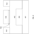
- FIG. 4 is a schematic diagram of one embodiment of a three-terminal field effect switch.
- the switch includes a source 412, a drain 414, and a channel layer comprising vanadium dioxide 402 disposed between source 412 and drain 414.
- a gate stack comprising a gate dielectric 416 and a gate contact 418 is disposed on channel layer 402.
- a second layer of vanadium dioxide 404 underlies channel layer 402.
- the second layer of vanadium dioxide 404 has a lower rutile-to-monoclinic structural transition temperature than channel layer 402.
- the field effect switch also includes a dielectric substrate 407.
- the vanadium dioxide of channel layer 402 When the switch is at a temperature below its electronic transition temperature, the vanadium dioxide of channel layer 402 is in an electrically insulating monoclinic phase and current is unable to flow between source 412 and drain 414. However, when a gate voltage is applied to gate contact 418, the vanadium dioxide of channel layer 402 is converted into a metallic monoclinic phase, the switch is turned on and current is able to flow between the source and the drain.
- the vanadium dioxide layer having the lower structural transition temperature can be composed of, for example, tungsten-doped vanadium dioxide and the vanadium dioxide layer having the higher structural transition temperature can be composed of, for example, stoichiometric VO 2 .
- both layers can be extrinsically doped, provided that the first layer retains a lower rutile-to-monoclinic phase transition than the second layer.
- This example demonstrates a purely electronically-driven metal-insulator transition that keeps the crystalline structure of vanadium dioxide (VO 2 ).
- a general framework is proposed for stabilizing a metallic monoclinic phase and demonstrating the reversible phase transition between the metallic and insulating monoclinic phases in VO 2 .
- VO 2 displays intrinsic phase coexistence in the vicinity of phase transition.
- a heterostructure was conceived between the rutile and monoclinic phases ( FIG. 5A ), where electronic correlations and the interfacial energy would favor the metallic monoclinic phase.
- the first-principles density functional theory (DFT) calculations predicted the metallic nature of the monoclinic layer in the rutile/monoclinic heterostructure ( FIG. 5B ), distinct from the insulating nature of the bulk monoclinic VO 2 .
- DFT density functional theory
- FIG. 5D shows the total energy of the rutile/monoclinic heterostructure, obtained by phase-field simulations, as a function of the thickness t m of the monoclinic layer.
- the interfacial energy between metallic rutile and metallic monoclinic phases was naturally smaller to that between metallic rutile and insulating monoclinic phases in the phase-field model, due to the homogeneous ⁇ EC in the former case.
- a nanoscale bilayer composed of two VO 2 layers was designed with different transition temperatures (namely, Ti and T 2 ; FIG. 6A ).
- the rutile/monoclinic heterostructure can occur at intermediate temperatures between Ti and T 2 .
- an intrinsic point defect was utilized, i.e., oxygen vacancy and the resulting electron doping.
- Introducing a minute amount of oxygen vacancies enabled the lowering of the transition temperature of VO 2 without compromising the sharp metal-insulator transition.
- the low angle annular dark field (LAADF) image is very sensitive to the strain fields from oxygen vacancies, while the high angle annular dark field (HAADF) image is dominated by the (high-Z) cation sites.
- the HAADF image (left in FIG. 6B ) obtained showed little intensity change across the VO 2- ⁇ /VO 2 interface (denoted by white dashed lines).
- the LAADF image (right in FIG. 6B ) displayed a noticeable, abrupt intensity change across the VO 2- ⁇ /VO 2 interface, making the oxygen deficiency in the VO 2- ⁇ layer visible.
- This two-step structural phase transition can be explained by two separate structural transitions, i.e., at T ⁇ 279 K for the top VO 2- ⁇ layer and at T ⁇ 287 K for the bottom VO 2 layer.
- T ⁇ 279 K for the top VO 2- ⁇ layer
- T ⁇ 287 K for the bottom VO 2 layer.
- the top VO 2- ⁇ and bottom VO 2 layers have rutile and monoclinic structures, respectively, which forms the desired rutile/monoclinic heterostructure, as illustrated in the inset of FIG. 7B .
- the electronic phase transition in the VO 2- ⁇ /VO 2 bilayer was explored by measuring the electrical resistivity ( FIG. 8A ) and carrier concentration.
- the bilayer showed a single-step, collective metal-insulator transition at T ⁇ 279 K.
- the electronic phase transition of the bilayer looked nearly identical to that of a VO 2- ⁇ single layer (black dotted line in FIG. 8A ), which means that in the VO 2- ⁇ /VO 2 bilayer, the electronic phase (i.e., metallic or insulating) of the VO 2 layer collectively followed that of the VO 2- ⁇ layer.
- LDA local density approximation
- LDA + U semi-empirical + Hubbard U
- FIG. 9B shows a layer-resolved profile of the density of states (DOS) in the superlattice.
- DOS density of states
- the density of states was calculated by capturing local monoclinic structures within the monoclinic region of the superlattice ( FIG. 10A and 10B ), and the local structural modification itself was found to not cause any metallicity in monoclinic VO 2 . This result excludes the main contribution of the interfacial structural relaxation and indicates a purely electronic origin behind the metallization of monoclinic VO 2 .
- E HS is the total energy of the superlattice
- E HS,fix is the total energy of the superlattice before relaxation
- A is the in-plane lateral area of a unit cell
- a factor of two takes into account the presence of two interfaces in the superlattice.
- the calculated interface energy E i,rel was found to be small E i,rel ⁇ 60 mJ m -2 , comparable to accuracy of the calculations. This value is much smaller than typical interfacial energies ⁇ 1 J m -2 in metal/insulator interfaces.
- FIGs. 11A and 11B show the calculated density of states of hole-doped and electron-doped monoclinic VO 2 , respectively, at hole/electron concentrations of 0.025 (top panels), 0.25 (middle panels), and 0.5 (bottom panels). It was found that increasing hole concentration caused a significant band gap narrowing, whereas the electron doping did not affect the gap much. The gap decreased with the increasing hole doping (i.e., lower d band occupation) and finally collapsed at high hole doping, which can be interpreted as the decrease in the strength of electron correlation. Notably, the density of states of the hole-doped monoclinic VO 2 looked similar to that of the metallic monoclinic region in the rutile/monoclinic superlattice ( FIG. 5B ).
- the metal-insulator and structural transition in VO 2 can be characterized by an electron-correlation order parameter ⁇ EC and a structural order parameter ⁇ S , respectively.
- ⁇ EC denotes the electron spin density correlation between the electrons of two adjacent V atoms
- ⁇ S characterizes the dimerization of the V atoms.
- a 1 , b 1 , c 1 , a 2 , b 2 , c 2 , g 1 , and g 2 are coefficients of the Landau polynomial, and are fitted based on the critical temperature and the entropy of transformation measured in this work and other experiments.
- the gradient energy is taken into account
- F grad ⁇ d 3 r 1 2 k 1 ⁇ ⁇ EC 2 + 1 2 k 2 ⁇ ⁇ S 2 , where k 1 and k 2 are the gradient energy coefficients of ⁇ EC and ⁇ S , respectively.
- the gradient energy coefficients k 1 and k 2 are positive and fitted to the interfacial energy of 50 mJ m -2 , which was arbitrarily chosen between an experimental estimation of 25 mJ m -2 and a calculated upper bound of ⁇ 60 mJ m -2 from the DFT simulation.
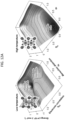
- FIG. 12A The energy landscapes of the bulk Landau potential at a low temperature and a high temperature are shown in FIG. 12A in the left and right panels, respectively.
- the transition temperature T PT the transition temperature
- the metastable metallic monoclinic phase disappears below T m ⁇ T PT - 12 K.
- FIG. 12B shows the temperature dependence of ⁇ S and ⁇ EC .
- phase-field simulations were employed to confirm the above hypothesis.
- VO 2 epitaxial thin films were grown on a rutile TiO 2 (001) substrate using the pulsed laser deposition (PLD) method.
- PLD pulsed laser deposition
- a KrF excimer laser (248 nm) beam was focused on the vanadium metal target to an energy density of ⁇ 2.0 J cm -2 and pulsed at 10 Hz.
- VO 2 films were grown at a substrate temperature of 300 °C and oxygen partial pressures ( P O2 ) ranging from 12 to 24 mTorr.
- P O2 oxygen partial pressures
- the stoichiometric VO 2 and slightly oxygen-deficient VO 2- ⁇ films were deposited at P O2 of 21 and 18 mTorr, respectively. [The ⁇ value was roughly estimated to be -0.01 ( FIG.
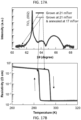
- FIGS. 15A-15C represent the results of XRD 2 ⁇ - ⁇ scans, rocking curve, and reciprocal space mapping (RSM), respectively, for the VO 2 films.
- the full width at half maximum (FWHM) of rocking curve was measured as small as 0.017° ( FIG. 15B ), indicating the excellent crystalline quality of VO 2- ⁇ /VO 2 bilayer.
- FWHM full width at half maximum
- FIG. 15C From the RSM data ( FIG. 15C ), it was confirmed that the VO 2- ⁇ /VO 2 bilayer is fully coherent with the TiO 2 substrate without any strain relaxation.
- Film surfaces were imaged by atomic force microscopy (AFM; FIG. 15D ).
- the concentration of oxygen vacancies in the films was roughly estimated from the measured unit-cell volume.
- r M the ionic radius of the cation
- V the unit cell volume
- a and B constants.
- r V4+ and r V3+ are the ionic radii of V 4+ and V 3+ , respectively.
- 17A and 17B exhibit the XRD and transport data, respectively, for those samples, showing negligible change in sample properties even after the additional annealing at the reduced P O2 . This indicate that while the P O2 variation during growth affects the oxygen stoichiometry and the resulting metal-insulator transition of VO 2 films, the P O2 variation after growth doesn't affect those much.
- VO 2- ⁇ and VO 2 layer in the bilayer affects the phase transitions
- two different bilayers were grown, i.e., VO 2- ⁇ /VO 2 and VO 2 /VO 2- ⁇ bilayers, on TiO 2 (001) substrate.
- P O2 18 mTorr
- the sequence of VO 2- ⁇ and VO 2 layer in the bilayer didn't induce any change in phase transitions.
- the metal-insulator transitions of both the VO 2- ⁇ /VO 2 and VO 2 /VO 2- ⁇ bilayers follow that of the VO 2- ⁇ single layer.
- the thin, electron-transparent sample was prepared using the conventional method (mechanical thinning to -10 ⁇ m or less; and ion beam milling to electron transparency at an acceleration voltage of 0.5-3.5 kV using an Ar ion beam).
- the atomic structures were observed using a STEM (JEOL JEM-2100F, JEOL Ltd., Japan) with an aberration corrector (CEOS GmbH, Heidelberg, Germany); and its probe diameter and convergence angle of the beam were -0.9 ⁇ and - 24 mrad under the acceleration voltage of 200 kV, respectively.
- the collection semiangles of the detectors for high angle annular dark field (HAADF) and low angle annular dark field (LAADF) imaging were greater than 80-200 and 30-60 mrad, respectively.
- the obtained STEM images were local wiener filtered to reduce background noise (HREM Research Inc., Japan).
- LAADF can provide the qualitative information of the atomic dechanneling mainly caused by the strain or the vacancies due to the low-order diffractions of electrons, close to the on-axis.
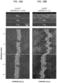
- FIGs. 18A and 18B the HAADF and LAADF contrasts, respectively, were profiled for better visualization, wherein the stronger LAADF contrast from the upper half indicates the existence of oxygen vacancies.
- LAADF image confirms that the film consists of VO 2 and VO 2- ⁇ layers.
- the metal-insulator transition in VO 2 films was monitored by measuring their electrical resistivity as a function of temperature. Electrical resistivity was measured using a four-contact van der Pauw technique. For the transport measurements, both indium and aluminum metal contacts were tried, but little change was found in the data.
- the metal-insulator transition (e.g., the transition temperature) of VO 2- ⁇ /VO 2 bilayer was found to be almost identical to that of VO 2- ⁇ single layer ( FIG. 8A ). If the VO 2 and VO 2- ⁇ layers in the bilayer are independent of each other without any interaction, there should be a clear two-step signature in the metal-insulator transition, as shown in FIG. 21A .
- the interfacial effect was intentionally suppressed by inserting an ultrathin ( ⁇ 2 nm) TiO 2 layer between VO 2- ⁇ and VO 2 .
- the VO 2- ⁇ /TiO 2 /VO 2 trilayer showed a clear two-step metal-insulator transition ( FIG. 21B ), which verified the interfacial effect as the intrinsic origin of the collective, single-step metal-insulator transition in the VO 2- ⁇ /VO 2 bilayer.
- Raman spectra of VO 2 thin films grown on TiO 2 (001) substrates have been measured in backscattering geometry normal to the film surface using a Jobin Yvon T64000 triple spectrometer equipped with a liquid nitrogen cooled multichannel charge coupled device detector. Several excitation wavelengths were tried, visible (442 and 488 nm), and UV (325 and 363.8 nm). It was found that with visible excitation the spectra are dominated by the substrate signal. 363.8-nm excitation was chosen as it resulted in a stronger signal from VO 2 films. Spectra were measured in the temperature range 250-300 K using a variable temperature closed cycle helium cryostat.
- the high-temperature metallic phase of bulk VO 2 had a tetragonal rutile structure with space group D 4 h 14 ( P 4 2 / mnm ) and four Raman-active phonons.
- metallic phase the phonon peaks were very broad and weak; they were hardly observable even in the bulk.
- the spectra above the transition temperature contained the TiO 2 substrate features only.
- the low-temperature phase had a monoclinically distorted structure with space group C 2 h 5 ( P 2 1 / c ).
- the unit cell doubled in size in the monoclinic phase, which had 18 Raman-active phonons (9 A g and 9 B g modes).
- a g modes could be distinguished at 151, 225, 196, 316, 393, 457, and 499 cm -1 (two more A g modes that should appear around 595 and 618 cm -1 are masked by strong peak of the TiO 2 substrate at 612 cm -1 ). Also, three B g modes could be seen at 335, 437, and 812 cm -1 ; the others were either too weak or overlapped by the substrate features.
- the temperature dependence of the relative Raman intensity of the two most intensive VO 2 peaks (i.e., ⁇ 2 and ⁇ 3 near 196 and 316 cm -1 ) was obtained, which originated from the monoclinic distortion in VO 2 ( FIG. 7B ).
- the integrated intensities of these peaks were normalized by the integrated intensity of the 612 cm -1 peak of TiO 2 substrate.
- VO 2 was in the tetragonal rutile phase, and the intensity of the monoclinic VO 2 peaks was essentially zero.
- the Raman peaks of monoclinic VO 2 appeared suddenly during the rutile-to-monoclinic structural phase transition ( FIGS. 7A and 7B ).
- the Raman spectroscopy measurements showed that the VO 2- ⁇ /VO 2 bilayer had a two-step structural phase transition ( FIG. 7B ), whereas the VO 2 single layer had a single-step structural phase transition ( FIG. 22 ).
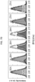
- the rutile-to-monoclinic structural phase transition was monitored by conducting X-ray diffraction (XRD) (00L) scans on cooling at 300K ( FIG. 7D , top panel), 284 K ( FIG. 7D , middle panel), and 272 K ( FIG. 7D , bottom panel). Before the measurement, the sample was aligned using the (002) reflection of the TiO 2 substrate. Due to the increased out-of-plane lattice during monoclinic distortion, the center L (Reciprocal Lattice Units-RLU) position of the XRD peaks was shifted from ⁇ 2.080 (for high-temperature rutile) to ⁇ 2.072 (for low-temperature monoclinic).
- XRD X-ray diffraction
- the measured XRD peaks were fitted using two Gaussian curves (shown in FIG. 7D ) with the L values of 2.080 ⁇ 0.0005 RLU (for rutile) and 2.072 ⁇ 0.0005 RLU (for monoclinic).
- the relative monoclinic portion was estimated to be A Mc /( A Mc + A R ), where A R and A Mc correspond to the area under the two fitted Gaussian curves.
- the maximum peak intensity was normalized with the value at 300 K.
Landscapes
- Chemical & Material Sciences (AREA)
- Crystallography & Structural Chemistry (AREA)
- Inorganic Compounds Of Heavy Metals (AREA)
- Semiconductor Integrated Circuits (AREA)
- Compositions Of Oxide Ceramics (AREA)
- Inorganic Insulating Materials (AREA)
- Thermistors And Varistors (AREA)
Description
- Understanding metal-insulator transitions in strongly correlated materials is one of the major challenges in condensed matter physics, with implications for both fundamental science and technology. Correlated materials exhibit strong coupling between charge, spin, and lattice degrees of freedom, so that the metal-insulator transition is almost always accompanied by an associated structural phase transition. This coexistence obscures the underlying physics, making it difficult to disentangle different intrinsic interactions controlling the metal-insulator transition. Furthermore, the structural transition generally limits the ultimate switching speed and endurance of novel ultrafast electronic applications based on the metal-insulator transition in these correlated materials. A predictive guideline for achieving an isostructural metal-insulator transition is of great interest from both the fundamental and technological points of view.
- VO2 is an example of a correlated oxide material with a near-room-temperature metal-insulator transition (341 K in bulk). A device including a thin film having a plurality of layer regions distributed in the direction of the thicknesses thereof, wherein the layer regions are made of non-doped VO2 and VO2 doped with at least one of W, Nb, Mo and Ti is provided in
US 2014/085044-A1 .
However, the transition from metallic to insulating phase in VO2 is accompanied by a structural transition from the higher-symmetry rutile structure to the lower-symmetry monoclinic structure via the formation of V-V dimers. This arises from the inherently coupled electronic and structural phases of bulk VO2. - The present invention is defined in the independent claims. Preferred embodiments are defined in the corresponding dependent claims.
- Heterostructures that include a bilayer composed of epitaxial layers of vanadium dioxide having different rutile-to-monoclinic structural transition temperatures are provided. Also provided are electrical switches that incorporate the heterostructures.
- One embodiment of a bilayer includes: (a) a first layer of vanadium dioxide characterized in that it undergoes a rutile-to-monoclinic structural phase transition at a first structural transition temperature; and (b) a second layer of vanadium dioxide adjacent to the first layer of vanadium dioxide. The second layer of vanadium dioxide is characterized in that it undergoes a rutile-to-monoclinic structural phase transition at a second structural transition temperature that is higher than the first structural transition temperature. The second layer of vanadium dioxide has a metallic monoclinic phase at a temperature between the first structural transition temperature and the second structural transition temperature.
- One embodiment of a method of inducing a single-step metal-insulator electronic transition in a bilayer of the type described herein includes: maintaining the bilayer at a temperature above the first structural transition temperature; and applying an external stimulus to the bilayer, wherein the external stimulus induces the second layer of vanadium dioxide to undergo an isostructural electronic phase transition from an electrically insulating monoclinic crystalline phase to an electrically conducting monoclinic crystalline phase.
- One embodiment of an electrical switching device includes a bilayer comprising: a first layer of vanadium dioxide characterized in that it undergoes a rutile-to-monoclinic structural phase transition at a first structural transition temperature; and a second layer of vanadium dioxide adjacent to the first layer of vanadium dioxide, the second layer of vanadium dioxide characterized in that it undergoes a rutile-to-monoclinic structural phase transition at a second structural transition temperature that is higher than the first structural transition temperature, wherein the second layer of vanadium dioxide has a metallic monoclinic phase at a temperature between the first structural transition temperature and the second structural transition temperature. The device further includes a first electrically conducting contact in electrical communication with a first area of the bilayer; a second electrically conducting contact in electrical communication with a second area of the bilayer; and an external stimulus source configured to apply a metal-insulator transition-inducing external stimulus to the bilayer.
- Other principal features and advantages of the invention will become apparent to those skilled in the art upon review of the following drawings, the detailed description, and the appended claims.
- Illustrative embodiments of the invention will hereafter be described with reference to the accompanying drawings, wherein like numerals denote like elements.
-
FIG. 1 is a schematic diagram showing the off-on switching of a vanadium dioxide bilayer. -
FIG. 2 is a schematic diagram of a parallel plate capacitor that incorporates a vanadium dioxide trilayer. -
FIG. 3 is a schematic diagram of a planar switch that incorporates a vanadium dioxide bilayer. -
FIG. 4 is a schematic diagram of a field-effect switch that incorporates a vanadium dioxide bilayer. -
FIGS. 5A-5F depict the emergence of stable metallic monoclinic VO2 phase.FIG. 5A shows the rutile/monoclinic heterostructure used in the DFT calculation, including V atoms (rutile VO2 and monoclinic VO2).FIG. 5B depicts the calculated density of states of the local monoclinic region [denoted by (a) in A] in the rutile/monoclinic heterostructure. The density of states of bulk monoclinic VO2 is also shown as a reference.FIG. 5C shows the free energy landscape of bulk VO2 at 287 K, just below the transition temperature.FIG. 5D depicts the total energies as a function of tm in the rutile/monoclinic heterostructureFIG. 5E shows stable states of the rutile/monoclinic heterostructure for tm > tc.FIG. 5F shows stable states of the rutile/monoclinic heterostructure for tm < tc. The arrows represent the two-component order parameter (η S, η EC), and the shading represents the norm (η S 2 + η EC 2)0.5. -
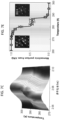
FIGS. 6A-6B show the design of an artificial VO2-δ /VO2 bilayer.FIG. 6A depicts electrical resistivity measured as a function of temperature of 8-nm-thick epitaxial VO2 and VO2-δ (roughly, δ ~ 0.01) single layer films on (001) TiO2 substrates.FIG. 6B shows atomic-scale imaging of oxygen vacancy profile in the VO2-δ /VO2 bilayer (inset). The lines indicate measured contrast profile through atomic columns and white dashed lines represent a nominal interface between VO2 and VO2-δ . -
FIG. 7A-7E depict structural phase transition in VO2-δ /VO2 bilayer.FIG. 7A shows Raman spectra of VO2-δ (8 nm)/VO2 (8 nm) bilayer at various temperatures. Raman peaks from the monoclinic distortion are denoted by ω 1, ω 2, and ω 3.FIG. 7B shows the relative monoclinic portion as a function of temperature, estimated from monoclinic Raman intensity inFIG. 7A . The inset depicts a schematic for atomic structure of VO2-δ /VO2 bilayer at intermediate temperatures.FIG. 7C shows an X-ray diffraction (XRD) (00L) scan around the TiO2 (002) Bragg peak, measured on cooling.FIG. 7D shows representative XRD peaks at temperatures of 300, 284, and 272 K. InFIG. 7E experimental data (open circles) are fitted using Gaussian curves (solid lines). The relative monoclinic portion, as a function of temperature, is estimated from the XRD peak analysis inFIG. 7D . The insets show the measured electron diffraction patterns of the bilayer at low and high temperatures. -
FIGS. 8A-8C depict isostructural metal-insulator transition in VO2-δ /VO2 bilayer.FIG. 8A shows electrical resistivity vs. temperature of VO2-δ (8 nm)/VO2 (8 nm) bilayer (solid line) and 8-nm-thick VO2-δ single layer (black dashed line), measured on cooling. Metallic and insulating phases are represented by red and blue colors, respectively.FIG. 8B depicts the monoclinic portion (fromFIGS. 7B and7E ) as a function of temperature.FIG. 8C shows the temperature dependence of the monoclinic Raman shift, i.e., ω 2 and ω 3, shown inFIG. 7A . -
FIGS. 9A and 9B show the calculated electronic structure of the rutile/monoclinic heterostructure.FIG. 9A depicts the calculated atomic structure for 6-unit-cells (including 23 planes of VO2) of monoclinic VO2, sandwiched by rutile VO2. While the atomic positions of the two-unit-cell monoclinic region were fixed near the lower interface as bulk-like, full atomic relaxation was allowed in all other monoclinic regions.FIG. 9B shows the calculated density of states for each layer as a function of energy E - E F. Gray color indicates the regions that have the density of states, lower than 0.05. The values of the V-V-V bond angle are also represented along the [001] Rutile axis, an indication of monoclinic distortion, for each layer by open red squares. -
FIGS. 10A and 10B show the density-of-states calculation for the captured local monoclinic structure.FIG. 10A shows a local monoclinic structure (denoted by M1, M2, M3, M4, and M5) in the rutile/monoclinic superlattice, which was then used as a bulk structure for the density of states calculation.FIG. 10B shows calculated density of states for a bulk monoclinic employing the captured local monoclinic structures. -
FIGS. 11A and11B show the calculated electronic structure of hole- and electron-doped monoclinic VO2.FIG. 11A shows the calculated density of states of hole-doped monoclinic VO2, which shows a significant band-gap narrowing as the hole concentration increases.FIG. 11B shows the calculated density of states of electron-doped monoclinic VO2, which shows a negligible band-gap narrowing as the electron concentration increases. -
FIGS. 12A and12B depict simulated phase transitions in bulk VO2.FIG. 12A shows the free energy landscape of bulk VO2 at 287 K (left) and 292 K (right).FIG. 12B shows the temperature dependence of η S and η EC, which make the global minimum in free energy (i.e., equilibrium phase) at each temperature. -
FIGS. 13A-13C show the emergence of a stable metallic monoclinic phase.FIG. 13A is a schematic of the bulk molar Landau potential, showing the non-equilibrium (metastable) metallic monoclinic phase, as well as the equilibrium (stable) insulating monoclinic phase.FIG. 13B is a schematic of the total energy per area as a function of thickness in the rutile/monoclinic heterostructure.FIG. 13C shows stable states, calculated by phase-field simulations, of the VO2-δ /VO2 bilayer for temperatures of T = 291 K, 283 K, and 277 K. The arrows represent the two-component order parameter (η S, η EC), and the shading represents the norm (η S 2 + η EC 2)0.5. The thickness of each layer was set to be below t c ~ 9.4 nm. -
FIGS. 14A and 14B show the growth of the VO2-δ /VO2 bilayer. By changing the oxygen partial pressure (P O2) during film growth [as shown inFIG. 14A ], the VO2-δ /VO2 bilayer nanostructure can be prepared [as shown inFIG. 14B ], which has two distinct transition temperatures in its upper (i.e., VO2-δ ) and lower (VO2) layers. -
FIGS. 15A-15D show structural characterization of VO2-δ /VO2 bilayer.FIG. 15A shows X-ray diffraction (XRD) 2θ-ω scans of VO2 single layer, VO2-δ single layer, and VO2-δ /VO2 bilayer. The simulated result for VO2-δ /VO2 bilayer is also represented, which is well matched with the experimental data.FIG. 15B shows the rocking curve of the XRD (002) reflection for VO2-δ /VO2 bilayer.FIG. 15C shows an XRD reciprocal space map around the (112) reflections of TiO2 substrate and VO2-δ /VO2 bilayer.FIG. 15D is an atomic force microscopy image of VO2-δ /VO2 bilayer, showing smooth surface of the film. -
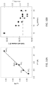
FIGS. 16A and 16B show a rough estimation of oxygen stoichiometry.FIG. 16A shows the linear relationship between r M and V 1/3 in rutile oxides.FIG. 16B shows the measured unit cell volume and the estimated oxygen-vacancy concentration δ in the VO2 films, as a function of oxygen partial pressure (P O2) used during film growth. -
FIGS. 17A and 17B show no effect of the "after-growth" change of P O2.FIG. 17A shows X-ray diffraction (XRD) 2θ-ω scans of two VO2 samples. One line is for the sample that was grown and cooled at P O2 = 21 mTorr. Another line is for the sample that was grown at P O2 = 21 mTorr, annealed for 10 minutes at a reduced P O2 = 17 mTorr, and cooled at P O2 = 17 mTorr.FIG. 13B shows electrical resistivity as a function of temperature for two VO2 samples inFIG. 17A . -
FIGS. 18A and 18B depict nanoengineered oxygen stoichiometry.FIG. 18A shows a high-angle annular dark field (HAADF) image andFIG. 18B shows a low-angle annular dark field (LAADF) image, both of which are sensitive to V atomic lattice and oxygen vacancy, respectively. Thin, solid lines indicate measured contrast profile through atomic columns and white dashed lines represent a nominal interface between VO2 and VO2-δ .FIG. 18C shows a derivative of the fitted line (thick solid) for the LAADF contrast profile in B. -
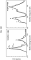
FIGS. 19A-19C show an EELS analysis of oxygen stoichiometry.FIG. 19A is an LAADF-STEM image of a VO2-δ /VO2 bilayer.FIG. 19B shows measured V-L 2,3 (a and b peaks) and O-K edges (c, d, and e peaks) for the top VO2-δ and bottom VO2 layers of VO2-δ /VO2 bilayer.FIG. 19C shows calculated EELS data for the vanadium L 2,3 (left) and oxygen K (right) edges. -
FIGS. 20A and 20B show transport measurement.FIG. 20A shows electrical resistivity as a function of temperature on cooling for VO2-δ (8 nm)/VO2 (8 nm) bilayer, VO2 (8 nm)/VO2-δ (8 nm) bilayer, and 8-nm-thick VO2-δ single layer (black dotted line).FIG. 20B shows carrier concentration as a function of temperature on cooling for VO2-δ (8 nm)/VO2 (8 nm) bilayer. The black solid line is the guide to the eyes. -
FIGS. 21A and 21B show the metal-insulator transition of the trilayer.FIG. 21A shows the predicted metal-insulator transition on cooling for the simply parallel-connected 8-nm-thick VO2 and 8-nm-thick VO2-δ layers without any interfacial interaction.FIG. 21B shows measured metal-insulator transition on cooling for the VO2-δ (8 nm)/TiO2 (2 nm)/VO2 (8 nm) trilayer. -
FIG. 22 depicts metal-insulator and structural phase transitions of the VO2 single layer. Metal-insulator and structural phase transitions, measured on cooling in VO2 single layer, show a single-step feature. - Heterostructures that include a bilayer composed of epitaxial layers of vanadium dioxide having different rutile-to-monoclinic structural transition temperatures are provided. Also provided are electrical switches that incorporate the heterostructures. The bilayers are characterized in that they undergo a single-step, collective, metal-insulator transition at an electronic transition temperature, Telectric. At temperatures below Telectric, the layer of vanadium dioxide having the higher structural transition temperature comprises an insulating monoclinic crystalline phase, which is converted to a metallic monoclinic crystalline phase at temperatures above Telectric. Because Telectric can be close to room temperature, the bilayers are well-suited for near room temperature switching applications.
- In the bilayers, the first of the two layers of vanadium dioxide is engineered to have a lower structural transition temperature than the second of the two layers. This can be accomplished by extrinsically doping the vanadium dioxide or introducing oxygen vacancies in the vanadium dioxide of the first layer. The vanadium dioxide bilayers may be grown epitaxially on a growth substrate, such as a TiO2 substrate, beginning with a stoichiometric layer of VO2 upon which an extrinsically-doped or oxygen-deficient layer of vanadium dioxide is grown. Extrinsic dopants that can be introduced into the vanadium dioxide in order to lower its structural transition temperature include metal dopants, such as tungsten, molybdenum, chromium, and niobium. A typical dopant concentration is 0.01 ≤ x ≤ 0.1 for the doped vanadium dioxide, V1-x M x O2. Alternatively, oxygen vacancies can be introduced into the vanadium dioxide to produce non-stoichiometric, oxygen-deficient VO(2-δ) by carrying out epitaxial growth under a reduced oxygen partial pressure. By way of illustration only, in some embodiments of the bilayers, δ is in the range from about 0.005 to 0.02.
- For the purposes of this disclosure the term vanadium dioxide refers to stoichiometric VO2 and also to non-stoichiometric, extrinsically doped vanadium dioxide (V(1-x)DxO2), in which dopant atoms (D) are substituted for a portion of the vanadium atoms, and also to non-stoichiometric, oxygen-deficient vanadium dioxide comprising oxygen vacancies (VO(2-δ)).
- The resulting extrinsically doped or oxygen-deficient VO(2-δ) is characterized in that it undergoes a rutile-to-monoclinic structural phase transition at a lower structural transition temperature than does stoichiometric VO2. This produces a two-step structural phase transition in the bilayer. Like the single-step, collective, electronic phase transition, the structural phase transitions can occur at temperatures near room temperature. For example, in some embodiments of the bilayers, the electronic transition temperature is in the range from about 274 K to about 284 K, the rutile-to-monoclinic structural phase transition for the first layer of vanadium dioxide is in the range from about 274 K to about 284 K, and the rutile-to-monoclinic structural phase transition for the second layer of vanadium dioxide is in the range from about 282 K to about 292 K. (Unless otherwise indicated, the structural and electronic phase transition temperatures referred to in this disclosure refer to the transition temperatures in the absence of an applied external field or strain.)
- Without intending to be bound to any particular theory of the invention, it is proposed that the isostructural electronic transition in the monoclinic vanadium dioxide can be attributed to an interfacial energy contribution in the bilayer that stabilizes a non-equilibrium metallic monoclinic crystalline phase. Because the metal-insulator electronic phase transition of the bilayer is not accompanied by a rutile-to-monoclinic structural phase transition, switches incorporating the bilayers can have improved electronic switching speeds and durabilities, relative to switches in which the electronic metal-insulator transition is the result of a rutile-to-monoclinic phase change. In order to stabilize the metallic monoclinic phase in the bilayer, the layer of vanadium dioxide that undergoes the isostructural electronic transition should be sufficiently thin that the interfacial energy contribution dominates the bulk energy contribution in the structure, as discussed in detail in the Example. Embodiments of the bilayers include those in which the layer of vanadium dioxide having the higher rutile-to-monoclinic structural transition temperature has a thickness of less than 10 nm, including a thickness of less than 9.5 nm. In some embodiments of the bilayers, both layers meet these thickness criteria.
- The vanadium dioxide bilayers can be characterized by sharp, single-step metal-insulator electronic phase transitions, where the sharpness of a transition is characterized by the full width at half maximum (FWHM) of the derivative curve of a heating curve. Some embodiments of the bilayers have an electronic phase transition sharpness of 3 K or less. This includes bilayers having an electronic phase transition sharpness of 2 K or less, and further includes bilayers having an electronic phase transition sharpness of 1 K or less. The electronic phase transition is accompanied by a large drop in the bilayer's magnitude of electrical resistance (ΔR). Some embodiments of the bilayers have a ΔR of at least 2 orders of magnitude. This includes bilayers having a ΔR of at least 3 orders of magnitude, and further includes bilayers having a ΔR of at least 4 orders of magnitude.
- The bilayers can be incorporated into multilayered device structures having three or more layers, wherein the additional layers may be composed of vanadium dioxide or other materials. For example, a bilayer may be part of a trilayer structure in which the layer of vanadium dioxide having a lower structural phase transition temperature is sandwiched between a pair of vanadium dioxide layers having a higher structural transition temperature, or vice versa. The layers in the bilayer or multilayer structures need not have the same shape or dimensions and a given layer need not completely cover the surface of its adjacent layer(s) in the structure. Thus, the individual layers that make up the bilayer and the overall shape of the bilayer may take on a variety of geometries, provided that the two layers that make up the bilayer form an interface that is capable of stabilizing a metallic monoclinic crystalline phase within the bilayer.
- A schematic diagram illustrating the operation of a bilayer as a thermally activated switch is provided in
FIG. 1 . Initially, the switch is in an off-state (1) at an operating temperature above the structural transition temperature of the first layer of vanadium dioxide 101 (Tstruct1), but below the bilayer's electronic transition temperature (Telectric). In the off-state, the second layer ofvanadium dioxide 102 comprises an insulating monoclinic crystalline phase. The switch can be converted into its on-state (2) by heating the bilayer to a second operating temperature that is above Tstruct1 and also above Telectric. In the on-state, second layer ofvanadium dioxide 102 comprises a metallic monoclinic crystalline phase. In a reverse switching cycle, the bilayer can be cooled from the second operating temperature to a temperature below Telectric, but above Tstruct1 to return the switch to its off-state. - Although the switching of a bilayer is illustrated with respect to a thermally-activated switch in
FIG. 1 , other means of activation can be used. That is, external stimuli, other than heating and cooling, can be used to induce the bilayer's electronic phase transition. For example, an electric field, an optical field, a mechanical strain, or a combination thereof, can be applied to the bilayer to induce the electronic phase transition by shifting Telectric. These stimuli can be applied using a temperature modulator, a voltage source, a light source, or a stain modulator, each configured to apply its respective stimulus to the bilayer. - The bilayers can be incorporated into a variety of electrical switching structures, including capacitors, planar switches, and field effect switches, for a variety of switching applications. For example, the bilayers can be used in circuits, including integrated circuits, for memory devices (e.g., CMOS chips) and communication devices. In each of these devices, the conversion of the bilayer from its electrically insulating to its electrically conducting metallic state, and vice versa, changes the resistance (and, therefore, conductance) of the bilayer, thereby modulating the device's current flow or capacitance. One embodiment of a parallel plate capacitor is shown schematically in
FIG. 2 . The capacitor includes three layers of vanadium dioxide on asupport substrate 201, wherein a middle layer ofvanadium dioxide 202 is sandwiched between two other layers ofvanadium dioxide Middle layer 202 has a higher rutile-to-monoclinic structural transition temperature thanlayers vanadium dioxide layer 202 is in an electrically insulating state, the device has a high capacitance, and charges build up on outer vanadium dioxide layers 204 and 206. However, when an electronic phase transition-inducing stimulus is applied to the capacitor, converting thevanadium dioxide layer 202 into its metallic state, the capacitance of the device drops and outer vanadium dioxide layers 204 and 206 are able to discharge throughlayer 202. The stimulus may be, for example, a voltage applied across the structure by a voltage source connected between vanadium dioxide layers 204 and 206. - One embodiment of a planar switch is shown schematically in
FIG. 3 . The switch includes a channel layer ofvanadium dioxide 302 bridging a first contact layer ofvanadium dioxide 304 and a second contact layer ofvanadium dioxide 306 on asupport substrate 301. First and second contact layers 304 and 306 have a lower rutile-to-monoclinic structural transition temperature thanchannel layer 302. When the switch is maintained at a temperature above the structural transition temperature of first and second contact layers 304 and 306, those layers will comprise metallic rutile vanadium dioxide and, therefore, can act as electrically conductive (metallic) electrodes for the switch. When the switch is at a temperature below its electronic transition temperature, the vanadium dioxide ofchannel layer 302 is in an electrically insulating monoclinic phase and current is unable to flow between first and second contact layers 304 and 306. However, when an electronic phase transition-inducing stimulus is applied to the switch, convertingvanadium dioxide layer 302 into a metallic monoclinic state, the switch is turned on and current is able to flow between the contact layers. The stimulus may be, for example, a voltage applied across the structure by a voltage source connected between vanadium dioxide contact layers 304 and 306. -
FIG. 4 is a schematic diagram of one embodiment of a three-terminal field effect switch. The switch includes asource 412, adrain 414, and a channel layer comprisingvanadium dioxide 402 disposed betweensource 412 and drain 414. A gate stack comprising agate dielectric 416 and agate contact 418 is disposed onchannel layer 402. A second layer ofvanadium dioxide 404 underlieschannel layer 402. The second layer ofvanadium dioxide 404 has a lower rutile-to-monoclinic structural transition temperature thanchannel layer 402. The field effect switch also includes a dielectric substrate 407. When the switch is at a temperature below its electronic transition temperature, the vanadium dioxide ofchannel layer 402 is in an electrically insulating monoclinic phase and current is unable to flow betweensource 412 and drain 414. However, when a gate voltage is applied togate contact 418, the vanadium dioxide ofchannel layer 402 is converted into a metallic monoclinic phase, the switch is turned on and current is able to flow between the source and the drain. - In the switching devices of
FIGS. 2 - 4 , the vanadium dioxide layer having the lower structural transition temperature can be composed of, for example, tungsten-doped vanadium dioxide and the vanadium dioxide layer having the higher structural transition temperature can be composed of, for example, stoichiometric VO2. In some embodiments of the bilayers, both layers can be extrinsically doped, provided that the first layer retains a lower rutile-to-monoclinic phase transition than the second layer. - This example demonstrates a purely electronically-driven metal-insulator transition that keeps the crystalline structure of vanadium dioxide (VO2). A general framework is proposed for stabilizing a metallic monoclinic phase and demonstrating the reversible phase transition between the metallic and insulating monoclinic phases in VO2.
- VO2 displays intrinsic phase coexistence in the vicinity of phase transition. Based on this, a heterostructure was conceived between the rutile and monoclinic phases (
FIG. 5A ), where electronic correlations and the interfacial energy would favor the metallic monoclinic phase. The first-principles density functional theory (DFT) calculations predicted the metallic nature of the monoclinic layer in the rutile/monoclinic heterostructure (FIG. 5B ), distinct from the insulating nature of the bulk monoclinic VO2. Inside the monoclinic region, the electronic structure was strongly modified, resulting in significant band gap narrowing. This was largely driven by the hole doping of the monoclinic region (FIG. 5B ), stemming from the different work functions of the rutile and monoclinic phases. This hole doping reduced electronic correlations, causing a complete collapse of the band gap in monoclinic VO2. Simultaneously, the DFT results implied that the rutile/monoclinic heterostructure had a very small interfacial energy, which may also have played a role in stabilizing the metallic monoclinic phase. - To explore the effects of electronic correlations and interfacial energy, a generalized Landau thermodynamic approach was implemented in phase-field modeling.
FIG. 5C shows the predicted phase diagram of bulk VO2 at just below the transition temperature. This was based on two different order parameters: η S describing the structural transition [i.e., from rutile (η S = 0) to monoclinic (η S = 1) phase]; and η EC describing the electronic correlations, which controls metal-insulator transition [i.e., from metal (η EC = 0) to insulator (η EC = 1)]. Only two bulk equilibrium phases were found: the metallic rutile phase with little electronic correlation (η S = η EC = 0) at high temperatures; and the correlated insulating monoclinic phase (η S = η EC = 1) at low temperatures. This indicated that in a bulk crystal, the electronic and structural phase transitions always took place simultaneously at the same temperature, consistent with the conventional understanding of this material. However, in addition to these bulk equilibrium phases, the presence of a non-equilibrium metallic monoclinic phase was predicted with suppressed correlation (η S = 1 and η EC = 0), as represented by the local minimum in the Landau potential (FIG. 5C ). If this metallic monoclinic phase could be stabilized, rather than just being transient, an isostructural metallic transition could be achieved in correlated insulating monoclinic VO2. - In the rutile/monoclinic heterostructure, the metallic monoclinic phase was stabilized by the interfacial energy contribution.
FIG. 5D shows the total energy of the rutile/monoclinic heterostructure, obtained by phase-field simulations, as a function of the thickness tm of the monoclinic layer. The interfacial energy between metallic rutile and metallic monoclinic phases was naturally smaller to that between metallic rutile and insulating monoclinic phases in the phase-field model, due to the homogeneous η EC in the former case. When tm was below critical thickness t c, the interfacial energy contribution dominated over the bulk energy contribution and, as a result, the metallic monoclinic phase with suppressed correlation (i.e., η EC = 0) became energetically preferred and stabilized. t c was estimated to be around 9.4 nm, using phase-field simulations that clearly manifested the reversed stability between insulating and metallic monoclinic phases for tm > t c (FIG. 5E ) and tm < t c (FIG. 5F ). Thus, theoretical modeling predicted a stabilized metallic monoclinic phase in the rutile/monoclinic heterostructure, without necessity of non-equilibrium conditions. - Based on theoretical predictions, a nanoscale bilayer composed of two VO2 layers was designed with different transition temperatures (namely, Ti and T 2;
FIG. 6A ). In this bilayer, the rutile/monoclinic heterostructure can occur at intermediate temperatures between Ti and T 2. To experimentally control the transition temperature in VO2, an intrinsic point defect was utilized, i.e., oxygen vacancy and the resulting electron doping. Introducing a minute amount of oxygen vacancies enabled the lowering of the transition temperature of VO2 without compromising the sharp metal-insulator transition. (See, Griffiths, C. H., et al., Influence of stoichiometry on the metal-semiconductor transition in vanadium dioxide. J. Appl. Phys. 45, 2201-2206 (1974).) By changing the oxygen partial pressure during film growth, an artificial bilayer was prepared (inset inFIG. 6B ), fully coherent on TiO2 (001) substrate, composed of slightly oxygen-deficient VO2-δ and stoichiometric VO2 layers. Each VO2-δ and VO2 layer had the transition temperature of T 1 ~ 279 K and T 2 ~ 287 K, respectively (FIG. 6A ), and the thickness was set to be around 8 nm, i.e., below the estimated t c ~ 9.4 nm. - To visualize the oxygen vacancy profile in the bilayer, atomic-scale imaging was performed using scanning transmission electron microscopy (STEM). In STEM, the low angle annular dark field (LAADF) image is very sensitive to the strain fields from oxygen vacancies, while the high angle annular dark field (HAADF) image is dominated by the (high-Z) cation sites. The HAADF image (left in
FIG. 6B ) obtained showed little intensity change across the VO2-δ /VO2 interface (denoted by white dashed lines). In contrast, the LAADF image (right inFIG. 6B ) displayed a noticeable, abrupt intensity change across the VO2-δ /VO2 interface, making the oxygen deficiency in the VO2-δ layer visible. This result emphasizes that introducing a small amount of oxygen vacancies, rather than extrinsic dopants, creates a chemically sharp interface with a sub-1-nm width and allows a quasi-homogeneous, single crystalline feature of the bilayer. Considering this nanoengineered oxygen vacancy profile, two distinct transition temperatures are expected in the top VO2-δ and bottom VO2 layers. - Using Raman spectroscopy, the structural phase transition was monitored in the VO2-δ /VO2 bilayer (
FIGS. 7A and 7B ). With decreasing temperature, several noticeable Raman peaks (e.g., ω 1, ω 2, and ω 3 peaks inFIG. 7A ) arose suddenly from the monoclinic distortions during the structural transition. Quantitative analysis (FIG. 7B ) clearly showed the two-step structural phase transition in the VO2-δ /VO2 bilayer, contrary to the single-step transition in a VO2 single layer. Temperature-dependent X-ray diffraction measurements (FIGS. 7C and7D ) and phase-field simulations further confirmed the two-step structural phase transition in the bilayer. This two-step structural phase transition can be explained by two separate structural transitions, i.e., at T ~ 279 K for the top VO2-δ layer and at T ~ 287 K for the bottom VO2 layer. At intermediate temperatures between T ~ 279 K and 287 K (as shown inFIGS. 7B and7E ), the top VO2-δ and bottom VO2 layers have rutile and monoclinic structures, respectively, which forms the desired rutile/monoclinic heterostructure, as illustrated in the inset ofFIG. 7B . - The electronic phase transition in the VO2-δ /VO2 bilayer was explored by measuring the electrical resistivity (
FIG. 8A ) and carrier concentration. In stark contrast to the two-step structural transition, the bilayer showed a single-step, collective metal-insulator transition at T ~ 279 K. The electronic phase transition of the bilayer looked nearly identical to that of a VO2-δ single layer (black dotted line inFIG. 8A ), which means that in the VO2-δ /VO2 bilayer, the electronic phase (i.e., metallic or insulating) of the VO2 layer collectively followed that of the VO2-δ layer. Notably, when an ultrathin (~2 nm) TiO2 layer was inserted between VO2-δ and VO2, the VO2-δ /TiO2/VO2 system exhibited only a two-step metal-insulator transition. This confirmed the intrinsic effect of the rutile/monoclinic interface behind the observed single-step, collective metal-insulator transition in the VO2-δ /VO2 bilayer. - Taken together, these observations of the two-step structural and single-step electronic phase transitions unambiguously confirmed the emergence of a stable metallic monoclinic phase in the VO2-δ /VO2 bilayer. With the decrease in temperature, the bottom VO2 layer exhibited the rutile-to-monoclinic structural transition at T ~ 287 K (
FIG. 8B ), but global metallicity of the whole bilayer remained unchanged (FIG. 8A ). This explained that when interfaced with the metallic rutile VO2-δ layer, the bottom VO2 layer became a stable metallic monoclinic phase. This played a decisive role in the single-step metal-insulator transition, in agreement with the theoretical prediction (FIG. 5F ). Importantly,FIG. 8C shows little change in the peak positions of ω 2 and ω 3, attributed to the ionic motion of V-V dimers, during the metal-insulator transition at ~279 K. This directly illustrates the isostructural metal-insulator transition without lattice distortion at -279 K in the bottom stoichiometric VO2 layer. It is noteworthy that this isostructural metal-insulator transition has been achieved in device-relevant thin-film geometries of genuine VO2, neither under non-equilibrium conditions nor limited by surface states. It is concluded that artificial stabilization of a non-equilibrium electronic phase is an effective way to realize exceptionally rare isostructural, purely electronically-driven metal-insulator transitions in correlated materials. - The calculations were performed using density functional theory (DFT) as implemented in Vienna ab initio simulation package (VASP). (See, G. Kresse, et al., From ultrasoft pseudopotentials to the projector augmented-wave method. Phys. Rev. B 59, 1758-1775 (1999); G. Kresse, et al., Efficient iterative schemes for ab initio total-energy calculations using a plane-wave basis set. Phys. Rev. B 54, 11169-11186 (1996).) The projected augmented wave (PAW) method was used to approximate the electron-ion potential. (See, P. E. Blöchl, Projector augmented-wave method. Phys. Rev. B 50, 17953-17979 (1994).) To treat exchange and correlation effects, the local density approximation (LDA) was used within the semi-empirical + Hubbard U (LDA + U) approach and a rotationally invariant formalism, for a better description of the localized transition metal d electrons. (See, J. P. Perdew, et al., Self-interaction correction to density-functional approximations for many-electron systems. Phys. Rev. B 23, 5048-5079 (1981); V. I. Anisimov, et al., First-principles calculations of the electronic structure and spectra of strongly correlated systems: the LDA+ U method. J. Phys. Condens. Matter 9, 767-808 (1997); Z. Zhu, et al., Comprehensive picture of VO2 from band theory. Phys. Rev. B 86, 075149 (2012); S. L. Dudarev, et al., Electron-energy-loss spectra and the structural stability of nickel oxide: An LSDA+U study. Phys. Rev. B 57, 1505-1509 (1998).) Here, Ud = 3.8 eV and Jd = 0.8 eV were used for the rutile structure's V-3d orbitals and Ud = 4.63 eV and Jd = 0.7 eV for the monoclinic structure's V-3d orbitals to produce the correct ground state phase. 3s 23p 63d 34s 2 and 2s 22p 4 valence electron configurations were used for vanadium and oxygen, respectively. For the relaxation of the internal co-ordinate, used ionic convergence criterion of 10.011 eV/Å were used with a plane-wave cutoff energy of 500 eV (for rutile and monoclinic bulks, and rutile/monoclinic superlattice). Γ-centered k-mesh of 6 × 3 × 1 was employed in tetrahedron method with Blöchl corrections.
- For heterostructure, 1 × 2 × 10 [(rutile)s/(monoclinic)s] supercell was used. To describe relaxed and abrupt (001)Rutile interfaces in the heterostructure, seven and eight layers of rutile and monoclinic phases near the abrupt interface, respectively, were fixed. The in-plane lattice parameter was fixed, while the out-of-plane lattice parameter and the internal coordinates were relaxed. The in-plane lattice parameter, a = b = 4.5446 Å, was used, and the out-of-plane lattice parameters, 2.8512 Å and 5.5300 Å, were used for rutile and monoclinic layers, respectively. After the relaxation of superlattices, two layers of the rutile phase near the relaxed interface showed the dimerization of V-V-V, resembling a monoclinic phase and out-of-plane lattice parameter was 41.707 Å.
-
FIG. 9B shows a layer-resolved profile of the density of states (DOS) in the superlattice. Within the cell size used in the calculations, the whole monoclinic region exhibited a metallic characteristic, i.e., non-zero DOS at Fermi energy (E F). To check possible contribution from structural relaxation (i.e., variation of monoclinic distortion and the V-V-V bond angle) at interfaces, the abrupt interface (i.e., lower interface inFIG. 9A ) was considered, as well as the relaxed broad interface (i.e., upper interface inFIG. 9A ). It was found that the metallization of monoclinic VO2 occurred regardless of the types of interfaces. Furthermore, the density of states was calculated by capturing local monoclinic structures within the monoclinic region of the superlattice (FIG. 10A and 10B ), and the local structural modification itself was found to not cause any metallicity in monoclinic VO2. This result excludes the main contribution of the interfacial structural relaxation and indicates a purely electronic origin behind the metallization of monoclinic VO2. - The relaxed and abrupt (001)Rutile interface energies (Ei,rel, Ei,abr ) were calculated by subtracting the bulk energies of monoclinic and rutile phases from the total energy of the monoclinic (n)/rutile (m) (001)Rutile superlattices (
FIG. 9A ):

-
FIGs. 11A and11B show the calculated density of states of hole-doped and electron-doped monoclinic VO2, respectively, at hole/electron concentrations of 0.025 (top panels), 0.25 (middle panels), and 0.5 (bottom panels). It was found that increasing hole concentration caused a significant band gap narrowing, whereas the electron doping did not affect the gap much. The gap decreased with the increasing hole doping (i.e., lower d band occupation) and finally collapsed at high hole doping, which can be interpreted as the decrease in the strength of electron correlation. Notably, the density of states of the hole-doped monoclinic VO2 looked similar to that of the metallic monoclinic region in the rutile/monoclinic superlattice (FIG. 5B ). - The metal-insulator and structural transition in VO2 can be characterized by an electron-correlation order parameter η EC and a structural order parameter η S, respectively. η EC denotes the electron spin density correlation between the electrons of two adjacent V atoms, and η S characterizes the dimerization of the V atoms. Nonzero η EC indicates the formation of the dynamical singlet and consequently the spin gap, corresponding to the insulating phase, while η EC = 0 refers to the metallic phase. The bulk molar Landau potential can be written as

- In the phase-field simulations, the gradient energy is taken into account

Table 1. The values of Landau coefficients used. a 1 b 1 c 1 T 1 a 2 b 2 8626 J/mol -1675 J/mol 1294 J/mol 273 K 5176 J/mol -668.3 J/mol c 2 T 2 g 1 g 2 k 1 k 2 696.5 J/mol 283 K 0.8625 J/mol 155.3 J/mol 0.40 eV/nm 0.16 eV/nm - The energy landscapes of the bulk Landau potential at a low temperature and a high temperature are shown in
FIG. 12A in the left and right panels, respectively. Above the transition temperature T PT, the rutile phase (η EC = 0, η S = 0) always appears as the global minimum, i.e., the stable phase. Below the critical temperature, besides the insulating monoclinic stable phase (η EC = 1, η S = 1), a local minimum with order parameters η EC = 0 and η S = 1 can also be seen, which is identified as the metastable metallic monoclinic phase. The metastable metallic monoclinic phase disappears below T m ~ T PT - 12 K.FIG. 12B shows the temperature dependence of η S and η EC. - For VO2-δ , it was assumed that the off-stoichiometry decreases Ti and T 2 (in Eq. 3) by the same amount. Therefore, for the individual VO2-δ layer, although the transition temperature was decreased, the electronic transition and structural transition were always coupled. However, for the VO2-δ /VO2 bilayer geometry, when the temperature T m was between the transition temperature of VO2 and VO2-δ layers, the situation was different. At T m, the VO2-δ layer was in the metallic rutile phase. For the VO2 layer, the possible phases could be the insulating monoclinic or metallic monoclinic phases. Across the metallic rutile/insulating monoclinic interface, both the order parameters η EC and η S vary spatially, while across the metallic rutile/metallic monoclinic interface, only η S varies, which results in smaller interfacial energy in the latter. This conclusion is insensitive to the specific value of k 1 and k 2 under the condition that both k 1 and k 2 are positive, which is almost always true. Denoting the bulk molar free energy difference of insulating monoclinic phase and metallic monoclinic phase as Δf b, and their interfacial energy difference per area Δf int (
FIGS. 13A and 13B ), a critical thickness (V m is the molar volume of the rutile phase) can be calculated,
- Next, phase-field simulations were employed to confirm the above hypothesis. (See, L.-Q. Chen, Phase-field models for microstructure evolution. Ann. Rev. Mater. Res. 32, 113-140 (2002).) The order parameters were evolved by solving the time-dependent Ginzburg-Landau (TDGL) equations

FIG. 13C , the phase-field simulations of the stable phases of the bilayer system are presented at different temperatures. As can be seen, the metallic monoclinic phase is stabilized at T = 283 K in the VO2 layer due to the interaction between the two layers. - VO2 epitaxial thin films were grown on a rutile TiO2 (001) substrate using the pulsed laser deposition (PLD) method. A KrF excimer laser (248 nm) beam was focused on the vanadium metal target to an energy density of ~2.0 J cm-2 and pulsed at 10 Hz. VO2 films were grown at a substrate temperature of 300 °C and oxygen partial pressures (P O2) ranging from 12 to 24 mTorr. The stoichiometric VO2 and slightly oxygen-deficient VO2-δ films were deposited at P O2 of 21 and 18 mTorr, respectively. [The δ value was roughly estimated to be -0.01 (
FIG. 16B ).] The crystal structure of the films was determined using a high-resolution four-circle XRD machine (Bruker D8 advance).FIGS. 15A-15C represent the results of XRD 2θ-ω scans, rocking curve, and reciprocal space mapping (RSM), respectively, for the VO2 films. The full width at half maximum (FWHM) of rocking curve was measured as small as 0.017° (FIG. 15B ), indicating the excellent crystalline quality of VO2-δ/VO2 bilayer. From the RSM data (FIG. 15C ), it was confirmed that the VO2-δ /VO2 bilayer is fully coherent with the TiO2 substrate without any strain relaxation. Film surfaces were imaged by atomic force microscopy (AFM;FIG. 15D ). - The concentration of oxygen vacancies in the films was roughly estimated from the measured unit-cell volume. According to the empirical model, the unit-cell volume V can be expressed as follows:

FIG. 16A ). By assuming oxygen-deficient VO2-δ for simplicity, the effective cation radius can be defined as:
FIG. 16B ):
FIG. 15B , the δ value was roughly estimated as -0.01 for the VO2-δ film grown at P O2 = 18 mTorr. - The VO2-δ /VO2 bilayer was prepared by first growing the VO2 layer at P O2 = 21 mTorr and then growing the VO2-δ layer at P O2 = 18 mTorr (
FIGs. 14A and 14B ). To confirm that the P O2 variation after growth doesn't affect the physical properties of the already-grown VO2 films, two samples were prepared (FIGs. 17A and 17B ). Whereas one sample was grown and cooled at P O2 = 21 mTorr, the other was grown at P O2 = 21 mTorr, then annealed for 10 minutes at a reduced P O2 = 17 mTorr, and cooled at P O2 = 17 mTorr.FIGs. 17A and 17B exhibit the XRD and transport data, respectively, for those samples, showing negligible change in sample properties even after the additional annealing at the reduced P O2. This indicate that while the P O2 variation during growth affects the oxygen stoichiometry and the resulting metal-insulator transition of VO2 films, the P O2 variation after growth doesn't affect those much. - To check if the sequence of VO2-δ and VO2 layer in the bilayer affects the phase transitions, two different bilayers were grown, i.e., VO2-δ /VO2 and VO2/VO2-δ bilayers, on TiO2 (001) substrate. The VO2/VO2-δ bilayer was prepared, by first growing the VO2-δ layer at P O2 = 18 mTorr and then growing the VO2 layer at P O2 = 21 mTorr. As shown in
FIG. 20A , the sequence of VO2-δ and VO2 layer in the bilayer didn't induce any change in phase transitions. The metal-insulator transitions of both the VO2-δ /VO2 and VO2/VO2-δ bilayers follow that of the VO2-δ single layer. - For electron microscopic analysis, the thin, electron-transparent sample was prepared using the conventional method (mechanical thinning to -10 µm or less; and ion beam milling to electron transparency at an acceleration voltage of 0.5-3.5 kV using an Ar ion beam). The atomic structures were observed using a STEM (JEOL JEM-2100F, JEOL Ltd., Japan) with an aberration corrector (CEOS GmbH, Heidelberg, Germany); and its probe diameter and convergence angle of the beam were -0.9 Å and - 24 mrad under the acceleration voltage of 200 kV, respectively. The collection semiangles of the detectors for high angle annular dark field (HAADF) and low angle annular dark field (LAADF) imaging were greater than 80-200 and 30-60 mrad, respectively. The obtained STEM images were local wiener filtered to reduce background noise (HREM Research Inc., Japan).
- In contrast to the HAADF, so called Z-contrast, which provides the atomic weight, LAADF can provide the qualitative information of the atomic dechanneling mainly caused by the strain or the vacancies due to the low-order diffractions of electrons, close to the on-axis. As shown in
FIGs. 18A and 18B , the HAADF and LAADF contrasts, respectively, were profiled for better visualization, wherein the stronger LAADF contrast from the upper half indicates the existence of oxygen vacancies. LAADF image confirms that the film consists of VO2 and VO2-δ layers. - Energy loss spectra were obtained at 200 kV using an electron energy loss spectrometer (EELS; Quantum GIF, Gatan, United States) with an energy resolution of 0.8 eV (
FIG. 19B ). Theoretical calculation of V-L 2,3 and O-K edge EELS were performed by using the DFT calculation, CASTEP embedded in Materials Studio (Biovia, United States). For the calculation, a 3 × 3 × 3 supercell of rutile VO2 was used; the interactions among the electrons were calculated by using the core-hole method; and the electronic interactions were treated as the local density approximation. - Suppression of the first peak in V-L 2,3 (
FIG. 19C , left panel) and the second peak in O-K (FIG. 19C , right panel) is related with the less electron density in p-V and s-O orbitals caused by the oxygen vacancies. The measured EELS data for the VO2 and VO2-δ layers were consistent with the calculated results for VO2 and VO1.98 (FIG. 19C , left and right panels). - The metal-insulator transition in VO2 films was monitored by measuring their electrical resistivity as a function of temperature. Electrical resistivity was measured using a four-contact van der Pauw technique. For the transport measurements, both indium and aluminum metal contacts were tried, but little change was found in the data. The metal-insulator transition (e.g., the transition temperature) of VO2-δ /VO2 bilayer was found to be almost identical to that of VO2-δ single layer (
FIG. 8A ). If the VO2 and VO2-δ layers in the bilayer are independent of each other without any interaction, there should be a clear two-step signature in the metal-insulator transition, as shown inFIG. 21A . To confirm this, the interfacial effect was intentionally suppressed by inserting an ultrathin (~2 nm) TiO2 layer between VO2-δ and VO2. The VO2-δ /TiO2/VO2 trilayer showed a clear two-step metal-insulator transition (FIG. 21B ), which verified the interfacial effect as the intrinsic origin of the collective, single-step metal-insulator transition in the VO2-δ /VO2 bilayer. - Hall Measurements were conducted, sourcing a DC current and sweeping the magnetic field over a range of -7 T to 7 T. All Hall data were linear with respect to magnetic field. Consequently, single-band model was fit, using

FIG. 20B ). In the previous expression, I was the DC current sourced, V H the Hall voltage, t the thin-film thickness, and q the electron charge. - Raman spectra of VO2 thin films grown on TiO2 (001) substrates have been measured in backscattering geometry normal to the film surface using a Jobin Yvon T64000 triple spectrometer equipped with a liquid nitrogen cooled multichannel charge coupled device detector. Several excitation wavelengths were tried, visible (442 and 488 nm), and UV (325 and 363.8 nm). It was found that with visible excitation the spectra are dominated by the substrate signal. 363.8-nm excitation was chosen as it resulted in a stronger signal from VO2 films. Spectra were measured in the temperature range 250-300 K using a variable temperature closed cycle helium cryostat. The high-temperature metallic phase of bulk VO2 had a tetragonal rutile structure with space group


- The temperature dependence of the relative Raman intensity of the two most intensive VO2 peaks (i.e., ω 2 and ω 3 near 196 and 316 cm-1) was obtained, which originated from the monoclinic distortion in VO2 (
FIG. 7B ). The integrated intensities of these peaks were normalized by the integrated intensity of the 612 cm-1 peak of TiO2 substrate. Initially at high temperatures, VO2 was in the tetragonal rutile phase, and the intensity of the monoclinic VO2 peaks was essentially zero. With decreasing temperatures, the Raman peaks of monoclinic VO2 appeared suddenly during the rutile-to-monoclinic structural phase transition (FIGS. 7A and 7B ). The Raman spectroscopy measurements showed that the VO2-δ /VO2 bilayer had a two-step structural phase transition (FIG. 7B ), whereas the VO2 single layer had a single-step structural phase transition (FIG. 22 ). - The rutile-to-monoclinic structural phase transition was monitored by conducting X-ray diffraction (XRD) (00L) scans on cooling at 300K (
FIG. 7D , top panel), 284 K (FIG. 7D , middle panel), and 272 K (FIG. 7D , bottom panel). Before the measurement, the sample was aligned using the (002) reflection of the TiO2 substrate. Due to the increased out-of-plane lattice during monoclinic distortion, the center L (Reciprocal Lattice Units-RLU) position of the XRD peaks was shifted from ~2.080 (for high-temperature rutile) to ~2.072 (for low-temperature monoclinic). Based on this, the measured XRD peaks were fitted using two Gaussian curves (shown inFIG. 7D ) with the L values of 2.080±0.0005 RLU (for rutile) and 2.072±0.0005 RLU (for monoclinic). The relative monoclinic portion was estimated to be A Mc/(A Mc + A R), where A R and A Mc correspond to the area under the two fitted Gaussian curves. InFIGS. 7C and7D , the maximum peak intensity was normalized with the value at 300 K. - The word "illustrative" is used herein to mean serving as an example, instance, or illustration. Any aspect or design described herein as "illustrative" is not necessarily to be construed as preferred or advantageous over other aspects or designs. Further, for the purposes of this disclosure and unless otherwise specified, "a" or "an" means "one or more".
- The foregoing description of illustrative embodiments of the invention has been presented for purposes of illustration and of description. It is not intended to be exhaustive or to limit the invention to the precise form disclosed, and modifications and variations are possible in light of the above teachings or may be acquired from practice of the invention. The embodiments were chosen and described in order to explain the principles of the invention and as practical applications of the invention to enable one skilled in the art to utilize the invention in various embodiments and with various modifications as suited to the particular use contemplated. It is intended that the scope of the invention be defined by the claims appended hereto
Claims (18)
- A bilayer comprising:a first layer of vanadium dioxide that undergoes a rutile-to-monoclinic structural phase transition at a first structural transition temperature; anda second layer of vanadium dioxide adjacent to the first layer of vanadium dioxide, wherein the second layer of vanadium dioxide undergoes a rutile-to-monoclinic structural phase transition at a second structural transition temperature that is higher than the first structural transition temperature, characterized in that the second layer of vanadium dioxide has a metallic monoclinic phase at a temperature between the first structural transition temperature and the second structural transition temperature.
- The bilayer of claim 1, wherein the first structural transition temperature and the second structural transition temperature are in the range from 275 K to 290 K and the first structural transition temperature is at least 5 K lower than the second structural transition temperature.
- The bilayer of claim 1, wherein the second layer of vanadium dioxide has a thickness of less than 10 nm.
- The bilayer of claim 1, wherein the electronic transition temperature is in the range from 275 K to 285 K.
- The bilayer of claim 1, wherein the first layer of vanadium dioxide comprises extrinsically doped vanadium dioxide and the second layer of vanadium dioxide comprises stoichiometric VO2.
- The bilayer of claim 5, wherein the extrinsically doped vanadium dioxide is tungsten doped vanadium dioxide.
- The bilayer of claim 1, wherein the first layer of vanadium dioxide comprises non-stoichiometric, oxygen-deficient VO(2-δ), where δ represents a quantity of oxygen vacancies, and the second layer of vanadium dioxide comprises stoichiometric VO2.
- A method of inducing a single-step metal-insulator electronic transition in a bilayer comprising:a first layer of vanadium dioxide that undergoes a rutile-to-monoclinic structural phase transition at a first structural transition temperature; anda second layer of vanadium dioxide adjacent to the first layer of vanadium dioxide, wherein the second layer of vanadium dioxide undergoes a rutile-to-monoclinic structural phase transition at a second structural transition temperature that is higher than the first structural transition temperature, andwherein the second layer of vanadium dioxide has a metallic monoclinic phase at a temperature between the first structural transition temperature and the second structural transition temperature, the method comprising:maintaining the bilayer at a temperature above the first structural transition temperature; andapplying an external stimulus to the bilayer, wherein the external stimulus induces the second layer of vanadium dioxide to undergo an isostructural electronic phase transition from an electrically insulating monoclinic crystalline phase to an electrically conducting monoclinic crystalline phase.
- The method of claim 8, wherein applying an external stimulus to the bilayer comprises applying a voltage across the bilayer.
- The method of claim 8, wherein applying an external stimulus to the bilayer comprises heating the bilayer.
- An electrical switching device comprising:a bilayer comprising:a first layer of vanadium dioxide that undergoes a rutile-to-monoclinic structural phase transition at a first structural transition temperature; anda second layer of vanadium dioxide adjacent to the first layer of vanadium dioxide, wherein the second layer of vanadium dioxide undergoes a rutile-to-monoclinic structural phase transition at a second structural transition temperature that is higher than the first structural transition temperature, andwherein the second layer of vanadium dioxide has a metallic monoclinic phase at a temperature between the first structural transition temperature and the second structural transition temperature;a first electrically conducting contact in electrical communication with a first area of the bilayer;a second electrically conducting contact in electrical communication with a second area of the bilayer; andan external stimulus source configured to apply a metal-insulator transition-inducing external stimulus to the bilayer.
- The switching device of claim 11, wherein the external stimulus source is a voltage source configured to apply a voltage across the bilayer.
- The switching device of claim 11, wherein the switching device is a capacitor in which the second layer of vanadium dioxide is disposed between the first layer of vanadium dioxide and a third layer of vanadium dioxide, the third layer of vanadium dioxide characterized in that it undergoes a rutile-to-monoclinic structural phase transition at a third structural transition temperature that is lower than the second electrical transition temperature, and further wherein the first electrically conducting contact is in electrical communication with the first layer of vanadium dioxide and the second electrically conducting contact is in electrical communication with the third layer of vanadium dioxide.
- The switching device of claim 11, wherein the switching device is a field-effect switch comprising:a source in electrical communication with the first electrically conducting contact;a drain in electrical communication with the second electrically conducting contact, wherein the source and drain are configured to be in electrical communication through the second layer of vanadium dioxide when the field effect switch is on; anda gate stack comprising: a gate dielectric on the second layer of vanadium dioxide and a gate contact on the gate dielectric.
- A method of switching a current using a switching device comprising:a bilayer comprising:a first layer of vanadium dioxide that undergoes a rutile-to-monoclinic structural phase transition at a first structural transition temperature; anda second layer of vanadium dioxide adjacent to the first layer of vanadium dioxide, wherein the second layer of vanadium dioxide undergoes a rutile-to-monoclinic structural phase transition at a second structural transition temperature that is higher than the first structural transition temperature, and whereinthe second layer of vanadium dioxide has a metallic monoclinic phase at a temperature between the first structural transition temperature and the second structural transition temperature;a first electrically conducting contact in electrical communication with a first area of the bilayer;a second electrically conducting contact in electrical communication with a second area of the bilayer; andan external stimulus source configured to apply a metal-insulator transition-inducing external stimulus to the bilayer, the method comprising;maintaining the bilayer at a temperature above the first structural transition temperature;applying an external stimulus from the external stimulus source to the bilayer, wherein the external stimulus induces the second layer of vanadium dioxide to undergo an isostructural electronic phase transition from an electrically insulating monoclinic crystalline phase to an electrically conducting monoclinic crystalline phase; andpassing a current from the first electrically conducting contact to the second electrically conducting contact, through the bilayer.
- A method of switching a capacitor comprising:a bilayer comprising:a first layer of vanadium dioxide that undergoes a rutile-to-monoclinic structural phase transition at a first structural transition temperature; anda second layer of vanadium dioxide adjacent to the first layer of vanadium dioxide, wherein the second layer of vanadium dioxide undergoes a rutile-to-monoclinic structural phase transition at a second structural transition temperature that is higher than the first structural transition temperature, and wherein the second layer of vanadium dioxide has a metallic monoclinic phase at a temperature between the first structural transition temperature and the second structural transition temperature;a third layer of vanadium dioxide, wherein the second layer of vanadium dioxide is disposed between the first layer of vanadium dioxide and the third layer of vanadium dioxide and the third layer of vanadium dioxide undergoes a rutile-to-monoclinic structural phase transition at a third structural transition temperature that is lower than the second electrical transition temperature;a first electrically conducting contact in electrical communication with the first layer of vanadium dioxide;a second electrically conducting contact in electrical communication with the third layer of vanadium dioxide; andan external stimulus source configured to apply a metal-insulator transition-inducing external stimulus to the bilayer, the method comprising:maintaining the capacitor at a temperature above the first and third structural transition temperatures;charging the first layer of vanadium dioxide and the third layer of vanadium dioxide when the second layer of vanadium dioxide is an electrically insulating state; andapplying an external stimulus from the external stimulus source to the capacitor, wherein the external stimulus induces the second layer of vanadium dioxide to undergo an isostructural electronic phase transition from an electrically insulating monoclinic crystalline phase to an electrically conducting monoclinic crystalline phase, whereby the first and third layers of vanadium dioxide are discharged through the second layer of vanadium dioxide.
- The method of claim 15, wherein the switching device further comprises::a source in electrical communication with the first electrically conducting contact;a drain in electrical communication with the second electrically conducting contact, wherein the source and drain are configured to be in electrical communication through the second layer of vanadium dioxide when the field effect switch is on; anda gate stack comprising: a gate dielectric on the second layer of vanadium dioxide and a gate contact on the gate dielectric, the method comprising:
and further wherein the external stimulus is a gate voltage that is applied to the gate contact.. - The bilayer of claim 1, wherein first layer of vanadium dioxide has a thickness of less than 10 nm and the second layer of vanadium dioxide has a thickness of less than 10 nm.
Applications Claiming Priority (2)
| Application Number | Priority Date | Filing Date | Title |
|---|---|---|---|
| US15/591,454 US11335781B2 (en) | 2017-05-10 | 2017-05-10 | Vanadium dioxide heterostructures having an isostructural metal-insulator transition |
| PCT/US2018/021514 WO2018226281A2 (en) | 2017-05-10 | 2018-03-08 | Vanadium dioxide heterostructures having an isostructural metal-insulator transition |
Publications (3)
| Publication Number | Publication Date |
|---|---|
| EP3621802A2 EP3621802A2 (en) | 2020-03-18 |
| EP3621802A4 EP3621802A4 (en) | 2021-01-27 |
| EP3621802B1 true EP3621802B1 (en) | 2024-07-31 |
Family
ID=64097396
Family Applications (1)
| Application Number | Title | Priority Date | Filing Date |
|---|---|---|---|
| EP18813825.9A Active EP3621802B1 (en) | 2017-05-10 | 2018-03-08 | Vanadium dioxide heterostructures having an isostructural metal-insulator transition |
Country Status (5)
| Country | Link |
|---|---|
| US (1) | US11335781B2 (en) |
| EP (1) | EP3621802B1 (en) |
| KR (1) | KR102446449B1 (en) |
| CN (1) | CN110621492B (en) |
| WO (1) | WO2018226281A2 (en) |
Cited By (1)
| Publication number | Priority date | Publication date | Assignee | Title |
|---|---|---|---|---|
| US20240234037A1 (en) * | 2022-08-30 | 2024-07-11 | Vanam Inc. | Thin-film substrate and energy-sensitive electronic component including same |
Families Citing this family (3)
| Publication number | Priority date | Publication date | Assignee | Title |
|---|---|---|---|---|
| US11930723B1 (en) * | 2020-04-21 | 2024-03-12 | National Technology & Engineering Solutions Of Sandia, Llc | Systems and methods for dynamically reconfigurable artificial synapses and neurons with tunable activation functions |
| CN112331765B (en) * | 2020-09-27 | 2023-04-18 | 哈尔滨工业大学 | Multistage thermal control logic switch based on near-field thermal radiation |
| KR102891206B1 (en) * | 2021-10-29 | 2025-11-26 | 한국과학기술원 | Semiconductor memory device |
Family Cites Families (26)
| Publication number | Priority date | Publication date | Assignee | Title |
|---|---|---|---|---|
| US3547594A (en) | 1967-06-26 | 1970-12-15 | Teeg Research Inc | Process for producing low thermal hysteresis vanadium dioxide |
| JP4867168B2 (en) | 2002-09-05 | 2012-02-01 | コニカミノルタホールディングス株式会社 | Method for producing organic thin film transistor |
| US6653704B1 (en) | 2002-09-24 | 2003-11-25 | International Business Machines Corporation | Magnetic memory with tunnel junction memory cells and phase transition material for controlling current to the cells |
| JP4742533B2 (en) | 2004-08-06 | 2011-08-10 | 独立行政法人科学技術振興機構 | Bi layered compound nanoplate, array thereof, production method thereof and apparatus using the same |
| US7035498B2 (en) * | 2004-09-28 | 2006-04-25 | General Electric Company | Ultra-fast all-optical switch array |
| US7583176B1 (en) | 2006-03-08 | 2009-09-01 | Lockheed Martin Corporation | Switch apparatus |
| US7642881B1 (en) | 2006-03-08 | 2010-01-05 | Lockheed Martin Corporation | Vanadium oxide RF/microwave integrated switch suitable for use with phased array radar antenna |
| WO2009134810A2 (en) | 2008-04-28 | 2009-11-05 | The President And Fellows Of Harvard College | Vanadium oxide thin films |
| US20110181345A1 (en) | 2008-08-01 | 2011-07-28 | President And Fellows Of Harvard College | Phase transition devices and smart capacitive devices |
| US8076662B2 (en) | 2008-11-26 | 2011-12-13 | President And Fellows Of Harvard College | Electric field induced phase transitions and dynamic tuning of the properties of oxide structures |
| JP2010219207A (en) | 2009-03-16 | 2010-09-30 | Sony Corp | Method for forming functional element using metal-to-insulator transition material, functional element formed thereby, method for producing functional device, and functional device produced thereby |
| JP5299105B2 (en) | 2009-06-16 | 2013-09-25 | ソニー株式会社 | Vanadium dioxide nanowire and method for producing the same, and nanowire device using vanadium dioxide nanowire |
| JP5300102B2 (en) | 2009-09-03 | 2013-09-25 | 独立行政法人産業技術総合研究所 | Bolometer resistor film |
| KR20110072331A (en) | 2009-12-22 | 2011-06-29 | 삼성전자주식회사 | Semiconductor device and manufacturing method thereof, and semiconductor module, electronic circuit board and electronic system including same |
| US8362477B2 (en) | 2010-03-23 | 2013-01-29 | International Business Machines Corporation | High density memory device |
| WO2012133074A1 (en) * | 2011-03-28 | 2012-10-04 | 株式会社村田製作所 | Resistor and resistor element |
| US20120286743A1 (en) | 2011-05-13 | 2012-11-15 | Institut National De Recherche Scientifique (Inrs) | System and method for generating a negative capacitance |
| JP5598605B2 (en) | 2011-06-16 | 2014-10-01 | 富士電機株式会社 | Strongly correlated oxide field effect device |
| US9590176B2 (en) | 2013-03-14 | 2017-03-07 | International Business Machines Corporation | Controlling the conductivity of an oxide by applying voltage pulses to an ionic liquid |
| US9419209B2 (en) | 2013-12-13 | 2016-08-16 | The Regents Of The University Of California | Magnetic and electrical control of engineered materials |
| US10160660B1 (en) * | 2014-05-28 | 2018-12-25 | National Technology & Engineering Solutions Of Sandia, Llc | Vanadium oxide for infrared coatings and methods thereof |
| JP6398591B2 (en) | 2014-10-17 | 2018-10-03 | 株式会社豊田中央研究所 | Electronic equipment |
| US20170108752A1 (en) * | 2015-10-15 | 2017-04-20 | Board Of Regents, The University Of Texas System | Electrochromic-thermochromic devices and methods of making and use thereof |
| US9627490B1 (en) | 2015-12-18 | 2017-04-18 | Wisconsin Alumni Research Foundation | Epitaxial growth of high quality vanadium dioxide films with template engineering |
| US10497872B2 (en) * | 2016-10-21 | 2019-12-03 | Hewlett Packard Enterprise Development Lp | Negative differential resistance devices |
| US10216013B2 (en) | 2017-03-07 | 2019-02-26 | Wisconsin Alumni Research Foundation | Vanadium dioxide-based optical and radiofrequency switches |
-
2017
- 2017-05-10 US US15/591,454 patent/US11335781B2/en active Active
-
2018
- 2018-03-08 KR KR1020197036393A patent/KR102446449B1/en active Active
- 2018-03-08 WO PCT/US2018/021514 patent/WO2018226281A2/en not_active Ceased
- 2018-03-08 CN CN201880030668.7A patent/CN110621492B/en active Active
- 2018-03-08 EP EP18813825.9A patent/EP3621802B1/en active Active
Cited By (1)
| Publication number | Priority date | Publication date | Assignee | Title |
|---|---|---|---|---|
| US20240234037A1 (en) * | 2022-08-30 | 2024-07-11 | Vanam Inc. | Thin-film substrate and energy-sensitive electronic component including same |
Also Published As
| Publication number | Publication date |
|---|---|
| EP3621802A4 (en) | 2021-01-27 |
| CN110621492A (en) | 2019-12-27 |
| KR102446449B1 (en) | 2022-09-22 |
| WO2018226281A3 (en) | 2019-01-17 |
| EP3621802A2 (en) | 2020-03-18 |
| CN110621492B (en) | 2022-04-08 |
| US11335781B2 (en) | 2022-05-17 |
| WO2018226281A2 (en) | 2018-12-13 |
| US20180331188A1 (en) | 2018-11-15 |
| KR20200004401A (en) | 2020-01-13 |
Similar Documents
| Publication | Publication Date | Title |
|---|---|---|
| Pryds et al. | When two become one: An insight into 2D conductive oxide interfaces | |
| Detemple et al. | Ruddlesden-Popper faults in LaNiO3/LaAlO3 superlattices | |
| US11335781B2 (en) | Vanadium dioxide heterostructures having an isostructural metal-insulator transition | |
| Singamaneni et al. | Multifunctional epitaxial systems on silicon substrates | |
| EP2722903A1 (en) | Strongly correlated oxide field effect element | |
| Woo et al. | Surface-orientation-dependent growth of SrRuO3 epitaxial thin films | |
| Rata et al. | Defect-induced magnetism in homoepitaxial SrTiO3 | |
| Yun et al. | Achieving ferromagnetic insulating properties in La 0.9 Ba 0.1 MnO 3 thin films through nanoengineering | |
| Kanda et al. | Electronic structure of Sr Ti 1-x V x O 3 films studied by in situ photoemission spectroscopy: Screening for a transparent electrode material | |
| Gulec et al. | Simultaneous first-order valence and oxygen vacancy order/disorder transitions in (Pr0. 85Y0. 15) 0.7 Ca0. 3CoO3− δ via analytical transmission electron microscopy | |
| Gallego et al. | Reversible metal-insulator transition in SrIrO3 ultrathin layers by field effect control of inversion symmetry breaking | |
| Belmoubarik et al. | Resistive switching and Schottky barrier modulation at CoPt/ferroelectric-like MgZnO interface for non-volatile memories | |
| Joseph et al. | Ferroelectric behavior of epitaxial Bi 2 VO 5.5 thin films on Si (100) formed by pulsed-laser deposition | |
| Lama et al. | Effects of intermixing and oxygen vacancies on a two-dimensional electron gas at the polar (TbSc O 3/KTa O 3)(001) interface | |
| Zhang et al. | Universally enhanced superconductivity and coexisting ferroelectricity at oxide interfaces | |
| Zhai et al. | New Optical Absorption Bands in Atomic‐Layer Superlattices | |
| Kramer et al. | Role of oxygen vacancies for resistive switching in noble metal sandwiched Pr0. 67Ca0. 33MnO3-δ | |
| Tian et al. | Interfacial memristors in Al–LaNiO 3 heterostructures | |
| Suh et al. | Complementary study of anisotropic ion conduction in (110)-oriented Ca-doped BiFeO3 films using electrochromism and impedance spectroscopy | |
| Wang et al. | Magnetic field control of insulator-metal crossover in cobaltite films via thermally activated percolation | |
| HK40015899A (en) | Vanadium dioxide heterostructures having an isostructural metal-insulator transition | |
| HK40015899B (en) | Vanadium dioxide heterostructures having an isostructural metal-insulator transition | |
| Spinuzzi et al. | Isostructural Metal-Insulator Transition in VO 2 | |
| Liu et al. | Asymmetric electrical properties in Pt/Ba0. 5Sr0. 5Ti0. 99Co0. 01O3/Nb-doped SrTiO3 capacitors | |
| Krieger et al. | Tailoring the breathing-mode distortions in nickelate/ferroelectric heterostructures |
Legal Events
| Date | Code | Title | Description |
|---|---|---|---|
| STAA | Information on the status of an ep patent application or granted ep patent |
Free format text: STATUS: THE INTERNATIONAL PUBLICATION HAS BEEN MADE |
|
| PUAI | Public reference made under article 153(3) epc to a published international application that has entered the european phase |
Free format text: ORIGINAL CODE: 0009012 |
|
| STAA | Information on the status of an ep patent application or granted ep patent |
Free format text: STATUS: REQUEST FOR EXAMINATION WAS MADE |
|
| 17P | Request for examination filed |
Effective date: 20191108 |
|
| AK | Designated contracting states |
Kind code of ref document: A2 Designated state(s): AL AT BE BG CH CY CZ DE DK EE ES FI FR GB GR HR HU IE IS IT LI LT LU LV MC MK MT NL NO PL PT RO RS SE SI SK SM TR |
|
| AX | Request for extension of the european patent |
Extension state: BA ME |
|
| DAV | Request for validation of the european patent (deleted) | ||
| DAX | Request for extension of the european patent (deleted) | ||
| A4 | Supplementary search report drawn up and despatched |
Effective date: 20210111 |
|
| RIC1 | Information provided on ipc code assigned before grant |
Ipc: H01L 49/00 20060101ALI20201218BHEP Ipc: H01L 29/786 20060101ALI20201218BHEP Ipc: H01L 45/00 20060101ALI20201218BHEP Ipc: B32B 5/16 20060101AFI20201218BHEP Ipc: H01L 51/54 20060101ALI20201218BHEP |
|
| REG | Reference to a national code |
Ref country code: DE Ref legal event code: R079 Ref country code: DE Ref legal event code: R079 Ref document number: 602018072500 Country of ref document: DE Free format text: PREVIOUS MAIN CLASS: B32B0005160000 Ipc: H10N0070000000 |
|
| GRAP | Despatch of communication of intention to grant a patent |
Free format text: ORIGINAL CODE: EPIDOSNIGR1 |
|
| STAA | Information on the status of an ep patent application or granted ep patent |
Free format text: STATUS: GRANT OF PATENT IS INTENDED |
|
| RIC1 | Information provided on ipc code assigned before grant |
Ipc: H01L 29/786 20060101ALI20230904BHEP Ipc: H10N 70/20 20230101ALI20230904BHEP Ipc: H10N 99/00 20230101ALI20230904BHEP Ipc: H10N 70/00 20230101AFI20230904BHEP |
|
| INTG | Intention to grant announced |
Effective date: 20231010 |
|
| GRAJ | Information related to disapproval of communication of intention to grant by the applicant or resumption of examination proceedings by the epo deleted |
Free format text: ORIGINAL CODE: EPIDOSDIGR1 |
|
| STAA | Information on the status of an ep patent application or granted ep patent |
Free format text: STATUS: REQUEST FOR EXAMINATION WAS MADE |
|
| GRAP | Despatch of communication of intention to grant a patent |
Free format text: ORIGINAL CODE: EPIDOSNIGR1 |
|
| STAA | Information on the status of an ep patent application or granted ep patent |
Free format text: STATUS: GRANT OF PATENT IS INTENDED |
|
| INTC | Intention to grant announced (deleted) | ||
| INTG | Intention to grant announced |
Effective date: 20240314 |
|
| GRAS | Grant fee paid |
Free format text: ORIGINAL CODE: EPIDOSNIGR3 |
|
| GRAA | (expected) grant |
Free format text: ORIGINAL CODE: 0009210 |
|
| STAA | Information on the status of an ep patent application or granted ep patent |
Free format text: STATUS: THE PATENT HAS BEEN GRANTED |
|
| AK | Designated contracting states |
Kind code of ref document: B1 Designated state(s): AL AT BE BG CH CY CZ DE DK EE ES FI FR GB GR HR HU IE IS IT LI LT LU LV MC MK MT NL NO PL PT RO RS SE SI SK SM TR |
|
| REG | Reference to a national code |
Ref country code: CH Ref legal event code: EP Ref country code: GB Ref legal event code: FG4D |
|
| REG | Reference to a national code |
Ref country code: DE Ref legal event code: R096 Ref document number: 602018072500 Country of ref document: DE |
|
| REG | Reference to a national code |
Ref country code: IE Ref legal event code: FG4D |
|
| P01 | Opt-out of the competence of the unified patent court (upc) registered |
Free format text: CASE NUMBER: APP_44635/2024 Effective date: 20240731 |
|
| REG | Reference to a national code |
Ref country code: LT Ref legal event code: MG9D |
|
| REG | Reference to a national code |
Ref country code: NL Ref legal event code: MP Effective date: 20240731 |
|
| PG25 | Lapsed in a contracting state [announced via postgrant information from national office to epo] |
Ref country code: PT Free format text: LAPSE BECAUSE OF FAILURE TO SUBMIT A TRANSLATION OF THE DESCRIPTION OR TO PAY THE FEE WITHIN THE PRESCRIBED TIME-LIMIT Effective date: 20241202 |
|
| REG | Reference to a national code |
Ref country code: AT Ref legal event code: MK05 Ref document number: 1709831 Country of ref document: AT Kind code of ref document: T Effective date: 20240731 |
|
| PG25 | Lapsed in a contracting state [announced via postgrant information from national office to epo] |
Ref country code: PT Free format text: LAPSE BECAUSE OF FAILURE TO SUBMIT A TRANSLATION OF THE DESCRIPTION OR TO PAY THE FEE WITHIN THE PRESCRIBED TIME-LIMIT Effective date: 20241202 |
|
| PG25 | Lapsed in a contracting state [announced via postgrant information from national office to epo] |
Ref country code: NO Free format text: LAPSE BECAUSE OF FAILURE TO SUBMIT A TRANSLATION OF THE DESCRIPTION OR TO PAY THE FEE WITHIN THE PRESCRIBED TIME-LIMIT Effective date: 20241031 |
|
| PG25 | Lapsed in a contracting state [announced via postgrant information from national office to epo] |
Ref country code: FI Free format text: LAPSE BECAUSE OF FAILURE TO SUBMIT A TRANSLATION OF THE DESCRIPTION OR TO PAY THE FEE WITHIN THE PRESCRIBED TIME-LIMIT Effective date: 20240731 Ref country code: GR Free format text: LAPSE BECAUSE OF FAILURE TO SUBMIT A TRANSLATION OF THE DESCRIPTION OR TO PAY THE FEE WITHIN THE PRESCRIBED TIME-LIMIT Effective date: 20241101 Ref country code: NL Free format text: LAPSE BECAUSE OF FAILURE TO SUBMIT A TRANSLATION OF THE DESCRIPTION OR TO PAY THE FEE WITHIN THE PRESCRIBED TIME-LIMIT Effective date: 20240731 Ref country code: PL Free format text: LAPSE BECAUSE OF FAILURE TO SUBMIT A TRANSLATION OF THE DESCRIPTION OR TO PAY THE FEE WITHIN THE PRESCRIBED TIME-LIMIT Effective date: 20240731 |
|
| PG25 | Lapsed in a contracting state [announced via postgrant information from national office to epo] |
Ref country code: BG Free format text: LAPSE BECAUSE OF FAILURE TO SUBMIT A TRANSLATION OF THE DESCRIPTION OR TO PAY THE FEE WITHIN THE PRESCRIBED TIME-LIMIT Effective date: 20240731 |
|
| PG25 | Lapsed in a contracting state [announced via postgrant information from national office to epo] |
Ref country code: LV Free format text: LAPSE BECAUSE OF FAILURE TO SUBMIT A TRANSLATION OF THE DESCRIPTION OR TO PAY THE FEE WITHIN THE PRESCRIBED TIME-LIMIT Effective date: 20240731 |
|
| PG25 | Lapsed in a contracting state [announced via postgrant information from national office to epo] |
Ref country code: IS Free format text: LAPSE BECAUSE OF FAILURE TO SUBMIT A TRANSLATION OF THE DESCRIPTION OR TO PAY THE FEE WITHIN THE PRESCRIBED TIME-LIMIT Effective date: 20241130 Ref country code: AT Free format text: LAPSE BECAUSE OF FAILURE TO SUBMIT A TRANSLATION OF THE DESCRIPTION OR TO PAY THE FEE WITHIN THE PRESCRIBED TIME-LIMIT Effective date: 20240731 |
|
| PG25 | Lapsed in a contracting state [announced via postgrant information from national office to epo] |
Ref country code: HR Free format text: LAPSE BECAUSE OF FAILURE TO SUBMIT A TRANSLATION OF THE DESCRIPTION OR TO PAY THE FEE WITHIN THE PRESCRIBED TIME-LIMIT Effective date: 20240731 |
|
| PG25 | Lapsed in a contracting state [announced via postgrant information from national office to epo] |
Ref country code: RS Free format text: LAPSE BECAUSE OF FAILURE TO SUBMIT A TRANSLATION OF THE DESCRIPTION OR TO PAY THE FEE WITHIN THE PRESCRIBED TIME-LIMIT Effective date: 20241031 Ref country code: ES Free format text: LAPSE BECAUSE OF FAILURE TO SUBMIT A TRANSLATION OF THE DESCRIPTION OR TO PAY THE FEE WITHIN THE PRESCRIBED TIME-LIMIT Effective date: 20240731 |
|
| PG25 | Lapsed in a contracting state [announced via postgrant information from national office to epo] |
Ref country code: PL Free format text: LAPSE BECAUSE OF FAILURE TO SUBMIT A TRANSLATION OF THE DESCRIPTION OR TO PAY THE FEE WITHIN THE PRESCRIBED TIME-LIMIT Effective date: 20240731 Ref country code: NO Free format text: LAPSE BECAUSE OF FAILURE TO SUBMIT A TRANSLATION OF THE DESCRIPTION OR TO PAY THE FEE WITHIN THE PRESCRIBED TIME-LIMIT Effective date: 20241031 Ref country code: NL Free format text: LAPSE BECAUSE OF FAILURE TO SUBMIT A TRANSLATION OF THE DESCRIPTION OR TO PAY THE FEE WITHIN THE PRESCRIBED TIME-LIMIT Effective date: 20240731 Ref country code: LV Free format text: LAPSE BECAUSE OF FAILURE TO SUBMIT A TRANSLATION OF THE DESCRIPTION OR TO PAY THE FEE WITHIN THE PRESCRIBED TIME-LIMIT Effective date: 20240731 Ref country code: IS Free format text: LAPSE BECAUSE OF FAILURE TO SUBMIT A TRANSLATION OF THE DESCRIPTION OR TO PAY THE FEE WITHIN THE PRESCRIBED TIME-LIMIT Effective date: 20241130 Ref country code: HR Free format text: LAPSE BECAUSE OF FAILURE TO SUBMIT A TRANSLATION OF THE DESCRIPTION OR TO PAY THE FEE WITHIN THE PRESCRIBED TIME-LIMIT Effective date: 20240731 Ref country code: GR Free format text: LAPSE BECAUSE OF FAILURE TO SUBMIT A TRANSLATION OF THE DESCRIPTION OR TO PAY THE FEE WITHIN THE PRESCRIBED TIME-LIMIT Effective date: 20241101 Ref country code: FI Free format text: LAPSE BECAUSE OF FAILURE TO SUBMIT A TRANSLATION OF THE DESCRIPTION OR TO PAY THE FEE WITHIN THE PRESCRIBED TIME-LIMIT Effective date: 20240731 Ref country code: ES Free format text: LAPSE BECAUSE OF FAILURE TO SUBMIT A TRANSLATION OF THE DESCRIPTION OR TO PAY THE FEE WITHIN THE PRESCRIBED TIME-LIMIT Effective date: 20240731 Ref country code: BG Free format text: LAPSE BECAUSE OF FAILURE TO SUBMIT A TRANSLATION OF THE DESCRIPTION OR TO PAY THE FEE WITHIN THE PRESCRIBED TIME-LIMIT Effective date: 20240731 Ref country code: AT Free format text: LAPSE BECAUSE OF FAILURE TO SUBMIT A TRANSLATION OF THE DESCRIPTION OR TO PAY THE FEE WITHIN THE PRESCRIBED TIME-LIMIT Effective date: 20240731 Ref country code: RS Free format text: LAPSE BECAUSE OF FAILURE TO SUBMIT A TRANSLATION OF THE DESCRIPTION OR TO PAY THE FEE WITHIN THE PRESCRIBED TIME-LIMIT Effective date: 20241031 |
|
| PG25 | Lapsed in a contracting state [announced via postgrant information from national office to epo] |
Ref country code: DK Free format text: LAPSE BECAUSE OF FAILURE TO SUBMIT A TRANSLATION OF THE DESCRIPTION OR TO PAY THE FEE WITHIN THE PRESCRIBED TIME-LIMIT Effective date: 20240731 Ref country code: SM Free format text: LAPSE BECAUSE OF FAILURE TO SUBMIT A TRANSLATION OF THE DESCRIPTION OR TO PAY THE FEE WITHIN THE PRESCRIBED TIME-LIMIT Effective date: 20240731 Ref country code: RO Free format text: LAPSE BECAUSE OF FAILURE TO SUBMIT A TRANSLATION OF THE DESCRIPTION OR TO PAY THE FEE WITHIN THE PRESCRIBED TIME-LIMIT Effective date: 20240731 |
|
| PG25 | Lapsed in a contracting state [announced via postgrant information from national office to epo] |
Ref country code: EE Free format text: LAPSE BECAUSE OF FAILURE TO SUBMIT A TRANSLATION OF THE DESCRIPTION OR TO PAY THE FEE WITHIN THE PRESCRIBED TIME-LIMIT Effective date: 20240731 |
|
| PG25 | Lapsed in a contracting state [announced via postgrant information from national office to epo] |
Ref country code: CZ Free format text: LAPSE BECAUSE OF FAILURE TO SUBMIT A TRANSLATION OF THE DESCRIPTION OR TO PAY THE FEE WITHIN THE PRESCRIBED TIME-LIMIT Effective date: 20240731 |
|
| PG25 | Lapsed in a contracting state [announced via postgrant information from national office to epo] |
Ref country code: IT Free format text: LAPSE BECAUSE OF FAILURE TO SUBMIT A TRANSLATION OF THE DESCRIPTION OR TO PAY THE FEE WITHIN THE PRESCRIBED TIME-LIMIT Effective date: 20240731 Ref country code: SK Free format text: LAPSE BECAUSE OF FAILURE TO SUBMIT A TRANSLATION OF THE DESCRIPTION OR TO PAY THE FEE WITHIN THE PRESCRIBED TIME-LIMIT Effective date: 20240731 |
|
| REG | Reference to a national code |
Ref country code: DE Ref legal event code: R097 Ref document number: 602018072500 Country of ref document: DE |
|
| PLBE | No opposition filed within time limit |
Free format text: ORIGINAL CODE: 0009261 |
|
| STAA | Information on the status of an ep patent application or granted ep patent |
Free format text: STATUS: NO OPPOSITION FILED WITHIN TIME LIMIT |
|
| 26N | No opposition filed |
Effective date: 20250501 |
|
| PG25 | Lapsed in a contracting state [announced via postgrant information from national office to epo] |
Ref country code: SE Free format text: LAPSE BECAUSE OF FAILURE TO SUBMIT A TRANSLATION OF THE DESCRIPTION OR TO PAY THE FEE WITHIN THE PRESCRIBED TIME-LIMIT Effective date: 20240731 |
|
| PG25 | Lapsed in a contracting state [announced via postgrant information from national office to epo] |
Ref country code: MC Free format text: LAPSE BECAUSE OF FAILURE TO SUBMIT A TRANSLATION OF THE DESCRIPTION OR TO PAY THE FEE WITHIN THE PRESCRIBED TIME-LIMIT Effective date: 20240731 |
|
| REG | Reference to a national code |
Ref country code: CH Ref legal event code: H13 Free format text: ST27 STATUS EVENT CODE: U-0-0-H10-H13 (AS PROVIDED BY THE NATIONAL OFFICE) Effective date: 20251023 |
|
| PG25 | Lapsed in a contracting state [announced via postgrant information from national office to epo] |
Ref country code: LU Free format text: LAPSE BECAUSE OF NON-PAYMENT OF DUE FEES Effective date: 20250308 |
|
| GBPC | Gb: european patent ceased through non-payment of renewal fee |
Effective date: 20250308 |
|
| REG | Reference to a national code |
Ref country code: BE Ref legal event code: MM Effective date: 20250331 |
|
| PG25 | Lapsed in a contracting state [announced via postgrant information from national office to epo] |
Ref country code: GB Free format text: LAPSE BECAUSE OF NON-PAYMENT OF DUE FEES Effective date: 20250308 |
|
| PG25 | Lapsed in a contracting state [announced via postgrant information from national office to epo] |
Ref country code: FR Free format text: LAPSE BECAUSE OF NON-PAYMENT OF DUE FEES Effective date: 20250331 |
|
| PG25 | Lapsed in a contracting state [announced via postgrant information from national office to epo] |
Ref country code: BE Free format text: LAPSE BECAUSE OF NON-PAYMENT OF DUE FEES Effective date: 20250331 |
|
| PG25 | Lapsed in a contracting state [announced via postgrant information from national office to epo] |
Ref country code: CH Free format text: LAPSE BECAUSE OF NON-PAYMENT OF DUE FEES Effective date: 20250331 |
|
| PG25 | Lapsed in a contracting state [announced via postgrant information from national office to epo] |
Ref country code: IE Free format text: LAPSE BECAUSE OF NON-PAYMENT OF DUE FEES Effective date: 20250308 |
|
| PGFP | Annual fee paid to national office [announced via postgrant information from national office to epo] |
Ref country code: DE Payment date: 20260319 Year of fee payment: 9 |