EP3621153A1 - Antenna module - Google Patents
Antenna module Download PDFInfo
- Publication number
- EP3621153A1 EP3621153A1 EP18794886.4A EP18794886A EP3621153A1 EP 3621153 A1 EP3621153 A1 EP 3621153A1 EP 18794886 A EP18794886 A EP 18794886A EP 3621153 A1 EP3621153 A1 EP 3621153A1
- Authority
- EP
- European Patent Office
- Prior art keywords
- base substrate
- antenna module
- substrate
- adhesive
- radiation patterns
- Prior art date
- Legal status (The legal status is an assumption and is not a legal conclusion. Google has not performed a legal analysis and makes no representation as to the accuracy of the status listed.)
- Granted
Links
Images



Classifications
-
- H—ELECTRICITY
- H01—ELECTRIC ELEMENTS
- H01Q—ANTENNAS, i.e. RADIO AERIALS
- H01Q1/00—Details of, or arrangements associated with, antennas
- H01Q1/12—Supports; Mounting means
- H01Q1/22—Supports; Mounting means by structural association with other equipment or articles
- H01Q1/2283—Supports; Mounting means by structural association with other equipment or articles mounted in or on the surface of a semiconductor substrate as a chip-type antenna or integrated with other components into an IC package
-
- H—ELECTRICITY
- H01—ELECTRIC ELEMENTS
- H01Q—ANTENNAS, i.e. RADIO AERIALS
- H01Q1/00—Details of, or arrangements associated with, antennas
- H01Q1/36—Structural form of radiating elements, e.g. cone, spiral, umbrella; Particular materials used therewith
- H01Q1/38—Structural form of radiating elements, e.g. cone, spiral, umbrella; Particular materials used therewith formed by a conductive layer on an insulating support
-
- H—ELECTRICITY
- H01—ELECTRIC ELEMENTS
- H01Q—ANTENNAS, i.e. RADIO AERIALS
- H01Q21/00—Antenna arrays or systems
- H01Q21/06—Arrays of individually energised antenna units similarly polarised and spaced apart
- H01Q21/061—Two dimensional planar arrays
- H01Q21/065—Patch antenna array
-
- H—ELECTRICITY
- H01—ELECTRIC ELEMENTS
- H01Q—ANTENNAS, i.e. RADIO AERIALS
- H01Q21/00—Antenna arrays or systems
- H01Q21/0006—Particular feeding systems
- H01Q21/0025—Modular arrays
-
- H—ELECTRICITY
- H01—ELECTRIC ELEMENTS
- H01Q—ANTENNAS, i.e. RADIO AERIALS
- H01Q5/00—Arrangements for simultaneous operation of antennas on two or more different wavebands, e.g. dual-band or multi-band arrangements
- H01Q5/20—Arrangements for simultaneous operation of antennas on two or more different wavebands, e.g. dual-band or multi-band arrangements characterised by the operating wavebands
- H01Q5/25—Ultra-wideband [UWB] systems, e.g. multiple resonance systems; Pulse systems
-
- H—ELECTRICITY
- H01—ELECTRIC ELEMENTS
- H01Q—ANTENNAS, i.e. RADIO AERIALS
- H01Q9/00—Electrically-short antennas having dimensions not more than twice the operating wavelength and consisting of conductive active radiating elements
- H01Q9/04—Resonant antennas
- H01Q9/0407—Substantially flat resonant element parallel to ground plane, e.g. patch antenna
-
- H—ELECTRICITY
- H01—ELECTRIC ELEMENTS
- H01Q—ANTENNAS, i.e. RADIO AERIALS
- H01Q9/00—Electrically-short antennas having dimensions not more than twice the operating wavelength and consisting of conductive active radiating elements
- H01Q9/04—Resonant antennas
- H01Q9/0407—Substantially flat resonant element parallel to ground plane, e.g. patch antenna
- H01Q9/0414—Substantially flat resonant element parallel to ground plane, e.g. patch antenna in a stacked or folded configuration
Definitions
- the present disclosure relates to an antenna module, and more particularly, to an antenna module that operates as an antenna by resonating in a few tens of GHz bands.
- the 5G communication system Since a high data transfer rate is required to meet the increasing traffic demand, the 5G communication system is being studied to implement a communication system using an ultra-high frequency (mm-Wave) band of about 28GHz or more.
- mm-Wave ultra-high frequency
- the 5G communication system should increase the propagation distance of the radio wave while minimizing the path loss of the radio wave in the ultra-high frequency band, beamforming, massive MIMO, Full Dimensional MIMO (FD-MIMO), array antenna, analog beamforming, and large scale antenna technologies are being studied.
- massive MIMO massive MIMO
- FD-MIMO Full Dimensional MIMO
- array antenna analog beamforming
- large scale antenna technologies are being studied.
- an antenna and a chipset are separated and installed, respectively.
- the antenna and the chipset are connected via a cable.
- the present disclosure is intended to solve the above problem, and an object of the present disclosure is to provide an antenna module, which adheres base substrates of a heterogeneous material by using an adhesive substrate, thereby minimizing the occurrence of breakdown during the manufacturing thereof.
- Another object of the present disclosure is to provide an antenna module having a high data transfer rate while minimizing the loss by forming an air gap between the radiation patterns formed on the base substrates through an air gap hole of the adhesive substrate.
- an antenna module includes a first base substrate, a plurality of first radiation patterns formed on the upper surface of the first base substrate, a second base substrate disposed below the first base substrate, a plurality of second radiation patterns formed on the upper surface of the second base substrate, a plurality of chipsets disposed on the lower surface of the second base substrate, and a first adhesive substrate interposed between the first base substrate and the second base substrate, and the first adhesive substrate has an air gap hole formed therein, and the air gap hole forms an air gap between the plurality of first radiation patterns and the plurality of second radiation patterns.
- the antenna module it is possible for the antenna module to stack the first antenna part and the second antenna part made of a heterogeneous material, thereby preventing breakdown of the first antenna part and the second antenna part during the manufacturing of the antenna module.
- the antenna module to adhere the first antenna part and the second antenna part by using the first adhesive part having the air gap hole formed therein, thereby forming the air gap between the plurality of first radiation patterns formed on the first antenna part and the plurality of second radiation patterns formed on the second antenna part while preventing breakdown of the first antenna part and the second antenna part during the manufacturing of the antenna module.
- the antenna module may form the air gap between the first radiation pattern and the second radiation pattern, thereby operating as the antenna that receives the frequency band signal such as 5th generation mobile communications (5G) and Wireless Gigabit Alliance (WiGig), which are high frequency bands.
- 5G 5th generation mobile communications
- WiGig Wireless Gigabit Alliance
- the antenna module to form the air gap between the first antenna part and the second antenna part made of a heterogeneous material, thereby implementing the high data transfer rate by increasing the propagation distance of the radio wave while minimizing the occurrence of breakdown during the manufacturing thereof and minimizing the path loss of the radio wave.
- an antenna module is an antenna mounted in a base station or a portable terminal of a 5G communication system.
- the antenna module is configured to include a first antenna part 100, a first adhesive part 200, a second antenna part 300, and a second adhesive part 400.
- the first antenna part 100 is disposed on the uppermost portion of the antenna module.
- the first adhesive part 200, the second antenna part 300, and the second adhesive part 400 are sequentially stacked below the first antenna part 100.
- the antenna module is formed of an Antenna in Package (AiP) in which a plurality of radiation patterns are disposed on the uppermost portion thereof and a plurality of chipsets 360 are disposed on the lowermost portion thereof.
- AuP Antenna in Package
- the first antenna part 100 and the second antenna part 300 are composed of a base substrate of a heterogeneous material.
- the radiation pattern is formed on the upper surface of the first antenna part 100 and the upper surface of the second antenna part 300, respectively.
- the plurality of chipsets 360 are formed on the lower surface of the second antenna part 300.
- the first adhesive part 200 is interposed between the first antenna part 100 and the second antenna part 300.
- the first adhesive part 200 adheres the first antenna part 100 and the second antenna part 300.
- the first adhesive part 200 has is formed with a hole configured to accommodate the radiation pattern of the second antenna part 300. At this time, the hole formed in the first adhesive part 200 forms an air gap between the first antenna part 100 and the second antenna part 300.
- the hole formed in the first adhesive part 200 forms the air gap between the radiation pattern of the first antenna part 100 and the radiation pattern of the second antenna part 300.
- the second adhesive part 400 is adhered to the lower surface of the second antenna part 300.
- the second adhesive part 400 is formed with a hole configured to accommodate the plurality of chipsets 360 formed on the lower surface of the second antenna part 300.
- a plurality of external terminal patterns 480 and input terminals 460 are formed on the lower surface of the second adhesive part 400.
- the external terminal pattern 480 is a terminal configured to connect the antenna module with an external circuit.
- the input terminal 460 is a terminal configured to receive a signal from an external circuit.
- the first antenna part 100 includes a first base substrate 120.
- the first base substrate 120 is composed of a plate-shaped substrate.
- the first base substrate 120 may be composed of a substrate such as a Rogers substrate, Flame Retardant Type 4 (FR-4), Teflon, Polyimide, or polyethylene, which is generally used for a circuit substrate.
- the first antenna part 100 further includes a plurality of first radiation patterns 140.
- the plurality of first radiation patterns 140 correspond to the radiation patterns disposed on the uppermost portion of the antenna module.
- the plurality of first radiation patterns 140 may be made of a metal material such as copper (Cu) or silver (Ag).
- the plurality of first radiation patterns 140 are formed on the upper surface of the first base substrate 120 through a printing process.
- the plurality of first radiation patterns 140 may be disposed in a matrix on the upper surface of the first base substrate 120.
- the plurality of first radiation patterns 140 may be, for example, composed of 64 pieces and disposed in eight rows and eight columns on the upper surface of the first base substrate 120.
- the number and matrix structure of the first radiation pattern 140 may be formed variously according to the characteristics and size of the antenna.
- the first adhesive part 200 is interposed between the first antenna part 100 and the second antenna part 300 to adhere the first antenna part 100 and the second antenna part 300.
- the upper surface of the first adhesive part 200 is adhered to the lower surface of the first base substrate 120.
- the lower surface of the first adhesive part 200 is adhered to the upper surface of the second base substrate 320.
- the first adhesive part 200 includes a first adhesive substrate 220.
- the first adhesive substrate 220 is composed of a plate-like dielectric.
- the first adhesive substrate 220 is a plate-shaped FR-4 substrate.
- the first adhesive part 200 forms an air gap between the first antenna part 100 and the second antenna part 300.
- the first adhesive part 200 further includes an air gap hole 240 formed by penetrating the first adhesive substrate 220.
- the air gap hole 240 forms an air gap between the first antenna part 100 and the second antenna part 300 as the first adhesive part 200 is interposed between the first antenna part 100 and the second antenna part 300.
- the air gap hole 240 is disposed between the lower surface of the first base substrate 120 and the upper surface of the second base substrate 320.
- the air gap hole 240 forms an air gap between the plurality of first radiation patterns 140 and the plurality of second radiation patterns 340. At this time, the air gap hole 240 accommodates the plurality of second radiation patterns 340 formed on the upper surface of the second base substrate 320.
- the first adhesive part 200 is formed in a frame (or donut) shape as the air gap hole 240 is formed in the first adhesive substrate 220.
- the upper surface of the first adhesive part 200 is adhered to the lower surface of the first base substrate 120.
- the upper surface of the first adhesive part 200 is adhered along the outer circumference of the lower surface of the first base substrate 120.
- the lower surface of the first adhesive part 200 is adhered to the upper surface of the second base substrate 320.
- the lower surface of the first adhesive part 200 is adhered along the outer circumference of the upper surface of the second base substrate 320.
- the first adhesive part 200 may include a plurality of air gap holes 240.
- the first adhesive part 200 may be formed in a lattice structure in which the plurality of air gap holes 240 are formed in a multi-row and a multi-column.
- one or more second radiation patterns 340 may be accommodated in one air gap hole 240.
- the antenna module it is possible for the antenna module to stack the first antenna part 100 and the second antenna part 300 made of a heterogeneous material, thereby preventing breakdown of the first antenna part 100 and the second antenna part 300 during the manufacturing of the antenna module.
- the antenna module to adhere the first antenna part 100 and the second antenna part 300 by using the first adhesive part 200 having the air gap hole 240 formed therein, thereby forming the air gap between the plurality of first radiation patterns 140 formed on the first antenna part 100 and the plurality of second radiation patterns 340 formed on the second antenna part 300 while preventing breakdown of the first antenna part 100 and the second antenna part 300 during the manufacturing of the antenna module.
- the antenna module may form the air gap between the first radiation pattern 140 and the second radiation pattern 340, thereby operating as an antenna that receives a frequency band signal such as 5th generation mobile communications (5G) or Wireless Gigabit Alliance (WiGig), which is a high frequency band.
- 5G 5th generation mobile communications
- WiGig Wireless Gigabit Alliance
- the antenna module can form the air gap between the first antenna part 100 and the second antenna part 300 made of a heterogeneous material, thereby implementing a high data transfer rate by increasing the propagation distance of the radio wave while the occurrence of breakdown during the manufacturing thereof and minimizing the path loss of the radio wave.
- the second antenna part 300 includes the second base substrate 320 adhered to the lower surface of the first adhesive part 200.
- the second base substrate 320 is made of a plate-shaped ceramic material.
- the second base substrate 320 may be a Low Temperature Co-fired Ceramic (LTCC).
- the second base substrate 320 may also be made of a ceramic material containing at least one among alumina (Al2O3), zirconium oxide (ZrO2), aluminum nitride (AlN), and silicon nitride (Si3N4).
- the second antenna part 300 further includes the plurality of second radiation patterns 340 formed on the upper surface of the second base substrate 320.
- the plurality of second radiation patterns 340 are made of a metal material such as copper (Cu) and silver (Ag).
- the plurality of second radiation patterns 340 are formed on the upper surface of the second base substrate 320 through a printing process.
- the plurality of second radiation patterns 340 may be disposed in a matrix on the upper surface of the second base substrate 320.
- the plurality of second radiation patterns 340 may be, for example, composed of 64 pieces, and disposed in eight rows and eight columns on the upper surface of the second base substrate 320.
- the number and matrix structure of the second radiation pattern 340 may be formed variously according to the characteristics and the size of the antenna.
- the number and matrix structure of the second radiation pattern 340 is preferably formed to be the same as the first radiation pattern 140.
- the number and matrix structure of the first radiation pattern 140 and the second radiation pattern 340 may also be formed variously according to the antenna characteristics.
- the second radiation pattern 340 is formed to overlap one of the plurality of first radiation patterns 140 with the air gap hole 240 interposed therebetween.
- the overlapping may be understood as the second radiation pattern 340 overlapping the entire surface of one of the plurality of first radiation patterns 140.
- the overlapping may also be understood as the second radiation pattern 340 overlapping a portion of one of the plurality of first radiation patterns 140.
- the coupling means a state where it is electromagnetically coupled to each other in a state spaced apart from each other, rather than a state electrically, directly connected to each other.
- the second antenna part 300 further includes a plurality of connection patterns 380 formed in the second base substrate 320.
- the plurality of connection patterns 380 are made of a metal material such as copper (Cu) and silver (Ag).
- the plurality of connection patterns 380 connect the second radiation pattern 340 and the chipset 360 formed on the upper surface and the lower surface of the second base substrate 320, respectively.
- the plurality of connection patterns 380 processes signal transmission between the chipset 360 and the second radiation pattern 340.
- the plurality of connection patterns 380 transmit a signal received through the first radiation pattern 140 and the second radiation pattern 340 to the chipset 360.
- the plurality of connection patterns 380 may also transmit the signal input to the chipset 360 to the first radiation pattern 140 and the second radiation pattern 340.
- the plurality of connection patterns 380 may be composed of a via hole penetrating the second base substrate 320.
- the plurality of connection patterns 380 may be formed by plating a metal material such as copper or silver on the inner wall surface of the via hole.
- the plurality of connection patterns 380 may be formed by filling a metal material in the via hole.
- connection patterns 380 vertically penetrate the second base substrate 320 to connect the second radiation pattern 340 and the chipset 360 in order to easily explain the antenna module according to an embodiment of the present disclosure, it is not limited thereto and may be formed in various forms.
- the second base substrate 320 may be formed in a multi-layer structure in order to form the plurality of connection patterns 380.
- the second base substrate 320 may form a metal pattern on at least one surface of each layer, and form the plurality of connection patterns 380 by connecting metal patterns through the via hole formed in each layer.
- the second antenna part 300 further includes a plurality of chipsets 360 formed on the lower surface of the second base substrate 320.
- the plurality of chipsets 360 may be disposed in a matrix on the lower surface of the second base substrate 320.
- the plurality of second radiation patterns 340 are connected to one chipset 360 through the connection pattern 380.
- the plurality of chipsets 360 may be composed of 16 pieces and disposed in four rows and four columns on the lower surface of the second base substrate 320.
- the number and matrix structure of the chipset 360 may be formed variously according to the number and processing capacity of the second radiation pattern 340 to be connected.
- the second adhesive part 400 is disposed at the lowermost portion of the antenna module.
- the second adhesive part 400 accommodates the chipset 360 formed below the second antenna part 300.
- the external terminal pattern 480 for connecting with an external circuit substrate is formed below the second adhesive part 400.
- the input terminal 460 configured to receive a signal from the external circuit substrate may be formed below the second adhesive part 400.
- the second adhesive part 400 is adhered to the lower surface of the second antenna part 300.
- the upper surface of the second adhesive part 400 is adhered to the lower surface of the second antenna part 300.
- the second adhesive part 400 includes a second adhesive substrate 420.
- the second adhesive substrate 420 is composed of a plate-shaped dielectric.
- the second adhesive substrate 420 is a plate-shaped FR-4 substrate.
- the second adhesive part 400 further includes an accommodation hole 440 formed by penetrating the second adhesive substrate 420.
- the accommodation hole 440 accommodates the plurality of chipsets 360 formed on the lower surface of the second antenna part 300 as the second adhesive part 400 is adhered to the lower surface of the second antenna part 300.
- the thickness of the accommodation hole 440 may be formed thicker than the thickness of the chipset 360.
- the second adhesive part 400 is formed in a frame (or donut) shape as the accommodation hole 440 is formed in the second adhesive substrate 420.
- the upper surface of the second adhesive part 400 is adhered to the lower surface of the second base substrate 320.
- the upper surface of the second adhesive part 400 is adhered along the outer circumference of the lower surface of the second base substrate 320.
- the lower surface of the second adhesive part 400 is adhered to the upper surface of the circuit substrate on which the antenna module is mounted.
- the second adhesive part 400 further includes a plurality of external terminal patterns 480 configured to connect the antenna module with the circuit substrate.
- the plurality of external terminal patterns 480 may be made of a metal material such as copper or silver.
- the plurality of external terminal patterns 480 are formed on the lower surface of the second adhesive substrate 420 through a printing process.
- the plurality of external terminal patterns 480 may be disposed to be spaced apart from each other on the lower surface of the second adhesive substrate 420.
- the plurality of external terminal patterns 480 may be connected with the chipset 360 through the patterns formed on the second adhesive substrate 420 and the second base substrate 320.
- the plurality of external terminal patterns 480 are electrically connected directly to the terminal of the circuit substrate as the antenna module is mounted on the circuit substrate.
- the plurality of external terminal patterns 480 may also be connected to the circuit substrate through a cable or a connection circuit substrate.
- the second adhesive part 400 may further include the input terminal 460 configured to receive an external signal.
- the input terminal 460 receives the external signal to transmit it to the chipset 360.
- the input terminal 460 may be connected with the chipset 360 through the patterns formed on the second adhesive substrate 420 and the second base substrate 320.
Landscapes
- Engineering & Computer Science (AREA)
- Microelectronics & Electronic Packaging (AREA)
- Details Of Aerials (AREA)
- Variable-Direction Aerials And Aerial Arrays (AREA)
- Waveguide Aerials (AREA)
Abstract
Description
- The present disclosure relates to an antenna module, and more particularly, to an antenna module that operates as an antenna by resonating in a few tens of GHz bands.
- As the demand for wireless data traffic increases after the commercialization of a 4G communication system, a 5G communication system for meeting the increasing traffic demand is below development.
- Since a high data transfer rate is required to meet the increasing traffic demand, the 5G communication system is being studied to implement a communication system using an ultra-high frequency (mm-Wave) band of about 28GHz or more.
- Since the 5G communication system should increase the propagation distance of the radio wave while minimizing the path loss of the radio wave in the ultra-high frequency band, beamforming, massive MIMO, Full Dimensional MIMO (FD-MIMO), array antenna, analog beamforming, and large scale antenna technologies are being studied.
- In general, in the conventional antenna module applied to the communication system, an antenna and a chipset are separated and installed, respectively. The antenna and the chipset are connected via a cable.
- However, there is a problem in that the 5G communication system uses the ultra-high frequency band, thereby increasing the loss and degrading antenna performance if the conventional antenna module is applied as it is.
- The present disclosure is intended to solve the above problem, and an object of the present disclosure is to provide an antenna module, which adheres base substrates of a heterogeneous material by using an adhesive substrate, thereby minimizing the occurrence of breakdown during the manufacturing thereof.
- Further, another object of the present disclosure is to provide an antenna module having a high data transfer rate while minimizing the loss by forming an air gap between the radiation patterns formed on the base substrates through an air gap hole of the adhesive substrate.
- For achieving the objects, an antenna module according to an embodiment of the present disclosure includes a first base substrate, a plurality of first radiation patterns formed on the upper surface of the first base substrate, a second base substrate disposed below the first base substrate, a plurality of second radiation patterns formed on the upper surface of the second base substrate, a plurality of chipsets disposed on the lower surface of the second base substrate, and a first adhesive substrate interposed between the first base substrate and the second base substrate, and the first adhesive substrate has an air gap hole formed therein, and the air gap hole forms an air gap between the plurality of first radiation patterns and the plurality of second radiation patterns.
- According to the present disclosure, it is possible for the antenna module to stack the first antenna part and the second antenna part made of a heterogeneous material, thereby preventing breakdown of the first antenna part and the second antenna part during the manufacturing of the antenna module.
- Further, it is possible for the antenna module to adhere the first antenna part and the second antenna part by using the first adhesive part having the air gap hole formed therein, thereby forming the air gap between the plurality of first radiation patterns formed on the first antenna part and the plurality of second radiation patterns formed on the second antenna part while preventing breakdown of the first antenna part and the second antenna part during the manufacturing of the antenna module.
- Further, it is possible for the antenna module to form the air gap between the first radiation pattern and the second radiation pattern, thereby operating as the antenna that receives the frequency band signal such as 5th generation mobile communications (5G) and Wireless Gigabit Alliance (WiGig), which are high frequency bands.
- Further, it is possible for the antenna module to form the air gap between the first antenna part and the second antenna part made of a heterogeneous material, thereby implementing the high data transfer rate by increasing the propagation distance of the radio wave while minimizing the occurrence of breakdown during the manufacturing thereof and minimizing the path loss of the radio wave.
-
-
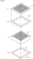
FIGS. 1 and 2 are perspective diagrams of an antenna module according to an embodiment of the present disclosure. -
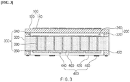
FIG. 3 is a cross-sectional diagram of an antenna module according to an embodiment of the present disclosure. -
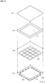
FIGS. 4 and5 are exploded perspective diagrams of an antenna module according to an embodiment of the present disclosure. -
FIG. 6 is a top diagram of a first base substrate illustrated inFIG. 1 . -
FIG. 7 is a top diagram of a first adhesive part illustrated inFIG. 1 . -
FIG. 8 is a top diagram of a second antenna part illustrated inFIG. 1 . -
FIG. 9 is a bottom diagram of the second antenna part illustrated inFIG, 1 . -
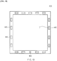
FIG. 10 is a top diagram of a second adhesive part illustrated inFIG. 1 . - Hereinafter, the most preferred embodiments of the present disclosure will be described in detail with reference to the accompanying drawings so that those skilled in the art to which the present disclosure pertains may easily carry out the technical spirit of the present disclosure. First, in adding reference numerals to the components of each drawing, it should be noted that the same components have the same reference numerals as much as possible even if they are displayed on different drawings. Further, in describing the present disclosure, when it is determined that the detailed description of the related well-known configuration or function may obscure the gist of the present disclosure, the detailed description thereof will be omitted.
- Referring to
FIGS. 1 to 5 , an antenna module according to an embodiment of the present disclosure is an antenna mounted in a base station or a portable terminal of a 5G communication system. - The antenna module is configured to include a
first antenna part 100, a firstadhesive part 200, asecond antenna part 300, and a secondadhesive part 400. Thefirst antenna part 100 is disposed on the uppermost portion of the antenna module. The firstadhesive part 200, thesecond antenna part 300, and the secondadhesive part 400 are sequentially stacked below thefirst antenna part 100. Accordingly, the antenna module is formed of an Antenna in Package (AiP) in which a plurality of radiation patterns are disposed on the uppermost portion thereof and a plurality ofchipsets 360 are disposed on the lowermost portion thereof. - The
first antenna part 100 and thesecond antenna part 300 are composed of a base substrate of a heterogeneous material. The radiation pattern is formed on the upper surface of thefirst antenna part 100 and the upper surface of thesecond antenna part 300, respectively. The plurality ofchipsets 360 are formed on the lower surface of thesecond antenna part 300. - The first
adhesive part 200 is interposed between thefirst antenna part 100 and thesecond antenna part 300. The firstadhesive part 200 adheres thefirst antenna part 100 and thesecond antenna part 300. The firstadhesive part 200 has is formed with a hole configured to accommodate the radiation pattern of thesecond antenna part 300. At this time, the hole formed in the firstadhesive part 200 forms an air gap between thefirst antenna part 100 and thesecond antenna part 300. The hole formed in the firstadhesive part 200 forms the air gap between the radiation pattern of thefirst antenna part 100 and the radiation pattern of thesecond antenna part 300. - The second
adhesive part 400 is adhered to the lower surface of thesecond antenna part 300. The secondadhesive part 400 is formed with a hole configured to accommodate the plurality ofchipsets 360 formed on the lower surface of thesecond antenna part 300. A plurality ofexternal terminal patterns 480 andinput terminals 460 are formed on the lower surface of the secondadhesive part 400. Theexternal terminal pattern 480 is a terminal configured to connect the antenna module with an external circuit. Theinput terminal 460 is a terminal configured to receive a signal from an external circuit. - The
first antenna part 100 includes afirst base substrate 120. Thefirst base substrate 120 is composed of a plate-shaped substrate. Thefirst base substrate 120 may be composed of a substrate such as a Rogers substrate, Flame Retardant Type 4 (FR-4), Teflon, Polyimide, or polyethylene, which is generally used for a circuit substrate. - The
first antenna part 100 further includes a plurality offirst radiation patterns 140. At this time, the plurality offirst radiation patterns 140 correspond to the radiation patterns disposed on the uppermost portion of the antenna module. - The plurality of
first radiation patterns 140 may be made of a metal material such as copper (Cu) or silver (Ag). The plurality offirst radiation patterns 140 are formed on the upper surface of thefirst base substrate 120 through a printing process. The plurality offirst radiation patterns 140 may be disposed in a matrix on the upper surface of thefirst base substrate 120. - Referring to
FIG. 6 , the plurality offirst radiation patterns 140 may be, for example, composed of 64 pieces and disposed in eight rows and eight columns on the upper surface of thefirst base substrate 120. Here, the number and matrix structure of thefirst radiation pattern 140 may be formed variously according to the characteristics and size of the antenna. - The first
adhesive part 200 is interposed between thefirst antenna part 100 and thesecond antenna part 300 to adhere thefirst antenna part 100 and thesecond antenna part 300. The upper surface of the firstadhesive part 200 is adhered to the lower surface of thefirst base substrate 120. The lower surface of the firstadhesive part 200 is adhered to the upper surface of thesecond base substrate 320. - To this end, the first
adhesive part 200 includes a firstadhesive substrate 220. The firstadhesive substrate 220 is composed of a plate-like dielectric. For example, the firstadhesive substrate 220 is a plate-shaped FR-4 substrate. - The first
adhesive part 200 forms an air gap between thefirst antenna part 100 and thesecond antenna part 300. - To this end, the first
adhesive part 200 further includes anair gap hole 240 formed by penetrating the firstadhesive substrate 220. Theair gap hole 240 forms an air gap between thefirst antenna part 100 and thesecond antenna part 300 as the firstadhesive part 200 is interposed between thefirst antenna part 100 and thesecond antenna part 300. - The
air gap hole 240 is disposed between the lower surface of thefirst base substrate 120 and the upper surface of thesecond base substrate 320. Theair gap hole 240 forms an air gap between the plurality offirst radiation patterns 140 and the plurality ofsecond radiation patterns 340. At this time, theair gap hole 240 accommodates the plurality ofsecond radiation patterns 340 formed on the upper surface of thesecond base substrate 320. - Referring to
FIG. 7 , the firstadhesive part 200 is formed in a frame (or donut) shape as theair gap hole 240 is formed in the firstadhesive substrate 220. The upper surface of the firstadhesive part 200 is adhered to the lower surface of thefirst base substrate 120. The upper surface of the firstadhesive part 200 is adhered along the outer circumference of the lower surface of thefirst base substrate 120. The lower surface of the firstadhesive part 200 is adhered to the upper surface of thesecond base substrate 320. The lower surface of the firstadhesive part 200 is adhered along the outer circumference of the upper surface of thesecond base substrate 320. - Meanwhile, the first
adhesive part 200 may include a plurality of air gap holes 240. The firstadhesive part 200 may be formed in a lattice structure in which the plurality of air gap holes 240 are formed in a multi-row and a multi-column. At this time, one or moresecond radiation patterns 340 may be accommodated in oneair gap hole 240. - As described above, it is possible for the antenna module to stack the
first antenna part 100 and thesecond antenna part 300 made of a heterogeneous material, thereby preventing breakdown of thefirst antenna part 100 and thesecond antenna part 300 during the manufacturing of the antenna module. - Further, it is possible for the antenna module to adhere the
first antenna part 100 and thesecond antenna part 300 by using the firstadhesive part 200 having theair gap hole 240 formed therein, thereby forming the air gap between the plurality offirst radiation patterns 140 formed on thefirst antenna part 100 and the plurality ofsecond radiation patterns 340 formed on thesecond antenna part 300 while preventing breakdown of thefirst antenna part 100 and thesecond antenna part 300 during the manufacturing of the antenna module. - Further, it is possible for the antenna module to form the air gap between the
first radiation pattern 140 and thesecond radiation pattern 340, thereby operating as an antenna that receives a frequency band signal such as 5th generation mobile communications (5G) or Wireless Gigabit Alliance (WiGig), which is a high frequency band. - Further, it is possible for the antenna module to form the air gap between the
first antenna part 100 and thesecond antenna part 300 made of a heterogeneous material, thereby implementing a high data transfer rate by increasing the propagation distance of the radio wave while the occurrence of breakdown during the manufacturing thereof and minimizing the path loss of the radio wave. - The
second antenna part 300 includes thesecond base substrate 320 adhered to the lower surface of the firstadhesive part 200. Thesecond base substrate 320 is made of a plate-shaped ceramic material. For example, thesecond base substrate 320 may be a Low Temperature Co-fired Ceramic (LTCC). Thesecond base substrate 320 may also be made of a ceramic material containing at least one among alumina (Al2O3), zirconium oxide (ZrO2), aluminum nitride (AlN), and silicon nitride (Si3N4). - The
second antenna part 300 further includes the plurality ofsecond radiation patterns 340 formed on the upper surface of thesecond base substrate 320. The plurality ofsecond radiation patterns 340 are made of a metal material such as copper (Cu) and silver (Ag). The plurality ofsecond radiation patterns 340 are formed on the upper surface of thesecond base substrate 320 through a printing process. The plurality ofsecond radiation patterns 340 may be disposed in a matrix on the upper surface of thesecond base substrate 320. - Referring to
FIG. 8 , the plurality ofsecond radiation patterns 340 may be, for example, composed of 64 pieces, and disposed in eight rows and eight columns on the upper surface of thesecond base substrate 320. Here, the number and matrix structure of thesecond radiation pattern 340 may be formed variously according to the characteristics and the size of the antenna. - The number and matrix structure of the
second radiation pattern 340 is preferably formed to be the same as thefirst radiation pattern 140. Of course, the number and matrix structure of thefirst radiation pattern 140 and thesecond radiation pattern 340 may also be formed variously according to the antenna characteristics. - The
second radiation pattern 340 is formed to overlap one of the plurality offirst radiation patterns 140 with theair gap hole 240 interposed therebetween. Here, the overlapping may be understood as thesecond radiation pattern 340 overlapping the entire surface of one of the plurality offirst radiation patterns 140. The overlapping may also be understood as thesecond radiation pattern 340 overlapping a portion of one of the plurality offirst radiation patterns 140. - As the plurality of
second radiation patterns 340 overlap the plurality offirst radiation patterns 140 with theair gap hole 240 interposed therebetween, thesecond radiation pattern 340 and thefirst radiation pattern 140 become a coupling. Here, the coupling means a state where it is electromagnetically coupled to each other in a state spaced apart from each other, rather than a state electrically, directly connected to each other. - The
second antenna part 300 further includes a plurality ofconnection patterns 380 formed in thesecond base substrate 320. - The plurality of
connection patterns 380 are made of a metal material such as copper (Cu) and silver (Ag). The plurality ofconnection patterns 380 connect thesecond radiation pattern 340 and thechipset 360 formed on the upper surface and the lower surface of thesecond base substrate 320, respectively. - The plurality of
connection patterns 380 processes signal transmission between thechipset 360 and thesecond radiation pattern 340. The plurality ofconnection patterns 380 transmit a signal received through thefirst radiation pattern 140 and thesecond radiation pattern 340 to thechipset 360. The plurality ofconnection patterns 380 may also transmit the signal input to thechipset 360 to thefirst radiation pattern 140 and thesecond radiation pattern 340. - The plurality of
connection patterns 380 may be composed of a via hole penetrating thesecond base substrate 320. The plurality ofconnection patterns 380 may be formed by plating a metal material such as copper or silver on the inner wall surface of the via hole. The plurality ofconnection patterns 380 may be formed by filling a metal material in the via hole. - Here, although it has been illustrated in
FIG. 3 that the plurality ofconnection patterns 380 vertically penetrate thesecond base substrate 320 to connect thesecond radiation pattern 340 and thechipset 360 in order to easily explain the antenna module according to an embodiment of the present disclosure, it is not limited thereto and may be formed in various forms. - Further, the
second base substrate 320 may be formed in a multi-layer structure in order to form the plurality ofconnection patterns 380. At this time, thesecond base substrate 320 may form a metal pattern on at least one surface of each layer, and form the plurality ofconnection patterns 380 by connecting metal patterns through the via hole formed in each layer. - The
second antenna part 300 further includes a plurality ofchipsets 360 formed on the lower surface of thesecond base substrate 320. The plurality ofchipsets 360 may be disposed in a matrix on the lower surface of thesecond base substrate 320. The plurality ofsecond radiation patterns 340 are connected to onechipset 360 through theconnection pattern 380. - Referring to
FIG. 9 , if there are 64second radiation patterns 340 and foursecond radiation patterns 340 are connected to onechipset 360, the plurality ofchipsets 360 may be composed of 16 pieces and disposed in four rows and four columns on the lower surface of thesecond base substrate 320. Here, the number and matrix structure of thechipset 360 may be formed variously according to the number and processing capacity of thesecond radiation pattern 340 to be connected. - The second
adhesive part 400 is disposed at the lowermost portion of the antenna module. The secondadhesive part 400 accommodates thechipset 360 formed below thesecond antenna part 300. The externalterminal pattern 480 for connecting with an external circuit substrate is formed below the secondadhesive part 400. Theinput terminal 460 configured to receive a signal from the external circuit substrate may be formed below the secondadhesive part 400. - The second
adhesive part 400 is adhered to the lower surface of thesecond antenna part 300. The upper surface of the secondadhesive part 400 is adhered to the lower surface of thesecond antenna part 300. To this end, the secondadhesive part 400 includes a secondadhesive substrate 420. The secondadhesive substrate 420 is composed of a plate-shaped dielectric. For example, the secondadhesive substrate 420 is a plate-shaped FR-4 substrate. - The second
adhesive part 400 further includes anaccommodation hole 440 formed by penetrating the secondadhesive substrate 420. Theaccommodation hole 440 accommodates the plurality ofchipsets 360 formed on the lower surface of thesecond antenna part 300 as the secondadhesive part 400 is adhered to the lower surface of thesecond antenna part 300. At this time, the thickness of theaccommodation hole 440 may be formed thicker than the thickness of thechipset 360. - Referring to
FIG. 10 , the secondadhesive part 400 is formed in a frame (or donut) shape as theaccommodation hole 440 is formed in the secondadhesive substrate 420. The upper surface of the secondadhesive part 400 is adhered to the lower surface of thesecond base substrate 320. The upper surface of the secondadhesive part 400 is adhered along the outer circumference of the lower surface of thesecond base substrate 320. The lower surface of the secondadhesive part 400 is adhered to the upper surface of the circuit substrate on which the antenna module is mounted. - At this time, the second
adhesive part 400 further includes a plurality of externalterminal patterns 480 configured to connect the antenna module with the circuit substrate. - The plurality of external
terminal patterns 480 may be made of a metal material such as copper or silver. The plurality of externalterminal patterns 480 are formed on the lower surface of the secondadhesive substrate 420 through a printing process. The plurality of externalterminal patterns 480 may be disposed to be spaced apart from each other on the lower surface of the secondadhesive substrate 420. The plurality of externalterminal patterns 480 may be connected with thechipset 360 through the patterns formed on the secondadhesive substrate 420 and thesecond base substrate 320. - The plurality of external
terminal patterns 480 are electrically connected directly to the terminal of the circuit substrate as the antenna module is mounted on the circuit substrate. The plurality of externalterminal patterns 480 may also be connected to the circuit substrate through a cable or a connection circuit substrate. - The second
adhesive part 400 may further include theinput terminal 460 configured to receive an external signal. Theinput terminal 460 receives the external signal to transmit it to thechipset 360. To this end, theinput terminal 460 may be connected with thechipset 360 through the patterns formed on the secondadhesive substrate 420 and thesecond base substrate 320. - As described above, although preferred embodiments according to the present disclosure has been described, it may be modified in various forms, and it is understood by those skilled in the art that various modified examples and changed examples may be practiced without departing from the claims of the present disclosure.
Claims (20)
- An antenna module, comprising:a first base substrate;a plurality of first radiation patterns formed on the upper surface of the first base substrate;a second base substrate disposed below the first base substrate;a plurality of second radiation patterns formed on the upper surface of the second base substrate;a plurality of chipsets disposed on the lower surface of the second base substrate; anda first adhesive substrate interposed between the first base substrate and the second base substrate,wherein the first adhesive substrate is formed with an air gap hole having the plurality of second radiation patterns accommodated therein, andwherein the air gap hole forms an air gap between the plurality of first radiation patterns and the plurality of second radiation patterns.
- The antenna module of claim 1,
wherein the first adhesive substrate is formed in a frame, and
wherein the upper surface of the first adhesive substrate is disposed along the outer circumference of the lower surface of the first base substrate, and the lower surface of the first adhesive substrate is disposed along the outer circumference of the upper surface of the second base substrate. - The antenna module of claim 1,
wherein the plurality of second radiation patterns overlap one first radiation pattern with the air gap hole interposed therebetween, respectively. - The antenna module of claim 1,
wherein the air gap hole accommodates the plurality of second radiation patterns. - The antenna module of claim 1,
wherein the first adhesive substrate is formed in a lattice structure in which a plurality of air gap holes are disposed in a matrix. - The antenna module of claim 5,
wherein the plurality of air gap holes accommodate one or more second radiation patterns, respectively. - The antenna module of claim 1,
wherein the air gap hole forms an air gap between the lower surface of the first base substrate and the upper surface of the second base substrate. - The antenna module of claim 1,
wherein the plurality of first radiation patterns are disposed in a matrix on the upper surface of the first base substrate, and the plurality of second radiation patterns are disposed in a matrix on the upper surface of the second base substrate. - The antenna module of claim 1,
wherein the plurality of chipsets are disposed in a matrix on the lower surface of the second base substrate. - The antenna module of claim 1,
wherein at least one among the plurality of chipsets is connected with two or more second radiation patterns. - The antenna module of claim 1, further comprising a plurality of connection patterns formed on the second base substrate,
wherein the plurality of connection patterns connect the plurality of second radiation patterns with the plurality of chipsets. - The antenna module of claim 1, further comprising a second adhesive substrate disposed on the lower surface of the second base substrate.
- The antenna module of claim 12,
wherein the second adhesive substrate is formed with an accommodation hole that accommodates the plurality of chipsets. - The antenna module of claim 12,
wherein the second adhesive substrate is formed with a plurality of accommodation holes, and
wherein the plurality of accommodation holes accommodate one or more chipsets, respectively. - The antenna module of claim 12,
wherein the thickness of the second adhesive substrate is formed thicker than the thickness of the plurality of chipsets. - The antenna module of claim 12,
wherein the second adhesive substrate is formed in a frame shape and disposed on the lower surface of the second base substrate, and disposed along the outer circumference of the lower surface of the second base substrate. - The antenna module of claim 12, further comprising an external terminal pattern formed on the lower surface of the second adhesive substrate.
- The antenna module of claim 12, further comprising an input terminal formed on the lower surface of the second adhesive substrate.
- The antenna module of claim 1,
wherein the second base substrate is a plated-shaped Low Temperature Co-fired Ceramic material. - The antenna module of claim 19,
wherein the first base substrate is made of a different material from that of the second base substrate.
Applications Claiming Priority (2)
| Application Number | Priority Date | Filing Date | Title |
|---|---|---|---|
| KR20170056429 | 2017-05-02 | ||
| PCT/KR2018/005014 WO2018203640A1 (en) | 2017-05-02 | 2018-04-30 | Antenna module |
Publications (3)
| Publication Number | Publication Date |
|---|---|
| EP3621153A1 true EP3621153A1 (en) | 2020-03-11 |
| EP3621153A4 EP3621153A4 (en) | 2021-01-20 |
| EP3621153B1 EP3621153B1 (en) | 2022-11-09 |
Family
ID=64016897
Family Applications (1)
| Application Number | Title | Priority Date | Filing Date |
|---|---|---|---|
| EP18794886.4A Active EP3621153B1 (en) | 2017-05-02 | 2018-04-30 | Antenna module |
Country Status (6)
| Country | Link |
|---|---|
| US (1) | US11251538B2 (en) |
| EP (1) | EP3621153B1 (en) |
| JP (1) | JP7053669B2 (en) |
| KR (1) | KR102020676B1 (en) |
| CN (1) | CN110731032B (en) |
| WO (1) | WO2018203640A1 (en) |
Families Citing this family (10)
| Publication number | Priority date | Publication date | Assignee | Title |
|---|---|---|---|---|
| TW201110888A (en) * | 2009-09-24 | 2011-04-01 | Yuka Sangyo Co Ltd | Livestock feed composition and method of feeding livestock therewith |
| KR102552854B1 (en) * | 2018-11-22 | 2023-07-06 | 엘에스엠트론 주식회사 | Array Patch Antenna Module Using Coupling Feeding |
| US11664872B2 (en) | 2019-01-31 | 2023-05-30 | Spreadtrum Communications (Shanghai) Co., Ltd. | Beam detection method and device, beam adjusting method and device, antenna module selection method and device, and computer readable storage media |
| CN111294093B (en) * | 2019-01-31 | 2022-03-22 | 展讯通信(上海)有限公司 | Beam detection method and device based on AiP structure, and computer-readable storage medium |
| US12212064B2 (en) * | 2020-10-27 | 2025-01-28 | Mixcomm, Inc. | Methods and apparatus for implementing antenna assemblies and/or combining antenna assemblies to form arrays |
| US20240063533A1 (en) * | 2020-12-28 | 2024-02-22 | AMOSENSE Co.,Ltd | Method for manufacturing antenna module ceramic substrate |
| JP7621165B2 (en) * | 2021-04-05 | 2025-01-24 | 日本特殊陶業株式会社 | Antenna Board |
| WO2023068660A1 (en) | 2021-10-19 | 2023-04-27 | 삼성전자 주식회사 | Antenna assembly and electronic device comprising same |
| KR20240088482A (en) * | 2022-12-13 | 2024-06-20 | 엘지이노텍 주식회사 | AiP(Antenna in Package) module |
| WO2026023101A1 (en) * | 2024-07-24 | 2026-01-29 | 三菱電機株式会社 | Array antenna device |
Family Cites Families (30)
| Publication number | Priority date | Publication date | Assignee | Title |
|---|---|---|---|---|
| JP3683422B2 (en) | 1998-10-30 | 2005-08-17 | 三菱電機株式会社 | Microstrip antenna and microstrip antenna substrate |
| US6624787B2 (en) * | 2001-10-01 | 2003-09-23 | Raytheon Company | Slot coupled, polarized, egg-crate radiator |
| JP2004327641A (en) * | 2003-04-24 | 2004-11-18 | Tdk Corp | Electronic component module |
| JP2005086603A (en) * | 2003-09-10 | 2005-03-31 | Tdk Corp | Electronic component module and manufacturing method thereof |
| US7183622B2 (en) * | 2004-06-30 | 2007-02-27 | Intel Corporation | Module integrating MEMS and passive components |
| DE102004046633A1 (en) * | 2004-09-25 | 2006-03-30 | Robert Bosch Gmbh | Carrier arrangement for a radio-frequency antenna and method for its production |
| US8279131B2 (en) * | 2006-09-21 | 2012-10-02 | Raytheon Company | Panel array |
| US8525729B1 (en) * | 2009-01-09 | 2013-09-03 | Lockheed Martin Corporation | Antenna tiles with ground cavities integrated into support structure |
| US8072384B2 (en) * | 2009-01-14 | 2011-12-06 | Laird Technologies, Inc. | Dual-polarized antenna modules |
| DE102010006809A1 (en) * | 2010-02-04 | 2011-08-04 | EADS Deutschland GmbH, 85521 | Stacked microstrip antenna |
| JP2012235351A (en) * | 2011-05-02 | 2012-11-29 | Denso Corp | Antenna device |
| US8860532B2 (en) * | 2011-05-20 | 2014-10-14 | University Of Central Florida Research Foundation, Inc. | Integrated cavity filter/antenna system |
| KR101780024B1 (en) | 2011-10-19 | 2017-09-20 | 삼성전자주식회사 | Antenna-Printed Circuit Board package |
| WO2014020787A1 (en) | 2012-08-03 | 2014-02-06 | パナソニック株式会社 | Electronic component module and mounting body therefor |
| US9196951B2 (en) * | 2012-11-26 | 2015-11-24 | International Business Machines Corporation | Millimeter-wave radio frequency integrated circuit packages with integrated antennas |
| KR101540607B1 (en) * | 2013-07-26 | 2015-07-31 | (주)파트론 | Base attached antenna and attaching layer |
| US9634641B2 (en) * | 2013-11-06 | 2017-04-25 | Taiyo Yuden Co., Ltd. | Electronic module having an interconnection substrate with a buried electronic device therein |
| JP6335476B2 (en) * | 2013-11-06 | 2018-05-30 | 太陽誘電株式会社 | module |
| KR102305113B1 (en) | 2014-04-07 | 2021-09-28 | 삼성전자주식회사 | Assist device for electronic device with antenna |
| US10658758B2 (en) * | 2014-04-17 | 2020-05-19 | The Boeing Company | Modular antenna assembly |
| KR102185196B1 (en) * | 2014-07-04 | 2020-12-01 | 삼성전자주식회사 | Apparatus for antenna in wireless communication device |
| US9620464B2 (en) * | 2014-08-13 | 2017-04-11 | International Business Machines Corporation | Wireless communications package with integrated antennas and air cavity |
| JP6299878B2 (en) * | 2014-10-07 | 2018-03-28 | 株式会社村田製作所 | High frequency communication module and high frequency communication device |
| WO2016067906A1 (en) * | 2014-10-30 | 2016-05-06 | 三菱電機株式会社 | Array antenna device and method for manufacturing same |
| DE102015202801A1 (en) | 2015-02-17 | 2016-08-18 | Robert Bosch Gmbh | Antenna arrangement and method for producing an antenna arrangement |
| US10892547B2 (en) * | 2015-07-07 | 2021-01-12 | Cohere Technologies, Inc. | Inconspicuous multi-directional antenna system configured for multiple polarization modes |
| JP6591909B2 (en) | 2015-07-27 | 2019-10-16 | 京セラ株式会社 | Antenna module |
| CN105609944B (en) * | 2015-12-28 | 2018-06-05 | 西安电子科技大学昆山创新研究院 | Double-deck fractal microstrip radio frequency package antenna based on cavity structure |
| CN109983619B (en) * | 2016-12-20 | 2020-09-01 | 京瓷株式会社 | Antenna module |
| US10854978B2 (en) * | 2018-04-23 | 2020-12-01 | Samsung Electro-Mechanics Co., Ltd. | Antenna apparatus and antenna module |
-
2018
- 2018-04-30 EP EP18794886.4A patent/EP3621153B1/en active Active
- 2018-04-30 CN CN201880036825.5A patent/CN110731032B/en active Active
- 2018-04-30 KR KR1020180049871A patent/KR102020676B1/en active Active
- 2018-04-30 JP JP2019559764A patent/JP7053669B2/en active Active
- 2018-04-30 US US16/610,048 patent/US11251538B2/en active Active
- 2018-04-30 WO PCT/KR2018/005014 patent/WO2018203640A1/en not_active Ceased
Also Published As
| Publication number | Publication date |
|---|---|
| JP2020521356A (en) | 2020-07-16 |
| KR20180122286A (en) | 2018-11-12 |
| CN110731032A (en) | 2020-01-24 |
| WO2018203640A1 (en) | 2018-11-08 |
| JP7053669B2 (en) | 2022-04-12 |
| US11251538B2 (en) | 2022-02-15 |
| EP3621153A4 (en) | 2021-01-20 |
| CN110731032B (en) | 2021-10-29 |
| EP3621153B1 (en) | 2022-11-09 |
| US20210305719A1 (en) | 2021-09-30 |
| KR102020676B1 (en) | 2019-09-11 |
Similar Documents
| Publication | Publication Date | Title |
|---|---|---|
| US11251538B2 (en) | Antenna module | |
| US11831084B2 (en) | Dual-polarized antenna, antenna array, and communications device | |
| US10044111B2 (en) | Wideband dual-polarized patch antenna | |
| US10056922B1 (en) | Radio frequency device modules and methods of formation thereof | |
| US10771101B2 (en) | Devices and methods related to packaging of radio-frequency devices on ceramic substrates | |
| US11575194B2 (en) | Antenna structure and antenna array | |
| US20100033393A1 (en) | Techniques for Mounting a Millimeter Wave Antenna and a Radio Frequency Integrated Circuit Onto a PCB | |
| EP3465823B1 (en) | C-fed antenna formed on multi-layer printed circuit board edge | |
| CN111029739B (en) | Antenna unit and electronic equipment | |
| EP3780269B1 (en) | Packaging structure | |
| CN115810906A (en) | Electronic device with compact ultra-wideband antenna module | |
| EP3455907B1 (en) | C-fed antenna formed on multi-layer printed circuit board edge | |
| US20200412008A1 (en) | Antenna device and low-profile antenna | |
| CN109449608B (en) | Microstrip array antenna structure capable of improving isolation degree between antennas | |
| CN110098474A (en) | A kind of antenna modules and terminal device | |
| JP6987999B2 (en) | Cavity structure antenna package | |
| CN219286667U (en) | Dual-frequency dielectric resonant antenna and communication equipment | |
| CN110829021A (en) | An antenna unit and electronic equipment | |
| EP3751666B1 (en) | Multi-band, dual-polarization antenna array | |
| CN110808454A (en) | An antenna unit and electronic equipment | |
| US10505276B2 (en) | Wireless communications assembly with integrated active phased-array antenna | |
| US20200076471A1 (en) | High bandwidth scalable wireless near-field interface | |
| US20240204419A1 (en) | Contention-based access with spatial re-use | |
| CN110011028A (en) | A kind of antenna system, communicating terminal and base station | |
| WO2019113112A1 (en) | High bandwidth scalable wireless near-field interface |
Legal Events
| Date | Code | Title | Description |
|---|---|---|---|
| STAA | Information on the status of an ep patent application or granted ep patent |
Free format text: STATUS: THE INTERNATIONAL PUBLICATION HAS BEEN MADE |
|
| PUAI | Public reference made under article 153(3) epc to a published international application that has entered the european phase |
Free format text: ORIGINAL CODE: 0009012 |
|
| STAA | Information on the status of an ep patent application or granted ep patent |
Free format text: STATUS: REQUEST FOR EXAMINATION WAS MADE |
|
| 17P | Request for examination filed |
Effective date: 20191030 |
|
| AK | Designated contracting states |
Kind code of ref document: A1 Designated state(s): AL AT BE BG CH CY CZ DE DK EE ES FI FR GB GR HR HU IE IS IT LI LT LU LV MC MK MT NL NO PL PT RO RS SE SI SK SM TR |
|
| AX | Request for extension of the european patent |
Extension state: BA ME |
|
| DAV | Request for validation of the european patent (deleted) | ||
| DAX | Request for extension of the european patent (deleted) | ||
| A4 | Supplementary search report drawn up and despatched |
Effective date: 20201217 |
|
| RIC1 | Information provided on ipc code assigned before grant |
Ipc: H01Q 21/00 20060101ALI20201211BHEP Ipc: H01Q 1/22 20060101ALI20201211BHEP Ipc: H01Q 9/04 20060101ALI20201211BHEP Ipc: H01Q 5/25 20150101ALI20201211BHEP Ipc: H01Q 1/38 20060101AFI20201211BHEP Ipc: H01Q 21/06 20060101ALI20201211BHEP |
|
| GRAP | Despatch of communication of intention to grant a patent |
Free format text: ORIGINAL CODE: EPIDOSNIGR1 |
|
| STAA | Information on the status of an ep patent application or granted ep patent |
Free format text: STATUS: GRANT OF PATENT IS INTENDED |
|
| INTG | Intention to grant announced |
Effective date: 20220524 |
|
| GRAS | Grant fee paid |
Free format text: ORIGINAL CODE: EPIDOSNIGR3 |
|
| GRAA | (expected) grant |
Free format text: ORIGINAL CODE: 0009210 |
|
| STAA | Information on the status of an ep patent application or granted ep patent |
Free format text: STATUS: THE PATENT HAS BEEN GRANTED |
|
| AK | Designated contracting states |
Kind code of ref document: B1 Designated state(s): AL AT BE BG CH CY CZ DE DK EE ES FI FR GB GR HR HU IE IS IT LI LT LU LV MC MK MT NL NO PL PT RO RS SE SI SK SM TR |
|
| REG | Reference to a national code |
Ref country code: GB Ref legal event code: FG4D |
|
| REG | Reference to a national code |
Ref country code: CH Ref legal event code: EP Ref country code: AT Ref legal event code: REF Ref document number: 1530968 Country of ref document: AT Kind code of ref document: T Effective date: 20221115 |
|
| REG | Reference to a national code |
Ref country code: DE Ref legal event code: R096 Ref document number: 602018042916 Country of ref document: DE |
|
| REG | Reference to a national code |
Ref country code: IE Ref legal event code: FG4D |
|
| REG | Reference to a national code |
Ref country code: LT Ref legal event code: MG9D |
|
| REG | Reference to a national code |
Ref country code: NL Ref legal event code: MP Effective date: 20221109 |
|
| REG | Reference to a national code |
Ref country code: AT Ref legal event code: MK05 Ref document number: 1530968 Country of ref document: AT Kind code of ref document: T Effective date: 20221109 |
|
| PG25 | Lapsed in a contracting state [announced via postgrant information from national office to epo] |
Ref country code: SE Free format text: LAPSE BECAUSE OF FAILURE TO SUBMIT A TRANSLATION OF THE DESCRIPTION OR TO PAY THE FEE WITHIN THE PRESCRIBED TIME-LIMIT Effective date: 20221109 Ref country code: PT Free format text: LAPSE BECAUSE OF FAILURE TO SUBMIT A TRANSLATION OF THE DESCRIPTION OR TO PAY THE FEE WITHIN THE PRESCRIBED TIME-LIMIT Effective date: 20230309 Ref country code: NO Free format text: LAPSE BECAUSE OF FAILURE TO SUBMIT A TRANSLATION OF THE DESCRIPTION OR TO PAY THE FEE WITHIN THE PRESCRIBED TIME-LIMIT Effective date: 20230209 Ref country code: LT Free format text: LAPSE BECAUSE OF FAILURE TO SUBMIT A TRANSLATION OF THE DESCRIPTION OR TO PAY THE FEE WITHIN THE PRESCRIBED TIME-LIMIT Effective date: 20221109 Ref country code: FI Free format text: LAPSE BECAUSE OF FAILURE TO SUBMIT A TRANSLATION OF THE DESCRIPTION OR TO PAY THE FEE WITHIN THE PRESCRIBED TIME-LIMIT Effective date: 20221109 Ref country code: ES Free format text: LAPSE BECAUSE OF FAILURE TO SUBMIT A TRANSLATION OF THE DESCRIPTION OR TO PAY THE FEE WITHIN THE PRESCRIBED TIME-LIMIT Effective date: 20221109 Ref country code: AT Free format text: LAPSE BECAUSE OF FAILURE TO SUBMIT A TRANSLATION OF THE DESCRIPTION OR TO PAY THE FEE WITHIN THE PRESCRIBED TIME-LIMIT Effective date: 20221109 |
|
| PG25 | Lapsed in a contracting state [announced via postgrant information from national office to epo] |
Ref country code: RS Free format text: LAPSE BECAUSE OF FAILURE TO SUBMIT A TRANSLATION OF THE DESCRIPTION OR TO PAY THE FEE WITHIN THE PRESCRIBED TIME-LIMIT Effective date: 20221109 Ref country code: PL Free format text: LAPSE BECAUSE OF FAILURE TO SUBMIT A TRANSLATION OF THE DESCRIPTION OR TO PAY THE FEE WITHIN THE PRESCRIBED TIME-LIMIT Effective date: 20221109 Ref country code: LV Free format text: LAPSE BECAUSE OF FAILURE TO SUBMIT A TRANSLATION OF THE DESCRIPTION OR TO PAY THE FEE WITHIN THE PRESCRIBED TIME-LIMIT Effective date: 20221109 Ref country code: IS Free format text: LAPSE BECAUSE OF FAILURE TO SUBMIT A TRANSLATION OF THE DESCRIPTION OR TO PAY THE FEE WITHIN THE PRESCRIBED TIME-LIMIT Effective date: 20230309 Ref country code: HR Free format text: LAPSE BECAUSE OF FAILURE TO SUBMIT A TRANSLATION OF THE DESCRIPTION OR TO PAY THE FEE WITHIN THE PRESCRIBED TIME-LIMIT Effective date: 20221109 Ref country code: GR Free format text: LAPSE BECAUSE OF FAILURE TO SUBMIT A TRANSLATION OF THE DESCRIPTION OR TO PAY THE FEE WITHIN THE PRESCRIBED TIME-LIMIT Effective date: 20230210 |
|
| PG25 | Lapsed in a contracting state [announced via postgrant information from national office to epo] |
Ref country code: NL Free format text: LAPSE BECAUSE OF FAILURE TO SUBMIT A TRANSLATION OF THE DESCRIPTION OR TO PAY THE FEE WITHIN THE PRESCRIBED TIME-LIMIT Effective date: 20221109 |
|
| PG25 | Lapsed in a contracting state [announced via postgrant information from national office to epo] |
Ref country code: SM Free format text: LAPSE BECAUSE OF FAILURE TO SUBMIT A TRANSLATION OF THE DESCRIPTION OR TO PAY THE FEE WITHIN THE PRESCRIBED TIME-LIMIT Effective date: 20221109 Ref country code: RO Free format text: LAPSE BECAUSE OF FAILURE TO SUBMIT A TRANSLATION OF THE DESCRIPTION OR TO PAY THE FEE WITHIN THE PRESCRIBED TIME-LIMIT Effective date: 20221109 Ref country code: EE Free format text: LAPSE BECAUSE OF FAILURE TO SUBMIT A TRANSLATION OF THE DESCRIPTION OR TO PAY THE FEE WITHIN THE PRESCRIBED TIME-LIMIT Effective date: 20221109 Ref country code: DK Free format text: LAPSE BECAUSE OF FAILURE TO SUBMIT A TRANSLATION OF THE DESCRIPTION OR TO PAY THE FEE WITHIN THE PRESCRIBED TIME-LIMIT Effective date: 20221109 Ref country code: CZ Free format text: LAPSE BECAUSE OF FAILURE TO SUBMIT A TRANSLATION OF THE DESCRIPTION OR TO PAY THE FEE WITHIN THE PRESCRIBED TIME-LIMIT Effective date: 20221109 |
|
| REG | Reference to a national code |
Ref country code: DE Ref legal event code: R097 Ref document number: 602018042916 Country of ref document: DE |
|
| PG25 | Lapsed in a contracting state [announced via postgrant information from national office to epo] |
Ref country code: SK Free format text: LAPSE BECAUSE OF FAILURE TO SUBMIT A TRANSLATION OF THE DESCRIPTION OR TO PAY THE FEE WITHIN THE PRESCRIBED TIME-LIMIT Effective date: 20221109 Ref country code: AL Free format text: LAPSE BECAUSE OF FAILURE TO SUBMIT A TRANSLATION OF THE DESCRIPTION OR TO PAY THE FEE WITHIN THE PRESCRIBED TIME-LIMIT Effective date: 20221109 |
|
| PLBE | No opposition filed within time limit |
Free format text: ORIGINAL CODE: 0009261 |
|
| STAA | Information on the status of an ep patent application or granted ep patent |
Free format text: STATUS: NO OPPOSITION FILED WITHIN TIME LIMIT |
|
| 26N | No opposition filed |
Effective date: 20230810 |
|
| PG25 | Lapsed in a contracting state [announced via postgrant information from national office to epo] |
Ref country code: SI Free format text: LAPSE BECAUSE OF FAILURE TO SUBMIT A TRANSLATION OF THE DESCRIPTION OR TO PAY THE FEE WITHIN THE PRESCRIBED TIME-LIMIT Effective date: 20221109 |
|
| REG | Reference to a national code |
Ref country code: CH Ref legal event code: PL |
|
| PG25 | Lapsed in a contracting state [announced via postgrant information from national office to epo] |
Ref country code: LU Free format text: LAPSE BECAUSE OF NON-PAYMENT OF DUE FEES Effective date: 20230430 |
|
| REG | Reference to a national code |
Ref country code: BE Ref legal event code: MM Effective date: 20230430 |
|
| PG25 | Lapsed in a contracting state [announced via postgrant information from national office to epo] |
Ref country code: MC Free format text: LAPSE BECAUSE OF FAILURE TO SUBMIT A TRANSLATION OF THE DESCRIPTION OR TO PAY THE FEE WITHIN THE PRESCRIBED TIME-LIMIT Effective date: 20221109 |
|
| PG25 | Lapsed in a contracting state [announced via postgrant information from national office to epo] |
Ref country code: MC Free format text: LAPSE BECAUSE OF FAILURE TO SUBMIT A TRANSLATION OF THE DESCRIPTION OR TO PAY THE FEE WITHIN THE PRESCRIBED TIME-LIMIT Effective date: 20221109 Ref country code: LI Free format text: LAPSE BECAUSE OF NON-PAYMENT OF DUE FEES Effective date: 20230430 Ref country code: CH Free format text: LAPSE BECAUSE OF NON-PAYMENT OF DUE FEES Effective date: 20230430 |
|
| REG | Reference to a national code |
Ref country code: IE Ref legal event code: MM4A |
|
| PG25 | Lapsed in a contracting state [announced via postgrant information from national office to epo] |
Ref country code: BE Free format text: LAPSE BECAUSE OF NON-PAYMENT OF DUE FEES Effective date: 20230430 |
|
| PG25 | Lapsed in a contracting state [announced via postgrant information from national office to epo] |
Ref country code: IE Free format text: LAPSE BECAUSE OF NON-PAYMENT OF DUE FEES Effective date: 20230430 |
|
| PG25 | Lapsed in a contracting state [announced via postgrant information from national office to epo] |
Ref country code: IE Free format text: LAPSE BECAUSE OF NON-PAYMENT OF DUE FEES Effective date: 20230430 |
|
| PG25 | Lapsed in a contracting state [announced via postgrant information from national office to epo] |
Ref country code: IT Free format text: LAPSE BECAUSE OF FAILURE TO SUBMIT A TRANSLATION OF THE DESCRIPTION OR TO PAY THE FEE WITHIN THE PRESCRIBED TIME-LIMIT Effective date: 20221109 |
|
| PG25 | Lapsed in a contracting state [announced via postgrant information from national office to epo] |
Ref country code: BG Free format text: LAPSE BECAUSE OF FAILURE TO SUBMIT A TRANSLATION OF THE DESCRIPTION OR TO PAY THE FEE WITHIN THE PRESCRIBED TIME-LIMIT Effective date: 20221109 |
|
| PG25 | Lapsed in a contracting state [announced via postgrant information from national office to epo] |
Ref country code: BG Free format text: LAPSE BECAUSE OF FAILURE TO SUBMIT A TRANSLATION OF THE DESCRIPTION OR TO PAY THE FEE WITHIN THE PRESCRIBED TIME-LIMIT Effective date: 20221109 |
|
| PGFP | Annual fee paid to national office [announced via postgrant information from national office to epo] |
Ref country code: DE Payment date: 20250320 Year of fee payment: 8 |
|
| PG25 | Lapsed in a contracting state [announced via postgrant information from national office to epo] |
Ref country code: CY Free format text: LAPSE BECAUSE OF FAILURE TO SUBMIT A TRANSLATION OF THE DESCRIPTION OR TO PAY THE FEE WITHIN THE PRESCRIBED TIME-LIMIT; INVALID AB INITIO Effective date: 20180430 |
|
| PG25 | Lapsed in a contracting state [announced via postgrant information from national office to epo] |
Ref country code: HU Free format text: LAPSE BECAUSE OF FAILURE TO SUBMIT A TRANSLATION OF THE DESCRIPTION OR TO PAY THE FEE WITHIN THE PRESCRIBED TIME-LIMIT; INVALID AB INITIO Effective date: 20180430 |
|
| PG25 | Lapsed in a contracting state [announced via postgrant information from national office to epo] |
Ref country code: TR Free format text: LAPSE BECAUSE OF FAILURE TO SUBMIT A TRANSLATION OF THE DESCRIPTION OR TO PAY THE FEE WITHIN THE PRESCRIBED TIME-LIMIT Effective date: 20221109 |
|
| PGFP | Annual fee paid to national office [announced via postgrant information from national office to epo] |
Ref country code: GB Payment date: 20260324 Year of fee payment: 9 |
|
| PGFP | Annual fee paid to national office [announced via postgrant information from national office to epo] |
Ref country code: FR Payment date: 20260323 Year of fee payment: 9 |