EP3621126A1 - Manufacturing of an integrated electronic circuit which includes a component based on metal ion migration and reduction - Google Patents
Manufacturing of an integrated electronic circuit which includes a component based on metal ion migration and reduction Download PDFInfo
- Publication number
- EP3621126A1 EP3621126A1 EP18306168.8A EP18306168A EP3621126A1 EP 3621126 A1 EP3621126 A1 EP 3621126A1 EP 18306168 A EP18306168 A EP 18306168A EP 3621126 A1 EP3621126 A1 EP 3621126A1
- Authority
- EP
- European Patent Office
- Prior art keywords
- container
- metal
- layer
- electrode
- atoms
- Prior art date
- Legal status (The legal status is an assumption and is not a legal conclusion. Google has not performed a legal analysis and makes no representation as to the accuracy of the status listed.)
- Granted
Links
Images

Classifications
-
- H—ELECTRICITY
- H10—SEMICONDUCTOR DEVICES; ELECTRIC SOLID-STATE DEVICES NOT OTHERWISE PROVIDED FOR
- H10N—ELECTRIC SOLID-STATE DEVICES NOT OTHERWISE PROVIDED FOR
- H10N70/00—Solid-state devices having no potential barriers, and specially adapted for rectifying, amplifying, oscillating or switching
- H10N70/20—Multistable switching devices, e.g. memristors
- H10N70/24—Multistable switching devices, e.g. memristors based on migration or redistribution of ionic species, e.g. anions, vacancies
- H10N70/245—Multistable switching devices, e.g. memristors based on migration or redistribution of ionic species, e.g. anions, vacancies the species being metal cations, e.g. programmable metallization cells
-
- H—ELECTRICITY
- H10—SEMICONDUCTOR DEVICES; ELECTRIC SOLID-STATE DEVICES NOT OTHERWISE PROVIDED FOR
- H10B—ELECTRONIC MEMORY DEVICES
- H10B63/00—Resistance change memory devices, e.g. resistive RAM [ReRAM] devices
- H10B63/80—Arrangements comprising multiple bistable or multi-stable switching components of the same type on a plane parallel to the substrate, e.g. cross-point arrays
- H10B63/84—Arrangements comprising multiple bistable or multi-stable switching components of the same type on a plane parallel to the substrate, e.g. cross-point arrays arranged in a direction perpendicular to the substrate, e.g. 3D cell arrays
- H10B63/845—Arrangements comprising multiple bistable or multi-stable switching components of the same type on a plane parallel to the substrate, e.g. cross-point arrays arranged in a direction perpendicular to the substrate, e.g. 3D cell arrays the switching components being connected to a common vertical conductor
-
- C—CHEMISTRY; METALLURGY
- C23—COATING METALLIC MATERIAL; COATING MATERIAL WITH METALLIC MATERIAL; CHEMICAL SURFACE TREATMENT; DIFFUSION TREATMENT OF METALLIC MATERIAL; COATING BY VACUUM EVAPORATION, BY SPUTTERING, BY ION IMPLANTATION OR BY CHEMICAL VAPOUR DEPOSITION, IN GENERAL; INHIBITING CORROSION OF METALLIC MATERIAL OR INCRUSTATION IN GENERAL
- C23C—COATING METALLIC MATERIAL; COATING MATERIAL WITH METALLIC MATERIAL; SURFACE TREATMENT OF METALLIC MATERIAL BY DIFFUSION INTO THE SURFACE, BY CHEMICAL CONVERSION OR SUBSTITUTION; COATING BY VACUUM EVAPORATION, BY SPUTTERING, BY ION IMPLANTATION OR BY CHEMICAL VAPOUR DEPOSITION, IN GENERAL
- C23C16/00—Chemical coating by decomposition of gaseous compounds, without leaving reaction products of surface material in the coating, i.e. chemical vapour deposition [CVD] processes
- C23C16/04—Coating on selected surface areas, e.g. using masks
- C23C16/045—Coating cavities or hollow spaces, e.g. interior of tubes; Infiltration of porous substrates
-
- C—CHEMISTRY; METALLURGY
- C23—COATING METALLIC MATERIAL; COATING MATERIAL WITH METALLIC MATERIAL; CHEMICAL SURFACE TREATMENT; DIFFUSION TREATMENT OF METALLIC MATERIAL; COATING BY VACUUM EVAPORATION, BY SPUTTERING, BY ION IMPLANTATION OR BY CHEMICAL VAPOUR DEPOSITION, IN GENERAL; INHIBITING CORROSION OF METALLIC MATERIAL OR INCRUSTATION IN GENERAL
- C23C—COATING METALLIC MATERIAL; COATING MATERIAL WITH METALLIC MATERIAL; SURFACE TREATMENT OF METALLIC MATERIAL BY DIFFUSION INTO THE SURFACE, BY CHEMICAL CONVERSION OR SUBSTITUTION; COATING BY VACUUM EVAPORATION, BY SPUTTERING, BY ION IMPLANTATION OR BY CHEMICAL VAPOUR DEPOSITION, IN GENERAL
- C23C16/00—Chemical coating by decomposition of gaseous compounds, without leaving reaction products of surface material in the coating, i.e. chemical vapour deposition [CVD] processes
- C23C16/44—Chemical coating by decomposition of gaseous compounds, without leaving reaction products of surface material in the coating, i.e. chemical vapour deposition [CVD] processes characterised by the method of coating
- C23C16/455—Chemical coating by decomposition of gaseous compounds, without leaving reaction products of surface material in the coating, i.e. chemical vapour deposition [CVD] processes characterised by the method of coating characterised by the method used for introducing gases into reaction chamber or for modifying gas flows in reaction chamber
- C23C16/45523—Pulsed gas flow or change of composition over time
- C23C16/45525—Atomic layer deposition [ALD]
-
- H—ELECTRICITY
- H10—SEMICONDUCTOR DEVICES; ELECTRIC SOLID-STATE DEVICES NOT OTHERWISE PROVIDED FOR
- H10N—ELECTRIC SOLID-STATE DEVICES NOT OTHERWISE PROVIDED FOR
- H10N70/00—Solid-state devices having no potential barriers, and specially adapted for rectifying, amplifying, oscillating or switching
- H10N70/011—Manufacture or treatment of multistable switching devices
- H10N70/021—Formation of switching materials, e.g. deposition of layers
- H10N70/023—Formation of switching materials, e.g. deposition of layers by chemical vapor deposition, e.g. MOCVD, ALD
-
- H—ELECTRICITY
- H10—SEMICONDUCTOR DEVICES; ELECTRIC SOLID-STATE DEVICES NOT OTHERWISE PROVIDED FOR
- H10N—ELECTRIC SOLID-STATE DEVICES NOT OTHERWISE PROVIDED FOR
- H10N70/00—Solid-state devices having no potential barriers, and specially adapted for rectifying, amplifying, oscillating or switching
- H10N70/011—Manufacture or treatment of multistable switching devices
- H10N70/041—Modification of switching materials after formation, e.g. doping
- H10N70/046—Modification of switching materials after formation, e.g. doping by diffusion, e.g. photo-dissolution
-
- H—ELECTRICITY
- H10—SEMICONDUCTOR DEVICES; ELECTRIC SOLID-STATE DEVICES NOT OTHERWISE PROVIDED FOR
- H10N—ELECTRIC SOLID-STATE DEVICES NOT OTHERWISE PROVIDED FOR
- H10N70/00—Solid-state devices having no potential barriers, and specially adapted for rectifying, amplifying, oscillating or switching
- H10N70/011—Manufacture or treatment of multistable switching devices
- H10N70/061—Shaping switching materials
- H10N70/066—Shaping switching materials by filling of openings, e.g. damascene method
-
- H—ELECTRICITY
- H10—SEMICONDUCTOR DEVICES; ELECTRIC SOLID-STATE DEVICES NOT OTHERWISE PROVIDED FOR
- H10N—ELECTRIC SOLID-STATE DEVICES NOT OTHERWISE PROVIDED FOR
- H10N70/00—Solid-state devices having no potential barriers, and specially adapted for rectifying, amplifying, oscillating or switching
- H10N70/801—Constructional details of multistable switching devices
- H10N70/821—Device geometry
- H10N70/823—Device geometry adapted for essentially horizontal current flow, e.g. bridge type devices
-
- H—ELECTRICITY
- H10—SEMICONDUCTOR DEVICES; ELECTRIC SOLID-STATE DEVICES NOT OTHERWISE PROVIDED FOR
- H10N—ELECTRIC SOLID-STATE DEVICES NOT OTHERWISE PROVIDED FOR
- H10N70/00—Solid-state devices having no potential barriers, and specially adapted for rectifying, amplifying, oscillating or switching
- H10N70/801—Constructional details of multistable switching devices
- H10N70/821—Device geometry
- H10N70/826—Device geometry adapted for essentially vertical current flow, e.g. sandwich or pillar type devices
-
- H—ELECTRICITY
- H10—SEMICONDUCTOR DEVICES; ELECTRIC SOLID-STATE DEVICES NOT OTHERWISE PROVIDED FOR
- H10N—ELECTRIC SOLID-STATE DEVICES NOT OTHERWISE PROVIDED FOR
- H10N70/00—Solid-state devices having no potential barriers, and specially adapted for rectifying, amplifying, oscillating or switching
- H10N70/801—Constructional details of multistable switching devices
- H10N70/881—Switching materials
- H10N70/882—Compounds of sulfur, selenium or tellurium, e.g. chalcogenides
- H10N70/8825—Selenides, e.g. GeSe
-
- H—ELECTRICITY
- H10—SEMICONDUCTOR DEVICES; ELECTRIC SOLID-STATE DEVICES NOT OTHERWISE PROVIDED FOR
- H10N—ELECTRIC SOLID-STATE DEVICES NOT OTHERWISE PROVIDED FOR
- H10N70/00—Solid-state devices having no potential barriers, and specially adapted for rectifying, amplifying, oscillating or switching
- H10N70/801—Constructional details of multistable switching devices
- H10N70/881—Switching materials
- H10N70/882—Compounds of sulfur, selenium or tellurium, e.g. chalcogenides
- H10N70/8828—Tellurides, e.g. GeSbTe
-
- H—ELECTRICITY
- H10—SEMICONDUCTOR DEVICES; ELECTRIC SOLID-STATE DEVICES NOT OTHERWISE PROVIDED FOR
- H10N—ELECTRIC SOLID-STATE DEVICES NOT OTHERWISE PROVIDED FOR
- H10N70/00—Solid-state devices having no potential barriers, and specially adapted for rectifying, amplifying, oscillating or switching
- H10N70/801—Constructional details of multistable switching devices
- H10N70/881—Switching materials
- H10N70/883—Oxides or nitrides
- H10N70/8833—Binary metal oxides, e.g. TaOx
Definitions
- the invention relates to manufacturing of an integrated electronic circuit which includes a component based on metal ion migration and reduction.
- a component may be part in particular of a conductive bridging random access memory, denoted CBRAM, a volatile conductive bridge, denoted VCB, or a switch.
- CBRAMs have been identified as a promising technology for the next future, in particular for memory arrays with cross-point design.
- a bit is stored in such memory element as an electrical conduction state which may be of a low conduction value or a much higher conduction value.
- Such variation is produced by an electrolyte portion which is in electrical contact with two separate electrodes.
- Metal ions such as copper or nickel ions are soluble in the electrolyte portion, so that they can migrate therein. Then, when one of the electrodes, called inert electrode, is negatively polarized, the metal ions form continuous tracks which extend between both electrodes, and transform into metal filaments when the tracks reach the inert electrode.
- the resulting inter-electrode resistance value is very low, and remains such as long as a reversed polarization is not applied.
- a suitable reversed polarization is applied, the metal atoms transform back into ions and migrate away from the inert electrode.
- the inter-electrode resistance value becomes high again.
- Such component based on metal ion migration and reduction may be of two types depending on the source of the metal ions which migrate within the electrolyte portion toward the inert electrode.
- the metal ions originate from the electrode other than the inert electrode, through oxidation at the contact interface between the other electrode and the electrolyte portion.
- Such other electrode is commonly called active electrode, because material thereof in involved in the oxidation-reduction transformation.
- active electrode is different from the electrolyte portion, and the active electrode and the inert electrode are both in contact with the electrolyte portion, for example on opposed sides thereof.
- both electrodes are inert electrodes arranged apart from each other in contact with the electrolyte portion, and the metal ions are permanently contained within the electrolyte portion, transforming reversibly therein into metal filaments. Switching operation for storing 0- or 1-bit value through resistance value is unchanged.
- the first issue is controlling the metal amount for each component, so that operation features are identical between several components designed to be similar within one and same integrated circuit, and also identical between circuit units that are manufactured successively using unchanged manufacture control parameters.
- the second issue is avoiding implementing a dry-etch process for removing a material which contains some of the metal atoms. Indeed, the metal atoms produce unwanted material depositions within the etching tool when being etched, thereby requiring frequent cleaning operations of the inside of the etching tool. The manufacture throughput is reduced for this reason, and the cost price of the integrated circuit is much higher.
- an object of the present invention may be combining components based on metal ion migration and reduction with a reduction in the substrate area which is occupied by a set of such components.
- the present invention proposes a method for manufacturing an integrated electronic circuit which includes at least one component based on metal ion migration and reduction, which method comprises the following steps:
- the container may be an active electrode, or at least part of an electrolyte portion of the component, or any other part of the component except for the boundary portion.
- the method further comprises depositing an electrode portion, called inert electrode, on the integrated circuit being manufactured, so that the component based on metal ion migration and reduction comprises at least the container and the inert electrode.
- the component based on metal ion migration and reduction is arranged so that metal ions produce metal filaments from the inert electrode within the electrolyte portion when a negative voltage is applied to the inert electrode with respect to the container during an operation of the component, if the container acts as the active electrode capable of transferring electrons outwards in addition to supplying the metal ions or atoms for forming the metal filaments.
- the negative voltage is applied to the inert electrode with respect to a reference electrode which is in contact with the electrolyte portion separately from the inert electrode, if the container forms at least part of the electrolyte portion.
- the inert electrode when the container acts as an active electrode, or each of the inert electrode and the reference electrode when the container forms at least part of the electrolyte portion is either not yet formed on the substrate of the integrated circuit before step /5/ has been completed, or isolated from the supply layer by the container or the at least one boundary portion during step /4/.
- the metal amount within each component is set in step /4/, in a well-defined manner since only the container participates to hosting metal at this time.
- the inert electrode and the reference electrode are not polluted with metal atoms during step /4/.
- step /5/ may be carried out using a removal process other than a dry-etching process.
- the supply layer may be removed in step /5/ using a wet etching process or a chemical-mechanical polishing process.
- the container may act as an active electrode for the first component type, and the first material may be silicon, germanium or tellurium.
- the container may form at least part of the electrolyte portion, corresponding to the second component type recited above.
- the first material may be an oxide, in particular a tungsten oxide or a silicon oxide, or the first material may be a chalcogenide, in particular germanium telluride or germanium selenide.
- the container and the boundary portion may be next to each other along at least one direction which is parallel to a surface of the substrate, this surface supporting the component based on metal ion migration and reduction in the integrated circuit.
- the invention method may further comprise forming an electrolyte portion different from the container, so that this electrolyte portion different from the container is between the reference electrode or active electrode and the inert electrode along a direction perpendicular to the substrate surface.
- step /2/ may comprise forming a stack of several containers and several boundary portions which are alternated along a stacking direction which is perpendicular to a surface of the substrate, this surface supporting the stack.
- the method may further comprise, between steps /2/ and /3/, etching a trench or shaft through the containers and boundary portions, parallel to the stacking direction.
- the supply layer may be deposited in step /3/ as a conformal layer on sidewalls of the trench or shaft, and at least part of the inert electrode is deposited within this trench or shaft so as to fill it at least partially.
- the method may further comprise, after step /5/ but before the inert electrode is deposited, depositing an electrolyte portion different from the containers as another conformal layer on the sidewalls of the trench or shaft, so that this electrolyte portion different from the container is in contact with the containers through the sidewalls of the trench or shaft, and also in contact with the inert electrode in the trench or shaft.
- electrolyte portion different from the containers is then also common to the components each based on migration and reduction of the metal ions but each corresponding to a respective one of the containers.
- an integrated circuit substrate 10 has a planar upper surface S.
- the substrate 10 may have been processed beforehand so that it is electrically insulating at its surface S outside of an electrode 6.
- the electrode 6 is flush with the substrate surface S.
- the electrode 6 is copper-based or comprised of titanium nitride (TiN), and is surrounded with silica (SiO 2 ) material within the substrate 10. Then a pattern of at least one portion 1 of a first material is formed on the surface S, on the electrode 6, and surrounded by a layer portion of a second material 2.
- the first material portion 1 may be intended to form the electrolyte portion in the final component, and be the container in the implementation described now, and the second material layer portion 2 may be intended to form a boundary portion such that metal atoms cannot travel out of the portion 1 parallel to the surface S.
- atoms or ions of the metal exhibit solubility and mobility in the first material, whereas they can almost not be incorporated into the second material.
- the value for the coefficient D 0 should be greater by several orders for the metal atoms and ions in first material used for the electrolyte portion 1, when compared to the same metal but in the second material used for the boundary portion 2.
- Suitable metals are copper (Cu), nickel (Ni), silver (Ag), etc.
- the first material for the electrolyte portion 1 may be porous silicon oxide (SiO x ) or tungsten oxide (WO x ), or another oxide, or may be a chalcogenide material such as germanium telluride (GeTe), germanium selenide (GeSe), germanium sulfide (GeS), silicon telluride (SiTe), etc.
- Metal ions or atoms are mobile within such first material, for example when submitted to an electrical field, and can transform reversibly from ions to atoms.
- the second material for the boundary portion 2 may be silicon nitride (Si 3 N 4 ), aluminium nitride (AlN), mixed silicon and aluminium nitride, dense silica such as thermal silica, etc.
- the electrolyte portion 1 may be formed at first on the surface S, for example through material layer deposition and selective dry-etching using a mask, and then embedded within a layer of the second material.
- the first material, i.e. the electrolyte material, and the second material are thus deposited free of metal content.
- the upper surface of the layer of the second material can be planarized, for example using a chemical-mechanical polishing process (CMP), until the electrolyte portion 1 becomes exposed.
- CMP chemical-mechanical polishing process
- the boundary portion 2 surrounds the electrolyte portion 1 in projection onto the surface S.
- a layer 3 of a metal-containing material is then deposited on the electrolyte portion 1 and the boundary portion 2, opposite the substrate 10.
- the layer 3 may be a copper layer, or a layer of copper telluride (CuTe), copper-germanium telluride (CuGeTe), an alloy of copper and germanium, etc. Circuit configuration shown in figure 1a is thus obtained.
- the integrated circuit is heated during controlled duration and at controlled temperature, so that an amount of metal diffuses from the layer 3 into the electrolyte portion 1, selectively with respect to the boundary portion 2.
- the diffusion path is mainly oriented perpendicular to the surface S.
- the electrolyte portion 1 contains a controlled amount of the metal, whereas the boundary portion 2 does not.
- the heating duration may also be controlled so that metal atoms originating from the layer 3 do not reach the electrode 6.
- Circuit configuration as shown in figure 1b is obtained, where reference sign 1a denotes a part of the electrolyte portion 1 which has been penetrated by metal atoms during the heating step.
- the layer 3 has the function of a supply layer for the metal atoms penetrated into the electrolyte portion 1, and this latter has a function of a container for the metal atoms to remain in the final circuit.
- the material of the electrode 6 may have been selected so that metal atoms which would thermally diffuse through the whole electrolyte portion 1 and reach the electrode 6 do not penetrate this latter. Thus the metal amount which is absorbed into the existing part of the circuit is even more controlled.
- both electrodes 5 and 6 are inert electrodes.
- a negative electrical polarization may be applied to any one of the electrodes 5 and 6 with respect to the other one for forming metal filaments within the electrolyte portion 1, and thus producing the low electrical resistance value between both electrodes 5 and 6.
- the electrode 5 corresponds to the inert electrode as mentioned in the general part of this description, and the electrode 6 is reference electrode.
- a component based on metal ion migration and reduction as described with reference to figures 1a-1c may be a conductive bridging RAM. Then, the electrode 5 may be part of a word line, and the electrode 6 may be part of a bit line.
- the component may also be a volatile conductive bridge, which can be used as a selector device in a memory point array.
- a first component forming a conductive bridging RAM may be combined in series with a second component forming a volatile conductive bridge, thereby forming a serial selector in a memory cell, according to a 1-selector 1-resistor configuration.
- Both first and second components may have been each obtained according to the present invention.
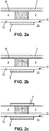
- Figures 2a-2c show two optional improvements of the invention which may be used independently from each other or in combination, in addition to the implementation as illustrated by figures 1a-1c .
- the first improvement consists in using an additional electrolyte portion between the electrolyte portion 1 and one of the electrodes 5 or 6.
- Figure 2a illustrates such additional electrolyte portion as a layer 12 located between the electrode 6 and the electrolyte portion 1.
- Such layer 12 is to be deposited on the surface S of the substrate 10 before the electrolyte portion 1 and the boundary portion 2 are formed.
- another additional electrolyte portion (not represented) may be deposited on the electrolyte portion 1 and the boundary portion 2 after the supply layer 3 has been removed but before the electrode 5 is deposited.
- a possible material for such additional electrolyte portions may be porous aluminium oxide (Al 2 O 3 ) or a chalcogenide material.
- the second improvement consists in using an additional layer 4 which is located between the electrolyte portion 1 and the supply layer 3, as represented in figure 2a .
- additional layer 4 may also extend on the boundary portion 2. Therefore, it is to be deposited on the electrolyte portion 1 and the boundary portion 2 after these latter have been planarized but before the supply layer 3 is deposited.
- the additional layer 4 thus intersects the path of the metal atoms from the supply layer 3 to the electrolyte portion 1.
- the material and thickness of such layer 4, also called liner, are to be selected so that the layer 4 controls the amount of metal atoms that travels from the supply layer 3 to the electrolyte portion 1 during the heating step.
- the layer 4 may be a titanium (Ti) layer, a tantalum (Ta) layer, etc, and its thickness may be 2-3 nm (nanometer).
- An additional function of the optional layer 4 may be forming a stop layer effective during the removal of the supply layer 3 after metal diffusion has been performed.
- the progression of the CMP process which is implemented for removing the supply layer 3 stops when the abrasion surface has reached the layer 4, due to the difference in composition between the layers 3 and 4.
- the layer 4 may be removed after the layer 3 using another etching process suitable for the composition of the layer 4. Appropriate wet etching process may be implemented for example.
- Figure 2b shows the configuration of the circuit being manufactured just after the heating step
- figure 2c corresponds to the configuration of the circuit once the component has been completed.
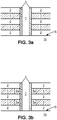
- Figures 3a-3c illustrate another implementation of the invention in which the material portion which has the function of container for the metal atoms is an active electrode for the final component.
- the integrated circuit substrate 10 has a planar upper surface S again. It may have been processed for forming a stack of alternated layers 1 and 2, possibly starting with one layer 2 in particular if the substrate 10 is electrically conducting at its surface S. Then a trench or shaft T is etched through the stack, perpendicular to the surface S and until this latter is reached at the bottom of the trench T. A directional dry etching process may be used for forming the trench T, in a manner which is known in the art.
- the integrated circuit does not contain any amount of the metal to be implemented as migrating and redox species in the final component.
- the supply layer 3 is deposited as a conformal layer in the trench T, for example using an atomic-layer-deposition (ALD) process which is also well-known in the art.
- ALD atomic-layer-deposition
- the material of the supply layer 3 may be again copper, nickel, silver, copper telluride (CuTe), copper-germanium telluride (CuGeTe), an alloy of copper and germanium, etc.
- the layers 1 are intended to host metal atoms for forming active layers. Their constituting material, so-called first material, is thus selected for producing solubility for the metal atoms.
- the layers 2 are intended to act as boundary portions, and thus comprised of a second material which is not permeable to the metal atoms originating from the supply layer 3.
- the first and second materials, of the layers 1 and 2 respectively, may be selected as described above in connection with figure 1a .
- the first material for the layers 1 may be silicon (Si)
- the second material for the layers 2 may be silicon nitride (Si 3 N 4 ).
- the integrated circuit is then heated during a controlled duration and at a controlled temperature, for causing metal atoms to diffuse from the supply layer 3 into the layers 1.
- the diffusion paths are now oriented parallel to the surface S.
- the layers 1 each contain a controlled amount of the metal, whereas the boundary portions 2 do not. These metal amounts are located close to the trench T, in parts of the layers 1 which are denoted 1a in figure 3b . In the parts 1a, the material has been transformed into copper silicide during the heating step.
- the supply layer 3 is then removed, for example using a wet etching process.
- a conformal layer 11 of an electrolyte material is deposited in the trench T in a next step, for example using a suitable ALD deposition process. Then, the electrolyte material may be removed at the bottom of the trench T, for example using a directional dry etching process.
- the material of the electrolyte layer 11 may be an oxide such as porous silica (SiO 2 ) or tungsten oxide (WO), or may be a chalcogenide.
- an electrically conductive material is deposited within the trench T, for at least partially filling it. It forms an inner electrode 5a as shown in figure 3c .
- a CMP process may be implemented thereafter, for removing layer portions of the electrolyte material and of the conductive material which are present on the highest layer 2.
- a top electrode portion 5b is formed above the inner electrode 5a, so as to be in electrical contact with this latter.
- the inner electrode 5a and the top electrode portion 5b form together the inert electrode 5 of the component.
- each layer 1 forms a respective active electrode which pertains to a different component based on metal ion migration and reduction.
- the inert electrode 5 is common to these components.
- copper atoms come out of the layer 1, are oxidized at the interface with the electrolyte layer 11, and then migrate through the electrolyte layer 11 until some of them reach the inner electrode 5a.
- the copper ions are reduced from the interface between the electrolyte layer 11 and the inner electrode 5a, thus forming metal filaments through the electrolyte layer 11.
- the electrical resistance value which exists between the layer 1 of concern and the inert electrode 5 is then low.
- the silicon material of the layers 1 may be replaced with germanium material, or tellurium, or germanium telluride.
- An advantage thereof is an improved soaking of the layers 1 by the metal atoms at the interface with the electrolyte layer 11.
- a liner permeable to the metal atoms may be deposited in a conformal manner in the trench T, before the supply layer 3 is deposited.
- Such liner for example a titanium (Ti) or tantalum (Ta) liner is thus inserted between the layers 1 and the supply layer 3. It allows controlling more accurately the amounts of metal atoms that diffuse into the layers 1 during the heating step.
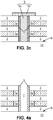
- Figure 4a shows another improvement of the invention implementation of figures 3a-3c .
- the material of the layers 1 may be different in composition in a vicinity of the trench T, as compared to the layers 1 away from the trench T.
- each layer 1 may be comprised of a material optimized for electron transportation and electrical contact away from the trench T, and of another material which is optimized for metal atom insertion and soaking around the trench T. Hence, this another material will have the function of active material during an operation of the final component.
- each layer 1 may be replaced with a chalcogenide-based active material, for example germanium telluride (GeTe), in an area which is centred on the trench T parallel to the surface S, but wider in diameter than the trench T.
- a chalcogenide-based active material for example germanium telluride (GeTe)
- GeTe germanium telluride
- the trench T is etched through the layers 2 and these portions of active material at the levels of the layers 1. Remaining parts of the active material portions surround the trench T parallel to the surface S, and are intended to operate similar to the parts 1a of figures 3b and 3c for hosting the metal atoms.
- the circuit configuration according to this improvement is that shown in figure 4a .
- the circuit manufacturing method can then be continued as described before in connection with the figures 3b (just after the heating step) and 3c (forming of the inert electrode completed).
- component configurations using at least one active electrode can be combined with 2D-configurations.
- component configurations without active electrode, but with reference electrode can be combined with 3D-configurations.
Landscapes
- Chemical & Material Sciences (AREA)
- Engineering & Computer Science (AREA)
- General Chemical & Material Sciences (AREA)
- Chemical Kinetics & Catalysis (AREA)
- Materials Engineering (AREA)
- Mechanical Engineering (AREA)
- Metallurgy (AREA)
- Organic Chemistry (AREA)
- Manufacturing & Machinery (AREA)
- Semiconductor Memories (AREA)
- Internal Circuitry In Semiconductor Integrated Circuit Devices (AREA)
Abstract
Description
- The invention relates to manufacturing of an integrated electronic circuit which includes a component based on metal ion migration and reduction. Such component may be part in particular of a conductive bridging random access memory, denoted CBRAM, a volatile conductive bridge, denoted VCB, or a switch.
- CBRAMs have been identified as a promising technology for the next future, in particular for memory arrays with cross-point design. A bit is stored in such memory element as an electrical conduction state which may be of a low conduction value or a much higher conduction value. Such variation is produced by an electrolyte portion which is in electrical contact with two separate electrodes. Metal ions such as copper or nickel ions are soluble in the electrolyte portion, so that they can migrate therein. Then, when one of the electrodes, called inert electrode, is negatively polarized, the metal ions form continuous tracks which extend between both electrodes, and transform into metal filaments when the tracks reach the inert electrode. The resulting inter-electrode resistance value is very low, and remains such as long as a reversed polarization is not applied. When a suitable reversed polarization is applied, the metal atoms transform back into ions and migrate away from the inert electrode. The inter-electrode resistance value becomes high again.
- Such component based on metal ion migration and reduction may be of two types depending on the source of the metal ions which migrate within the electrolyte portion toward the inert electrode. For the first type, the metal ions originate from the electrode other than the inert electrode, through oxidation at the contact interface between the other electrode and the electrolyte portion. Such other electrode is commonly called active electrode, because material thereof in involved in the oxidation-reduction transformation. Such active electrode is different from the electrolyte portion, and the active electrode and the inert electrode are both in contact with the electrolyte portion, for example on opposed sides thereof. For the second type, both electrodes are inert electrodes arranged apart from each other in contact with the electrolyte portion, and the metal ions are permanently contained within the electrolyte portion, transforming reversibly therein into metal filaments. Switching operation for storing 0- or 1-bit value through resistance value is unchanged.
- At least two issues are to be addressed when manufacturing an integrated electronic circuit which includes such component.
- The first issue is controlling the metal amount for each component, so that operation features are identical between several components designed to be similar within one and same integrated circuit, and also identical between circuit units that are manufactured successively using unchanged manufacture control parameters.
- The second issue is avoiding implementing a dry-etch process for removing a material which contains some of the metal atoms. Indeed, the metal atoms produce unwanted material depositions within the etching tool when being etched, thereby requiring frequent cleaning operations of the inside of the etching tool. The manufacture throughput is reduced for this reason, and the cost price of the integrated circuit is much higher.
- In addition, an object of the present invention may be combining components based on metal ion migration and reduction with a reduction in the substrate area which is occupied by a set of such components.
- For meeting at least one of these objects or others, the present invention proposes a method for manufacturing an integrated electronic circuit which includes at least one component based on metal ion migration and reduction, which method comprises the following steps:
- /1/ selecting a metal and a first material which is different from the metal and capable of containing ions or atoms of the metal, and also selecting at least one second material so that each second material is electrically insulating and has a capacity of containing the metal ions or metal atoms which is less than that of the first material;
- /2/ on a substrate of the integrated circuit, forming at least one portion of the first material, called container, and at least one portion of the at least one second material, called boundary portion, so that the container and the boundary portion are next to each other;
- /3/ depositing a layer on the substrate provided with the container and the boundary portion, said layer containing ions or atoms of the metal and being called supply layer, so that a path from the supply layer to the container is available for some of the ions or atoms of the metal;
- /4/ activating a moving of some of the ions or atoms of the metal that are contained in the supply layer, the moving occurring from the supply layer into at least part of the container selectively with respect to each boundary portion; and
- /5/ removing the supply layer from the integrated circuit, while leaving the ions or atoms of the metal that have moved in step /4/ into the container.
- In various implementations of the invention, the container may be an active electrode, or at least part of an electrolyte portion of the component, or any other part of the component except for the boundary portion.
- According to a first feature of the invention, the method further comprises depositing an electrode portion, called inert electrode, on the integrated circuit being manufactured, so that the component based on metal ion migration and reduction comprises at least the container and the inert electrode. The component based on metal ion migration and reduction is arranged so that metal ions produce metal filaments from the inert electrode within the electrolyte portion when a negative voltage is applied to the inert electrode with respect to the container during an operation of the component, if the container acts as the active electrode capable of transferring electrons outwards in addition to supplying the metal ions or atoms for forming the metal filaments. This corresponds to the first component type described above. Alternatively, for the second component type, the negative voltage is applied to the inert electrode with respect to a reference electrode which is in contact with the electrolyte portion separately from the inert electrode, if the container forms at least part of the electrolyte portion.
- According to a second feature of the invention, the inert electrode when the container acts as an active electrode, or each of the inert electrode and the reference electrode when the container forms at least part of the electrolyte portion, is either not yet formed on the substrate of the integrated circuit before step /5/ has been completed, or isolated from the supply layer by the container or the at least one boundary portion during step /4/.
- In this way, the metal amount within each component is set in step /4/, in a well-defined manner since only the container participates to hosting metal at this time. In particular, the inert electrode and the reference electrode are not polluted with metal atoms during step /4/.
- In addition, step /5/ may be carried out using a removal process other than a dry-etching process. In particular, the supply layer may be removed in step /5/ using a wet etching process or a chemical-mechanical polishing process.
- In various implementations of the invention, the following additional features may be implemented, each separately of in combination of several of them:
- the component based on metal ion migration and reduction may form at least part of a conductive bridging random access memory element, or of a volatile conductive bridge, or of a switch;
- the at least one container may be the only part of the component based on metal ion migration and reduction, which is in contact with the supply layer during step /4/, in addition to the boundary portion(s);
- the moving of some of the ions or atoms of the metal may be activated in step /4/ through heating of the integrated circuit;
- the container may be formed in step /2/ so that it is free of ions and atoms of the metal as resulting directly from this step /2/. In such case, the forming of the container in step /2/ may comprise etching a layer of the first material using a dry-etching process. High integration level is thus possible as the dimensions of the container are defined by lithographic patterning using state-of-the art tools;
- the boundary portion as formed in step /2/ may surround the container, laterally with respect to the path of the metal ions or atoms from the supply layer to the container;
- the invention method may further comprise, between steps /2/ and /3/, depositing an additional layer called liner, of a material which is permeable to the metal ions or atoms during step /4/, for example a liner of tantalum or titanium, so that the liner is intermediate between each container and the supply layer after step /3/. Then, step /5/ further comprises removing the liner after the supply layer. Such liner may help in controlling the metal amount which is inserted into each container, and/or in controlling a process which is implemented for removing the supply layer in step /5/;
- the metal may be copper, nickel or silver, the supply layer possibly being a layer of this metal; and
- the second material may be silicon nitride, aluminum nitride or a mixed nitride of silicon and aluminum.
- The container may act as an active electrode for the first component type, and the first material may be silicon, germanium or tellurium.
- Alternatively, the container may form at least part of the electrolyte portion, corresponding to the second component type recited above. Then, the first material may be an oxide, in particular a tungsten oxide or a silicon oxide, or the first material may be a chalcogenide, in particular germanium telluride or germanium selenide.
- In first possible implementations of the invention, according to so-called 2D-configurations, the container and the boundary portion may be next to each other along at least one direction which is parallel to a surface of the substrate, this surface supporting the component based on metal ion migration and reduction in the integrated circuit. Optionally for such first possible implementations of the invention, the invention method may further comprise forming an electrolyte portion different from the container, so that this electrolyte portion different from the container is between the reference electrode or active electrode and the inert electrode along a direction perpendicular to the substrate surface.
- In second possible implementations of the invention, according to so-called 3D-configurations, step /2/ may comprise forming a stack of several containers and several boundary portions which are alternated along a stacking direction which is perpendicular to a surface of the substrate, this surface supporting the stack. In such case, the method may further comprise, between steps /2/ and /3/, etching a trench or shaft through the containers and boundary portions, parallel to the stacking direction. Then, the supply layer may be deposited in step /3/ as a conformal layer on sidewalls of the trench or shaft, and at least part of the inert electrode is deposited within this trench or shaft so as to fill it at least partially. Such inert electrode is thus common to several components each based on migration and reduction of the metal ions but each corresponding to a respective one of the containers. Optionally for such second possible implementations of the invention, the method may further comprise, after step /5/ but before the inert electrode is deposited, depositing an electrolyte portion different from the containers as another conformal layer on the sidewalls of the trench or shaft, so that this electrolyte portion different from the container is in contact with the containers through the sidewalls of the trench or shaft, and also in contact with the inert electrode in the trench or shaft. Such electrolyte portion different from the containers is then also common to the components each based on migration and reduction of the metal ions but each corresponding to a respective one of the containers.
- These and other features of the invention will be now described with reference to the appended figures, which relate to preferred but not-limiting implementations of the invention.
-
-
Figures 1a-1c are cross-sectional views of an integrated circuit being manufactured according to a first 2D-implementation of the invention. -
Figures 2a-2c correspond tofigures 1a-1c , respectively, for a second 2D-implementation of the invention. -
Figures 3a-3c are cross-sectional views of another integrated circuit being manufactured, but according to a first 3D-implementation of the invention. -
Figure 4a corresponds tofigure 3a for a second 3D-implementation of the invention. - For clarity sake, element sizes which appear in these figures do not correspond to actual dimensions or dimension ratios. Also, same reference numbers which are indicated in different ones of these figures denote identical elements of elements with identical function.
- According to
figure 1a , anintegrated circuit substrate 10 has a planar upper surface S. Thesubstrate 10 may have been processed beforehand so that it is electrically insulating at its surface S outside of anelectrode 6. Theelectrode 6 is flush with the substrate surface S. For example, theelectrode 6 is copper-based or comprised of titanium nitride (TiN), and is surrounded with silica (SiO2) material within thesubstrate 10. Then a pattern of at least oneportion 1 of a first material is formed on the surface S, on theelectrode 6, and surrounded by a layer portion of asecond material 2. Thefirst material portion 1 may be intended to form the electrolyte portion in the final component, and be the container in the implementation described now, and the secondmaterial layer portion 2 may be intended to form a boundary portion such that metal atoms cannot travel out of theportion 1 parallel to the surface S. Thus, atoms or ions of the metal exhibit solubility and mobility in the first material, whereas they can almost not be incorporated into the second material. In a known manner, for example fromEP 3 029 683electrolyte portion 1, when compared to the same metal but in the second material used for theboundary portion 2. - Suitable metals are copper (Cu), nickel (Ni), silver (Ag), etc.
- The first material for the
electrolyte portion 1 may be porous silicon oxide (SiOx) or tungsten oxide (WOx), or another oxide, or may be a chalcogenide material such as germanium telluride (GeTe), germanium selenide (GeSe), germanium sulfide (GeS), silicon telluride (SiTe), etc. Metal ions or atoms are mobile within such first material, for example when submitted to an electrical field, and can transform reversibly from ions to atoms. - The second material for the
boundary portion 2 may be silicon nitride (Si3N4), aluminium nitride (AlN), mixed silicon and aluminium nitride, dense silica such as thermal silica, etc. - The
electrolyte portion 1 may be formed at first on the surface S, for example through material layer deposition and selective dry-etching using a mask, and then embedded within a layer of the second material. The first material, i.e. the electrolyte material, and the second material are thus deposited free of metal content. Then, the upper surface of the layer of the second material can be planarized, for example using a chemical-mechanical polishing process (CMP), until theelectrolyte portion 1 becomes exposed. Preferably, theboundary portion 2 surrounds theelectrolyte portion 1 in projection onto the surface S. - A
layer 3 of a metal-containing material is then deposited on theelectrolyte portion 1 and theboundary portion 2, opposite thesubstrate 10. For example, if the metal is copper, thelayer 3 may be a copper layer, or a layer of copper telluride (CuTe), copper-germanium telluride (CuGeTe), an alloy of copper and germanium, etc. Circuit configuration shown infigure 1a is thus obtained. - The integrated circuit is heated during controlled duration and at controlled temperature, so that an amount of metal diffuses from the
layer 3 into theelectrolyte portion 1, selectively with respect to theboundary portion 2. The diffusion path is mainly oriented perpendicular to the surface S. At the end of the heating step, theelectrolyte portion 1 contains a controlled amount of the metal, whereas theboundary portion 2 does not. The heating duration may also be controlled so that metal atoms originating from thelayer 3 do not reach theelectrode 6. Circuit configuration as shown infigure 1b is obtained, wherereference sign 1a denotes a part of theelectrolyte portion 1 which has been penetrated by metal atoms during the heating step. Thelayer 3 has the function of a supply layer for the metal atoms penetrated into theelectrolyte portion 1, and this latter has a function of a container for the metal atoms to remain in the final circuit. - Also the material of the
electrode 6 may have been selected so that metal atoms which would thermally diffuse through thewhole electrolyte portion 1 and reach theelectrode 6 do not penetrate this latter. Thus the metal amount which is absorbed into the existing part of the circuit is even more controlled. - Then the
layer 3 as existing after the heating step is removed from the circuit, for example using a suitable chemical-mechanical polishing process (CMP). The removal process is continued until theelectrolyte portion 1 and theboundary portion 2 are exposed. The component is completed in a next step by forming anotherelectrode 5 above theelectrolyte portion 1, and in contact with it. For such structure of the component based on migration and reduction of the metal ions, bothelectrodes electrodes electrolyte portion 1, and thus producing the low electrical resistance value between bothelectrodes electrode 5 corresponds to the inert electrode as mentioned in the general part of this description, and theelectrode 6 is reference electrode. - For example, a component based on metal ion migration and reduction as described with reference to
figures 1a-1c may be a conductive bridging RAM. Then, theelectrode 5 may be part of a word line, and theelectrode 6 may be part of a bit line. - The component may also be a volatile conductive bridge, which can be used as a selector device in a memory point array.
- Possibly, a first component forming a conductive bridging RAM may be combined in series with a second component forming a volatile conductive bridge, thereby forming a serial selector in a memory cell, according to a 1-selector 1-resistor configuration. Both first and second components may have been each obtained according to the present invention.
-
Figures 2a-2c show two optional improvements of the invention which may be used independently from each other or in combination, in addition to the implementation as illustrated byfigures 1a-1c . - The first improvement consists in using an additional electrolyte portion between the
electrolyte portion 1 and one of theelectrodes Figure 2a illustrates such additional electrolyte portion as alayer 12 located between theelectrode 6 and theelectrolyte portion 1.Such layer 12 is to be deposited on the surface S of thesubstrate 10 before theelectrolyte portion 1 and theboundary portion 2 are formed. Alternatively or in combination, another additional electrolyte portion (not represented) may be deposited on theelectrolyte portion 1 and theboundary portion 2 after thesupply layer 3 has been removed but before theelectrode 5 is deposited. A possible material for such additional electrolyte portions may be porous aluminium oxide (Al2O3) or a chalcogenide material. - The second improvement consists in using an
additional layer 4 which is located between theelectrolyte portion 1 and thesupply layer 3, as represented infigure 2a . Suchadditional layer 4 may also extend on theboundary portion 2. Therefore, it is to be deposited on theelectrolyte portion 1 and theboundary portion 2 after these latter have been planarized but before thesupply layer 3 is deposited. Theadditional layer 4 thus intersects the path of the metal atoms from thesupply layer 3 to theelectrolyte portion 1. The material and thickness ofsuch layer 4, also called liner, are to be selected so that thelayer 4 controls the amount of metal atoms that travels from thesupply layer 3 to theelectrolyte portion 1 during the heating step. Improved control of this metal amount is provided by implementing thelayer 4, thanks to the permeability of thelayer 4 to the metal atoms. For example, thelayer 4 may be a titanium (Ti) layer, a tantalum (Ta) layer, etc, and its thickness may be 2-3 nm (nanometer). - An additional function of the
optional layer 4 may be forming a stop layer effective during the removal of thesupply layer 3 after metal diffusion has been performed. The progression of the CMP process which is implemented for removing thesupply layer 3 stops when the abrasion surface has reached thelayer 4, due to the difference in composition between thelayers layer 4 may be removed after thelayer 3 using another etching process suitable for the composition of thelayer 4. Appropriate wet etching process may be implemented for example. -
Figure 2b shows the configuration of the circuit being manufactured just after the heating step, andfigure 2c corresponds to the configuration of the circuit once the component has been completed. -
Figures 3a-3c illustrate another implementation of the invention in which the material portion which has the function of container for the metal atoms is an active electrode for the final component. Theintegrated circuit substrate 10 has a planar upper surface S again. It may have been processed for forming a stack of alternatedlayers layer 2 in particular if thesubstrate 10 is electrically conducting at its surface S. Then a trench or shaft T is etched through the stack, perpendicular to the surface S and until this latter is reached at the bottom of the trench T. A directional dry etching process may be used for forming the trench T, in a manner which is known in the art. Until this stage of the manufacturing method, the integrated circuit does not contain any amount of the metal to be implemented as migrating and redox species in the final component. Then thesupply layer 3 is deposited as a conformal layer in the trench T, for example using an atomic-layer-deposition (ALD) process which is also well-known in the art. The circuit configuration shown infigure 3a is obtained. - The material of the
supply layer 3 may be again copper, nickel, silver, copper telluride (CuTe), copper-germanium telluride (CuGeTe), an alloy of copper and germanium, etc. Thelayers 1 are intended to host metal atoms for forming active layers. Their constituting material, so-called first material, is thus selected for producing solubility for the metal atoms. Thelayers 2 are intended to act as boundary portions, and thus comprised of a second material which is not permeable to the metal atoms originating from thesupply layer 3. The first and second materials, of thelayers figure 1a . For example, the first material for thelayers 1 may be silicon (Si), and the second material for thelayers 2 may be silicon nitride (Si3N4). - The integrated circuit is then heated during a controlled duration and at a controlled temperature, for causing metal atoms to diffuse from the
supply layer 3 into thelayers 1. The diffusion paths are now oriented parallel to the surface S. At the end of the heating step, thelayers 1 each contain a controlled amount of the metal, whereas theboundary portions 2 do not. These metal amounts are located close to the trench T, in parts of thelayers 1 which are denoted 1a infigure 3b . In theparts 1a, the material has been transformed into copper silicide during the heating step. - The
supply layer 3 is then removed, for example using a wet etching process. Aconformal layer 11 of an electrolyte material is deposited in the trench T in a next step, for example using a suitable ALD deposition process. Then, the electrolyte material may be removed at the bottom of the trench T, for example using a directional dry etching process. The material of theelectrolyte layer 11 may be an oxide such as porous silica (SiO2) or tungsten oxide (WO), or may be a chalcogenide. Then an electrically conductive material is deposited within the trench T, for at least partially filling it. It forms aninner electrode 5a as shown infigure 3c . A CMP process may be implemented thereafter, for removing layer portions of the electrolyte material and of the conductive material which are present on thehighest layer 2. Finally, atop electrode portion 5b is formed above theinner electrode 5a, so as to be in electrical contact with this latter. Theinner electrode 5a and thetop electrode portion 5b form together theinert electrode 5 of the component. - During an operation of such circuit, each
layer 1 forms a respective active electrode which pertains to a different component based on metal ion migration and reduction. Theinert electrode 5 is common to these components. When a positive voltage is applied to one of thelayers 1 with respect to theinert electrode 5, so that this latter appears to be polarized negatively, copper atoms come out of thelayer 1, are oxidized at the interface with theelectrolyte layer 11, and then migrate through theelectrolyte layer 11 until some of them reach theinner electrode 5a. The copper ions are reduced from the interface between theelectrolyte layer 11 and theinner electrode 5a, thus forming metal filaments through theelectrolyte layer 11. The electrical resistance value which exists between thelayer 1 of concern and theinert electrode 5 is then low. Inverting the electrical polarization between thelayer 1 and theinert electrode 5, so that this latter is now positively biased, produces oxidation of the copper atoms which are inside theelectrolyte layer 11 or at the interface thereof with theinner electrode 5a. The metal ions then migrate back to thelayer 1, and penetrate into thepart 1a of this latter to form recovered copper silicide. In this way, theparts 1a of thelayers 1 which have the function of containers for the metal atoms in the manufacturing method of the invention have the function of active electrodes during operations of the final component. - In alternative implementations of the invention, the silicon material of the
layers 1 may be replaced with germanium material, or tellurium, or germanium telluride. An advantage thereof is an improved soaking of thelayers 1 by the metal atoms at the interface with theelectrolyte layer 11. - In a manner similar to that illustrated by
figure 2a and 2b , a liner permeable to the metal atoms may be deposited in a conformal manner in the trench T, before thesupply layer 3 is deposited. Such liner, for example a titanium (Ti) or tantalum (Ta) liner is thus inserted between thelayers 1 and thesupply layer 3. It allows controlling more accurately the amounts of metal atoms that diffuse into thelayers 1 during the heating step. -
Figure 4a shows another improvement of the invention implementation offigures 3a-3c . When forming initially the stack of thelayers substrate 10, the material of thelayers 1 may be different in composition in a vicinity of the trench T, as compared to thelayers 1 away from the trench T. For example, eachlayer 1 may be comprised of a material optimized for electron transportation and electrical contact away from the trench T, and of another material which is optimized for metal atom insertion and soaking around the trench T. Hence, this another material will have the function of active material during an operation of the final component. For example, the silicon material of eachlayer 1 may be replaced with a chalcogenide-based active material, for example germanium telluride (GeTe), in an area which is centred on the trench T parallel to the surface S, but wider in diameter than the trench T. Then, the trench T is etched through thelayers 2 and these portions of active material at the levels of thelayers 1. Remaining parts of the active material portions surround the trench T parallel to the surface S, and are intended to operate similar to theparts 1a offigures 3b and3c for hosting the metal atoms. After thesupply layer 3 has been deposited in a conformal manner within the trench T, the circuit configuration according to this improvement is that shown infigure 4a . The circuit manufacturing method can then be continued as described before in connection with thefigures 3b (just after the heating step) and 3c (forming of the inert electrode completed). - The Man skilled in the art will understand than the implementations of the invention described above can be varied for secondary aspects thereof, while maintaining the advantages which have been cited. In particular, component configurations using at least one active electrode can be combined with 2D-configurations. Also, component configurations without active electrode, but with reference electrode, can be combined with 3D-configurations.
- Finally, it is reminded that all materials have been mentioned for illustrative purpose only, and that the optional improvements of the invention which have been described can be combined with one another in an obvious manner.
Claims (17)
- A method for manufacturing an integrated electronic circuit which includes at least one component based on metal ion migration and reduction, which method comprises the following steps:/1/ selecting a metal and a first material which is different from the metal and capable of containing ions or atoms of the metal, and also selecting at least one second material so that each second material is electrically insulating and has a capacity of containing the metal ions or metal atoms which is less than that of the first material;/2/on a substrate (10) of the integrated circuit, forming at least one portion of the first material, called container (1), and at least one portion of the at least one second material, called boundary portion (2), so that the container and the boundary portion are next to each other;/3/ depositing a layer on the substrate provided with the container and the boundary portion, said layer containing ions or atoms of the metal and being called supply layer (3), so that a path from the supply layer to the container (1) is available for some of said ions or atoms of the metal;/4/ activating a moving of some of the ions or atoms of the metal that are contained in the supply layer (3), said moving occurring from said supply layer into at least part of the container (1) selectively with respect to each boundary portion (2); and/5/ removing the supply layer (3) from the integrated circuit, while leaving the ions or atoms of the metal that have moved in step /4/ into the container (1),wherein the method further comprises depositing an electrode portion, called inert electrode (5), on the integrated circuit, so that the component based on metal ion migration and reduction comprises at least the container (1) and the inert electrode,
the component based on metal ion migration and reduction being arranged so that metal ions produce metal filaments from the inert electrode (5) within an electrolyte portion (11; 12) when a negative voltage is applied to said inert electrode with respect to the container (1) if said container acts as an active electrode capable of transferring electrons outwards in addition to supplying the metal ions or atoms for forming the metal filaments, or with respect to a reference electrode (6) which is in contact with the electrolyte portion separately from the inert electrode if said container forms at least part of the electrolyte portion, during an operation of the component,
and wherein the inert electrode (5) when the container (1) acts as an active electrode, or each of the inert electrode (5) and the reference electrode (6) when the container forms at least part of the electrolyte portion, is either not yet formed on the substrate (10) of the integrated circuit before /5/ has been completed, or isolated from the supply layer (3) by the container (1) or the at least one boundary portion during step /4/. - The method of claim 1, wherein the component based on metal ion migration and reduction forms at least part of a conductive bridging random access memory element, or of a volatile conductive bridge, or of a switch.
- The method of claim 1 or 2, wherein the at least one container (1) is the only part of the component based on metal ion migration and reduction, which is in contact with the supply layer (3) during step /4/, in addition to the boundary portion (2).
- The method of any one of the preceding claims, wherein the moving of some of the ions or atoms of the metal is activated in step /4/ through heating of the integrated circuit.
- The method of any one of claims 1 to 4, wherein the container (1) is formed in step /2/ so that said container is free of ions and atoms of the metal as resulting directly from said step /2/.
- The method of claim 5, wherein the forming of the container (1) in step /2/ comprises etching a layer of the first material using a dry-etching process.
- The method of any one of the preceding claims, wherein the boundary portion (2) as formed in step /2/ surrounds the container (1), laterally with respect to the path of the metal ions or atoms from the supply layer (3) to the container.
- The method of any one of claims 1 to 7, wherein the container (1) and the boundary portion (2) are next to each other along at least one direction parallel to a surface (S) of the substrate (10), said surface supporting the component based on metal ion migration and reduction in the integrated circuit.
- The method of claim 8, further comprising forming an electrolyte portion (12) different from the container (1), so that said electrolyte portion different from the container is between the reference electrode (6) or active electrode and the inert electrode (5) along a direction perpendicular to the substrate surface (S).
- The method of any one of claims 1 to 7, wherein step /2/ comprises forming a stack of several containers (1) and several boundary portions (2) which are alternated along a stacking direction which is perpendicular to a surface (S) of the substrate (10), said surface supporting the stack,
the method further comprising, between steps /2/ and /3/, etching a trench (T) or shaft through the containers (1) and boundary portions (2), parallel to the stacking direction,
then the supply layer (3) is deposited in step /3/ as a conformal layer on sidewalls of the trench (T) or shaft, and
the method further comprises depositing at least part of the inert electrode (5) within said trench (T) or shaft so as to fill at least partially said trench or shaft, said inert electrode being common to several components each based on migration and reduction of the metal ions but each corresponding to a respective one of the containers (1). - The method of claim 10, further comprising, after step /5/ but before the inert electrode (5) is deposited, depositing an electrolyte portion (11) different from the containers (1) as another conformal layer on the sidewalls of the trench (T) or shaft, so that said electrolyte portion different from the container is in contact with the containers through the sidewalls of the trench or shaft and in contact with the inert electrode in the trench or shaft,
said electrolyte portion (11) different from the containers (1) being common to the components each based on migration and reduction of the metal ions but each corresponding to a respective one of the containers. - The method of any one of the preceding claims, wherein the supply layer (3) is removed in step /5/ using a wet etching process or a chemical-mechanical polishing process.
- The method of any one of the preceding claims, further comprising, between steps /2/ and /3/, depositing an additional layer called liner (4), of a material which is permeable to the metal ions or atoms during step /4/, for example a liner of tantalum or titanium, so that the liner is intermediate between each container (1) and the supply layer (3) after step /3/,
and wherein step /5/ further comprises removing the liner (4) after the supply layer (3). - The method of any one of the preceding claims, wherein the metal is copper, nickel or silver, the supply layer (3) possibly being a layer of said metal.
- The method of any one of the preceding claims, wherein the second material is silicon nitride, aluminum nitride or a mixed nitride of silicon and aluminum.
- The method of any one of claims 1 to 15, wherein the container (1) acts as an active electrode, and the first material is silicon, germanium, or tellurium.
- The method of any one of claims 1 to 15, wherein the container (1) forms at least part of the electrolyte portion, and the first material is an oxide, in particular a tungsten oxide or a silicon oxide, or the first material is a chalcogenide, in particular germanium telluride or germanium selenide.
Priority Applications (2)
| Application Number | Priority Date | Filing Date | Title |
|---|---|---|---|
| EP18306168.8A EP3621126B1 (en) | 2018-09-05 | 2018-09-05 | Manufacturing of an integrated electronic circuit which includes a component based on metal ion migration and reduction |
| US16/560,777 US11075337B2 (en) | 2018-09-05 | 2019-09-04 | Integrated circuit devices based on metal ion migration and methods of fabricating same |
Applications Claiming Priority (1)
| Application Number | Priority Date | Filing Date | Title |
|---|---|---|---|
| EP18306168.8A EP3621126B1 (en) | 2018-09-05 | 2018-09-05 | Manufacturing of an integrated electronic circuit which includes a component based on metal ion migration and reduction |
Publications (2)
| Publication Number | Publication Date |
|---|---|
| EP3621126A1 true EP3621126A1 (en) | 2020-03-11 |
| EP3621126B1 EP3621126B1 (en) | 2021-06-16 |
Family
ID=63683124
Family Applications (1)
| Application Number | Title | Priority Date | Filing Date |
|---|---|---|---|
| EP18306168.8A Active EP3621126B1 (en) | 2018-09-05 | 2018-09-05 | Manufacturing of an integrated electronic circuit which includes a component based on metal ion migration and reduction |
Country Status (2)
| Country | Link |
|---|---|
| US (1) | US11075337B2 (en) |
| EP (1) | EP3621126B1 (en) |
Families Citing this family (2)
| Publication number | Priority date | Publication date | Assignee | Title |
|---|---|---|---|---|
| JPWO2021039988A1 (en) * | 2019-08-30 | 2021-03-04 | ||
| JP2024019960A (en) * | 2022-08-01 | 2024-02-14 | キヤノン株式会社 | Photoelectric conversion devices and equipment |
Citations (5)
| Publication number | Priority date | Publication date | Assignee | Title |
|---|---|---|---|---|
| US20120133026A1 (en) * | 2008-10-29 | 2012-05-31 | Jianhua Yang | Electrically Actuated Device And Method Of Controlling The Formation Of Dopants Therein |
| US9076723B1 (en) * | 2014-03-10 | 2015-07-07 | Kabushiki Kaisha Toshiba | Non-volatile memory device and method for manufacturing same |
| US20150213887A1 (en) * | 2014-01-28 | 2015-07-30 | Kabushiki Kaisha Toshiba | Semiconductor memory device |
| EP3029683A1 (en) | 2014-12-02 | 2016-06-08 | IMEC vzw | Conductive bridging memory device |
| US20170077100A1 (en) * | 2015-09-11 | 2017-03-16 | Kabushiki Kaisha Toshiba | Nonvolatile memory device manufacturing method |
Family Cites Families (10)
| Publication number | Priority date | Publication date | Assignee | Title |
|---|---|---|---|---|
| DE102004061548A1 (en) | 2004-12-21 | 2006-06-29 | Infineon Technologies Ag | Memory cell matrix for integration of solid electrolyte memory cells has word line and plate line that are controlled by means of selection transistor and exhibits common plate electrode which is connected to common plate circuit |
| US20090213643A1 (en) * | 2008-02-26 | 2009-08-27 | Michael Angerbauer | Integrated Circuit and Method of Improved Determining a Memory State of a Memory Cell |
| US8168468B2 (en) | 2008-02-29 | 2012-05-01 | Freescale Semiconductor, Inc. | Method of making a semiconductor device including a bridgeable material |
| FR2934711B1 (en) * | 2008-07-29 | 2011-03-11 | Commissariat Energie Atomique | MEMORY DEVICE AND CBRAM MEMORY WITH IMPROVED RELIABILITY. |
| US8426839B1 (en) * | 2009-04-24 | 2013-04-23 | Adesto Technologies Corporation | Conducting bridge random access memory (CBRAM) device structures |
| US8198124B2 (en) * | 2010-01-05 | 2012-06-12 | Micron Technology, Inc. | Methods of self-aligned growth of chalcogenide memory access device |
| US8962460B2 (en) | 2011-04-26 | 2015-02-24 | Micron Technology, Inc. | Methods of selectively forming metal-doped chalcogenide materials, methods of selectively doping chalcogenide materials, and methods of forming semiconductor device structures including same |
| JP2013175524A (en) | 2012-02-23 | 2013-09-05 | Toshiba Corp | Semiconductor device and method of manufacturing the same |
| FR3003401B1 (en) | 2013-03-15 | 2016-12-09 | Altis Semiconductor Snc | MICROELECTRONIC DEVICE WITH PROGRAMMABLE MEMORY |
| US10312288B2 (en) | 2015-04-06 | 2019-06-04 | Nec Corporation | Switching element, semiconductor device, and semiconductor device manufacturing method |
-
2018
- 2018-09-05 EP EP18306168.8A patent/EP3621126B1/en active Active
-
2019
- 2019-09-04 US US16/560,777 patent/US11075337B2/en active Active
Patent Citations (5)
| Publication number | Priority date | Publication date | Assignee | Title |
|---|---|---|---|---|
| US20120133026A1 (en) * | 2008-10-29 | 2012-05-31 | Jianhua Yang | Electrically Actuated Device And Method Of Controlling The Formation Of Dopants Therein |
| US20150213887A1 (en) * | 2014-01-28 | 2015-07-30 | Kabushiki Kaisha Toshiba | Semiconductor memory device |
| US9076723B1 (en) * | 2014-03-10 | 2015-07-07 | Kabushiki Kaisha Toshiba | Non-volatile memory device and method for manufacturing same |
| EP3029683A1 (en) | 2014-12-02 | 2016-06-08 | IMEC vzw | Conductive bridging memory device |
| US20170077100A1 (en) * | 2015-09-11 | 2017-03-16 | Kabushiki Kaisha Toshiba | Nonvolatile memory device manufacturing method |
Also Published As
| Publication number | Publication date |
|---|---|
| US11075337B2 (en) | 2021-07-27 |
| EP3621126B1 (en) | 2021-06-16 |
| US20200075849A1 (en) | 2020-03-05 |
Similar Documents
| Publication | Publication Date | Title |
|---|---|---|
| KR102568279B1 (en) | Via Formation for Memory Devices | |
| US9000408B2 (en) | Memory device with low reset current | |
| KR101620396B1 (en) | Methods for forming electrodes in phase change memory devices | |
| CN101197423B (en) | Method of manufacturing self-converging memory material elements in memory cells | |
| TWI515836B (en) | Method for forming a memory cell using a gas cluster ion beam | |
| US20090242865A1 (en) | Memory array with diode driver and method for fabricating the same | |
| US20110147695A1 (en) | Fabricating current-confining structures in phase change memory switch cells | |
| CN110875429A (en) | Switching element, variable resistance memory device, and method of manufacturing switching element | |
| US20120267601A1 (en) | Phase change memory cells with surfactant layers | |
| US10833267B2 (en) | Structure and method to form phase change memory cell with self- align top electrode contact | |
| KR102323249B1 (en) | Semiconductor including data storage pattern | |
| TW201143083A (en) | Methods of self-aligned growth of chalcogenide memory access device | |
| CN111146340A (en) | A phase change memory cell and method of making the same | |
| US20180331284A1 (en) | Threshold voltage control of memory cell selector for phase change and resistive random access memory arrays | |
| JP2023552038A (en) | Phase change memory cell with projection liner | |
| KR100713936B1 (en) | Phase change memory device and manufacturing method thereof | |
| US7329561B2 (en) | Fabricating memory components (PCRAMS) including memory cells based on a layer that changes phase state | |
| US11075337B2 (en) | Integrated circuit devices based on metal ion migration and methods of fabricating same | |
| US11672130B2 (en) | Semiconductor device and method of forming the same | |
| KR101026603B1 (en) | Manufacturing method of phase change memory device | |
| US11380842B2 (en) | Phase change memory cell with second conductive layer | |
| KR20110076764A (en) | Phase change structure, formation method of phase change material layer, phase change memory device and manufacturing method of phase change memory device | |
| JP2006344948A (en) | Phase transformation memory element and its manufacturing method | |
| KR20210000730A (en) | Fabrication of electrodes for memory cells | |
| US12256653B2 (en) | PCM cell with nanoheater surrounded with airgaps |
Legal Events
| Date | Code | Title | Description |
|---|---|---|---|
| PUAI | Public reference made under article 153(3) epc to a published international application that has entered the european phase |
Free format text: ORIGINAL CODE: 0009012 |
|
| STAA | Information on the status of an ep patent application or granted ep patent |
Free format text: STATUS: THE APPLICATION HAS BEEN PUBLISHED |
|
| AK | Designated contracting states |
Kind code of ref document: A1 Designated state(s): AL AT BE BG CH CY CZ DE DK EE ES FI FR GB GR HR HU IE IS IT LI LT LU LV MC MK MT NL NO PL PT RO RS SE SI SK SM TR |
|
| AX | Request for extension of the european patent |
Extension state: BA ME |
|
| STAA | Information on the status of an ep patent application or granted ep patent |
Free format text: STATUS: REQUEST FOR EXAMINATION WAS MADE |
|
| 17P | Request for examination filed |
Effective date: 20200902 |
|
| RBV | Designated contracting states (corrected) |
Designated state(s): AL AT BE BG CH CY CZ DE DK EE ES FI FR GB GR HR HU IE IS IT LI LT LU LV MC MK MT NL NO PL PT RO RS SE SI SK SM TR |
|
| GRAP | Despatch of communication of intention to grant a patent |
Free format text: ORIGINAL CODE: EPIDOSNIGR1 |
|
| STAA | Information on the status of an ep patent application or granted ep patent |
Free format text: STATUS: GRANT OF PATENT IS INTENDED |
|
| INTG | Intention to grant announced |
Effective date: 20210209 |
|
| GRAS | Grant fee paid |
Free format text: ORIGINAL CODE: EPIDOSNIGR3 |
|
| GRAA | (expected) grant |
Free format text: ORIGINAL CODE: 0009210 |
|
| STAA | Information on the status of an ep patent application or granted ep patent |
Free format text: STATUS: THE PATENT HAS BEEN GRANTED |
|
| AK | Designated contracting states |
Kind code of ref document: B1 Designated state(s): AL AT BE BG CH CY CZ DE DK EE ES FI FR GB GR HR HU IE IS IT LI LT LU LV MC MK MT NL NO PL PT RO RS SE SI SK SM TR |
|
| REG | Reference to a national code |
Ref country code: GB Ref legal event code: FG4D |
|
| REG | Reference to a national code |
Ref country code: CH Ref legal event code: EP |
|
| REG | Reference to a national code |
Ref country code: DE Ref legal event code: R096 Ref document number: 602018018636 Country of ref document: DE |
|
| REG | Reference to a national code |
Ref country code: AT Ref legal event code: REF Ref document number: 1403074 Country of ref document: AT Kind code of ref document: T Effective date: 20210715 |
|
| REG | Reference to a national code |
Ref country code: IE Ref legal event code: FG4D |
|
| REG | Reference to a national code |
Ref country code: LT Ref legal event code: MG9D |
|
| PG25 | Lapsed in a contracting state [announced via postgrant information from national office to epo] |
Ref country code: LT Free format text: LAPSE BECAUSE OF FAILURE TO SUBMIT A TRANSLATION OF THE DESCRIPTION OR TO PAY THE FEE WITHIN THE PRESCRIBED TIME-LIMIT Effective date: 20210616 Ref country code: HR Free format text: LAPSE BECAUSE OF FAILURE TO SUBMIT A TRANSLATION OF THE DESCRIPTION OR TO PAY THE FEE WITHIN THE PRESCRIBED TIME-LIMIT Effective date: 20210616 Ref country code: FI Free format text: LAPSE BECAUSE OF FAILURE TO SUBMIT A TRANSLATION OF THE DESCRIPTION OR TO PAY THE FEE WITHIN THE PRESCRIBED TIME-LIMIT Effective date: 20210616 Ref country code: BG Free format text: LAPSE BECAUSE OF FAILURE TO SUBMIT A TRANSLATION OF THE DESCRIPTION OR TO PAY THE FEE WITHIN THE PRESCRIBED TIME-LIMIT Effective date: 20210916 |
|
| REG | Reference to a national code |
Ref country code: AT Ref legal event code: MK05 Ref document number: 1403074 Country of ref document: AT Kind code of ref document: T Effective date: 20210616 |
|
| REG | Reference to a national code |
Ref country code: NL Ref legal event code: MP Effective date: 20210616 |
|
| PG25 | Lapsed in a contracting state [announced via postgrant information from national office to epo] |
Ref country code: LV Free format text: LAPSE BECAUSE OF FAILURE TO SUBMIT A TRANSLATION OF THE DESCRIPTION OR TO PAY THE FEE WITHIN THE PRESCRIBED TIME-LIMIT Effective date: 20210616 Ref country code: NO Free format text: LAPSE BECAUSE OF FAILURE TO SUBMIT A TRANSLATION OF THE DESCRIPTION OR TO PAY THE FEE WITHIN THE PRESCRIBED TIME-LIMIT Effective date: 20210916 Ref country code: SE Free format text: LAPSE BECAUSE OF FAILURE TO SUBMIT A TRANSLATION OF THE DESCRIPTION OR TO PAY THE FEE WITHIN THE PRESCRIBED TIME-LIMIT Effective date: 20210616 Ref country code: RS Free format text: LAPSE BECAUSE OF FAILURE TO SUBMIT A TRANSLATION OF THE DESCRIPTION OR TO PAY THE FEE WITHIN THE PRESCRIBED TIME-LIMIT Effective date: 20210616 Ref country code: GR Free format text: LAPSE BECAUSE OF FAILURE TO SUBMIT A TRANSLATION OF THE DESCRIPTION OR TO PAY THE FEE WITHIN THE PRESCRIBED TIME-LIMIT Effective date: 20210917 |
|
| PG25 | Lapsed in a contracting state [announced via postgrant information from national office to epo] |
Ref country code: EE Free format text: LAPSE BECAUSE OF FAILURE TO SUBMIT A TRANSLATION OF THE DESCRIPTION OR TO PAY THE FEE WITHIN THE PRESCRIBED TIME-LIMIT Effective date: 20210616 Ref country code: ES Free format text: LAPSE BECAUSE OF FAILURE TO SUBMIT A TRANSLATION OF THE DESCRIPTION OR TO PAY THE FEE WITHIN THE PRESCRIBED TIME-LIMIT Effective date: 20210616 Ref country code: SM Free format text: LAPSE BECAUSE OF FAILURE TO SUBMIT A TRANSLATION OF THE DESCRIPTION OR TO PAY THE FEE WITHIN THE PRESCRIBED TIME-LIMIT Effective date: 20210616 Ref country code: SK Free format text: LAPSE BECAUSE OF FAILURE TO SUBMIT A TRANSLATION OF THE DESCRIPTION OR TO PAY THE FEE WITHIN THE PRESCRIBED TIME-LIMIT Effective date: 20210616 Ref country code: CZ Free format text: LAPSE BECAUSE OF FAILURE TO SUBMIT A TRANSLATION OF THE DESCRIPTION OR TO PAY THE FEE WITHIN THE PRESCRIBED TIME-LIMIT Effective date: 20210616 Ref country code: AT Free format text: LAPSE BECAUSE OF FAILURE TO SUBMIT A TRANSLATION OF THE DESCRIPTION OR TO PAY THE FEE WITHIN THE PRESCRIBED TIME-LIMIT Effective date: 20210616 Ref country code: NL Free format text: LAPSE BECAUSE OF FAILURE TO SUBMIT A TRANSLATION OF THE DESCRIPTION OR TO PAY THE FEE WITHIN THE PRESCRIBED TIME-LIMIT Effective date: 20210616 Ref country code: RO Free format text: LAPSE BECAUSE OF FAILURE TO SUBMIT A TRANSLATION OF THE DESCRIPTION OR TO PAY THE FEE WITHIN THE PRESCRIBED TIME-LIMIT Effective date: 20210616 Ref country code: PT Free format text: LAPSE BECAUSE OF FAILURE TO SUBMIT A TRANSLATION OF THE DESCRIPTION OR TO PAY THE FEE WITHIN THE PRESCRIBED TIME-LIMIT Effective date: 20211018 |
|
| PG25 | Lapsed in a contracting state [announced via postgrant information from national office to epo] |
Ref country code: PL Free format text: LAPSE BECAUSE OF FAILURE TO SUBMIT A TRANSLATION OF THE DESCRIPTION OR TO PAY THE FEE WITHIN THE PRESCRIBED TIME-LIMIT Effective date: 20210616 |
|
| REG | Reference to a national code |
Ref country code: DE Ref legal event code: R097 Ref document number: 602018018636 Country of ref document: DE |
|
| PLBE | No opposition filed within time limit |
Free format text: ORIGINAL CODE: 0009261 |
|
| STAA | Information on the status of an ep patent application or granted ep patent |
Free format text: STATUS: NO OPPOSITION FILED WITHIN TIME LIMIT |
|
| PG25 | Lapsed in a contracting state [announced via postgrant information from national office to epo] |
Ref country code: DK Free format text: LAPSE BECAUSE OF FAILURE TO SUBMIT A TRANSLATION OF THE DESCRIPTION OR TO PAY THE FEE WITHIN THE PRESCRIBED TIME-LIMIT Effective date: 20210616 |
|
| REG | Reference to a national code |
Ref country code: CH Ref legal event code: PL |
|
| REG | Reference to a national code |
Ref country code: BE Ref legal event code: MM Effective date: 20210930 |
|
| 26N | No opposition filed |
Effective date: 20220317 |
|
| PG25 | Lapsed in a contracting state [announced via postgrant information from national office to epo] |
Ref country code: MC Free format text: LAPSE BECAUSE OF FAILURE TO SUBMIT A TRANSLATION OF THE DESCRIPTION OR TO PAY THE FEE WITHIN THE PRESCRIBED TIME-LIMIT Effective date: 20210616 Ref country code: AL Free format text: LAPSE BECAUSE OF FAILURE TO SUBMIT A TRANSLATION OF THE DESCRIPTION OR TO PAY THE FEE WITHIN THE PRESCRIBED TIME-LIMIT Effective date: 20210616 |
|
| PG25 | Lapsed in a contracting state [announced via postgrant information from national office to epo] |
Ref country code: LU Free format text: LAPSE BECAUSE OF NON-PAYMENT OF DUE FEES Effective date: 20210905 Ref country code: IT Free format text: LAPSE BECAUSE OF FAILURE TO SUBMIT A TRANSLATION OF THE DESCRIPTION OR TO PAY THE FEE WITHIN THE PRESCRIBED TIME-LIMIT Effective date: 20210616 Ref country code: IE Free format text: LAPSE BECAUSE OF NON-PAYMENT OF DUE FEES Effective date: 20210905 Ref country code: FR Free format text: LAPSE BECAUSE OF NON-PAYMENT OF DUE FEES Effective date: 20210930 Ref country code: BE Free format text: LAPSE BECAUSE OF NON-PAYMENT OF DUE FEES Effective date: 20210930 |
|
| PG25 | Lapsed in a contracting state [announced via postgrant information from national office to epo] |
Ref country code: LI Free format text: LAPSE BECAUSE OF NON-PAYMENT OF DUE FEES Effective date: 20210930 Ref country code: CH Free format text: LAPSE BECAUSE OF NON-PAYMENT OF DUE FEES Effective date: 20210930 |
|
| REG | Reference to a national code |
Ref country code: DE Ref legal event code: R079 Ref document number: 602018018636 Country of ref document: DE Free format text: PREVIOUS MAIN CLASS: H01L0045000000 Ipc: H10N0070000000 |
|
| GBPC | Gb: european patent ceased through non-payment of renewal fee |
Effective date: 20220905 |
|
| P01 | Opt-out of the competence of the unified patent court (upc) registered |
Effective date: 20230513 |
|
| PG25 | Lapsed in a contracting state [announced via postgrant information from national office to epo] |
Ref country code: CY Free format text: LAPSE BECAUSE OF FAILURE TO SUBMIT A TRANSLATION OF THE DESCRIPTION OR TO PAY THE FEE WITHIN THE PRESCRIBED TIME-LIMIT Effective date: 20210616 |
|
| PG25 | Lapsed in a contracting state [announced via postgrant information from national office to epo] |
Ref country code: HU Free format text: LAPSE BECAUSE OF FAILURE TO SUBMIT A TRANSLATION OF THE DESCRIPTION OR TO PAY THE FEE WITHIN THE PRESCRIBED TIME-LIMIT; INVALID AB INITIO Effective date: 20180905 |
|
| PG25 | Lapsed in a contracting state [announced via postgrant information from national office to epo] |
Ref country code: GB Free format text: LAPSE BECAUSE OF NON-PAYMENT OF DUE FEES Effective date: 20220905 |
|
| PG25 | Lapsed in a contracting state [announced via postgrant information from national office to epo] |
Ref country code: MK Free format text: LAPSE BECAUSE OF FAILURE TO SUBMIT A TRANSLATION OF THE DESCRIPTION OR TO PAY THE FEE WITHIN THE PRESCRIBED TIME-LIMIT Effective date: 20210616 |
|
| PG25 | Lapsed in a contracting state [announced via postgrant information from national office to epo] |
Ref country code: TR Free format text: LAPSE BECAUSE OF FAILURE TO SUBMIT A TRANSLATION OF THE DESCRIPTION OR TO PAY THE FEE WITHIN THE PRESCRIBED TIME-LIMIT Effective date: 20210616 |
|
| PG25 | Lapsed in a contracting state [announced via postgrant information from national office to epo] |
Ref country code: MT Free format text: LAPSE BECAUSE OF FAILURE TO SUBMIT A TRANSLATION OF THE DESCRIPTION OR TO PAY THE FEE WITHIN THE PRESCRIBED TIME-LIMIT Effective date: 20210616 |
|
| PGFP | Annual fee paid to national office [announced via postgrant information from national office to epo] |
Ref country code: DE Payment date: 20250820 Year of fee payment: 8 |