EP3620892A1 - Rotatable board configuration to improve cooling - Google Patents
Rotatable board configuration to improve cooling Download PDFInfo
- Publication number
- EP3620892A1 EP3620892A1 EP19162172.1A EP19162172A EP3620892A1 EP 3620892 A1 EP3620892 A1 EP 3620892A1 EP 19162172 A EP19162172 A EP 19162172A EP 3620892 A1 EP3620892 A1 EP 3620892A1
- Authority
- EP
- European Patent Office
- Prior art keywords
- pcie
- baseboard
- gpu
- computing device
- switch
- Prior art date
- Legal status (The legal status is an assumption and is not a legal conclusion. Google has not performed a legal analysis and makes no representation as to the accuracy of the status listed.)
- Granted
Links
Images






Classifications
-
- G—PHYSICS
- G06—COMPUTING OR CALCULATING; COUNTING
- G06F—ELECTRIC DIGITAL DATA PROCESSING
- G06F1/00—Details not covered by groups G06F3/00 - G06F13/00 and G06F21/00
- G06F1/16—Constructional details or arrangements
- G06F1/18—Packaging or power distribution
- G06F1/183—Internal mounting support structures, e.g. for supporting printed circuit boards
-
- G—PHYSICS
- G06—COMPUTING OR CALCULATING; COUNTING
- G06F—ELECTRIC DIGITAL DATA PROCESSING
- G06F1/00—Details not covered by groups G06F3/00 - G06F13/00 and G06F21/00
- G06F1/16—Constructional details or arrangements
- G06F1/18—Packaging or power distribution
- G06F1/183—Internal mounting support structures, e.g. for supporting printed circuit boards
- G06F1/184—Mounting of motherboards
-
- H—ELECTRICITY
- H05—ELECTRIC TECHNIQUES NOT OTHERWISE PROVIDED FOR
- H05K—PRINTED CIRCUITS; CASINGS OR CONSTRUCTIONAL DETAILS OF ELECTRIC APPARATUS; MANUFACTURE OF ASSEMBLAGES OF ELECTRICAL COMPONENTS
- H05K7/00—Constructional details common to different types of electric apparatus
- H05K7/20—Modifications to facilitate cooling, ventilating, or heating
- H05K7/20709—Modifications to facilitate cooling, ventilating, or heating for server racks or cabinets; for data centers, e.g. 19-inch computer racks
- H05K7/20718—Forced ventilation of a gaseous coolant
- H05K7/20736—Forced ventilation of a gaseous coolant within cabinets for removing heat from server blades
-
- G—PHYSICS
- G06—COMPUTING OR CALCULATING; COUNTING
- G06F—ELECTRIC DIGITAL DATA PROCESSING
- G06F1/00—Details not covered by groups G06F3/00 - G06F13/00 and G06F21/00
- G06F1/16—Constructional details or arrangements
- G06F1/18—Packaging or power distribution
- G06F1/189—Power distribution
-
- G—PHYSICS
- G06—COMPUTING OR CALCULATING; COUNTING
- G06F—ELECTRIC DIGITAL DATA PROCESSING
- G06F1/00—Details not covered by groups G06F3/00 - G06F13/00 and G06F21/00
- G06F1/16—Constructional details or arrangements
- G06F1/20—Cooling means
-
- H—ELECTRICITY
- H01—ELECTRIC ELEMENTS
- H01R—ELECTRICALLY-CONDUCTIVE CONNECTIONS; STRUCTURAL ASSOCIATIONS OF A PLURALITY OF MUTUALLY-INSULATED ELECTRICAL CONNECTING ELEMENTS; COUPLING DEVICES; CURRENT COLLECTORS
- H01R12/00—Structural associations of a plurality of mutually-insulated electrical connecting elements, specially adapted for printed circuits, e.g. printed circuit boards [PCB], flat or ribbon cables, or like generally planar structures, e.g. terminal strips, terminal blocks; Coupling devices specially adapted for printed circuits, flat or ribbon cables, or like generally planar structures; Terminals specially adapted for contact with, or insertion into, printed circuits, flat or ribbon cables, or like generally planar structures
- H01R12/70—Coupling devices
- H01R12/71—Coupling devices for rigid printing circuits or like structures
- H01R12/72—Coupling devices for rigid printing circuits or like structures coupling with the edge of the rigid printed circuits or like structures
- H01R12/73—Coupling devices for rigid printing circuits or like structures coupling with the edge of the rigid printed circuits or like structures connecting to other rigid printed circuits or like structures
- H01R12/735—Printed circuits including an angle between each other
- H01R12/737—Printed circuits being substantially perpendicular to each other
-
- H—ELECTRICITY
- H05—ELECTRIC TECHNIQUES NOT OTHERWISE PROVIDED FOR
- H05K—PRINTED CIRCUITS; CASINGS OR CONSTRUCTIONAL DETAILS OF ELECTRIC APPARATUS; MANUFACTURE OF ASSEMBLAGES OF ELECTRICAL COMPONENTS
- H05K7/00—Constructional details common to different types of electric apparatus
- H05K7/14—Mounting supporting structure in casing or on frame or rack
- H05K7/1485—Servers; Data center rooms, e.g. 19-inch computer racks
- H05K7/1487—Blade assemblies, e.g. blade cases or inner arrangements within a blade
-
- H—ELECTRICITY
- H05—ELECTRIC TECHNIQUES NOT OTHERWISE PROVIDED FOR
- H05K—PRINTED CIRCUITS; CASINGS OR CONSTRUCTIONAL DETAILS OF ELECTRIC APPARATUS; MANUFACTURE OF ASSEMBLAGES OF ELECTRICAL COMPONENTS
- H05K7/00—Constructional details common to different types of electric apparatus
- H05K7/14—Mounting supporting structure in casing or on frame or rack
- H05K7/1485—Servers; Data center rooms, e.g. 19-inch computer racks
- H05K7/1488—Cabinets therefor, e.g. chassis or racks or mechanical interfaces between blades and support structures
- H05K7/1489—Cabinets therefor, e.g. chassis or racks or mechanical interfaces between blades and support structures characterized by the mounting of blades therein, e.g. brackets, rails, trays
-
- H—ELECTRICITY
- H05—ELECTRIC TECHNIQUES NOT OTHERWISE PROVIDED FOR
- H05K—PRINTED CIRCUITS; CASINGS OR CONSTRUCTIONAL DETAILS OF ELECTRIC APPARATUS; MANUFACTURE OF ASSEMBLAGES OF ELECTRICAL COMPONENTS
- H05K7/00—Constructional details common to different types of electric apparatus
- H05K7/14—Mounting supporting structure in casing or on frame or rack
- H05K7/1485—Servers; Data center rooms, e.g. 19-inch computer racks
- H05K7/1488—Cabinets therefor, e.g. chassis or racks or mechanical interfaces between blades and support structures
- H05K7/1492—Cabinets therefor, e.g. chassis or racks or mechanical interfaces between blades and support structures having electrical distribution arrangements, e.g. power supply or data communications
-
- H—ELECTRICITY
- H05—ELECTRIC TECHNIQUES NOT OTHERWISE PROVIDED FOR
- H05K—PRINTED CIRCUITS; CASINGS OR CONSTRUCTIONAL DETAILS OF ELECTRIC APPARATUS; MANUFACTURE OF ASSEMBLAGES OF ELECTRICAL COMPONENTS
- H05K7/00—Constructional details common to different types of electric apparatus
- H05K7/20—Modifications to facilitate cooling, ventilating, or heating
- H05K7/20709—Modifications to facilitate cooling, ventilating, or heating for server racks or cabinets; for data centers, e.g. 19-inch computer racks
- H05K7/20718—Forced ventilation of a gaseous coolant
- H05K7/20727—Forced ventilation of a gaseous coolant within server blades for removing heat from heat source
-
- G—PHYSICS
- G06—COMPUTING OR CALCULATING; COUNTING
- G06F—ELECTRIC DIGITAL DATA PROCESSING
- G06F2200/00—Indexing scheme relating to G06F1/04 - G06F1/32
- G06F2200/16—Indexing scheme relating to G06F1/16 - G06F1/18
- G06F2200/163—Indexing scheme relating to constructional details of the computer
- G06F2200/1638—Computer housing designed to operate in both desktop and tower orientation
Landscapes
- Engineering & Computer Science (AREA)
- General Engineering & Computer Science (AREA)
- Theoretical Computer Science (AREA)
- Computer Hardware Design (AREA)
- Physics & Mathematics (AREA)
- Microelectronics & Electronic Packaging (AREA)
- General Physics & Mathematics (AREA)
- Human Computer Interaction (AREA)
- Power Engineering (AREA)
- Thermal Sciences (AREA)
- Cooling Or The Like Of Electrical Apparatus (AREA)
- Mounting Of Printed Circuit Boards And The Like (AREA)
- Structure Of Printed Boards (AREA)
- Combinations Of Printed Boards (AREA)
Abstract
Description
- The present invention relates to systems and methods for dissipating heat that emanates from individual electronic units within a computing device.
- An electronics rack, such as a server rack, can have dozens of electronic units operating, each of which is generating heat that must be removed from the electronics rack. The failure to remove this heat can result in accelerated aging and/or premature failure of the electronic units or other components in the electronics rack. However, in some types of computing devices, the removal of heat can be challenging, for example, as in the prior art computing device shown in
Fig. 1 . -
Fig. 1 is a perspective view of a conventional graphics processing unit (GPU)system 10 for installation in an electronics rack. TheGPU system 10 has afront side 11 and arear side 12. TheGPU system 10 also includes a first set ofGPU modules 15 and a second set ofGPU modules 16, each with GPU fans (not shown) and separated byPCIe card slots 17 installed in PCIe slots (not shown) in theGPU system 10. Two network cards are present at thePCIe card slots 17. InFig. 1 , thePCIe card slots 17 are network cards. TheGPU system 10 further includes aPCIe baseboard 18 and a power distribution board (PDB) 19. The first and second sets ofGPU modules front side 11 of theGPU system 10. TheGPU system 10 also includesfan modules 20 located opposite of the first and second sets ofGPU modules rear side 12 of theGPU system 10. - In GPU system10, the
fan module 20 providesairflow 30 across thePCIe card slots 17. However, the desktop GPU (group 15 and group 16) include an attached fan. The attached fan producesairflow 25. Airflow 25 is in conflict withairflow 30 of the system fan. Because theairflow 25 of theGPU system 10 is in direct conflict with thesystem airflow 30, it will negatively impact the cooling performance of thefan modules 20. - Some possible solutions to the conflicting airflow includes disabling the GPU fans, installing the
GPU system 10 in reverse, or developing a PCIe baseboard separate from thePCIe baseboard 18. However, these proposed solutions would require significant redesign of many components in theGPU system 10; introduce additional complexity into the maintenance of theGPU system 10; and/or would compromise the integrity of the component of theGPU system 10. Therefore, there is a need to provide a cooling system in an electronics rack that facilitates high-heat removal without requiring significant redesign of components in a GPU system, or increasing the complexity in operating or maintaining the GPU system. - Embodiments of the disclosure concern a computing device for cooling an electronic component. The computing device includes a chassis with a first end and a second end; fan modules located at the first end of the chassis; and a Peripheral Component Interconnect Express (PCIe) baseboard located at a front side of the chassis. The PCIe baseboard is configured to support placement thereof in the chassis in a first position and a second position. The second position of the PCIe baseboard is a 180-degree rotation from the first position. The PCIe baseboard includes GPU slots for installing a plurality of graphic processing units (GPUs), which include GPU fans.
- The computing device can also include a power distribution board (PDB) housed between the fan modules and the PCIe baseboard. The computing device can also include power cable connectors connecting the PDB with the GPU fans, the first and second set of graphic processing units, and the at least one PCIe slot. In some embodiments of the disclosure, the power cable connectors can be routed towards a center line of the PCIe baseboard, or along outer edges of the PCIe baseboard.
- The PCIe baseboard can be configured to rotate 180 degrees between the first position and the second position. In some embodiments of the disclosure, two PCIe slots can be connected to the PCIe switch via a MUX switch, a switched-capacitor resistor circuit, or a SlimSAS connector. In some embodiments of the disclosure, the first position of the PCIe baseboard is a server GPU configuration. In the server GPU configuration, the PCIe switch is located between the first and second set of graphic processing units and the fan modules.
- In some embodiments of the disclosure, the second position of the PCIe baseboard is a desktop GPU configuration. In the desktop GPU configuration, the PCIe switch can be located at the front side. The computing device can also include PCIe signal cables connecting the PCIe slot to the PCIe switch. The PCIe signal cables can be shorter in the second position of the PCIe baseboard than the first position of the PCIe baseboard, thereby improving signal integrity. The PCIe baseboard can include screw mounting holes symmetrically positioned on the PCIe baseboard to enable a transition between the first position and the second position.
- Embodiments of the disclosure also concern a PCIe baseboard located at a front side of a chassis. The PCIe baseboard is configured to support placement thereof in the chassis in a first position and a second position. The second position of the PCIe baseboard is a 180-degree rotation from the first position. The PCIe baseboard includes GPU slots for installing graphic processing units (GPUs). The GPUs each include a fan module.
- Additional features and advantages of the disclosure will be set forth in the description that follows, and in part, will be obvious from the description; or can be learned by practice of the principles disclosed herein. The features and advantages of the disclosure can be realized and obtained by means of the instruments and combinations particularly pointed out in the appended claims. These and other features of the disclosure will become fully apparent from the following description and appended claims, or can be learned by the practice of the principles set forth herein. Further particular and preferred aspects of the present invention are set out in the accompanying independent and dependent claims. Features of the dependent claims may be combined with features of the independent claims as appropriate, and in combinations other than those explicitly set out in the claims.
- In order to describe the manner in which the above-recited disclosure and its advantages and features can be obtained, a more particular description of the principles described above will be rendered by reference to specific examples illustrated in the appended drawings. These drawings depict only example aspects of the disclosure, and are therefore not to be considered as limiting of its scope. These principles are described and explained with additional specificity and detail through the use of the following drawings.
-
Fig. 1 is a perspective view of a conventional graphics processing unit (GPU) system; -
Fig. 2A is a top-down view of a server GPU system, according to one or more embodiments of the disclosure; -
Fig. 2B is a top-down view of a desktop GPU system, according to one or more embodiments of the disclosure; -
Fig. 3A is a top-down view of a server GPU system, according to one or more embodiments of the disclosure; -
Fig. 3B is a top-down view of a desktop GPU system, according to one or more embodiments of the disclosure; -
Fig. 4 illustrates a PCIe topology of the GPU system, according to one or more embodiments of the disclosure; -
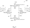
Fig. 5 illustrates a first alternative PCIe topology of the GPU system, according to one or more embodiments of the disclosure; -
Fig. 6 illustrates a second alternative PCIe topology of the GPU system, according to one or more embodiments of the disclosure; -
Fig. 7 illustrates a third alternative PCIe topology of the GPU system, according to one or more embodiments of the disclosure; -
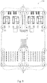
Fig. 8 is a top-down view of the PCIe baseboard, in accordance with an embodiment of the disclosure; -
Fig. 9A is a top-down view of a server GPU system, in accordance with an embodiment of the disclosure; and -
Fig. 9B is a top-down view of a desktop GPU system, in accordance with an embodiment of the disclosure. - The present invention is described with reference to the attached figures, where like reference numerals are used throughout the figures to designate similar or equivalent elements. The figures are not drawn to scale, and they are provided merely to illustrate the instant invention. Several aspects of the invention are described below with reference to example applications for illustration. It should be understood that numerous specific details, relationships, and methods are set forth to provide a full understanding of the invention. One having ordinary skill in the relevant art, however, will readily recognize that the invention can be practiced without one or more of the specific details, or with other methods. In other instances, well-known structures or operations are not shown in detail to avoid obscuring the invention. The present invention is not limited by the illustrated ordering of acts or events, as some acts may occur in different orders and/or concurrently with other acts or events. Furthermore, not all illustrated acts or events are required to implement a methodology in accordance with the present invention.
- In view of the foregoing, embodiments disclosed herein are directed to GPU systems that include a PCIe board configured to be selectively positioned in a first position or a second position. This type of PCIe board allows for the installation of GPU modules, such that any GPU fans in these GPU modules can be arranged to provide airflow in the same direction as the direction required for the electronics rack the GPU system in installed in. This is discussed in greater detail with respect to
Figs. 2A ,2B ,3A and3B . -
Fig. 2A is a top-down view of aserver GPU system 200A, in accordance with an embodiment of the disclosure. Theserver GPU system 200A has achassis 210, and thechassis 210 has afirst end 212 and asecond end 211. TheGPU system 200A has afront side 211 and aback side 212. In other words, thefirst end 212 corresponds to, e.g., is present at the same position of, theback side 212, while thesecond end 211 corresponds to, e.g., is present at the same position of, thefront side 211. Theserver GPU system 200A can have afront side 211 and arear side 212. Theserver GPU system 200A can include a first set ofGPU modules 215 and a second set ofGPU modules 216. In theserver GPU system 200A, the first and second sets ofGPU modules PCIe slots 217. Theserver GPU system 200A can also includefan modules 220 located opposite the first andsecond GPU modules fan modules 220 are located at thefirst end 212 of thechassis 210. Theserver GPU system 200A can also have aPCIe baseboard 218 andPDB 219. - As noted above, the
PCIe baseboard 218 can be installed in first and second positions. The first position in shown inFig. 2A . To support the multiple positions, thePCIe baseboard 218 andPDB 219 are connected using a cable methodology rather than using board-to-board connections. Therefore, as shown inFig. 2A , theserver GPU system 200A includespower cable connectors 31 connecting thePDB 219 with thefan modules 220, the first and second sets ofGPU modules PCIe slots 217. Each GPU module of the first and second sets ofGPU modules PCIe baseboard 218. ThePCIe slots 217 can also be connected to thePCIe baseboard 218 to facilitate connection between the received network cards and other server devices (not shown). ThePCIe slots 217 may separate thefirst GPU module 215 and thesecond GPU module 216, and thePCIe slot 217 is connected to at least onePCIe switch 224. In some embodiments, thePCIe baseboard 218 includes a plurality ofGPU slots GPU slot 221 is located in thefirst GPU module 215, while theGPU slot 222 is located in thesecond GPU module 216. -
Fig. 2B is a top-down view of adesktop GPU system 200B, in accordance with an embodiment of the disclosure. For any components inFig. 2B having the same reference numeral as inFig. 2A , the description inFig. 2A is sufficient for describing these components inFig. 2B unless otherwise indicated below. Indesktop GPU system 200B, thePCIe baseboard 218 is provided in a second position, i.e., rotated 180 degrees relative to its positon inFig. 2A . Thus, thePCIe baseboard 218 includes a printed circuit board (PCB) (not shown) design to support use thereof in the first or second positions. In some embodiments, the first set of theGPU module 215 includes aGPU fan 226, while the second set of theGPU module 216 includes aGPU fan 228. TheGPU slots PCIe baseboard 218 are used for installing a plurality of graphic processing units (GPUs) includingGPU fans - The
server GPU system 200A will keep the original GPU placement of theconventional GPU system 10. That is, the first and second sets ofGPU modules front side 211. In contrast, the rotation of thePCIe baseboard 218 will relocate the slots for the first and second sets ofGPU modules PDB 219. - In some embodiments, the board-to-board connector can include a P12V power connector and a sideband signal connector. In other embodiments, the
PDB 219 and thePCIe baseboard 218 can be connected using a cable methodology to allow for design flexibility. - The
server GPU system 200A and thedesktop GPU system 200B can route thepower cable connectors 31 in the center of thePCIe baseboard 218 to the center of thePDB 219. By routing thepower cable connectors 31 in the center of thePCIe baseboard 218, thepower cable connectors 31 are easier to service. Furthermore, routing thepower cable connectors 31 in the center of thePCIe baseboard 218 improves the performance of the plurality offan modules 220, but it may overlap with otherPCIe signal cables 32. If the cable is routed outside the center of thePCIe baseboard 218, the cable can block air flow. - Other configurations can include the
power cable connectors 31 being routed along the edges of thePCIe baseboard 218 to the edges of thePDB 219. These embodiments are discussed in greater detail with respect toFigs. 3A and3B . -
Fig. 3A is a top-down view of aserver GPU system 300A, in accordance with an embodiment of the disclosure. Theserver GPU system 300A is the same as theGPU system 200A except for alternative routing.Fig. 3B is a top-down view of adesktop GPU system 300B, in accordance with an embodiment of the disclosure. Thedesktop GPU system 300B is the same as thedesktop GPU system 200B except alternative routing. For any components inFigs. 3A and3B having the same reference numeral as inFig. 2A , the description inFig. 2A is sufficient for describing these components inFigs. 3A and3B unless otherwise indicated below. Theserver GPU system 300A and thedesktop GPU system 300B route thepower cable connectors 31 along the edges of thePCIe baseboard 218 to the edges of thePDB 219. By routing thepower cable connectors 31 along the edges of thePCIe baseboard 218 to the edges of thePDB 219, thepower cable connectors 31 can be separate from thePCIe signal cables 32. However, the routing of thepower cable connectors 31 along the edges of thePCIe baseboard 218 to the edges of thePDB 219 may negatively impact the performance of thefan modules 220. Furthermore, routing thepower cable connectors 31 along the edges of thePCIe baseboard 218 to the edges of thePDB 219 may make it difficult to service the cables since will be little space to uninstall the cables in order to service them. By routing thepower cable connectors 31 along the edges of thePCIe baseboard 218, more space is provided to place more components within the center of thePCIe baseboard 218. - In both the
server GPU system 300A and thedesktop GPU system 300B, thePCIe slots 217 are placed at the front side 211 (I/O side). However, the PCIe switch (not shown) has only one downstream port to connect to thePCIe slots 217. Because the PCIe switch has a limited PCIe lane, rotating the PCIe prevents the connection of the PCIe lane from the PCIe switch and the PCIe slot. To solve this issue, some embodiments of the disclosure implement an adaptor to switch between thedifferent PCIe slots 217. Specifically, a MUX switch can be implemented to switch to thedifferent PCIe slots 217. This is discussed in more detail with respect toFig. 5 . In alternative embodiments, a switched-capacitor resistor circuit can be connected to thePCIe slots 217. This is discussed in more detail with respect toFig. 6 . In additional alternative embodiments, a series of SlimSAS connectors can be implemented at the PCIe switches and thePCIe slots 217. This is discussed in more detail with respect toFig. 7 . In each of the embodiments discussed herein, space for thePCIe slots 217 is reserved at thefront side 211. -
Fig. 4 illustrates aPCIe topology 400 of the GPU system, according to one or more embodiments of the disclosure. ThePCIe topology 400 includes thePCIe slots 417 connected to a series of PCIe switches 418, 419, 420, and 421. ThePCIe slots 417 can include aleft PCIe slot 417A and aright PCIe slot 417B. Theleft PCIe slot 417A can be connected to thePCIe switch 418 by a PCIeinternal cable 401. Theleft PCIe slot 417A can also be connected to thePCIe switch 420 by a PCIeinternal cable 403. Theright PCIe slot 417B can be connected to thePCIe switch 419 by the PCIeinternal cable 402. Theright PCIe slot 417B can also be connected to thePCIe switch 421 by the PCIeinternal cable 404. - The series of PCIe switches 418, 419, 420, and 421 enable the
PCIe slots 417 to communicate with the first set of I/O ports 430 and the second set of I/O ports 431. The first set of I/O ports 430 are connected to the PCIe switches 418 and 419. The second set of I/O ports 431 are connected to the PCIe switches 420 and 421. The PCIe switches 418, 419, 420, and 421 facilitates the electrical connection between thePCIe slots 417 and the first and second set of I/O ports O ports PCIe slots 417 are directly connected to the series of PCIe switches 418, 419, 420, and 421 in an upstream manner, thePCIe slots 417 cannot be placed at the I/O side of the GPU system.Figs. 5-7 detail alternative topologies to be implemented in an embodiment of the present disclosure. -
Fig. 5 illustrates a firstalternative PCIe topology 500 of the GPU system, according to one or more embodiments of the disclosure. ThePCIe topology 500 includes afirst PCIe slot 517A and asecond PCIe slot 517B both connected to a series of PCIe switches 518 and 520 implementing multiplexers (MUX). The first andsecond PCIe slots PCIe switch 518 via afirst MUX 540. Specifically, thefirst PCIe slot 517A can be connected to thefirst MUX 540 by a PCIe trace onboard 501. Similarly, thesecond PCIe slot 517B can be connected to thefirst MUX 540 by a PCIe trace onboard 503. Thefirst MUX 540 can connect both the first andsecond PCIe slots PCIe switch 518 by a PCIe trace onboard 505. - Similarly, the first and
second PCIe slots PCIe switch 520 via asecond MUX 541. Specifically, thefirst PCIe slot 517A can be connected to thesecond MUX 541 by a PCIe trace onboard 502. Similarly, thesecond PCIe slot 517B can be connected to thesecond MUX 541 by a PCIe trace onboard 504. Thesecond MUX 541 can connect both the first andsecond PCIe slots PCIe switch 520 by a PCIe trace onboard 506. ThePCIe topology 500 economizes the connections between the first andsecond PCIe slots -
Fig. 6 illustrates a secondalternative PCIe topology 600 of the GPU system, according to one or more embodiments of the disclosure. ThePCIe topology 600 implements multiple switched-capacitor resistor circuits. The switched-capacitor resistor circuit is an electronic circuit element used for discrete-time signal processing. The switched-capacitor resistor circuit works by moving charges into and out of capacitors when switches are opened and closed. In the present embodiment, non-overlapping signals are used to control the switches, so that not all switches are closed simultaneously. - The
PCIe topology 600 includes afirst PCIe slot 617A and asecond PCIe slot 617B, both connected to a series of PCIe switches 618 and 620 implementing switched-capacitor resistor circuits. The first andsecond PCIe slots PCIe switch 618 via a first switched-capacitor resistor circuit 640. Specifically, thefirst PCIe slot 617A can be connected to the first switched-capacitor resistor circuit 640 by a PCIe trace onboard 601. Similarly, thesecond PCIe slot 617B can be connected to the first switched-capacitor resistor circuit 640 by a PCIe trace onboard 603. The first switched-capacitor resistor circuit 640 can connect both the first andsecond PCIe slots PCIe switch 618 by a PCIe trace onboard 605. The first switched-capacitor resistor circuit 640 can be made up of one a first capacitor C1 and a second capacitor C2, which are overlapped to alternate the input and output of the first switched-capacitor resistor circuit 640. - Similarly, the first and
second PCIe slots PCIe switch 620 via a second switched-capacitor resistor circuit 641. Specifically, thefirst PCIe slot 617A can be connected to the second switched-capacitor resistor circuit 641 by a PCIe trace onboard 602. Similarly, thesecond PCIe slot 617B can be connected to the second switched-capacitor resistor circuit 641 by a PCIe trace onboard 604. The second switched-capacitor resistor circuit 641 can connect both the first andsecond PCIe slots PCIe switch 620 by a PCIe trace onboard 606. The second switched-capacitor resistor circuit 641 can be made up of a first capacitor C1 and a second capacitor C2, which are overlapped to alternate the input and output of the second switched-capacitor resistor circuit 641. -
Fig. 7 illustrates a thirdalternative PCIe topology 700 of the GPU system, according to one or more embodiments of the disclosure. ThePCIe topology 700 implements multiple high speed connectors. In some embodiments, the high-speed connectors can be SlimSAS connectors. The high-speed connectors enable designers to achieve high port density, configurability, and utilization. Their design provides mechanical durability and resonance dampening features. The SlimSAS connectors can be connected by SlimSAS cables, which are configured to address various interconnect issues such as bulk cable form factor restrictions. - The
PCIe topology 700 includes afirst PCIe slot 717A and asecond PCIe slot 717B, both connected to a series of PCIe switches 718 and 720 implementing high-speed connectors such as SlimSAS connectors. The first andsecond PCIe slots PCIe switch 718 via a first switch-SlimSAS connector 740. Specifically, thefirst PCIe slot 717A can be connected to afirst SlimSAS connector 739 by a PCIe trace onboard 701. Thefirst SlimSAS connector 739 and the first switch-SlimSAS connector 740 can be connected by a high-speed cable 705. In some embodiments, the high-speed cable 705 can be a SlimSAS cable. - Similarly, the
second PCIe slot 717B can be connected to asecond SlimSAS connector 738 by a PCIe trace onboard 703. Thesecond SlimSAS connector 738 and the first switch-SlimSAS connector 740 can be connected by a high-speed cable 707. In some embodiments, the high-speed cable 707 can be a SlimSAS cable. The first switch-SlimSAS connector 740 can be connected to thePCIe switch 718 by a PCIe trace onboard 709. In other words, thefirst PCIe slot 717A and asecond PCIe slot 717B can both connected to thePCIe switch 718 via the series of SlimSAS connectors. - The first and
second PCIe slots PCIe switch 720 via a second switch-SlimSAS connector 741. Specifically, thefirst PCIe slot 717A can be connected to athird SlimSAS connector 737 by a PCIe trace onboard 702. Thethird SlimSAS connector 737 and the second switch-SlimSAS connector 741 can be connected by a high-speed cable 706. In some embodiments, the high-speed cable 706 can be a SlimSAS cable. - Similarly, the
second PCIe slot 717B can be connected to afourth SlimSAS connector 736 by a PCIe trace onboard 704. Thefourth SlimSAS connector 736 and the second switch-SlimSAS connector 741 can be connected by a high-speed cable 708. In some embodiments, the high-speed cable 708 can be a SlimSAS cable. The second switch-SlimSAS connector 741 can be connected to thePCIe switch 720 by a PCIe trace onboard 710. In other words, thefirst PCIe slot 717A and asecond PCIe slot 717B can both connected to thePCIe switch 720 via the series of SlimSAS connectors. The series of SlimSAS connectors and associated SlimSAS cables can enable switching between the first andsecond PCIe slots - Referring momentarily back to
Figs. 2A and2B , the length of thePCIe signal cables 32 will vary in theserver GPU system 200A and thedesktop GPU system 200B embodiments. Upon rotating thePCIe baseboard 218 to create thedesktop GPU system 200B, the length of thePCIe signal cables 32 is shortened, thereby improving the signal integrity. In the embodiment ofPCIe topology 700, thePCIe signal cables 32 can be miniSAS cables. Rotating thePCIe baseboard 218 to create thedesktop GPU system 200B can require various mechanical embodiments of theserver GPU system 200A. This is discussed in greater detail below with respect toFigs. 9A and9B . -
Fig. 8 is a top-down view of thePCIe baseboard 818 implemented in thedesktop GPU system 300B and theserver GPU system 300A. The screw mounting holes H can be located at different locations on thePCIe baseboard 818 to create a symmetrical layout. The screw mounting holes H can assist the rotation and placement of thePCIe baseboard 818. In addition to screw mounting holes H, bracket assemblies also facilitate the 180-degree rotation of thePCIe baseboard 818. This is discussed in more detail with respect toFigs. 9A and9B . -
Fig. 9A andFig. 9B are perspective views of aserver GPU system 900A and adesktop GPU system 900B, respectively, in accordance with an embodiment of the disclosure. Theserver GPU system 900A includes afirst GPU bracket 901 and asecond GPU bracket 904. Each GPU card can be fixed by two brackets in its rear and front side for stability. For example, theGPU brackets GPU system 900A. In comparison, thedesktop GPU system 900B includes afirst GPU bracket 902 and asecond GPU bracket 903. In the process of rotating thePCIe baseboard 918, the first and second plurality ofGPU modules rear side 912 of thedesktop GPU system 900B. Thefirst GPU bracket 902 is implemented to separate thePCIe baseboard 918 from the PDB (not shown) that would be positioned just above thePCIe baseboard 918. The desktop GPU modules are fixed bybracket 902 andbracket 903 of 900B system where thePCIe baseboard 918 is reversed. In some embodiments of theGPU system 900B, theGPU bracket 904 ofGPU system 900A is still implemented although it is no longer supporting the GPU modules. - The terminology used herein is for the purpose of describing particular embodiments only and is not intended to limit the invention. As used herein, the singular forms "a," "an," and "the" are intended to include the plural forms as well, unless the context clearly indicates otherwise. Furthermore, to the extent that the terms "including," "includes," "having," "has," "with," or variants thereof are used in either the detailed description and/or the claims, such terms are intended to be inclusive in a manner similar to the term "comprising."
- Unless otherwise defined, all terms (including technical and scientific terms) used herein have the same meaning as commonly understood by one of ordinary skill in the art to which this invention belongs. Furthermore, terms, such as those defined in commonly used dictionaries, should be interpreted as having a meaning that is consistent with their meaning in the context of the relevant art, and will not be interpreted in an idealized or overly formal sense unless expressly so defined herein.
- Although particular embodiments have been described herein, it will be appreciated that the invention is not limited thereto and that many modifications and additions thereto may be made within the scope of the invention. For example, various combinations of the features of the following dependent claims can be made with the features of the independent claims without departing from the scope of the present invention.
Claims (11)
- A computing device, characterized by:a chassis (210) with a first end (212) and a second end (211);a plurality of fan modules (220) located at the first end (212) of the chassis (210); anda Peripheral Component Interconnect Express (PCIe) baseboard (218) located at a front side (211) of the chassis (210), the PCIe baseboard (218) configured to support placement thereof in the chassis (210) in a first position and a second position,wherein the second position of the PCIe baseboard (218) is a 180-degree rotation from the first position, and wherein the PCIe baseboard (218) comprises a plurality of GPU slots (221, 222) for installing a plurality of graphic processing units (GPUs) (215, 216) comprising GPU fans (226, 228).
- The computing device of claim 1, further comprising a power distribution board (PDB) (219) housed between the plurality of fan modules (220) and the PCIe baseboard (218).
- The computing device of claim 2, wherein the PCIe baseboard further comprises at least one PCIe slot (217) separating a plurality of first and second GPUs of the GPUs (215, 216), wherein the at least one PCIe slot (217) is connected to at least one PCIe switch (224).
- The computing device of claim 3, further comprising power cable connectors (31) connecting the PDB (219) with the plurality of GPU fans (226, 228), the first and second plurality of graphic processing units (215, 216), and the at least one PCIe slot (217).
- The computing device of claim 4, wherein the power cable connectors (31) can be routed towards a center line of the PCIe baseboard (218) or along outer edges of the PCIe baseboard (218).
- The computing device of any of claims 3-5, further comprising PCIe signal cables (32) connecting the at least one PCIe slot (217) to the at least one PCIe switch (224).
- The computing device of claim 6, wherein the PCIe signal cables (32) are shorter in the second position of the PCIe baseboard (218) than in the first position of the PCIe baseboard (218).
- The computing device of any of claims 1-7, wherein at least two PCIe slots (517A, 517B) are connected to the at least one PCIe switch (518) via at least one of: a MUX switch, a switched-capacitor resistor circuit, and/or a SlimSAS connector.
- The computing device of any of claims 1-8, wherein the first position of the PCIe baseboard (218) is a server GPU configuration, wherein the at least one PCIe switch (224) is located between the first and second plurality of graphic processing units (215, 216) and the plurality of fan modules (220).
- The computing device of any of claims 1-9, wherein the second position of the PCIe baseboard (218) is a desktop GPU configuration, wherein the at least one PCIe switch (224) is located at the front side (211) of the chassis (210).
- The computing device of any of claims 1-10, wherein the PCIe baseboard comprises a plurality of screw mounting holes (H) symmetrically positioned on the PCIe baseboard (818) to enable a transition between the first position and the second position.
Applications Claiming Priority (1)
| Application Number | Priority Date | Filing Date | Title |
|---|---|---|---|
| US16/124,345 US10595444B1 (en) | 2018-09-07 | 2018-09-07 | Rotatable board configuration to improve cooling |
Publications (2)
| Publication Number | Publication Date |
|---|---|
| EP3620892A1 true EP3620892A1 (en) | 2020-03-11 |
| EP3620892B1 EP3620892B1 (en) | 2022-05-11 |
Family
ID=65766914
Family Applications (1)
| Application Number | Title | Priority Date | Filing Date |
|---|---|---|---|
| EP19162172.1A Active EP3620892B1 (en) | 2018-09-07 | 2019-03-12 | Rotatable board configuration to improve cooling |
Country Status (5)
| Country | Link |
|---|---|
| US (1) | US10595444B1 (en) |
| EP (1) | EP3620892B1 (en) |
| JP (1) | JP6754461B2 (en) |
| CN (1) | CN110888498B (en) |
| TW (1) | TWI676885B (en) |
Cited By (2)
| Publication number | Priority date | Publication date | Assignee | Title |
|---|---|---|---|---|
| CN111966175A (en) * | 2020-08-14 | 2020-11-20 | 苏州浪潮智能科技有限公司 | A kind of GPU fixing structure and installation method thereof |
| CN115023071A (en) * | 2021-03-05 | 2022-09-06 | 百度(美国)有限责任公司 | Rotary power delivery module for server |
Families Citing this family (3)
| Publication number | Priority date | Publication date | Assignee | Title |
|---|---|---|---|---|
| US12471238B2 (en) * | 2021-01-22 | 2025-11-11 | Nvidia Corporation | Static data center power balancing and configuration |
| US20230418345A1 (en) * | 2022-06-22 | 2023-12-28 | Jose Augusto Vullo | Disposal of refrigeration applied in machines or equipment or kits for mining cryptocurrencies and/or for data processing |
| TWI883633B (en) * | 2023-11-08 | 2025-05-11 | 英業達股份有限公司 | Gpu module |
Citations (4)
| Publication number | Priority date | Publication date | Assignee | Title |
|---|---|---|---|---|
| US20140211410A1 (en) * | 2013-01-28 | 2014-07-31 | Origin Pc | Configurable computer housing |
| US20160154765A1 (en) * | 2014-12-01 | 2016-06-02 | Sk Hynix Memory Solutions Inc. | Storage node based on pci express interface |
| CN104657317B (en) * | 2015-03-06 | 2017-12-26 | 北京百度网讯科技有限公司 | Server |
| US9870333B1 (en) * | 2014-09-12 | 2018-01-16 | Keysight Technologies, Inc. | Instrumentation chassis including integrated accelerator module |
Family Cites Families (11)
| Publication number | Priority date | Publication date | Assignee | Title |
|---|---|---|---|---|
| EP1532852A1 (en) * | 2002-05-31 | 2005-05-25 | Verari Systems, Inc. | Methods and apparatus for mounting computer components |
| US7382616B2 (en) * | 2005-01-21 | 2008-06-03 | Nvidia Corporation | Cooling system for computer hardware |
| JP2010251620A (en) | 2009-04-17 | 2010-11-04 | Sony Corp | Electronics |
| US9144179B2 (en) * | 2013-02-01 | 2015-09-22 | Dell Products, L.P. | System and method for powering multiple electronic devices operating within an immersion cooling vessel |
| US9582366B2 (en) * | 2014-11-21 | 2017-02-28 | International Business Machines Corporation | Detecting and sparing of optical PCIE cable channel attached IO drawer |
| JP6410042B2 (en) * | 2014-12-25 | 2018-10-24 | キヤノンファインテックニスカ株式会社 | Image reading device |
| US9807901B2 (en) * | 2015-03-06 | 2017-10-31 | Facebook, Inc. | Multiple graphics processing unit platform |
| US20170262029A1 (en) * | 2016-03-14 | 2017-09-14 | Intel Corporation | Data storage system with parallel array of dense memory cards and high airflow |
| US10387346B2 (en) * | 2016-05-06 | 2019-08-20 | Quanta Computer Inc. | Dynamic PCIE switch reconfiguration mechanism |
| US10356934B2 (en) * | 2016-09-30 | 2019-07-16 | Quanta Computer Inc. | Server rack system and bidirectional power inlet |
| JP3213991U (en) * | 2017-09-29 | 2017-12-14 | 株式会社セガゲームス | Computer equipment |
-
2018
- 2018-09-07 US US16/124,345 patent/US10595444B1/en active Active
- 2018-12-10 TW TW107144381A patent/TWI676885B/en active
- 2018-12-28 CN CN201811654128.4A patent/CN110888498B/en active Active
-
2019
- 2019-03-12 EP EP19162172.1A patent/EP3620892B1/en active Active
- 2019-03-22 JP JP2019055340A patent/JP6754461B2/en active Active
Patent Citations (4)
| Publication number | Priority date | Publication date | Assignee | Title |
|---|---|---|---|---|
| US20140211410A1 (en) * | 2013-01-28 | 2014-07-31 | Origin Pc | Configurable computer housing |
| US9870333B1 (en) * | 2014-09-12 | 2018-01-16 | Keysight Technologies, Inc. | Instrumentation chassis including integrated accelerator module |
| US20160154765A1 (en) * | 2014-12-01 | 2016-06-02 | Sk Hynix Memory Solutions Inc. | Storage node based on pci express interface |
| CN104657317B (en) * | 2015-03-06 | 2017-12-26 | 北京百度网讯科技有限公司 | Server |
Cited By (3)
| Publication number | Priority date | Publication date | Assignee | Title |
|---|---|---|---|---|
| CN111966175A (en) * | 2020-08-14 | 2020-11-20 | 苏州浪潮智能科技有限公司 | A kind of GPU fixing structure and installation method thereof |
| CN115023071A (en) * | 2021-03-05 | 2022-09-06 | 百度(美国)有限责任公司 | Rotary power delivery module for server |
| CN115023071B (en) * | 2021-03-05 | 2025-01-10 | 百度(美国)有限责任公司 | Rotary power delivery module for server |
Also Published As
| Publication number | Publication date |
|---|---|
| JP2020042763A (en) | 2020-03-19 |
| US10595444B1 (en) | 2020-03-17 |
| JP6754461B2 (en) | 2020-09-09 |
| US20200084919A1 (en) | 2020-03-12 |
| EP3620892B1 (en) | 2022-05-11 |
| TWI676885B (en) | 2019-11-11 |
| TW202011148A (en) | 2020-03-16 |
| CN110888498A (en) | 2020-03-17 |
| CN110888498B (en) | 2021-08-13 |
Similar Documents
| Publication | Publication Date | Title |
|---|---|---|
| EP3620892B1 (en) | Rotatable board configuration to improve cooling | |
| US20030112582A1 (en) | Redundant data and power infrastructure for modular server components in a rack | |
| CA2621286C (en) | Avionics equipment carrier system with quick-mount housing and quick-mount modules | |
| US6805560B1 (en) | Apparatus interconnecting circuit board and mezzanine card or cards | |
| US7764511B2 (en) | Multidirectional configurable architecture for multi-processor system | |
| EP2941107B1 (en) | Heat dissipation system for communication device | |
| US10925167B2 (en) | Modular expansion card bus | |
| US20080043405A1 (en) | Chassis partition architecture for multi-processor system | |
| WO2008067188A1 (en) | Method and system for switchless backplane controller using existing standards-based backplanes | |
| CN102866729B (en) | Server cabinet system | |
| TWI603202B (en) | Apparatuses and systems with redirection of lane resources | |
| US8358511B2 (en) | Electronic board arrangement and electronic interconnect board of an electronic board arrangement | |
| EP1994809A2 (en) | Configurable chassis guidance system | |
| US6608761B2 (en) | Multiple processor cards accessing common peripherals via transparent and non-transparent bridges | |
| US20090228628A1 (en) | Multi-fpga pci express x16 architecture | |
| EP2140741B1 (en) | A printed board assembly and a method | |
| CN105027518A (en) | Interconnection system for communications device | |
| US7136290B1 (en) | Blade circuit cross-connection adapted for peer-to-peer backplanes | |
| EP1415234B1 (en) | High density severlets utilizing high speed data bus | |
| CN206258768U (en) | cabinet system | |
| US9384104B2 (en) | Testing a processor assembly | |
| CN106445001A (en) | Running state information sharing server system | |
| HK1062718B (en) | High density serverlets utilizing high speed data bus | |
| CN104571331A (en) | Electronic device | |
| JPH10268977A (en) | Signal connecting method between cards and plural substrate connecting structure |
Legal Events
| Date | Code | Title | Description |
|---|---|---|---|
| PUAI | Public reference made under article 153(3) epc to a published international application that has entered the european phase |
Free format text: ORIGINAL CODE: 0009012 |
|
| STAA | Information on the status of an ep patent application or granted ep patent |
Free format text: STATUS: THE APPLICATION HAS BEEN PUBLISHED |
|
| AK | Designated contracting states |
Kind code of ref document: A1 Designated state(s): AL AT BE BG CH CY CZ DE DK EE ES FI FR GB GR HR HU IE IS IT LI LT LU LV MC MK MT NL NO PL PT RO RS SE SI SK SM TR |
|
| AX | Request for extension of the european patent |
Extension state: BA ME |
|
| STAA | Information on the status of an ep patent application or granted ep patent |
Free format text: STATUS: REQUEST FOR EXAMINATION WAS MADE |
|
| 17P | Request for examination filed |
Effective date: 20200613 |
|
| RBV | Designated contracting states (corrected) |
Designated state(s): AL AT BE BG CH CY CZ DE DK EE ES FI FR GB GR HR HU IE IS IT LI LT LU LV MC MK MT NL NO PL PT RO RS SE SI SK SM TR |
|
| RIC1 | Information provided on ipc code assigned before grant |
Ipc: H05K 7/20 20060101ALI20211029BHEP Ipc: H05K 7/14 20060101ALI20211029BHEP Ipc: G06F 1/20 20060101ALI20211029BHEP Ipc: G06F 1/18 20060101AFI20211029BHEP |
|
| GRAP | Despatch of communication of intention to grant a patent |
Free format text: ORIGINAL CODE: EPIDOSNIGR1 |
|
| STAA | Information on the status of an ep patent application or granted ep patent |
Free format text: STATUS: GRANT OF PATENT IS INTENDED |
|
| INTG | Intention to grant announced |
Effective date: 20211220 |
|
| GRAS | Grant fee paid |
Free format text: ORIGINAL CODE: EPIDOSNIGR3 |
|
| GRAA | (expected) grant |
Free format text: ORIGINAL CODE: 0009210 |
|
| STAA | Information on the status of an ep patent application or granted ep patent |
Free format text: STATUS: THE PATENT HAS BEEN GRANTED |
|
| AK | Designated contracting states |
Kind code of ref document: B1 Designated state(s): AL AT BE BG CH CY CZ DE DK EE ES FI FR GB GR HR HU IE IS IT LI LT LU LV MC MK MT NL NO PL PT RO RS SE SI SK SM TR |
|
| REG | Reference to a national code |
Ref country code: GB Ref legal event code: FG4D |
|
| REG | Reference to a national code |
Ref country code: CH Ref legal event code: EP |
|
| REG | Reference to a national code |
Ref country code: AT Ref legal event code: REF Ref document number: 1491990 Country of ref document: AT Kind code of ref document: T Effective date: 20220515 |
|
| REG | Reference to a national code |
Ref country code: DE Ref legal event code: R096 Ref document number: 602019014722 Country of ref document: DE |
|
| REG | Reference to a national code |
Ref country code: IE Ref legal event code: FG4D |
|
| REG | Reference to a national code |
Ref country code: LT Ref legal event code: MG9D |
|
| REG | Reference to a national code |
Ref country code: NL Ref legal event code: MP Effective date: 20220511 |
|
| REG | Reference to a national code |
Ref country code: AT Ref legal event code: MK05 Ref document number: 1491990 Country of ref document: AT Kind code of ref document: T Effective date: 20220511 |
|
| PG25 | Lapsed in a contracting state [announced via postgrant information from national office to epo] |
Ref country code: SE Free format text: LAPSE BECAUSE OF FAILURE TO SUBMIT A TRANSLATION OF THE DESCRIPTION OR TO PAY THE FEE WITHIN THE PRESCRIBED TIME-LIMIT Effective date: 20220511 Ref country code: PT Free format text: LAPSE BECAUSE OF FAILURE TO SUBMIT A TRANSLATION OF THE DESCRIPTION OR TO PAY THE FEE WITHIN THE PRESCRIBED TIME-LIMIT Effective date: 20220912 Ref country code: NO Free format text: LAPSE BECAUSE OF FAILURE TO SUBMIT A TRANSLATION OF THE DESCRIPTION OR TO PAY THE FEE WITHIN THE PRESCRIBED TIME-LIMIT Effective date: 20220811 Ref country code: NL Free format text: LAPSE BECAUSE OF FAILURE TO SUBMIT A TRANSLATION OF THE DESCRIPTION OR TO PAY THE FEE WITHIN THE PRESCRIBED TIME-LIMIT Effective date: 20220511 Ref country code: LT Free format text: LAPSE BECAUSE OF FAILURE TO SUBMIT A TRANSLATION OF THE DESCRIPTION OR TO PAY THE FEE WITHIN THE PRESCRIBED TIME-LIMIT Effective date: 20220511 Ref country code: HR Free format text: LAPSE BECAUSE OF FAILURE TO SUBMIT A TRANSLATION OF THE DESCRIPTION OR TO PAY THE FEE WITHIN THE PRESCRIBED TIME-LIMIT Effective date: 20220511 Ref country code: GR Free format text: LAPSE BECAUSE OF FAILURE TO SUBMIT A TRANSLATION OF THE DESCRIPTION OR TO PAY THE FEE WITHIN THE PRESCRIBED TIME-LIMIT Effective date: 20220812 Ref country code: FI Free format text: LAPSE BECAUSE OF FAILURE TO SUBMIT A TRANSLATION OF THE DESCRIPTION OR TO PAY THE FEE WITHIN THE PRESCRIBED TIME-LIMIT Effective date: 20220511 Ref country code: ES Free format text: LAPSE BECAUSE OF FAILURE TO SUBMIT A TRANSLATION OF THE DESCRIPTION OR TO PAY THE FEE WITHIN THE PRESCRIBED TIME-LIMIT Effective date: 20220511 Ref country code: BG Free format text: LAPSE BECAUSE OF FAILURE TO SUBMIT A TRANSLATION OF THE DESCRIPTION OR TO PAY THE FEE WITHIN THE PRESCRIBED TIME-LIMIT Effective date: 20220811 Ref country code: AT Free format text: LAPSE BECAUSE OF FAILURE TO SUBMIT A TRANSLATION OF THE DESCRIPTION OR TO PAY THE FEE WITHIN THE PRESCRIBED TIME-LIMIT Effective date: 20220511 |
|
| PG25 | Lapsed in a contracting state [announced via postgrant information from national office to epo] |
Ref country code: RS Free format text: LAPSE BECAUSE OF FAILURE TO SUBMIT A TRANSLATION OF THE DESCRIPTION OR TO PAY THE FEE WITHIN THE PRESCRIBED TIME-LIMIT Effective date: 20220511 Ref country code: PL Free format text: LAPSE BECAUSE OF FAILURE TO SUBMIT A TRANSLATION OF THE DESCRIPTION OR TO PAY THE FEE WITHIN THE PRESCRIBED TIME-LIMIT Effective date: 20220511 Ref country code: LV Free format text: LAPSE BECAUSE OF FAILURE TO SUBMIT A TRANSLATION OF THE DESCRIPTION OR TO PAY THE FEE WITHIN THE PRESCRIBED TIME-LIMIT Effective date: 20220511 Ref country code: IS Free format text: LAPSE BECAUSE OF FAILURE TO SUBMIT A TRANSLATION OF THE DESCRIPTION OR TO PAY THE FEE WITHIN THE PRESCRIBED TIME-LIMIT Effective date: 20220911 |
|
| PG25 | Lapsed in a contracting state [announced via postgrant information from national office to epo] |
Ref country code: SM Free format text: LAPSE BECAUSE OF FAILURE TO SUBMIT A TRANSLATION OF THE DESCRIPTION OR TO PAY THE FEE WITHIN THE PRESCRIBED TIME-LIMIT Effective date: 20220511 Ref country code: SK Free format text: LAPSE BECAUSE OF FAILURE TO SUBMIT A TRANSLATION OF THE DESCRIPTION OR TO PAY THE FEE WITHIN THE PRESCRIBED TIME-LIMIT Effective date: 20220511 Ref country code: RO Free format text: LAPSE BECAUSE OF FAILURE TO SUBMIT A TRANSLATION OF THE DESCRIPTION OR TO PAY THE FEE WITHIN THE PRESCRIBED TIME-LIMIT Effective date: 20220511 Ref country code: EE Free format text: LAPSE BECAUSE OF FAILURE TO SUBMIT A TRANSLATION OF THE DESCRIPTION OR TO PAY THE FEE WITHIN THE PRESCRIBED TIME-LIMIT Effective date: 20220511 Ref country code: DK Free format text: LAPSE BECAUSE OF FAILURE TO SUBMIT A TRANSLATION OF THE DESCRIPTION OR TO PAY THE FEE WITHIN THE PRESCRIBED TIME-LIMIT Effective date: 20220511 Ref country code: CZ Free format text: LAPSE BECAUSE OF FAILURE TO SUBMIT A TRANSLATION OF THE DESCRIPTION OR TO PAY THE FEE WITHIN THE PRESCRIBED TIME-LIMIT Effective date: 20220511 |
|
| REG | Reference to a national code |
Ref country code: DE Ref legal event code: R097 Ref document number: 602019014722 Country of ref document: DE |
|
| PLBE | No opposition filed within time limit |
Free format text: ORIGINAL CODE: 0009261 |
|
| STAA | Information on the status of an ep patent application or granted ep patent |
Free format text: STATUS: NO OPPOSITION FILED WITHIN TIME LIMIT |
|
| PG25 | Lapsed in a contracting state [announced via postgrant information from national office to epo] |
Ref country code: AL Free format text: LAPSE BECAUSE OF FAILURE TO SUBMIT A TRANSLATION OF THE DESCRIPTION OR TO PAY THE FEE WITHIN THE PRESCRIBED TIME-LIMIT Effective date: 20220511 |
|
| 26N | No opposition filed |
Effective date: 20230214 |
|
| PG25 | Lapsed in a contracting state [announced via postgrant information from national office to epo] |
Ref country code: SI Free format text: LAPSE BECAUSE OF FAILURE TO SUBMIT A TRANSLATION OF THE DESCRIPTION OR TO PAY THE FEE WITHIN THE PRESCRIBED TIME-LIMIT Effective date: 20220511 |
|
| PG25 | Lapsed in a contracting state [announced via postgrant information from national office to epo] |
Ref country code: MC Free format text: LAPSE BECAUSE OF FAILURE TO SUBMIT A TRANSLATION OF THE DESCRIPTION OR TO PAY THE FEE WITHIN THE PRESCRIBED TIME-LIMIT Effective date: 20220511 |
|
| REG | Reference to a national code |
Ref country code: CH Ref legal event code: PL |
|
| REG | Reference to a national code |
Ref country code: BE Ref legal event code: MM Effective date: 20230331 |
|
| PG25 | Lapsed in a contracting state [announced via postgrant information from national office to epo] |
Ref country code: LU Free format text: LAPSE BECAUSE OF NON-PAYMENT OF DUE FEES Effective date: 20230312 |
|
| REG | Reference to a national code |
Ref country code: IE Ref legal event code: MM4A |
|
| PG25 | Lapsed in a contracting state [announced via postgrant information from national office to epo] |
Ref country code: LI Free format text: LAPSE BECAUSE OF NON-PAYMENT OF DUE FEES Effective date: 20230331 Ref country code: IT Free format text: LAPSE BECAUSE OF FAILURE TO SUBMIT A TRANSLATION OF THE DESCRIPTION OR TO PAY THE FEE WITHIN THE PRESCRIBED TIME-LIMIT Effective date: 20220511 Ref country code: IE Free format text: LAPSE BECAUSE OF NON-PAYMENT OF DUE FEES Effective date: 20230312 Ref country code: CH Free format text: LAPSE BECAUSE OF NON-PAYMENT OF DUE FEES Effective date: 20230331 |
|
| PG25 | Lapsed in a contracting state [announced via postgrant information from national office to epo] |
Ref country code: BE Free format text: LAPSE BECAUSE OF NON-PAYMENT OF DUE FEES Effective date: 20230331 |
|
| PG25 | Lapsed in a contracting state [announced via postgrant information from national office to epo] |
Ref country code: BG Free format text: LAPSE BECAUSE OF FAILURE TO SUBMIT A TRANSLATION OF THE DESCRIPTION OR TO PAY THE FEE WITHIN THE PRESCRIBED TIME-LIMIT Effective date: 20220511 |
|
| PG25 | Lapsed in a contracting state [announced via postgrant information from national office to epo] |
Ref country code: BG Free format text: LAPSE BECAUSE OF FAILURE TO SUBMIT A TRANSLATION OF THE DESCRIPTION OR TO PAY THE FEE WITHIN THE PRESCRIBED TIME-LIMIT Effective date: 20220511 |
|
| PG25 | Lapsed in a contracting state [announced via postgrant information from national office to epo] |
Ref country code: CY Free format text: LAPSE BECAUSE OF FAILURE TO SUBMIT A TRANSLATION OF THE DESCRIPTION OR TO PAY THE FEE WITHIN THE PRESCRIBED TIME-LIMIT; INVALID AB INITIO Effective date: 20190312 |
|
| PG25 | Lapsed in a contracting state [announced via postgrant information from national office to epo] |
Ref country code: HU Free format text: LAPSE BECAUSE OF FAILURE TO SUBMIT A TRANSLATION OF THE DESCRIPTION OR TO PAY THE FEE WITHIN THE PRESCRIBED TIME-LIMIT; INVALID AB INITIO Effective date: 20190312 |
|
| PG25 | Lapsed in a contracting state [announced via postgrant information from national office to epo] |
Ref country code: TR Free format text: LAPSE BECAUSE OF FAILURE TO SUBMIT A TRANSLATION OF THE DESCRIPTION OR TO PAY THE FEE WITHIN THE PRESCRIBED TIME-LIMIT Effective date: 20220511 |
|
| PGFP | Annual fee paid to national office [announced via postgrant information from national office to epo] |
Ref country code: GB Payment date: 20260128 Year of fee payment: 8 |
|
| PGFP | Annual fee paid to national office [announced via postgrant information from national office to epo] |
Ref country code: DE Payment date: 20260121 Year of fee payment: 8 |
|
| PGFP | Annual fee paid to national office [announced via postgrant information from national office to epo] |
Ref country code: FR Payment date: 20260121 Year of fee payment: 8 |