EP3620783A1 - Field-effect transistor-based biosensor - Google Patents
Field-effect transistor-based biosensor Download PDFInfo
- Publication number
- EP3620783A1 EP3620783A1 EP18192768.2A EP18192768A EP3620783A1 EP 3620783 A1 EP3620783 A1 EP 3620783A1 EP 18192768 A EP18192768 A EP 18192768A EP 3620783 A1 EP3620783 A1 EP 3620783A1
- Authority
- EP
- European Patent Office
- Prior art keywords
- zone
- region
- sensor
- channel region
- top surface
- Prior art date
- Legal status (The legal status is an assumption and is not a legal conclusion. Google has not performed a legal analysis and makes no representation as to the accuracy of the status listed.)
- Granted
Links
Images





Classifications
-
- G—PHYSICS
- G01—MEASURING; TESTING
- G01N—INVESTIGATING OR ANALYSING MATERIALS BY DETERMINING THEIR CHEMICAL OR PHYSICAL PROPERTIES
- G01N27/00—Investigating or analysing materials by the use of electric, electrochemical, or magnetic means
- G01N27/26—Investigating or analysing materials by the use of electric, electrochemical, or magnetic means by investigating electrochemical variables; by using electrolysis or electrophoresis
- G01N27/403—Cells and electrode assemblies
- G01N27/414—Ion-sensitive or chemical field-effect transistors, i.e. ISFETS or CHEMFETS
- G01N27/4145—Ion-sensitive or chemical field-effect transistors, i.e. ISFETS or CHEMFETS specially adapted for biomolecules, e.g. gate electrode with immobilised receptors
-
- B—PERFORMING OPERATIONS; TRANSPORTING
- B82—NANOTECHNOLOGY
- B82Y—SPECIFIC USES OR APPLICATIONS OF NANOSTRUCTURES; MEASUREMENT OR ANALYSIS OF NANOSTRUCTURES; MANUFACTURE OR TREATMENT OF NANOSTRUCTURES
- B82Y15/00—Nanotechnology for interacting, sensing or actuating, e.g. quantum dots as markers in protein assays or molecular motors
Definitions
- the present invention relates to the field of Field-effect transistor-based biosensors (bioFETs) and to method of making and using the same.
- BioFETs sense molecules as charge or dielectric displacements close to their gate dielectric. These transistors do not have their solid gate electrode directly in contact with the gate dielectric. Instead, they have a liquid electrolyte gate in contact with the gate dielectric and the solid gate electrode is in electrical contact with the liquid electrolyte gate. The sensed molecules are located in this liquid gate at or near the gate dielectric surface. The molecular charge or dielectric displacement near the gate dielectric causes a change in the current running through the semiconductor channel of the device as dictated by the disturbance in the electrical potential landscape these molecules cause. Such devices are currently considered promising for single molecule detection and highly sensitive molecular detection.
- One of the main contemporary obstacles inhibiting the effectivity of such single molecule and highly sensitive FET devices is the weak signal a single electronic charge / molecule generates for FET devices of a size currently deemed manufacturable in top-down semiconductor manufacturing technologies.
- One key cause of the weak signal is the screening of molecular charges by the electrolyte.
- the salt concentration has to be near physiological levels which introduces significant screening.
- the physiological NaCI concentration is 154mM at which the Debye length becomes smaller than 1nm.
- salinity can be lowered but screening remains a central issue.
- a second key issue is bio-fouling which originates from non-target molecules which bind to the FET sensor and cause false signals.
- sensors according to embodiments of the present invention have a good sensitivity. For instance, in some embodiments, single molecules can be detected.
- sensors according to embodiments of the present invention have high selectivity or specificity. Indeed, they are not very impacted by fouling.
- sensors according to embodiments of the present invention are relatively inexpensive to produce.
- An alternative way to increase sensitivity would be to shorten the channel length by shortening the distance between the source region and the drain region but the smaller this distance, the more difficult it becomes to form steep doping profiles for the source and drain, hence raising the costs.
- Embodiments of the present invention permit to obtain the sensitivity of a shorter such distance without having to actually shorten that distance.
- the present invention relates to a sensor.
- the sensor comprises a field effect transistor.
- the field effect transistor comprises an active region.
- the active region comprises a source region and a drain region defining a source-drain axis.
- the active region further comprises a channel region between the source region and the drain region.
- the field effect transistor further comprises a dielectric region. This dielectric region is on the channel region.
- This dielectric region comprises at least a first zone on a first portion of the channel region and a second zone on a second portion of the channel region.
- the first zone measures from 1 to 100 nm in the direction of the source-drain axis.
- the first zone is adapted to create a different threshold voltage for the first portion of the channel region than for the second portion of the channel region.
- the field effect transistor further comprises a fluidic gate region to which a top surface of the dielectric region is exposed.
- the first zone may be adapted to create a different threshold voltage for the first portion by having a different dielectric charge density at the interface between the first zone and the first portion.
- the present invention relates to a biosensing device comprising a sensor according to any embodiment of the first aspect.
- the present invention relates to a process for forming a sensor according to any embodiment of the first aspect, comprising the steps of:
- the present invention relates to a method for detecting the possible presence of an analyte in a liquid medium.
- the method may comprise the steps of:
- step c the first zone is in contact with the liquid medium.
- an element described herein of an apparatus embodiment is an example of a means for carrying out the function performed by the element for the purpose of carrying out the invention.
- the present invention relates to a sensor comprising a field effect transistor (FET) comprising:
- the sensor may typically be for sensing a molecule (typically a charged molecule) in a liquid medium.
- the molecule may be a biomolecule.
- the liquid medium may be an aqueous electrolyte medium such as a biological fluid.
- the sensor typically further comprises a solid gate electrode for applying a potential difference between the liquid electrolyte gate and the channel.
- the solid gate electrode may be placed so that it can come in physical and electrical contact with the liquid medium.
- the active region comprises one or more semiconductor materials.
- the active region may comprise one or more group IV (e.g. Si, Ge, Si x Ge y , or heterostructures of layers thereof) or III-V materials (e.g. GaAs).
- the active region may be made of Si.
- the source and the drain regions are defined in the active region as two regions spatially separated from each other and being less resistive than the region separating them. They can for instance be formed by doping. The region separating the source and the drain is the channel.
- the active region may have a thickness (measured perpendicularly to a top surface of the active region) of at most 100 nm, preferably at most 50 nm (for instance from 2 to 10 nm or from 2 to 5 nm).
- a thinner active region can prevent current from bypassing the region of altered (typically increased) resistance caused by the first zone of the dielectric region by running underneath it.
- the active region can take various forms such as the form of a layer or the form of a nanowire. It can for instance be made of Si (e.g. from Si bulk or from a SOI).
- the top semiconductor layer of an SOI such as an Ultra thin SOI
- An alternative to obtain an active region of a low thickness is to form the active region in a bulk Si substrate in which the part close to the channel has doping different from the rest of the Si bulk substrate (for instance higher than the rest or lower than the rest).
- the dielectric region on the channel region can be referred to as the gate dielectric. It can be made of a single material or of a combination of materials. It comprises at least a first zone and a second zone. In embodiments, it may comprise (or consist of) a first zone and a second zone wherein the second zone either surround the first zone or is split in two by the first zone.
- the first zone can be centred with respect to the channel but it can also be located closer to the source than to the drain or closer to the drain than to the source. It is preferred if the first zone is closer to the drain than to the source because the drain is typically at a higher voltage, leading to effectively smaller channel-gate potential difference near the drain.
- the first zone is however typically not adjacent to the source or to the drain, i.e. it is typically separated from both the source and the drain by the second zone.
- the first zone may have any shape such as a square shape, a round shape or an irregular shape.
- a nanocavity or nanopore may cross the channel perpendicularly to the source-drain axis and may open in the first zone.
- the present invention is however particularly useful when the channel is not crossed by a nanocavity or a nanopore.
- the first zone may measure (i.e. have a length of) from 1 to 100 nm in the direction of the source-drain axis.
- the length of the first zone along the source-drain axis is preferably from 1 to 50 nm.
- the length of the first zone may be from 5 to 50%, preferably from 10 to 35%, more preferably from 15 to 25% of the channel length. Small dimensions for the first zone can be achieved for instance by using self-aligned multiple (e.g. double) patterning.
- the width of the first zone (measured in the plane of the top surface of the first zone and perpendicularly to the source drain axis) may be at least 50%, preferably at least 75%, more preferably at least 90% of the width of the channel. Most preferably, the first zone occupies the whole width of the channel (and thereby splits the second zone in two).
- the width of the channel may be from 3 to 60 nm.
- the first zone may have the shape of a strip (e.g. it is thicker than the second zone) or of a slit (i.e. it is thinner than the second zone).
- the longitudinal extent of the slit or strip is typically perpendicular to the source drain axis.
- the first zone may be demarcated from the second zone by a difference of material, a difference of height (i.e. a difference in thickness), a difference in doping, or a combination thereof.
- the first zone may be made of a first bulk material and the second zone may be made of a second bulk material (e.g. two different dielectric materials, eventually differing in their k-value).
- the first zone may be composed of a different number of layers of different materials than the second zone.
- the first zone and the second zone may be composed of the same number of layers of the same material but in different orders so that the layer forming the top surface of the first zone is of a different material than the layer forming the top surface of the second zone.
- the first zone and the second zone may be made different by functionalizing their top surfaces differently.
- the first zone and the second zone may be made of a single layer of the same bulk dielectric material, but their top surfaces may be functionalized differently (e.g. providing a difference in charge density). This can for instance be achieved by forming a self-assembled monolayer on the first zone or on the second zone, or by forming a different self-assembled monolayer on the first zone and on the second zone.
- the first and second zone may both have a same self-assembled monolayer thereon, in which case the first and the second zone differ in other aspects.
- the self-assembled monolayer may be formed of molecules having a functional group for attaching to the top surface of the single dielectric layer, a functional group for providing surface properties, and a linker for linking both functional groups.
- the surface property sought after may for instance be an electrical property (e.g. via charged groups), an antifouling property (e.g. via bovine serum albumin), or may be a selectivity toward the analyte (e.g. via a molecular probe).
- the functional group for providing surface properties may for instance be charged in presence of the liquid medium in which the analyte is present.
- Examples of functional groups for providing the surface properties may be neutral hydrophilic groups (e.g. polyethylene glycol), charged hydrophilic groups (e.g. COOH or NH 3 which are susceptible to be charged in an aqueous medium depending on the pH), hydrophobic groups (e.g. alkanes), or biomolecules (e.g. the protein bovine serum albumin).
- the functional group for attaching to the top surface may for instance be silane groups (e.g. for functionalizing SiO 2 ), phosphonic acid groups (e.g. for functionalizing Al 2 O 3 or HfO 2 ).
- the top surface of the second zone may belong to a SiO 2 layer while the top surface of the first zone may belong to a layer of another dielectric material.
- the second zone may be made of a layer or SiO 2 while the first zone may be made of a layer of SiO 2 with another dielectric material on top thereof.
- dielectric materials for the other dielectric material are high-k dielectric materials. Examples of high-k materials comprise but are not limited to Al 2 O 3 , HfO 2 , SiON, Si 3 N 4 , and Ta 2 O 5 .
- Examples where the first zone is demarcated from the second zone by a difference of height include but are not limited to the following configurations.
- the first zone may be thicker/higher than the second zone.
- the first zone may be thinner/lower than the second zone.
- the first zone may comprise a strip of a further material on a first dielectric material common to both the first and the second zone.
- the first zone may be delimited by a slit in a further material on a first dielectric material.
- the local channel resistance is different underneath the slit or strip (i.e. in the first portion of the channel) than in the second portion of the channel.
- the further layer/material may be a dielectric layer.
- the local channel resistance is larger underneath the slit or strip (i.e. in the first portion of the channel) than in the second portion of the channel.
- the further layer/material may be a dielectric layer.
- the first zone may also be demarcated from the second zone by a difference in doping.
- the field effect transistor may be of an n-type and the first zone may be negatively doped while the second zone is less negatively doped or is positively doped; or the field effect transistor may be of a p-type and the first zone may be positively doped while the second zone is less positively doped or is negatively doped.
- the corresponding first and second portions of the channel are not doped or present a lower dopant concentration than the corresponding first and/or second zone.
- a top surface of the first zone may be charged differently than a top surface of the second zone.
- the field effect transistor may be of an n-type and the top surface of the first zone may be negatively charged while the top surface of the second zone is less negatively charged or is positively charged, or the field effect transistor may be of a p-type and the top surface of the first zone may be positively charged while the top surface of the second zone is less positively charged or is negatively charged.
- the first zone is said to be charged, it is meant that it is such that it can be charged when in contact with an aqueous medium (e.g. with a biological fluid).
- the first zone When the first zone is said to be adapted to create a different threshold voltage for the first portion of the channel region than for the second portion of the channel region, it is not necessary to quantify this difference. It is enough if the first zone has been adapted so that there is a difference. Ways to achieve a difference in threshold voltage for the first portion may for instance be achieved by having the first zone differing from the second zone in the following way: a difference in thickness, a difference in material (for instance providing a difference in k-value), a difference in doping, or a combination thereof.
- the first zone may be adapted to create a difference in threshold voltage of at least 1 mV, preferably at least 2 mV, yet more preferably at least 3 mV in the first portion of the channel region with respect to the second portion. Larger differences provide larger sensitivity and selectivity.
- the threshold voltage can be evaluated by using usual simulation softwares well known to the person skilled in the art.
- the amount of charge inside the dielectric impacts the threshold voltage through the flatband voltage which has the term Q I . Any charge inside the dielectric can be translated into an equivalent Q I .
- the field effect transistor may either be of an n-type and the first zone is adapted to create a higher (more positive) threshold voltage for the first portion of the channel region than for the second portion of the channel region, or the field effect transistor may be of a p-type and the first zone is adapted to create a lower threshold voltage (more negative) for the first portion of the channel region than for the second portion of the channel region.
- the field effect transistor may either be of an n-type or of a p-type and the first zone may be adapted to create a higher resistance in the first portion of the channel region than in the second portion of the channel region.
- the present invention relates to a sensor comprising a field effect transistor (FET) comprising:
- the top surface of the first zone may have a point of zero charge differing by at least 1 with respect to the point of zero charge of the top surface of the second zone.
- the field effect transistor may be of an n-type and the top surface of the first zone may have a point of zero charge lower than the point of zero charge of the top surface of the second zone or the field effect transistor may be of a p-type and the top surface of the first zone may have a point of zero charge higher than the point of zero charge of the top surface of the second zone.
- the field effect transistor may be of an n-type and the top surface of the first zone may be SiO 2 having a point of zero charge of about 2 while the top surface of the second zone may be HfO 2 having a point of zero charge of about 7.
- the field effect transistor may be of an p-type and the top surface of the first zone may be HfO 2 having a point of zero charge of about 7 while the top surface of the second zone may be SiO 2 having a point of zero charge of about 2.
- the first zone and the second zone may comprise a common dielectric layer wherein the first zone or the second zone comprises a further layer (made of the same or of a different dielectric material) creating the different threshold.
- the common dielectric layer may be on the channel region (e.g. only) and the further layer may be on the common dielectric layer.
- the further layer may form a slit or a strip on the common dielectric layer.
- the further dielectric layer (made of the same material or of another material) may form part of the first or of the second zone and may be on the channel region while the common dielectric layer may be on the channel region and on the further dielectric layer.
- the first zone will typically have a larger thickness than the second zone and if it is the second zone that comprises a further layer, the second zone will typically have a larger thickness that the first zone.
- the common dielectric layer made of a first material on top of the further layer made of a second material, different from the first material, in such a way that the top surface of the dielectric region is planar. This can be achieved for instance by overfilling a split in the further dielectric layer with a liquid precursor to the common dielectric layer before to form the common dielectric layer from said precursor.
- the different threshold voltage is higher in absolute value, this means that the local resistance in the first portion of the channel region will be larger than in the second portion of the channel region. This in turn means that the contribution of the first portion of the channel to the total resistance of the channel will be large relatively to the area it occupies. This in turn means that if a gate potential approaching (e.g. subthreshold operation) or surpassing in absolute value (and of same sign than) the threshold voltage of the first zone is applied between the source and the drain, the presence of a target molecule on the first zone will induce a larger change in the total resistance than the presence of that same target molecule on the second zone.
- this gate voltage is below (in absolute value) the threshold voltage of the first zone by an amount smaller than the decrease (in absolute value) in threshold voltage caused by the target molecule when it is present on the first zone. That way, significantly more current passes if a target molecule is present on the first zone than otherwise.
- the fluidic gate region is located above the dielectric region and it is suitable for exposing the dielectric region to the liquid medium.
- the fluidic gate region is filled with the liquid medium.
- the liquid medium is typically an electrolyte containing the analyte and serving as a liquid gate.
- the fluidic gate region is at least partially empty or not filled with a liquid.
- at least some of the fluidic gate region is filled with air.
- an inlet is located on one side of the fluidic gate region and an outlet is located on the opposing side of the fluidic gate region.
- a cover is located above the fluidic gate region and the fluidic gate region is defined by the cover, the dielectric region and sidewalls (e.g. connecting the cover and the dielectric region).
- a molecular probe for specifically binding a target molecule to be detected by the sensor, may be attached to the exposed surface of the first zone.
- molecular probe are enzymes, antibodies, ligands, receptors, peptides, and oligo- or poly-nucleotides.
- the present invention relates to a biosensing device comprising a sensor according to any embodiment of the first aspect.
- the present invention may relate to a process for forming a sensor according to any one of the preceding claims, comprising the steps of:
- the process further comprises coupling a gate electrode to the source for applying a potential difference between the gate and the source.
- the gate electrode may be placed so that it can come in physical and electrical contact with the liquid medium.
- the present invention relates to a method for detecting the possible presence of an analyte in a liquid medium.
- the method may comprise the steps of:
- step c the first zone is in contact with the liquid medium.
- Step b of applying a gate potential can form instance comprise applying a gate potential having a value larger than the threshold potential of the second portion.
- the gate potential applied in step b may have a value intermediate between the threshold potential of the first portion and the threshold potential of the second portion of the channel region.
- the gate potential applied in step b may have a value larger in absolute value and of same sign than the threshold potential of the first portion and the threshold potential of the second portion of the channel region.
- the analyte (also referred to herein as the target molecule) is typically a biomolecule (such as a protein or a polynucleotide single strand) or a biological entity (such as an organelle or a cell). Preferably, it is a charged molecule.
- One way to perform a measurement is to introduce a reset solution (electrolyte solution without the analyte) into the fluidic gate region; recording a reset value, introducing a sample containing an analyte into the fluidic gate region; recording a sensing value; and obtain a difference between the sensing value and the reset value.
- a reset solution electrophilic solution without the analyte
- the measurement of the first current in step b can for instance be measured without a liquid in the fluidic region, with a liquid medium not containing the analyte (e.g. a reset solution), or with a liquid medium comprising a known concentration of the analyte (e.g. a reference solution).
- a liquid medium not containing the analyte e.g. a reset solution
- a liquid medium comprising a known concentration of the analyte e.g. a reference solution
- step c can comprise replacing that liquid by the liquid medium potentially containing the analyte.
- detecting the analyte typically comprises comparing the first and the second current. A difference between these currents indicates the presence of an analyte.
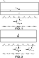
- Fig. 1 shows a sensor according to the prior art.
- the source and the drain are not depicted but they would be present respectively on the left and the right of the channel (2).
- the sensor (1) can be represented by a chain of transistors or as a chain of resistors in a circuit schematic.
- a molecular probe (5) is shown on a dielectric region (3).
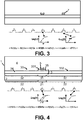
- Fig. 2 Docked charged target molecules (6) cause a local threshold shift which changes the resistance. Because the local resistance underneath a docked molecule is small compared to the resistance of the entire channel, a change in this local resistance induced by the docked molecule will result in a small overall resistance modulation.
- a fouling molecule (7) which does not dock onto the target binding site (which only dock the target molecule) but attaches non-specifically to the gate dielectric causes a similar modulation of resistance and hence results in a false positive signal.
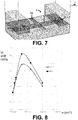
- the sensor comprises a field effect transistor which comprises an active region.
- the active region comprises a source region and a drain region (not shown) defining a source-drain axis.
- the active region further comprises a channel region (2) between the source region and the drain region.
- the field effect transistor further comprises a dielectric region (3) composed of a common dielectric layer (34) (e.g. SiO 2 ) covering the first (31) and the second (32) portion of the channel and comprises a further dielectric strip (35) (e.g. HfO 2 ).
- This dielectric region (3) is on the channel region.
- This dielectric region (3) comprises at least a first zone (31) on a first portion (21) of the channel region and a second zone (32) on a second portion (22) of the channel region.
- the first zone measures from 1 to 100 nm in the direction of the source-drain axis.
- the first zone has a top surface (331) while the second zone has a top surface (332). Both top surfaces differ in their chemical nature, thereby participating to the formation of a lower threshold voltage (more negative) for the first portion of the channel region than for the second portion of the channel region.
- the field effect transistor further comprises a fluidic gate region (4) to which a top surface (33) of the dielectric region is exposed.
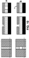
- FIG. 7 shows a Technology Computer Aided Design (TCAD) simulation setup of a sensor according to an embodiment of the present invention. It simulated an active region having a 10 nm x 5 nm cross-section and comprising a source (8), a drain (9) and a 2e17 cm -3 n-type doped channel (2) therebetween.
- the dielectric region comprising a first and a second zone was simulated by a 1 nm thick common SiO 2 dielectric layer covering the whole channel and corresponding to the second zone (not visible) and a Si 3 N 4 strip (35) on the common dielectric layer to form the first zone.
- the dielectric strip has a width equal to the width of the channel.
- a fluidic gate region (4) was simulated as containing water and 0.154 mol/l NaCl as the electrolyte.
- Another simulation setup was performed, identical to the one of Fig. 7 , except for the absence of the strip of further dielectric material. In absence of the dielectric strip, the modulation created by one electron charge placed 1 nm above the common dielectric layer, when a 15 mV s/d bias is applied, was 1mV. Both simulations were repeated for an active region having a 10 nm x 10 nm cross-section.
- Vt shift, mV/q The dependence of the modulation of threshold voltage (Vt shift, mV/q) is shown as a function of the charge density (cm -2 ) at the surface of the dielectric strip in figure 8 .
- the calculations showed that the threshold modulation increases from 1mV to about 3 mV (10 nm x 10 nm) or 3.5mV (10 nm x 5 nm) by introducing the dielectric strip. The threshold modulation was therefore better when the channel was thinner. It was further observed that the enhancement obtained depended on the extent of the strip along the source-drain axis, channel dimensions and charges of the dielectric.
- the thickness of the channel (measured perpendicularly to the top surface of the channel surface) was shown to play a role given that current seek to bypass the mobile charge decrease induced by the dielectric and the molecular charge by running deeper in the channel. This can be countered by thinning the channel by e.g. working with Ultra thin SOI or quantum wells such as SiGe/Si. Concerning the dimensions of the first zone, the shorter the first zone along the source-drain axis, the more efficiently a molecule will be able to modulate a sufficiently large part of the slit or strip. However, below a certain length, gating becomes inefficient.
- the size of the slit or strip can be defined to be below ⁇ 100nm and down to a few nanometers by making use of e.g. self-aligned double patterning (SADP).
- SADP self-aligned double patterning
- Fig. 9 to 14 where it is shown that an area for selective functionalization can be defined both longitudinally and transversally.
- an active region (10) embedded in an isolation material (11) which features a non-SiO 2 dielectric on the surface (Al 2 O 3 or HfO 2 for instance, but not limited to these, figure 9a ).
- an ALD or CVD dielectric coating (12) is deposited (for instance HfO 2 or Al 2 O 3 , materials are not limited to these, figure 9b ).
- SADP for instance a (hard)mask (13) is formed with a nanometer sized slit (14) ( figure 10a ).
- the underlying dielectric coating (12) is etched (wet and/or dry), in this particular case down to the Si channel of the active layer 10) ( figure 10b ), one may also stop on SiO 2 .
- the mask (13) is then stripped ( figure 11a ).
- the SiO 2 (31) is regrown on the longitudinally and transversally defined nano-sized area on the channel (2) ( figure 11b ). Hence one obtains a nano-sized surface (31) of SiO 2 which can additionally be differentially functionalized with molecules vs. the surrounding material (32).
Landscapes
- Health & Medical Sciences (AREA)
- Life Sciences & Earth Sciences (AREA)
- Chemical & Material Sciences (AREA)
- Molecular Biology (AREA)
- Physics & Mathematics (AREA)
- Engineering & Computer Science (AREA)
- General Health & Medical Sciences (AREA)
- Spectroscopy & Molecular Physics (AREA)
- Chemical Kinetics & Catalysis (AREA)
- Electrochemistry (AREA)
- Analytical Chemistry (AREA)
- Biochemistry (AREA)
- Microelectronics & Electronic Packaging (AREA)
- General Physics & Mathematics (AREA)
- Immunology (AREA)
- Pathology (AREA)
- Nanotechnology (AREA)
- Crystallography & Structural Chemistry (AREA)
- Investigating Or Analyzing Materials By The Use Of Electric Means (AREA)
Abstract
Description
- The present invention relates to the field of Field-effect transistor-based biosensors (bioFETs) and to method of making and using the same.
- BioFETs sense molecules as charge or dielectric displacements close to their gate dielectric. These transistors do not have their solid gate electrode directly in contact with the gate dielectric. Instead, they have a liquid electrolyte gate in contact with the gate dielectric and the solid gate electrode is in electrical contact with the liquid electrolyte gate. The sensed molecules are located in this liquid gate at or near the gate dielectric surface. The molecular charge or dielectric displacement near the gate dielectric causes a change in the current running through the semiconductor channel of the device as dictated by the disturbance in the electrical potential landscape these molecules cause. Such devices are currently considered promising for single molecule detection and highly sensitive molecular detection.
- One of the main contemporary obstacles inhibiting the effectivity of such single molecule and highly sensitive FET devices is the weak signal a single electronic charge / molecule generates for FET devices of a size currently deemed manufacturable in top-down semiconductor manufacturing technologies. One key cause of the weak signal is the screening of molecular charges by the electrolyte. For biologically relevant sensing applications the salt concentration has to be near physiological levels which introduces significant screening. The physiological NaCI concentration is 154mM at which the Debye length becomes smaller than 1nm. Depending on the application, salinity can be lowered but screening remains a central issue. A second key issue is bio-fouling which originates from non-target molecules which bind to the FET sensor and cause false signals.
- Hence, there is a need in the art for BioFETs overcoming at least partly one or more of the above issues.
- It is an object of the present invention to provide good apparatus or methods for sensing molecules in a liquid medium.
- It is an advantage of sensors according to embodiments of the present invention that they have a good sensitivity. For instance, in some embodiments, single molecules can be detected.
- It is an advantage of sensors according to embodiments of the present invention that they have high selectivity or specificity. Indeed, they are not very impacted by fouling.
- It is an advantage of sensors according to embodiments of the present invention that they are relatively inexpensive to produce. An alternative way to increase sensitivity would be to shorten the channel length by shortening the distance between the source region and the drain region but the smaller this distance, the more difficult it becomes to form steep doping profiles for the source and drain, hence raising the costs. Embodiments of the present invention permit to obtain the sensitivity of a shorter such distance without having to actually shorten that distance.
- The above objective is accomplished by a method and device according to the present invention.
- In a first aspect, the present invention relates to a sensor. The sensor comprises a field effect transistor. The field effect transistor comprises an active region. The active region comprises a source region and a drain region defining a source-drain axis. The active region further comprises a channel region between the source region and the drain region. The field effect transistor further comprises a dielectric region. This dielectric region is on the channel region. This dielectric region comprises at least a first zone on a first portion of the channel region and a second zone on a second portion of the channel region. The first zone measures from 1 to 100 nm in the direction of the source-drain axis. The first zone is adapted to create a different threshold voltage for the first portion of the channel region than for the second portion of the channel region. The field effect transistor further comprises a fluidic gate region to which a top surface of the dielectric region is exposed.
- In embodiments, the first zone may be adapted to create a different threshold voltage for the first portion by having a different dielectric charge density at the interface between the first zone and the first portion.
- In a second aspect, the present invention relates to a biosensing device comprising a sensor according to any embodiment of the first aspect.
- In a third aspect, the present invention relates to a process for forming a sensor according to any embodiment of the first aspect, comprising the steps of:
- a. Providing an active region (typically on a substrate), the active region having a source region, a drain region and a channel region therebetween,
- b. Providing a dielectric region on the channel region, the dielectric region comprising at least a first zone on a first portion of the channel region and a second zone on a second portion of the channel region, the first zone measuring from 1 to 100 nm and preferably at most 50 nm in the direction of the source-drain axis and being adapted to create a different threshold voltage for the first portion of the channel region than for the second portion of the channel region, and
- c. Providing a fluidic gate region to which a top surface of the dielectric region is exposed.
- In a fourth aspect, the present invention relates to a method for detecting the possible presence of an analyte in a liquid medium.
- In an embodiment, the method may comprise the steps of:
- a. Providing a sensor according to any embodiment of the first aspect,
- b. Applying a gate potential and measuring a first current between the source region and the drain region,
- c. Introducing the liquid medium potentially containing the analyte in the fluidic gate region, and
- d. Measuring a second current between the source region and the drain region, thereby detecting the analyte.
- After step c, the first zone is in contact with the liquid medium.
- Particular and preferred aspects of the invention are set out in the accompanying independent and dependent claims. Features from the dependent claims may be combined with features of the independent claims and with features of other dependent claims as appropriate and not merely as explicitly set out in the claims.
- Although there has been constant improvement, change and evolution of devices in this field, the present concepts are believed to represent substantial new and novel improvements, including departures from prior practices, resulting in the provision of more efficient, stable and reliable devices of this nature.
- The above and other characteristics, features and advantages of the present invention will become apparent from the following detailed description, taken in conjunction with the accompanying drawings, which illustrate, by way of example, the principles of the invention. This description is given for the sake of example only, without limiting the scope of the invention. The reference figures quoted below refer to the attached drawings.
-
-
Fig. 1 shows a vertical cross-section of a sensor according to the prior art in absence of analyte; below the cross-section is a schematic representation of the sensor channel as a series of virtual transistors; below the transistor corresponding to a section of the channel on which a molecular probe is present, is its corresponding graph of Log(I) as a function of V; below that graph is a schematic representation of the sensor channel as series of resistors. -
Fig. 2 shows the vertical cross-section ofFig.1 in presence of an analyte and the changes to the graph of Log(I) as a function of V resulting from this presence. -
Fig. 3 shows the vertical cross-section ofFig.1 in presence of a fouling molecule and the changes to the graph of Log(I) as a function of V resulting from this presence. -
Fig. 4 shows a vertical cross-section of a sensor according to an embodiment of the present invention in absence of analyte; below the cross-section is a schematic representation of the sensor channel as a series of virtual transistors; below the transistor corresponding to a section of the first portion of the channel on which a molecular probe is present, is its corresponding graph of Log(I) as a function of V; below the transistor corresponding to a section of the second portion of the channel on which a molecular probe is not present, is its corresponding graph of Log(I) as a function of V; below these graphs are a schematic representation of the sensor channel as series of resistors. -
Fig. 5 shows the vertical cross-section ofFig.4 in presence of an analyte and the changes to the graphs of Log(I) as a function of V resulting from this presence. -
Fig. 6 shows the vertical cross-section ofFig.4 in presence of a fouling molecule and the changes to the graphs of Log(I) as a function of V resulting from this presence. -
Fig. 7 is a Technology Computer Aided Design (TCAD) simulation setup of a sensor according to an embodiment of the present invention. -
Fig. 8 is a Graph showing the shift in threshold voltage as a function of the negative volume charge density for simulations as shown inFig. 7 . -
Figs. 9 to 11 show cross-sections and top views of intermediates obtained after various steps in the formation of a sensor according to an embodiment of the present invention. The top view is on the right. On the left is a vertical cross-section taken along the vertical dashed line shown in the top view. In the middle is a vertical cross-section taken along the horizontal dashed line shown in the top view. -
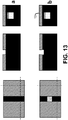
Figs. 12 to 14 show cross-sections and top views of intermediates obtained after various steps in the formation of a sensor according to another embodiment of the present invention. The top view is on the right. On the left is a vertical cross-section taken along the vertical dashed line shown in the top view. In the middle is a vertical cross-section taken along the horizontal dashed line shown in the top view. - In the different figures, the same reference signs refer to the same or analogous elements.
- The present invention will be described with respect to particular embodiments and with reference to certain drawings but the invention is not limited thereto but only by the claims. The drawings described are only schematic and are non-limiting. In the drawings, the size of some of the elements may be exaggerated and not drawn on scale for illustrative purposes. The dimensions and the relative dimensions do not correspond to actual reductions to practice of the invention.
- Furthermore, the terms first, second, third and the like in the description and in the claims, are used for distinguishing between similar elements and not necessarily for describing a sequence, either temporally, spatially, in ranking or in any other manner. It is to be understood that the terms so used are interchangeable under appropriate circumstances and that the embodiments of the invention described herein are capable of operation in other sequences than described or illustrated herein.
- Moreover, the terms top, bottom, over, under and the like in the description and the claims are used for descriptive purposes and not necessarily for describing relative positions. It is to be understood that the terms so used are interchangeable under appropriate circumstances and that the embodiments of the invention described herein are capable of operation in other orientations than described or illustrated herein.
- It is to be noticed that the term "comprising", used in the claims, should not be interpreted as being restricted to the means listed thereafter; it does not exclude other elements or steps. It is thus to be interpreted as specifying the presence of the stated features, integers, steps or components as referred to, but does not preclude the presence or addition of one or more other features, integers, steps or components, or groups thereof. The term "comprising" therefore covers the situation where only the stated features are present and the situation where these features and one or more other features are present. Thus, the scope of the expression "a device comprising means A and B" should not be interpreted as being limited to devices consisting only of components A and B. It means that with respect to the present invention, the only relevant components of the device are A and B.
- Reference throughout this specification to "one embodiment" or "an embodiment" means that a particular feature, structure or characteristic described in connection with the embodiment is included in at least one embodiment of the present invention. Thus, appearances of the phrases "in one embodiment" or "in an embodiment" in various places throughout this specification are not necessarily all referring to the same embodiment, but may. Furthermore, the particular features, structures or characteristics may be combined in any suitable manner, as would be apparent to one of ordinary skill in the art from this disclosure, in one or more embodiments.
- Similarly it should be appreciated that in the description of exemplary embodiments of the invention, various features of the invention are sometimes grouped together in a single embodiment, figure, or description thereof for the purpose of streamlining the disclosure and aiding in the understanding of one or more of the various inventive aspects. This method of disclosure, however, is not to be interpreted as reflecting an intention that the claimed invention requires more features than are expressly recited in each claim. Rather, as the following claims reflect, inventive aspects lie in less than all features of a single foregoing disclosed embodiment. Thus, the claims following the detailed description are hereby expressly incorporated into this detailed description, with each claim standing on its own as a separate embodiment of this invention.
- Furthermore, while some embodiments described herein include some but not other features included in other embodiments, combinations of features of different embodiments are meant to be within the scope of the invention, and form different embodiments, as would be understood by those in the art. For example, in the following claims, any of the claimed embodiments can be used in any combination.
- Furthermore, some of the embodiments are described herein as a method or combination of elements of a method that can be implemented by a processor of a computer system or by other means of carrying out the function. Thus, a processor with the necessary instructions for carrying out such a method or element of a method forms a means for carrying out the method or element of a method. Furthermore, an element described herein of an apparatus embodiment is an example of a means for carrying out the function performed by the element for the purpose of carrying out the invention.
- In the description provided herein, numerous specific details are set forth. However, it is understood that embodiments of the invention may be practiced without these specific details. In other instances, well-known methods, structures and techniques have not been shown in detail in order not to obscure an understanding of this description.
- The invention will now be described by a detailed description of several embodiments of the invention. It is clear that other embodiments of the invention can be configured according to the knowledge of persons skilled in the art without departing from the technical teaching of the invention, the invention being limited only by the terms of the appended claims.
- In a first aspect, the present invention relates to a sensor comprising a field effect transistor (FET) comprising:
- an active region comprising:
- ∘ a source region and a drain region defining a source-drain axis,
- ∘ a channel region between the source region and the drain region,
- a dielectric region on the channel region, comprising at least a first zone on a first portion of the channel region and a second zone on a second portion of the channel region, the first zone measuring from 1 to 100 nm in the direction of the source-drain axis and being adapted to create a different threshold voltage for the first portion of the channel region than for the second portion of the channel region, and
- a fluidic gate region to which a top surface of the dielectric region is exposed.
- The sensor may typically be for sensing a molecule (typically a charged molecule) in a liquid medium. Most typically, the molecule may be a biomolecule. Most typically, the liquid medium may be an aqueous electrolyte medium such as a biological fluid.
- The sensor typically further comprises a solid gate electrode for applying a potential difference between the liquid electrolyte gate and the channel. In embodiments, the solid gate electrode may be placed so that it can come in physical and electrical contact with the liquid medium.
- The active region comprises one or more semiconductor materials. In embodiments, the active region may comprise one or more group IV (e.g. Si, Ge, SixGey, or heterostructures of layers thereof) or III-V materials (e.g. GaAs). In embodiments, the active region may be made of Si. The source and the drain regions are defined in the active region as two regions spatially separated from each other and being less resistive than the region separating them. They can for instance be formed by doping. The region separating the source and the drain is the channel.
- In embodiments, the active region may have a thickness (measured perpendicularly to a top surface of the active region) of at most 100 nm, preferably at most 50 nm (for instance from 2 to 10 nm or from 2 to 5 nm). A thinner active region can prevent current from bypassing the region of altered (typically increased) resistance caused by the first zone of the dielectric region by running underneath it. The active region can take various forms such as the form of a layer or the form of a nanowire. It can for instance be made of Si (e.g. from Si bulk or from a SOI). To obtain an active region of a low thickness, the top semiconductor layer of an SOI (such as an Ultra thin SOI) can for instance be used. An alternative to obtain an active region of a low thickness is to form the active region in a bulk Si substrate in which the part close to the channel has doping different from the rest of the Si bulk substrate (for instance higher than the rest or lower than the rest).
- The dielectric region on the channel region can be referred to as the gate dielectric. It can be made of a single material or of a combination of materials. It comprises at least a first zone and a second zone. In embodiments, it may comprise (or consist of) a first zone and a second zone wherein the second zone either surround the first zone or is split in two by the first zone. The first zone can be centred with respect to the channel but it can also be located closer to the source than to the drain or closer to the drain than to the source. It is preferred if the first zone is closer to the drain than to the source because the drain is typically at a higher voltage, leading to effectively smaller channel-gate potential difference near the drain. The first zone is however typically not adjacent to the source or to the drain, i.e. it is typically separated from both the source and the drain by the second zone.
- In embodiments, where the second zone surrounds the first zone, the first zone may have any shape such as a square shape, a round shape or an irregular shape.
- In embodiments, a nanocavity or nanopore may cross the channel perpendicularly to the source-drain axis and may open in the first zone. The present invention is however particularly useful when the channel is not crossed by a nanocavity or a nanopore.
- In embodiments, the first zone may measure (i.e. have a length of) from 1 to 100 nm in the direction of the source-drain axis. The length of the first zone along the source-drain axis is preferably from 1 to 50 nm. In embodiments, the length of the first zone may be from 5 to 50%, preferably from 10 to 35%, more preferably from 15 to 25% of the channel length. Small dimensions for the first zone can be achieved for instance by using self-aligned multiple (e.g. double) patterning.
- In embodiments, the width of the first zone (measured in the plane of the top surface of the first zone and perpendicularly to the source drain axis) may be at least 50%, preferably at least 75%, more preferably at least 90% of the width of the channel. Most preferably, the first zone occupies the whole width of the channel (and thereby splits the second zone in two).
- In embodiments, the width of the channel may be from 3 to 60 nm.
- In embodiments, where the second zone is split in two by the first zone, the first zone may have the shape of a strip (e.g. it is thicker than the second zone) or of a slit (i.e. it is thinner than the second zone). The longitudinal extent of the slit or strip is typically perpendicular to the source drain axis.
- In any embodiments, the first zone may be demarcated from the second zone by a difference of material, a difference of height (i.e. a difference in thickness), a difference in doping, or a combination thereof.
- Examples where the first zone is demarcated from the second zone by a difference of material (i.e. the first zone and the second zone differ in their chemical composition) include but are not limited to the following configurations. The first zone may be made of a first bulk material and the second zone may be made of a second bulk material (e.g. two different dielectric materials, eventually differing in their k-value). The first zone may be composed of a different number of layers of different materials than the second zone. The first zone and the second zone may be composed of the same number of layers of the same material but in different orders so that the layer forming the top surface of the first zone is of a different material than the layer forming the top surface of the second zone. The first zone and the second zone may be made different by functionalizing their top surfaces differently. For instance, the first zone and the second zone may be made of a single layer of the same bulk dielectric material, but their top surfaces may be functionalized differently (e.g. providing a difference in charge density). This can for instance be achieved by forming a self-assembled monolayer on the first zone or on the second zone, or by forming a different self-assembled monolayer on the first zone and on the second zone. In embodiments, the first and second zone may both have a same self-assembled monolayer thereon, in which case the first and the second zone differ in other aspects. The self-assembled monolayer may be formed of molecules having a functional group for attaching to the top surface of the single dielectric layer, a functional group for providing surface properties, and a linker for linking both functional groups. The surface property sought after may for instance be an electrical property (e.g. via charged groups), an antifouling property (e.g. via bovine serum albumin), or may be a selectivity toward the analyte (e.g. via a molecular probe). The functional group for providing surface properties may for instance be charged in presence of the liquid medium in which the analyte is present. Examples of functional groups for providing the surface properties may be neutral hydrophilic groups (e.g. polyethylene glycol), charged hydrophilic groups (e.g. COOH or NH3 which are susceptible to be charged in an aqueous medium depending on the pH), hydrophobic groups (e.g. alkanes), or biomolecules (e.g. the protein bovine serum albumin). The functional group for attaching to the top surface may for instance be silane groups (e.g. for functionalizing SiO2), phosphonic acid groups (e.g. for functionalizing Al2O3 or HfO2).
- Preferably the top surface of the second zone may belong to a SiO2 layer while the top surface of the first zone may belong to a layer of another dielectric material.
- For instance, the second zone may be made of a layer or SiO2 while the first zone may be made of a layer of SiO2 with another dielectric material on top thereof. Examples of dielectric materials for the other dielectric material are high-k dielectric materials. Examples of high-k materials comprise but are not limited to Al2O3, HfO2, SiON, Si3N4, and Ta2O5.
- Examples where the first zone is demarcated from the second zone by a difference of height (i.e the first zone and the second zone differ in thickness) include but are not limited to the following configurations. The first zone may be thicker/higher than the second zone. The first zone may be thinner/lower than the second zone.
- For instance, the first zone may comprise a strip of a further material on a first dielectric material common to both the first and the second zone. As another example, the first zone may be delimited by a slit in a further material on a first dielectric material.
- The local channel resistance is different underneath the slit or strip (i.e. in the first portion of the channel) than in the second portion of the channel.
- In any embodiments, the further layer/material may be a dielectric layer.
- Preferably, the local channel resistance is larger underneath the slit or strip (i.e. in the first portion of the channel) than in the second portion of the channel.
- In any embodiments, the further layer/material may be a dielectric layer.
- The first zone may also be demarcated from the second zone by a difference in doping. In some of these embodiments, the field effect transistor may be of an n-type and the first zone may be negatively doped while the second zone is less negatively doped or is positively doped; or the field effect transistor may be of a p-type and the first zone may be positively doped while the second zone is less positively doped or is negatively doped. Most preferably, when the first zone and/or the second zone is doped, the corresponding first and second portions of the channel are not doped or present a lower dopant concentration than the corresponding first and/or second zone.
- In embodiments, a top surface of the first zone may be charged differently than a top surface of the second zone. In some of these embodiments, the field effect transistor may be of an n-type and the top surface of the first zone may be negatively charged while the top surface of the second zone is less negatively charged or is positively charged, or the field effect transistor may be of a p-type and the top surface of the first zone may be positively charged while the top surface of the second zone is less positively charged or is negatively charged. When the first zone is said to be charged, it is meant that it is such that it can be charged when in contact with an aqueous medium (e.g. with a biological fluid).
- When the first zone is said to be adapted to create a different threshold voltage for the first portion of the channel region than for the second portion of the channel region, it is not necessary to quantify this difference. It is enough if the first zone has been adapted so that there is a difference. Ways to achieve a difference in threshold voltage for the first portion may for instance be achieved by having the first zone differing from the second zone in the following way: a difference in thickness, a difference in material (for instance providing a difference in k-value), a difference in doping, or a combination thereof.
- Although quantification of the difference is not necessary for the invention to work, in embodiments, the first zone may be adapted to create a difference in threshold voltage of at least 1 mV, preferably at least 2 mV, yet more preferably at least 3 mV in the first portion of the channel region with respect to the second portion. Larger differences provide larger sensitivity and selectivity.
- The threshold voltage can be evaluated by using usual simulation softwares well known to the person skilled in the art. The threshold voltage can be approached by the following formula:

- VT is the threshold voltage in the portion of interest (e.g. first portion) of the channel region,
- VFB is the flatband voltage given by the formula

- φn is the potential of the portion of interest of the channel region,
- φµ is the potential of the gate electrode,
- QI is the dielectric charge density at the interface between the zone of interest of the dielectric region (e.g. first zone) and the portion of interest of the channel region (e.g. first portion),
- tox is the thickness of the zone of interest of the dielectric region,
- εox is the dielectric constant of the zone of interest of the dielectric region,
- εSi is the dielectric constant of the portion of interest of the channel region, q is the electronic charge,
- ND is the doping of the portion of interest of the channel region,
- The amount of charge inside the dielectric impacts the threshold voltage through the flatband voltage which has the term QI. Any charge inside the dielectric can be translated into an equivalent QI.
- In embodiments, the field effect transistor may either be of an n-type and the first zone is adapted to create a higher (more positive) threshold voltage for the first portion of the channel region than for the second portion of the channel region, or the field effect transistor may be of a p-type and the first zone is adapted to create a lower threshold voltage (more negative) for the first portion of the channel region than for the second portion of the channel region. In other words, the field effect transistor may either be of an n-type or of a p-type and the first zone may be adapted to create a higher resistance in the first portion of the channel region than in the second portion of the channel region.
- In embodiments of the first aspect, the present invention relates to a sensor comprising a field effect transistor (FET) comprising:
- an active region comprising:
- ∘ a source region and a drain region defining a source-drain axis,
- ∘ a channel region between the source region and the drain region,
- a dielectric region on the channel region, comprising at least a first zone on a first portion of the channel region and a second zone on a second portion of the channel region, the first zone measuring from 1 to 100 nm in the direction of the source-drain axis and wherein the following applies:
- ∘ a top surface of the first zone is charged differently than a top surface of the second zone, and/or
- ∘ the first zone differs from the second zone by the materials it comprises, and/or
- ∘ the first zone differs from the second zone by its thickness, and/or
- ∘ the first zone differs from the second zone by its doping, and
- a fluidic gate region to which a top surface of the dielectric region is exposed.
- In some of the embodiments where the field effect transistor is either of an n-type and the first zone is adapted to create a higher threshold voltage for the first portion of the channel region than for the second portion of the channel region, or the field effect transistor is of a p-type and the first zone is adapted to create a lower threshold voltage for the first portion of the channel region than for the second portion of the channel region, the top surface of the first zone may have a point of zero charge differing by at least 1 with respect to the point of zero charge of the top surface of the second zone. In some of these embodiments, the field effect transistor may be of an n-type and the top surface of the first zone may have a point of zero charge lower than the point of zero charge of the top surface of the second zone or the field effect transistor may be of a p-type and the top surface of the first zone may have a point of zero charge higher than the point of zero charge of the top surface of the second zone.
- For instance, in some of these embodiments, the field effect transistor may be of an n-type and the top surface of the first zone may be SiO2 having a point of zero charge of about 2 while the top surface of the second zone may be HfO2 having a point of zero charge of about 7.
- As another example, the field effect transistor may be of an p-type and the top surface of the first zone may be HfO2 having a point of zero charge of about 7 while the top surface of the second zone may be SiO2 having a point of zero charge of about 2.
- In embodiments, the first zone and the second zone may comprise a common dielectric layer wherein the first zone or the second zone comprises a further layer (made of the same or of a different dielectric material) creating the different threshold. In embodiments, the common dielectric layer may be on the channel region (e.g. only) and the further layer may be on the common dielectric layer. For instance, the further layer may form a slit or a strip on the common dielectric layer. In these embodiments, if it is the first zone that comprises a further layer, the first zone will have a larger thickness than the second zone and if it is the second zone that comprises a further layer, the second zone will have a larger thickness that the first zone. In other embodiments, the further dielectric layer (made of the same material or of another material) may form part of the first or of the second zone and may be on the channel region while the common dielectric layer may be on the channel region and on the further dielectric layer. In these embodiments, if it is the first zone that comprises a further layer, the first zone will typically have a larger thickness than the second zone and if it is the second zone that comprises a further layer, the second zone will typically have a larger thickness that the first zone. It is however possible to form the common dielectric layer made of a first material on top of the further layer made of a second material, different from the first material, in such a way that the top surface of the dielectric region is planar. This can be achieved for instance by overfilling a split in the further dielectric layer with a liquid precursor to the common dielectric layer before to form the common dielectric layer from said precursor.
- When the different threshold voltage is higher in absolute value, this means that the local resistance in the first portion of the channel region will be larger than in the second portion of the channel region. This in turn means that the contribution of the first portion of the channel to the total resistance of the channel will be large relatively to the area it occupies. This in turn means that if a gate potential approaching (e.g. subthreshold operation) or surpassing in absolute value (and of same sign than) the threshold voltage of the first zone is applied between the source and the drain, the presence of a target molecule on the first zone will induce a larger change in the total resistance than the presence of that same target molecule on the second zone. It is also possible to use such a device by applying a gate potential intermediate between the threshold voltage of the first zone and the threshold voltage of the second zone (subthreshold operation). In these embodiments, it is preferred if this gate voltage is below (in absolute value) the threshold voltage of the first zone by an amount smaller than the decrease (in absolute value) in threshold voltage caused by the target molecule when it is present on the first zone. That way, significantly more current passes if a target molecule is present on the first zone than otherwise.
- The fluidic gate region is located above the dielectric region and it is suitable for exposing the dielectric region to the liquid medium. In some embodiments, the fluidic gate region is filled with the liquid medium. The liquid medium is typically an electrolyte containing the analyte and serving as a liquid gate. In some embodiments, the fluidic gate region is at least partially empty or not filled with a liquid. In some embodiments at least some of the fluidic gate region is filled with air. In some embodiments, an inlet is located on one side of the fluidic gate region and an outlet is located on the opposing side of the fluidic gate region. In some embodiments, a cover is located above the fluidic gate region and the fluidic gate region is defined by the cover, the dielectric region and sidewalls (e.g. connecting the cover and the dielectric region).
- In embodiments, a molecular probe, for specifically binding a target molecule to be detected by the sensor, may be attached to the exposed surface of the first zone. Examples of molecular probe are enzymes, antibodies, ligands, receptors, peptides, and oligo- or poly-nucleotides.
- In a second aspect, the present invention relates to a biosensing device comprising a sensor according to any embodiment of the first aspect.
- In a third aspect, the present invention may relate to a process for forming a sensor according to any one of the preceding claims, comprising the steps of:
- a. Providing an active region (typically on a substrate), the active region having a source region, a drain region and a channel region therebetween,
- b. Providing a dielectric region on the channel region, the dielectric region comprising at least a first zone on a first portion of the channel region and a second zone on a second portion of the channel region, the first zone measuring from 1 to 100 nm and preferably from 1 to 50 nm in the direction of the source-drain axis and being adapted to create a different threshold voltage for the first portion of the channel region than for the second portion of the channel region, and
- c. Providing a fluidic gate region to which a top surface of the dielectric region is exposed.
- In embodiments, the process further comprises coupling a gate electrode to the source for applying a potential difference between the gate and the source. In embodiments, the gate electrode may be placed so that it can come in physical and electrical contact with the liquid medium.
- Any feature of the third aspect may be as correspondingly described for the first aspect.
- In a fourth aspect, the present invention relates to a method for detecting the possible presence of an analyte in a liquid medium.
- In an embodiment, the method may comprise the steps of:
- a. Providing a sensor according to any embodiment of the first aspect,
- b. Applying a gate potential and measuring a first current between the source region (8) and the drain region (9),
- c. Introducing the liquid medium potentially containing the analyte in the fluidic gate region, and
- d. Measuring a second current between the source region and the drain region, thereby detecting the analyte.
- After step c, the first zone is in contact with the liquid medium.
- Step b of applying a gate potential can form instance comprise applying a gate potential having a value larger than the threshold potential of the second portion.
- In an embodiment, the gate potential applied in step b may have a value intermediate between the threshold potential of the first portion and the threshold potential of the second portion of the channel region.
- In another embodiment, the gate potential applied in step b may have a value larger in absolute value and of same sign than the threshold potential of the first portion and the threshold potential of the second portion of the channel region.
- The analyte (also referred to herein as the target molecule) is typically a biomolecule (such as a protein or a polynucleotide single strand) or a biological entity (such as an organelle or a cell). Preferably, it is a charged molecule.
- One way to perform a measurement is to introduce a reset solution (electrolyte solution without the analyte) into the fluidic gate region; recording a reset value, introducing a sample containing an analyte into the fluidic gate region; recording a sensing value; and obtain a difference between the sensing value and the reset value.
- The measurement of the first current in step b can for instance be measured without a liquid in the fluidic region, with a liquid medium not containing the analyte (e.g. a reset solution), or with a liquid medium comprising a known concentration of the analyte (e.g. a reference solution).
- If step b is performed in presence of a liquid in the fluidic region, step c can comprise replacing that liquid by the liquid medium potentially containing the analyte.
- In step d, detecting the analyte typically comprises comparing the first and the second current. A difference between these currents indicates the presence of an analyte.
- We now refer to
Fig. 1 which shows a sensor according to the prior art. The source and the drain are not depicted but they would be present respectively on the left and the right of the channel (2). In a simplified picture, along the length of the channel, the sensor (1) can be represented by a chain of transistors or as a chain of resistors in a circuit schematic. A molecular probe (5) is shown on a dielectric region (3). A graph of the Log(I) as a function of V, where I is the current intensity and V is the gate potential, is depicted for the local area of the channel where the molecular probe is present. - We now refer to
Fig. 2 . Docked charged target molecules (6) cause a local threshold shift which changes the resistance. Because the local resistance underneath a docked molecule is small compared to the resistance of the entire channel, a change in this local resistance induced by the docked molecule will result in a small overall resistance modulation. - We now refer to
Fig. 3 . A fouling molecule (7) which does not dock onto the target binding site (which only dock the target molecule) but attaches non-specifically to the gate dielectric causes a similar modulation of resistance and hence results in a false positive signal. - We now refer to
Fig. 4 which shows an pMOS sensor (1) according to an embodiment of the present invention. The sensor comprises a field effect transistor which comprises an active region. The active region comprises a source region and a drain region (not shown) defining a source-drain axis. The active region further comprises a channel region (2) between the source region and the drain region. The field effect transistor further comprises a dielectric region (3) composed of a common dielectric layer (34) (e.g. SiO2) covering the first (31) and the second (32) portion of the channel and comprises a further dielectric strip (35) (e.g. HfO2). This dielectric region (3) is on the channel region. This dielectric region (3) comprises at least a first zone (31) on a first portion (21) of the channel region and a second zone (32) on a second portion (22) of the channel region. The first zone measures from 1 to 100 nm in the direction of the source-drain axis. The first zone has a top surface (331) while the second zone has a top surface (332). Both top surfaces differ in their chemical nature, thereby participating to the formation of a lower threshold voltage (more negative) for the first portion of the channel region than for the second portion of the channel region. - The field effect transistor further comprises a fluidic gate region (4) to which a top surface (33) of the dielectric region is exposed.
- We now refer to
Fig. 5 . As a consequence, when the target charged molecule docks onto a target binding site on the strip, the change in resistance measured by the sensor is larger because the resistance underneath the strip is high compared to the rest of the channel. - We now refer to
Fig. 6 . When a molecule binds non-specifically on the channel surface next to the strip the modulation caused by this molecule is smaller than that by the target molecule on the strip due to the relatively lower local resistance of the remainder of the channel. -
Figure 7 shows a Technology Computer Aided Design (TCAD) simulation setup of a sensor according to an embodiment of the present invention. It simulated an active region having a 10 nm x 5 nm cross-section and comprising a source (8), a drain (9) and a 2e17 cm-3 n-type doped channel (2) therebetween. The dielectric region comprising a first and a second zone was simulated by a 1 nm thick common SiO2 dielectric layer covering the whole channel and corresponding to the second zone (not visible) and a Si3N4 strip (35) on the common dielectric layer to form the first zone. The dielectric strip has a width equal to the width of the channel. A fluidic gate region (4) was simulated as containing water and 0.154 mol/l NaCl as the electrolyte. Another simulation setup was performed, identical to the one ofFig. 7 , except for the absence of the strip of further dielectric material. In absence of the dielectric strip, the modulation created by one electron charge placed 1 nm above the common dielectric layer, when a 15 mV s/d bias is applied, was 1mV. Both simulations were repeated for an active region having a 10 nm x 10 nm cross-section. - The dependence of the modulation of threshold voltage (Vt shift, mV/q) is shown as a function of the charge density (cm-2) at the surface of the dielectric strip in
figure 8 . The calculations showed that the threshold modulation increases from 1mV to about 3 mV (10 nm x 10 nm) or 3.5mV (10 nm x 5 nm) by introducing the dielectric strip. The threshold modulation was therefore better when the channel was thinner. It was further observed that the enhancement obtained depended on the extent of the strip along the source-drain axis, channel dimensions and charges of the dielectric. The thickness of the channel (measured perpendicularly to the top surface of the channel surface) was shown to play a role given that current seek to bypass the mobile charge decrease induced by the dielectric and the molecular charge by running deeper in the channel. This can be countered by thinning the channel by e.g. working with Ultra thin SOI or quantum wells such as SiGe/Si. Concerning the dimensions of the first zone, the shorter the first zone along the source-drain axis, the more efficiently a molecule will be able to modulate a sufficiently large part of the slit or strip. However, below a certain length, gating becomes inefficient. The size of the slit or strip can be defined to be below < 100nm and down to a few nanometers by making use of e.g. self-aligned double patterning (SADP). - We now refer to
Fig. 9 to 14 where it is shown that an area for selective functionalization can be defined both longitudinally and transversally. In a first approach, one starts from an active region (10) embedded in an isolation material (11) which features a non-SiO2 dielectric on the surface (Al2O3 or HfO2 for instance, but not limited to these,figure 9a ). Then an ALD or CVD dielectric coating (12) is deposited (for instance HfO2 or Al2O3, materials are not limited to these,figure 9b ). Using SADP for instance a (hard)mask (13) is formed with a nanometer sized slit (14) (figure 10a ). Then using this mask (13) the underlying dielectric coating (12) is etched (wet and/or dry), in this particular case down to the Si channel of the active layer 10) (figure 10b ), one may also stop on SiO2. The mask (13) is then stripped (figure 11a ). Finally, and optionally, the SiO2 (31) is regrown on the longitudinally and transversally defined nano-sized area on the channel (2) (figure 11b ). Hence one obtains a nano-sized surface (31) of SiO2 which can additionally be differentially functionalized with molecules vs. the surrounding material (32). - One may also obtain a longitudinally and transversally defined non-native oxide area to be functionalized selectively. This can be obtained by starting off with an active region (10) embedded in an insulating matrix (with on top
dielectric material 12A) in which the channel is covered by a different ALD or CVD coating of dielectric (material 12B) (figure 12a ). Next, onedeposits material 12A (figure 12b ).Material 12A is then nano-patterned by using SADP for instance (figure 13a, 13b , and14 ). This opens a patch ofmaterial material - It is to be understood that although preferred embodiments, specific constructions and configurations, as well as materials, have been discussed herein for devices according to the present invention, various changes or modifications in form and detail may be made without departing from the scope of this invention. For example, any formulas given above are merely representative of procedures that may be used. Functionality may be added or deleted from the block diagrams and operations may be interchanged among functional blocks. Steps may be added or deleted to methods described within the scope of the present invention.
Claims (15)
- A sensor (1) comprising a field effect transistor comprising:• an active region (10) comprising:∘ a source region (8) and a drain region (9) defining a source-drain axis,∘ a channel region (2) between the source region and the drain region,• a dielectric region (3) on the channel region (2), comprising at least a first zone (31) on a first portion (21) of the channel region (2) and a second zone (32) on a second portion (22) of the channel region (2), the first zone (31) measuring from 1 to 100 nm in the direction of the source-drain axis and being adapted to create a different threshold voltage for the first portion (21) of the channel region (2) than for the second portion (21) of the channel region (2), and• a fluidic gate region (4) to which a top surface (33) of the dielectric region (3) is exposed.
- The sensor (1) according to claim 1, wherein the first zone (31) is adapted to create a difference in threshold voltage of at least 1 mV in the first portion (21) of the channel region (2) with respect to the second portion (22).
- The sensor (1) according to claim 1 or claim 2, wherein the field effect transistor is either of an n-type and the first zone (31) is adapted to create a higher threshold voltage for the first portion (21) of the channel region (2) than for the second portion (22) of the channel region (2), or the field effect transistor is of a p-type and the first zone (31) is adapted to create a lower threshold voltage for the first portion (21) of the channel region (2) than for the second portion (22) of the channel region (2).
- The sensor (1) according to any one of the preceding claims, wherein a top surface (331) of the first zone (31) is charged differently than a top surface (332) of the second zone (32).
- The sensor (1) according to claim 4, wherein either the field effect transistor is of an n-type and the top surface (331) of the first zone (31) is negatively charged while the top surface (332) of the second zone (32) is less negatively charged or is positively charged, or the field effect transistor is of a p-type and the top surface (331) of the first zone (31) is positively charged while the top surface (332) of the second zone (32) is less positively charged or is negatively charged.
- The sensor (1) according to claim 4 or claim 5, wherein the top surface (331) of the first zone (31) has a point of zero charge differing by at least 1 with respect to the point of zero charge of the top surface (332) of the second zone (32).
- The sensor (1) according to claim 6, wherein either the field effect transistor is of an n-type and the top surface (331) of the first zone (31) has a point of zero charge lower than the point of zero charge of the top surface (332) of the second zone (32) or the field effect transistor is of a p-type and the top surface (331) of the first zone (31) has a point of zero charge higher than the point of zero charge of the top surface (332) of the second zone (32).
- The sensor (1) according to any one of the preceding claims, wherein the first zone (31) and the second zone (32) differ in thickness.
- The sensor (1) according to any one of the preceding claims, wherein the first zone (31) and the second zone (32) differ in their chemical composition.
- The sensor (1) according to any one of the preceding claims, wherein the first zone (31) and the second zone (32) comprise a common dielectric layer (34) on the active region (2) and wherein the first zone (31) or the second zone (32) comprise a further layer (35) creating the different threshold.
- The sensor (1) according to any one of the preceding claims, wherein a molecular probe (5), for specifically binding a target molecule (6) to be detected by the sensor (1), is attached to the surface (331) of the first zone (31).
- The sensor (1) according to any one of the preceding claims, wherein the width of the first zone (31) is at least 50% of the width of the channel.
- A biosensing device comprising a sensor (1) according to any one of the preceding claims.
- A method for detecting the possible presence of an analyte (6) in a liquid medium, the method comprising:a. Providing a sensor (1) according to any of claims 1 to 12,b. Applying a gate potential and measuring a first current between the source region (8) and the drain region (9),c. Introducing the liquid medium potentially containing the analyte (6) in the fluidic gate region (4), andd. Measuring a second current between the source region (8) and the drain region (9), thereby detecting the analyte (6).
- A process for forming a sensor according to claim 1, comprising the steps of:a. Providing an active region (typically on a substrate), the active region having a source region, a drain region and a channel region therebetween,b. Providing a dielectric region on the channel region, the dielectric region comprising at least a first zone on a first portion of the channel region and a second zone on a second portion of the channel region, the first zone measuring from 1 to 100 nm and preferably from 1 to 50 nm in the direction of the source-drain axis and being adapted to create a different threshold voltage for the first portion of the channel region than for the second portion of the channel region, andc. Providing a fluidic gate region to which a top surface of the dielectric region is exposed.
Priority Applications (2)
| Application Number | Priority Date | Filing Date | Title |
|---|---|---|---|
| EP18192768.2A EP3620783B1 (en) | 2018-09-05 | 2018-09-05 | Field-effect transistor-based biosensor, method of fabrication thereof and method for detecting an analyte using said biosensor |
| US16/556,689 US11391692B2 (en) | 2018-09-05 | 2019-08-30 | Field-effect transistor-based biosensor |
Applications Claiming Priority (1)
| Application Number | Priority Date | Filing Date | Title |
|---|---|---|---|
| EP18192768.2A EP3620783B1 (en) | 2018-09-05 | 2018-09-05 | Field-effect transistor-based biosensor, method of fabrication thereof and method for detecting an analyte using said biosensor |
Publications (2)
| Publication Number | Publication Date |
|---|---|
| EP3620783A1 true EP3620783A1 (en) | 2020-03-11 |
| EP3620783B1 EP3620783B1 (en) | 2024-12-25 |
Family
ID=63517782
Family Applications (1)
| Application Number | Title | Priority Date | Filing Date |
|---|---|---|---|
| EP18192768.2A Active EP3620783B1 (en) | 2018-09-05 | 2018-09-05 | Field-effect transistor-based biosensor, method of fabrication thereof and method for detecting an analyte using said biosensor |
Country Status (2)
| Country | Link |
|---|---|
| US (1) | US11391692B2 (en) |
| EP (1) | EP3620783B1 (en) |
Families Citing this family (2)
| Publication number | Priority date | Publication date | Assignee | Title |
|---|---|---|---|---|
| EP4075131B1 (en) * | 2021-04-16 | 2025-03-19 | Imec VZW | Nanopore transistor for biosensing |
| CN120129316B (en) * | 2025-03-10 | 2025-11-21 | 西安电子科技大学 | A biosensor based on a parallel tunnel junction vertical tunneling field-effect transistor and its fabrication method. |
Citations (3)
| Publication number | Priority date | Publication date | Assignee | Title |
|---|---|---|---|---|
| US20040222446A1 (en) * | 2003-05-09 | 2004-11-11 | Chien-Sheng Yang | Ion sensitive field effect transistor and fabrication |
| US20130158378A1 (en) * | 2011-09-22 | 2013-06-20 | The Ohio State University | Ionic barrier for floating gate in vivo biosensors |
| US20170114402A1 (en) * | 2015-10-26 | 2017-04-27 | International Business Machines Corporation | Dna sequencing detection field effect transistor |
Family Cites Families (7)
| Publication number | Priority date | Publication date | Assignee | Title |
|---|---|---|---|---|
| KR100679704B1 (en) | 2005-01-10 | 2007-02-06 | 한국과학기술원 | Manufacturing method of nanogap or nanofield effect transistor for molecular device and biosensor |
| EP2165353B1 (en) | 2007-06-29 | 2017-08-30 | Applied Biosystems, LLC | Systems and methods for electronic detection with nanofets |
| US20120143027A1 (en) | 2007-12-19 | 2012-06-07 | Kimberly-Clark Worldwide, Inc. | Field effect transistors for detection of nosocomial infection |
| WO2011082178A1 (en) | 2009-12-29 | 2011-07-07 | Nanosense Inc. | Fet - based nanotube sensor array |
| US20140054651A1 (en) | 2010-12-08 | 2014-02-27 | The Board Of Trustees Of The University Of Illinois | Reliable nanofet biosensor process with high-k dielectric |
| US9958443B2 (en) | 2011-10-31 | 2018-05-01 | Taiwan Semiconductor Manufacturing Company, Ltd. | Signal enhancement mechanism for dual-gate ion sensitive field effect transistor in on-chip disease diagnostic platform |
| US9395326B2 (en) | 2013-11-01 | 2016-07-19 | Taiwan Semiconductor Manufacturing Company Limited | FET sensing cell and method of improving sensitivity of the same |
-
2018
- 2018-09-05 EP EP18192768.2A patent/EP3620783B1/en active Active
-
2019
- 2019-08-30 US US16/556,689 patent/US11391692B2/en active Active
Patent Citations (3)
| Publication number | Priority date | Publication date | Assignee | Title |
|---|---|---|---|---|
| US20040222446A1 (en) * | 2003-05-09 | 2004-11-11 | Chien-Sheng Yang | Ion sensitive field effect transistor and fabrication |
| US20130158378A1 (en) * | 2011-09-22 | 2013-06-20 | The Ohio State University | Ionic barrier for floating gate in vivo biosensors |
| US20170114402A1 (en) * | 2015-10-26 | 2017-04-27 | International Business Machines Corporation | Dna sequencing detection field effect transistor |
Also Published As
| Publication number | Publication date |
|---|---|
| US11391692B2 (en) | 2022-07-19 |
| US20200072788A1 (en) | 2020-03-05 |
| EP3620783B1 (en) | 2024-12-25 |
Similar Documents
| Publication | Publication Date | Title |
|---|---|---|
| US8853667B2 (en) | Quantum dot gate FETs and circuits configured as biosensors and gene sequencers | |
| US8940548B2 (en) | Sensor for biomolecules | |
| US9188594B2 (en) | Nanoelectronic-enzyme linked immunosorbent assay system and method | |
| US9076665B2 (en) | CMOS-compatible silicon nano-wire sensors with biochemical and cellular interfaces | |
| US9110014B2 (en) | Field effect transistor-based bio-sensor | |
| Rollo et al. | High performance Fin-FET electrochemical sensor with high-k dielectric materials | |
| US20140191186A1 (en) | Regenerative Nanosensor Devices | |
| Stoop et al. | Competing surface reactions limiting the performance of ion-sensitive field-effect transistors | |
| US20230022648A1 (en) | Biosensor having a fluid compartment | |
| US11391692B2 (en) | Field-effect transistor-based biosensor | |
| Singh et al. | Comparative analysis of gate structure dependent FET-based biosensor | |
| Mohanty et al. | Impact of biomolecules position and filling area on the sensitivity of hetero stack gate MOSFET | |
| US9417208B2 (en) | Dual FET sensor for sensing biomolecules and charged ions in an electrolyte | |
| EP3502688A1 (en) | Nanopore fet sensor with non-linear potential profile | |
| Kim et al. | A dual-gate field-effect transistor for label-free electrical detection of avian influenza | |
| US12345676B2 (en) | Field-effect transistor-based biosensor | |
| Fathil et al. | The ZnO-FET biosensor for cardiac troponin I | |
| EP4390393A1 (en) | Nanopore sensing device comprising multiple sensing layers | |
| US20200246793A1 (en) | Nanowire fet biomolecule sensors with integrated electroosmotic flow | |
| Mohanty et al. | Impact of bio-target location and their fill-in factor on the sensitivity of hetero channel double gate MOSFET label-free biosensor | |
| Huang et al. | Highly sensitive juntionless nanowire transistor biosensor in detecting breast tumor marker | |
| Tomoya et al. | Fabrication of N-Type Silicon Nanowire Biosensor for Sub-10-Femtomolar Concentration of Immunoglobulin | |
| Choi et al. | Dielectric detection using biochemical assays | |
| US20070166837A1 (en) | Nanoscale biomolecule sensor and method for operating same | |
| Gong et al. | Silicon Nanowire fabricated by MEMS technology and its application in biochemical detection |
Legal Events
| Date | Code | Title | Description |
|---|---|---|---|
| PUAI | Public reference made under article 153(3) epc to a published international application that has entered the european phase |
Free format text: ORIGINAL CODE: 0009012 |
|
| STAA | Information on the status of an ep patent application or granted ep patent |
Free format text: STATUS: THE APPLICATION HAS BEEN PUBLISHED |
|
| AK | Designated contracting states |
Kind code of ref document: A1 Designated state(s): AL AT BE BG CH CY CZ DE DK EE ES FI FR GB GR HR HU IE IS IT LI LT LU LV MC MK MT NL NO PL PT RO RS SE SI SK SM TR |
|
| AX | Request for extension of the european patent |
Extension state: BA ME |
|
| STAA | Information on the status of an ep patent application or granted ep patent |
Free format text: STATUS: REQUEST FOR EXAMINATION WAS MADE |
|
| 17P | Request for examination filed |
Effective date: 20200907 |
|
| RBV | Designated contracting states (corrected) |
Designated state(s): AL AT BE BG CH CY CZ DE DK EE ES FI FR GB GR HR HU IE IS IT LI LT LU LV MC MK MT NL NO PL PT RO RS SE SI SK SM TR |
|
| STAA | Information on the status of an ep patent application or granted ep patent |
Free format text: STATUS: EXAMINATION IS IN PROGRESS |
|
| 17Q | First examination report despatched |
Effective date: 20220830 |
|
| GRAP | Despatch of communication of intention to grant a patent |
Free format text: ORIGINAL CODE: EPIDOSNIGR1 |
|
| STAA | Information on the status of an ep patent application or granted ep patent |
Free format text: STATUS: GRANT OF PATENT IS INTENDED |
|
| RIC1 | Information provided on ipc code assigned before grant |
Ipc: H01L 29/10 20060101ALN20240730BHEP Ipc: G01N 27/414 20060101AFI20240730BHEP |
|
| INTG | Intention to grant announced |
Effective date: 20240808 |
|
| GRAS | Grant fee paid |
Free format text: ORIGINAL CODE: EPIDOSNIGR3 |
|
| GRAA | (expected) grant |
Free format text: ORIGINAL CODE: 0009210 |
|
| STAA | Information on the status of an ep patent application or granted ep patent |
Free format text: STATUS: THE PATENT HAS BEEN GRANTED |
|
| P01 | Opt-out of the competence of the unified patent court (upc) registered |
Free format text: CASE NUMBER: APP_58995/2024 Effective date: 20241029 |
|
| AK | Designated contracting states |
Kind code of ref document: B1 Designated state(s): AL AT BE BG CH CY CZ DE DK EE ES FI FR GB GR HR HU IE IS IT LI LT LU LV MC MK MT NL NO PL PT RO RS SE SI SK SM TR |
|
| REG | Reference to a national code |
Ref country code: GB Ref legal event code: FG4D |
|
| REG | Reference to a national code |
Ref country code: CH Ref legal event code: EP |
|
| REG | Reference to a national code |
Ref country code: DE Ref legal event code: R096 Ref document number: 602018077883 Country of ref document: DE |
|
| REG | Reference to a national code |
Ref country code: IE Ref legal event code: FG4D |
|
| REG | Reference to a national code |
Ref country code: LT Ref legal event code: MG9D |
|
| PG25 | Lapsed in a contracting state [announced via postgrant information from national office to epo] |
Ref country code: HR Free format text: LAPSE BECAUSE OF FAILURE TO SUBMIT A TRANSLATION OF THE DESCRIPTION OR TO PAY THE FEE WITHIN THE PRESCRIBED TIME-LIMIT Effective date: 20241225 |
|
| PG25 | Lapsed in a contracting state [announced via postgrant information from national office to epo] |
Ref country code: FI Free format text: LAPSE BECAUSE OF FAILURE TO SUBMIT A TRANSLATION OF THE DESCRIPTION OR TO PAY THE FEE WITHIN THE PRESCRIBED TIME-LIMIT Effective date: 20241225 |
|
| PG25 | Lapsed in a contracting state [announced via postgrant information from national office to epo] |
Ref country code: BG Free format text: LAPSE BECAUSE OF FAILURE TO SUBMIT A TRANSLATION OF THE DESCRIPTION OR TO PAY THE FEE WITHIN THE PRESCRIBED TIME-LIMIT Effective date: 20241225 |
|
| PG25 | Lapsed in a contracting state [announced via postgrant information from national office to epo] |
Ref country code: NO Free format text: LAPSE BECAUSE OF FAILURE TO SUBMIT A TRANSLATION OF THE DESCRIPTION OR TO PAY THE FEE WITHIN THE PRESCRIBED TIME-LIMIT Effective date: 20250325 |
|
| PG25 | Lapsed in a contracting state [announced via postgrant information from national office to epo] |
Ref country code: GR Free format text: LAPSE BECAUSE OF FAILURE TO SUBMIT A TRANSLATION OF THE DESCRIPTION OR TO PAY THE FEE WITHIN THE PRESCRIBED TIME-LIMIT Effective date: 20250326 Ref country code: LV Free format text: LAPSE BECAUSE OF FAILURE TO SUBMIT A TRANSLATION OF THE DESCRIPTION OR TO PAY THE FEE WITHIN THE PRESCRIBED TIME-LIMIT Effective date: 20241225 |
|
| PG25 | Lapsed in a contracting state [announced via postgrant information from national office to epo] |
Ref country code: RS Free format text: LAPSE BECAUSE OF FAILURE TO SUBMIT A TRANSLATION OF THE DESCRIPTION OR TO PAY THE FEE WITHIN THE PRESCRIBED TIME-LIMIT Effective date: 20250325 |
|
| REG | Reference to a national code |
Ref country code: NL Ref legal event code: MP Effective date: 20241225 |
|
| PG25 | Lapsed in a contracting state [announced via postgrant information from national office to epo] |
Ref country code: NL Free format text: LAPSE BECAUSE OF FAILURE TO SUBMIT A TRANSLATION OF THE DESCRIPTION OR TO PAY THE FEE WITHIN THE PRESCRIBED TIME-LIMIT Effective date: 20241225 |
|
| REG | Reference to a national code |
Ref country code: AT Ref legal event code: MK05 Ref document number: 1754562 Country of ref document: AT Kind code of ref document: T Effective date: 20241225 |
|
| PG25 | Lapsed in a contracting state [announced via postgrant information from national office to epo] |
Ref country code: SM Free format text: LAPSE BECAUSE OF FAILURE TO SUBMIT A TRANSLATION OF THE DESCRIPTION OR TO PAY THE FEE WITHIN THE PRESCRIBED TIME-LIMIT Effective date: 20241225 |
|
| PG25 | Lapsed in a contracting state [announced via postgrant information from national office to epo] |
Ref country code: PL Free format text: LAPSE BECAUSE OF FAILURE TO SUBMIT A TRANSLATION OF THE DESCRIPTION OR TO PAY THE FEE WITHIN THE PRESCRIBED TIME-LIMIT Effective date: 20241225 |
|
| PG25 | Lapsed in a contracting state [announced via postgrant information from national office to epo] |
Ref country code: ES Free format text: LAPSE BECAUSE OF FAILURE TO SUBMIT A TRANSLATION OF THE DESCRIPTION OR TO PAY THE FEE WITHIN THE PRESCRIBED TIME-LIMIT Effective date: 20241225 |
|
| PG25 | Lapsed in a contracting state [announced via postgrant information from national office to epo] |
Ref country code: IS Free format text: LAPSE BECAUSE OF FAILURE TO SUBMIT A TRANSLATION OF THE DESCRIPTION OR TO PAY THE FEE WITHIN THE PRESCRIBED TIME-LIMIT Effective date: 20250425 |
|
| PG25 | Lapsed in a contracting state [announced via postgrant information from national office to epo] |
Ref country code: PT Free format text: LAPSE BECAUSE OF FAILURE TO SUBMIT A TRANSLATION OF THE DESCRIPTION OR TO PAY THE FEE WITHIN THE PRESCRIBED TIME-LIMIT Effective date: 20250428 |
|
| PG25 | Lapsed in a contracting state [announced via postgrant information from national office to epo] |
Ref country code: EE Free format text: LAPSE BECAUSE OF FAILURE TO SUBMIT A TRANSLATION OF THE DESCRIPTION OR TO PAY THE FEE WITHIN THE PRESCRIBED TIME-LIMIT Effective date: 20241225 |
|
| PG25 | Lapsed in a contracting state [announced via postgrant information from national office to epo] |
Ref country code: RO Free format text: LAPSE BECAUSE OF FAILURE TO SUBMIT A TRANSLATION OF THE DESCRIPTION OR TO PAY THE FEE WITHIN THE PRESCRIBED TIME-LIMIT Effective date: 20241225 Ref country code: AT Free format text: LAPSE BECAUSE OF FAILURE TO SUBMIT A TRANSLATION OF THE DESCRIPTION OR TO PAY THE FEE WITHIN THE PRESCRIBED TIME-LIMIT Effective date: 20241225 |
|
| PG25 | Lapsed in a contracting state [announced via postgrant information from national office to epo] |
Ref country code: SK Free format text: LAPSE BECAUSE OF FAILURE TO SUBMIT A TRANSLATION OF THE DESCRIPTION OR TO PAY THE FEE WITHIN THE PRESCRIBED TIME-LIMIT Effective date: 20241225 |
|
| PG25 | Lapsed in a contracting state [announced via postgrant information from national office to epo] |
Ref country code: CZ Free format text: LAPSE BECAUSE OF FAILURE TO SUBMIT A TRANSLATION OF THE DESCRIPTION OR TO PAY THE FEE WITHIN THE PRESCRIBED TIME-LIMIT Effective date: 20241225 |
|
| PG25 | Lapsed in a contracting state [announced via postgrant information from national office to epo] |
Ref country code: IT Free format text: LAPSE BECAUSE OF FAILURE TO SUBMIT A TRANSLATION OF THE DESCRIPTION OR TO PAY THE FEE WITHIN THE PRESCRIBED TIME-LIMIT Effective date: 20241225 |
|
| PG25 | Lapsed in a contracting state [announced via postgrant information from national office to epo] |
Ref country code: SE Free format text: LAPSE BECAUSE OF FAILURE TO SUBMIT A TRANSLATION OF THE DESCRIPTION OR TO PAY THE FEE WITHIN THE PRESCRIBED TIME-LIMIT Effective date: 20241225 |
|
| REG | Reference to a national code |
Ref country code: DE Ref legal event code: R097 Ref document number: 602018077883 Country of ref document: DE |
|
| PG25 | Lapsed in a contracting state [announced via postgrant information from national office to epo] |
Ref country code: DK Free format text: LAPSE BECAUSE OF FAILURE TO SUBMIT A TRANSLATION OF THE DESCRIPTION OR TO PAY THE FEE WITHIN THE PRESCRIBED TIME-LIMIT Effective date: 20241225 |
|
| PGFP | Annual fee paid to national office [announced via postgrant information from national office to epo] |
Ref country code: DE Payment date: 20250820 Year of fee payment: 8 |
|
| PLBE | No opposition filed within time limit |
Free format text: ORIGINAL CODE: 0009261 |
|
| STAA | Information on the status of an ep patent application or granted ep patent |
Free format text: STATUS: NO OPPOSITION FILED WITHIN TIME LIMIT |
|
| REG | Reference to a national code |
Ref country code: CH Ref legal event code: L10 Free format text: ST27 STATUS EVENT CODE: U-0-0-L10-L00 (AS PROVIDED BY THE NATIONAL OFFICE) Effective date: 20251105 |
|
| 26N | No opposition filed |
Effective date: 20250926 |
|
| REG | Reference to a national code |
Ref country code: CH Ref legal event code: H13 Free format text: ST27 STATUS EVENT CODE: U-0-0-H10-H13 (AS PROVIDED BY THE NATIONAL OFFICE) Effective date: 20260504 |
|
| PG25 | Lapsed in a contracting state [announced via postgrant information from national office to epo] |
Ref country code: LU Free format text: LAPSE BECAUSE OF NON-PAYMENT OF DUE FEES Effective date: 20250905 |
|
| GBPC | Gb: european patent ceased through non-payment of renewal fee |
Effective date: 20250905 |
|
| REG | Reference to a national code |
Ref country code: BE Ref legal event code: MM Effective date: 20250930 |
|
| PG25 | Lapsed in a contracting state [announced via postgrant information from national office to epo] |
Ref country code: LT Free format text: LAPSE BECAUSE OF FAILURE TO SUBMIT A TRANSLATION OF THE DESCRIPTION OR TO PAY THE FEE WITHIN THE PRESCRIBED TIME-LIMIT Effective date: 20241225 |
|
| PG25 | Lapsed in a contracting state [announced via postgrant information from national office to epo] |
Ref country code: MC Free format text: LAPSE BECAUSE OF FAILURE TO SUBMIT A TRANSLATION OF THE DESCRIPTION OR TO PAY THE FEE WITHIN THE PRESCRIBED TIME-LIMIT Effective date: 20241225 |
|
| PG25 | Lapsed in a contracting state [announced via postgrant information from national office to epo] |
Ref country code: GB Free format text: LAPSE BECAUSE OF NON-PAYMENT OF DUE FEES Effective date: 20250905 |
|
| PG25 | Lapsed in a contracting state [announced via postgrant information from national office to epo] |
Ref country code: CH Free format text: LAPSE BECAUSE OF NON-PAYMENT OF DUE FEES Effective date: 20250930 Ref country code: IE Free format text: LAPSE BECAUSE OF NON-PAYMENT OF DUE FEES Effective date: 20250905 Ref country code: BE Free format text: LAPSE BECAUSE OF NON-PAYMENT OF DUE FEES Effective date: 20250930 |
|
| PG25 | Lapsed in a contracting state [announced via postgrant information from national office to epo] |
Ref country code: FR Free format text: LAPSE BECAUSE OF NON-PAYMENT OF DUE FEES Effective date: 20250930 |