EP3620303A1 - Liquid ejection head and process for producing liquid ejection head - Google Patents
Liquid ejection head and process for producing liquid ejection head Download PDFInfo
- Publication number
- EP3620303A1 EP3620303A1 EP19191399.5A EP19191399A EP3620303A1 EP 3620303 A1 EP3620303 A1 EP 3620303A1 EP 19191399 A EP19191399 A EP 19191399A EP 3620303 A1 EP3620303 A1 EP 3620303A1
- Authority
- EP
- European Patent Office
- Prior art keywords
- device chips
- base plate
- ejection head
- liquid ejection
- disposed
- Prior art date
- Legal status (The legal status is an assumption and is not a legal conclusion. Google has not performed a legal analysis and makes no representation as to the accuracy of the status listed.)
- Granted
Links
Images




Classifications
-
- B—PERFORMING OPERATIONS; TRANSPORTING
- B41—PRINTING; LINING MACHINES; TYPEWRITERS; STAMPS
- B41J—TYPEWRITERS; SELECTIVE PRINTING MECHANISMS, i.e. MECHANISMS PRINTING OTHERWISE THAN FROM A FORME; CORRECTION OF TYPOGRAPHICAL ERRORS
- B41J2/00—Typewriters or selective printing mechanisms characterised by the printing or marking process for which they are designed
- B41J2/005—Typewriters or selective printing mechanisms characterised by the printing or marking process for which they are designed characterised by bringing liquid or particles selectively into contact with a printing material
- B41J2/01—Ink jet
- B41J2/135—Nozzles
- B41J2/14—Structure thereof only for on-demand ink jet heads
-
- B—PERFORMING OPERATIONS; TRANSPORTING
- B41—PRINTING; LINING MACHINES; TYPEWRITERS; STAMPS
- B41J—TYPEWRITERS; SELECTIVE PRINTING MECHANISMS, i.e. MECHANISMS PRINTING OTHERWISE THAN FROM A FORME; CORRECTION OF TYPOGRAPHICAL ERRORS
- B41J2/00—Typewriters or selective printing mechanisms characterised by the printing or marking process for which they are designed
- B41J2/005—Typewriters or selective printing mechanisms characterised by the printing or marking process for which they are designed characterised by bringing liquid or particles selectively into contact with a printing material
- B41J2/01—Ink jet
- B41J2/135—Nozzles
- B41J2/14—Structure thereof only for on-demand ink jet heads
- B41J2/14016—Structure of bubble jet print heads
- B41J2/14024—Assembling head parts
-
- B—PERFORMING OPERATIONS; TRANSPORTING
- B41—PRINTING; LINING MACHINES; TYPEWRITERS; STAMPS
- B41J—TYPEWRITERS; SELECTIVE PRINTING MECHANISMS, i.e. MECHANISMS PRINTING OTHERWISE THAN FROM A FORME; CORRECTION OF TYPOGRAPHICAL ERRORS
- B41J2/00—Typewriters or selective printing mechanisms characterised by the printing or marking process for which they are designed
- B41J2/005—Typewriters or selective printing mechanisms characterised by the printing or marking process for which they are designed characterised by bringing liquid or particles selectively into contact with a printing material
- B41J2/01—Ink jet
- B41J2/135—Nozzles
- B41J2/14—Structure thereof only for on-demand ink jet heads
- B41J2/14201—Structure of print heads with piezoelectric elements
-
- B—PERFORMING OPERATIONS; TRANSPORTING
- B41—PRINTING; LINING MACHINES; TYPEWRITERS; STAMPS
- B41J—TYPEWRITERS; SELECTIVE PRINTING MECHANISMS, i.e. MECHANISMS PRINTING OTHERWISE THAN FROM A FORME; CORRECTION OF TYPOGRAPHICAL ERRORS
- B41J2/00—Typewriters or selective printing mechanisms characterised by the printing or marking process for which they are designed
- B41J2/005—Typewriters or selective printing mechanisms characterised by the printing or marking process for which they are designed characterised by bringing liquid or particles selectively into contact with a printing material
- B41J2/01—Ink jet
- B41J2/135—Nozzles
- B41J2/14—Structure thereof only for on-demand ink jet heads
- B41J2/14016—Structure of bubble jet print heads
- B41J2/14072—Electrical connections, e.g. details on electrodes, connecting the chip to the outside...
-
- B—PERFORMING OPERATIONS; TRANSPORTING
- B41—PRINTING; LINING MACHINES; TYPEWRITERS; STAMPS
- B41J—TYPEWRITERS; SELECTIVE PRINTING MECHANISMS, i.e. MECHANISMS PRINTING OTHERWISE THAN FROM A FORME; CORRECTION OF TYPOGRAPHICAL ERRORS
- B41J2/00—Typewriters or selective printing mechanisms characterised by the printing or marking process for which they are designed
- B41J2/005—Typewriters or selective printing mechanisms characterised by the printing or marking process for which they are designed characterised by bringing liquid or particles selectively into contact with a printing material
- B41J2/01—Ink jet
- B41J2/135—Nozzles
- B41J2/16—Production of nozzles
- B41J2/1607—Production of print heads with piezoelectric elements
-
- B—PERFORMING OPERATIONS; TRANSPORTING
- B41—PRINTING; LINING MACHINES; TYPEWRITERS; STAMPS
- B41J—TYPEWRITERS; SELECTIVE PRINTING MECHANISMS, i.e. MECHANISMS PRINTING OTHERWISE THAN FROM A FORME; CORRECTION OF TYPOGRAPHICAL ERRORS
- B41J2/00—Typewriters or selective printing mechanisms characterised by the printing or marking process for which they are designed
- B41J2/005—Typewriters or selective printing mechanisms characterised by the printing or marking process for which they are designed characterised by bringing liquid or particles selectively into contact with a printing material
- B41J2/01—Ink jet
- B41J2/135—Nozzles
- B41J2/16—Production of nozzles
- B41J2/1621—Manufacturing processes
- B41J2/1623—Manufacturing processes bonding and adhesion
-
- B—PERFORMING OPERATIONS; TRANSPORTING
- B41—PRINTING; LINING MACHINES; TYPEWRITERS; STAMPS
- B41J—TYPEWRITERS; SELECTIVE PRINTING MECHANISMS, i.e. MECHANISMS PRINTING OTHERWISE THAN FROM A FORME; CORRECTION OF TYPOGRAPHICAL ERRORS
- B41J2/00—Typewriters or selective printing mechanisms characterised by the printing or marking process for which they are designed
- B41J2/005—Typewriters or selective printing mechanisms characterised by the printing or marking process for which they are designed characterised by bringing liquid or particles selectively into contact with a printing material
- B41J2/01—Ink jet
- B41J2/135—Nozzles
- B41J2/14—Structure thereof only for on-demand ink jet heads
- B41J2002/14491—Electrical connection
-
- B—PERFORMING OPERATIONS; TRANSPORTING
- B41—PRINTING; LINING MACHINES; TYPEWRITERS; STAMPS
- B41J—TYPEWRITERS; SELECTIVE PRINTING MECHANISMS, i.e. MECHANISMS PRINTING OTHERWISE THAN FROM A FORME; CORRECTION OF TYPOGRAPHICAL ERRORS
- B41J2202/00—Embodiments of or processes related to ink-jet or thermal heads
- B41J2202/01—Embodiments of or processes related to ink-jet heads
- B41J2202/19—Assembling head units
-
- B—PERFORMING OPERATIONS; TRANSPORTING
- B41—PRINTING; LINING MACHINES; TYPEWRITERS; STAMPS
- B41J—TYPEWRITERS; SELECTIVE PRINTING MECHANISMS, i.e. MECHANISMS PRINTING OTHERWISE THAN FROM A FORME; CORRECTION OF TYPOGRAPHICAL ERRORS
- B41J2202/00—Embodiments of or processes related to ink-jet or thermal heads
- B41J2202/01—Embodiments of or processes related to ink-jet heads
- B41J2202/20—Modules
Definitions
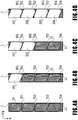
- FIGS. 4A to 4D are views explaining a process for producing the liquid ejection head 13 in the present embodiment. The process proceeds from FIG. 4A to FIG. 4D .
- the base plate 1 comprises flow paths 10 through which the liquid is supplied to the ejection ports 6 from the tank.
Landscapes
- Engineering & Computer Science (AREA)
- Manufacturing & Machinery (AREA)
- Particle Formation And Scattering Control In Inkjet Printers (AREA)
- Ink Jet (AREA)
Abstract
Description
- The present disclosure relates to a liquid ejection head and a process for producing a liquid ejection head.
- Liquid ejection apparatuses such as inkjet printing apparatuses use a liquid ejection head. In the liquid ejection head, a device chip having a plurality of ejection ports is disposed. In recent years, liquid ejection heads in which a plurality of device chips are disposed in a line to achieve a wider print width have been used.
- The specification of
U.S. Patent Laid-Open No. 2011/0020965 (hereinafter referred to as document 1) discloses an IC chip shape to dispose the IC chips of a print head in a line, and a layout of each IC chip and a flow path unit relative to each other. Specifically,document 1 discloses that a plurality of IC chips 100 (The reference numeral indocument 1 is presented. The same applies to the followingsentences describing document 1.) are arrayed in a line with no clearance therebetween, as shown inFIG. 2 ofdocument 1. Also, as shown in FIG. 11 ofdocument 1, indocument 1, the IC chips 100 are positioned using reference marks 103Aon the IC chips 100 and reference marks 103B on a channel molding 124 having a liquid flow path structure. - In
document 1, since the IC chips 100 are arrayed in a line with no clearance therebetween, the reference marks 103B on the channel molding 124, having a liquid flow path structure, cannot be disposed on an array axis extending in the array direction of the plurality of IC chips 100. For this reason, the accuracy of the positioning of the adjacent chips may possibly be lowered. - The present invention in its first aspect provides a liquid ejecting head as specified in
claims 1 to 8. - The present invention in its second aspect provides a process for producing a liquid ejecting head as specified in claims 9 to 11.
- Further features of the present disclosure will become apparent from the following description of exemplary embodiments with reference to the attached drawings.
-
-
FIG. 1 is a perspective view showing an example of a liquid ejection head; -
FIGS. 2A and 2B are views showing an example of device chips; -
FIGS. 3A to 3C are views showing examples of the shape of the device chips; -
FIGS. 4A to 4D are views explaining a process for producing the liquid ejection head; -
FIG. 5 is a view showing an example of device chips; and -
FIG. 6 is a schematic view showing a cross section along line VI-VI. - Embodiments will be described below with reference to the drawings. It is to be noted that the embodiments to be described below are appropriate specific examples and therefore involve various technically preferable limitations. However, the present disclosure is not limited to the embodiments in this specification or other specific methods.
-
FIG. 1 is a perspective view showing an example of aliquid ejection head 13 in the present embodiment. Abase plate 1 has a liquid flow path structure for supplying a liquid (e.g., ink) todevice chips 2 from a tank (not shown). It is preferable that thebase plate 1 be high in chemical resistance and thermal resistance, have insulating properties, and be high in mechanical strength. For example, thebase plate 1 is made of a fine ceramic such as Al2O3 and a plastic such as phenolic resin, polycarbonate resin, or polyphenylene ether resin. - The
device chips 2 are joined in a straight line to the upper surface of thebase plate 1 with an adhesive agent (not shown inFIG. 1). FIG. 1 shows an example in which fourdevice chips 2 are arrayed, but the number of device chips is not limited to four, and the number ofdevice chips 2 may be any number larger than one. Also,first reference marks 7 are provided on the upper surface of thebase plate 1. - Each
device chip 2 comprises asubstrate 3 and an ejectionport forming member 4 on the upper surface of thesubstrate 3. Thedevice chip 2 also compriseselectrical connecting portions 5 and asecond reference mark 8 in a region of the upper surface of thesubstrate 3 where the ejectionport forming member 4 is not provided. A plurality ofejection ports 6 are formed in the ejectionport forming member 4. -
FIGS. 2A and 2B are views explaining thedevice chips 2 in the present embodiment.FIG. 2A is a top view of part A inFIG. 1 .FIG. 2B is a schematic cross-sectional view along line IIB-IIB inFIG. 2A . In eachdevice chip 2, on thesubstrate 3, incorporatingenergy generating elements 12 for ejecting the liquid, there are formed the ejectionport forming member 4 for ejecting the liquid and the electrical connectingportions 5 for driving theenergy generating elements 12. Thesubstrate 3 is made of a semiconductor material such as Si, Ge, SiC, GaAs, InAs, GaP, diamond, ZnO, which is an oxide semiconductor, InN or GaN, which is a nitride semiconductor, a mixture of these or the like, or an organic semiconductor, for example. A publicly known element is usable as eachenergy generating element 12. Examples of the publicly known element include a heater element (heating resistance element), which uses thermal energy, a piezoelectric element, which uses mechanical energy, and so on. In thesubstrate 3, liquid supply ports 9 are formed through which a liquid such as ink is supplied to the ejectionport forming member 4 from thebase plate 1. Examples of the method of forming the liquid supply ports 9 include a method using etching such as dry etching or wet etching or laser ablation or the like to bore holes through thesubstrate 3. The ejectionport forming member 4 has a three-dimensional structure comprising flow paths through which the liquid is caused to flow and theejection ports 6. Examples of the material of the ejectionport forming member 4 include an inorganic material such as Si, SiC, or SiO, and an organic material such as epoxy resin. - The shape of each
device chip 2 is such that a space is formed between theadjacent device chips 2 in the state where they are arrayed. Assume for example a case where a first device chip and a second device chip are arrayed in a line in the array direction in which the device chips are arrayed. Thedevice chips 2 in the present embodiment are shaped such that a clearance is formed at least one region between the first device chip and the second device chip. Forming such a clearance makes part of the surface of thebase plate 1 visible through the clearance in a case where thedevice chips 2 are viewed from their upper surfaces. Thefirst reference marks 7 are disposed on this part of the surface of thebase plate 1. This allows positioning using the reference marks (first reference marks 7) disposed on thebase plate 1. -
FIGS. 3A to 3C are views showing examples of the shape of thedevice chips 2.FIGS. 3A to 3C show examples of the shape of thedevice chips 2 as viewed from their upper surfaces. For example, as shown inFIG. 3A , each derivechip 2 may have the shape of a parallelogram with its acute angle portions cropped. Although each derivechip 2 has the shape of a parallelogram with both acute angle portions cropped inFIG. 3A , the shape may be such that only the acute angle portion on the side where thesecond reference mark 8 is disposed is cropped. As shown inFIG. 3B , each derivechip 2 may have the shape of a trapezoid with its acute angle portions cropped. AlthoughFIG. 3B shows an example where thesecond reference mark 8 is formed at each end in the horizontal direction in the drawing (X direction), thesecond reference mark 8 may be formed only at one end. In this case, the shape may be such that only the acute angle portion on the side where thesecond reference mark 8 is formed is cropped. Thus, the shape of eachdevice chip 2 may be a polygonal shape with five or more corners. - Meanwhile, the shape of the
device chips 2 in the present embodiment only need to be such that a space is formed between the adjacent device chips. Thus, thedevice chips 2 may be device chips of an unsymmetrical irregular shape as shown inFIG. 3C , for example. Moreover, the device chips may have different shapes. Assume also a case where a first device chip, a second device chip, a third device chip, and a fourth device chip are arrayed in this order. In this case, the first and fourth device chips as end sections in the array direction may have different shapes and the second and third device chips as non-end sections may have the same shape. Any shape or shapes may be employed as long as a space is formed between theadjacent device chips 2 in the state where they are arrayed. - Also, the ejection ports are preferably formed such that the ejection ports of the
device chips 2 lying adjacent to each other in the state where thedevice chips 2 are disposed on thebase plate 1 overlap each other in the array direction. In this way, in theliquid ejection head 13 with thedevice chips 2 disposed in the array direction, theejection ports 6 overlap each other in the array direction between the adjacent device chips. Thus, at each region where adjacent device chips lie in proximity to each other, the liquid can be ejected from theejection ports 6 of either device chip. This allows continuous ejection without a break in the array direction. - In the present embodiment, on the
base plate 1, the first reference marks 7 are disposed, which are used for the positioning of thedevice chips 2 in disposing them. The first reference marks 7 are formed along the array axis along which thedevice chips 2 are disposed. The method of forming the first reference marks 7 includes a processing method using mold shaping, laser depiction, or the like in a case where thebase plate 1 is made of a resin material, and a processing method using ultrasonic processing, metal transfer, or the like in a case where thebase plate 1 is made of ceramic. The method only needs to be a processing method capable of accurately marking the first reference marks 7 on thebase plate 1. - In the
liquid ejection head 13 in the present embodiment, the second reference marks 8 on the device chips and the first reference marks 7, present in the spaces formed between the adjacentlydisposed device chips 2, are disposed on the array axis along which the device chips are arrayed. For example, in the present embodiment, the first reference marks 7 are disposed on thebase plate 1 to be located in the spaces formed between the adjacentlydisposed device chips 2. To put it differently, thedevice chips 2 are formed in such a shape(s) so as not to cover the first reference marks 7, which are disposed on thebase plate 1. In sum, the positions on thebase plate 1 where the first reference marks 7 are disposed and the shape(s) of thedevice chips 2 are related to each other. - In the present embodiment, the second reference marks 8 are disposed on the device chips 2. The second reference marks 8 are marks for positioning relative to the first reference marks 7. The second reference marks 8 and the
ejection ports 6 are accurately disposed on thedevice chips 2 since they are patterned by an apparatus for producing semiconductor devices. In theliquid ejection head 13 in the present embodiment, the second reference marks 8 and the first reference marks 7 are disposed on the array axis of the device chips 2. Specifically, the second reference marks 8 on theadjacent device chips 2 and the first reference marks 7 on the base plate are disposed on the array axis of the device chips 2. Also, in the present embodiment, the electrical connectingportions 5 are arrayed on thedevice chips 2 in the array direction of the device chips, and the second reference marks 8 are disposed on the array axis of these electrical connectingportions 5. - Note that the drawings in the present embodiment show an example where the shapes of the first reference marks 7 and the second reference marks 8 are circular shapes, but the shapes are not limited to circular shapes. The shapes may be cross shapes or patterns that are unlikely to be falsely recognized as patterns around them. Also, the shape of the first reference marks 7 and the shape of the second reference marks 8 may be the same shape or different shapes. Further, the plurality of first reference marks 7 may have the same shape or different shapes. Furthermore, the plurality of second reference marks 8 may have the same shape or different shapes.
-
FIGS. 4A to 4D are views explaining a process for producing theliquid ejection head 13 in the present embodiment. The process proceeds fromFIG. 4A to FIG. 4D . Thebase plate 1 comprisesflow paths 10 through which the liquid is supplied to theejection ports 6 from the tank. - As shown in
FIG. 4A , a step of applying anadhesive agent 11 to thebase plate 1 while avoiding reference marks 701, 702, 703, and 704 disposed on thebase plate 1 and theflow paths 10 is performed. Specifically, the amount and the regions in which theadhesive agent 11 is applied are adjusted such that theadhesive agent 11 does not form a link across any of theflow paths 10 or close any of the flow paths. Examples of the method of applying theadhesive agent 11 include a method of applying theadhesive agent 11 with a nozzle dispenser, a roller, a stamper, or the like. Theadhesive agent 11 includes a thermosetting adhesive agent, a UV curable adhesive agent, or the like. - Then, as shown in
FIG. 4B , a step of joining adevice chip 201 to thebase plate 1 in a chip mounter is performed. In doing so, positioning using thereference mark 701 on thebase plate 1 and areference mark 801 on thedevice chip 201 is performed. In the present embodiment, the positioning of thereference mark 701 and thereference mark 801 is performed by image recognition using a camera. Hence, thedevice chip 201 is accurately joined onto theadhesive agent 11. In the present embodiment, for accurate joining, a positioning process is performed within a single screen with a single camera for the image recognition. The positioning needs to be performed such that the liquid supply ports 9 in thesubstrate 3 are positioned on thecorresponding flow paths 10 in thebase plate 1, as shown inFIGS. 2A and 2B . In view of accuracy, it is preferable to dispose thereference mark 701 on thebase plate 1 and thereference mark 801 on thedevice chip 201 such that the reference marks 701 and 801 can be positioned within a close range. As a result, the step of joining thedevice chip 201 at an end section in the array direction is completed, as shown inFIG. 4B . - Then, as shown in
FIG. 4C , a step of joining adevice chip 202 to be adjacent to thedevice chip 201 is performed. Firstly, thedevice chip 202 is picked up. Thereafter, in the chip mounter, thedevice chip 202 is accurately joined by positioning with image recognition performed by detecting areference mark 802 on thedevice chip 202 while detecting thereference mark 702 on thebase plate 1. In view of positioning accuracy, it is preferable to also detect thereference mark 801 on thedevice chip 201 in the present step. In the present production process, the device chips are joined one by one in the chip mounter, but the plurality of device chips may be simultaneously mounted and joined with a plurality of mount fingers in order to increase the throughput. In doing so, a method may be used in which the first reference marks 7 on thebase plate 1 are detected and thedevice chips 2 are positioned simultaneously to shorten the process time. - Then, as shown in
FIG. 4D , like the steps so far, steps of joiningdevice chips base plate 1 in the chip mounter are performed. - Lastly, electric wiring members for driving the energy generating elements are electrically joined (not shown) to the electrical connecting
portions 5 formed on the device chips 201, 202, 203, and 204. As a result, theliquid ejection head 13 is completed. - As described above, the
device chips 2 in the present embodiment are configured in such a shape(s) that a space is formed between the adjacent device chips. Moreover, the first reference marks 7 are disposed on thebase plate 1 at positions corresponding to these spaces. The first reference marks 7 are disposed on an array axis. The second reference marks 8 are disposed on the device chips 2. Further, in joining thedevice chips 2 to thebase plate 1, they are positioned relative to each other on the array axis by using the first reference marks 7 and the second reference marks 8. - In the present embodiment, since the positioning is performed on the array axis by using the first reference marks 7 and the second reference marks 8, as described above, accurate positioning is achieved. By positioning the second reference marks 8 on the device chips relative to the first reference marks 7 on the base plate as in the present embodiment, accurate positioning is achieved as compared to relative positioning in which the second reference marks 8 are positioned relative to each other. Also, by positioning the second reference marks 8 relative to the first reference marks 7, which are disposed on the array axis, accurate positioning without displacement from the axis is achieved as compared to a case where, for example, the reference marks are disposed in a direction orthogonal to the array direction (the width direction of the liquid ejection head 13). Also, since the
device chips 2 in the present embodiment have such a shape(s) that a space is formed between the adjacent device chips, the device chips other than the device chips located at the end sections in the array direction are also positioned relative to the corresponding first reference marks 7, which are disposed on the array axis. Hence, accurate positioning is achieved. - In
embodiment 1, a description has been given a liquid ejection head in which device chips are arrayed in a line in the print width direction (Y axis). Inembodiment 2, a description will be given of a liquid ejection head in which device chips are arrayed in a matrix in both the print width direction (Y axis) and a direction orthogonal to the print width direction (X axis). The production process is substantially the same as that inembodiment 1, and therefore the difference will be mainly described below. -
FIG. 5 is a view explaining the device chips in the present embodiment.Device chips 201 to 209 are joined in a matrix to the upper surface of abase plate 1 with an adhesive agent (not shown inFIG. 5). FIG. 5 shows an example in which nine device chips are disposed on thebase plate 1, but the number of device chips is not limited to nine and may be any number. Each device chip in the present embodiment has such a shape that a space is formed between itself and each of the adjacent chips on the upper, lower, right, and left sides. The method of disposing the device chips onto the base plate is similar to that inembodiment 1. The device chips 201 to 209 in the present embodiment can each be positioned relative to a first reference mark disposed on an array axis in the print width direction (Y axis, first direction) and then further positioned relative to a first reference mark disposed on an X axis (second direction). For example, a plurality of second reference marks are disposed on each device chip. One second reference mark can be positioned relative to the first reference mark disposed on the Y axis on thebase plate 1, and another second reference mark can be positioned relative to the first reference mark disposed on the X axis. Specifically, thedevice chip 205 inFIG. 5 can be positioned using areference mark 805 and areference mark 705 and positioned using areference mark 806 and areference mark 706. - Since the device chips 201 to 209 in the present embodiment are disposed in a matrix, their electrical connecting
portions 5 are configured as back surface electrodes disposed on the back surface sides of the device chips. -
FIG. 6 is a view schematically showing a cross section along line VI-VI inFIG. 5 . The method of disposing the electrical connectingportions 5 on the back surface side of thesubstrate 3 includes a method involving: providing throughholes 17 in thesubstrate 3; forming an insulation layer on the side surfaces of the throughholes 17; and formingplugs 14 as electric wirings in the through holes 17. The method of forming the throughholes 17 includes etching such that drying etching or wet etching, laser ablation, and the like. The insulation layer is made of a film of an oxide such as SiO2 or TiO, for example. The method of forming the insulation layer LP-CVD, which is a chemical vapor deposition method, ALD, which is an atomic deposition method, and the like. Theplugs 14 are made of a metal such as Cu, Al, or Au. The method of forming theplugs 14 includes a method involving: burying their material in the through holes by plating, sputtering, or the like; and then polishing the back face surface side of the substrate by CMP or the like. Prior to forming theplugs 14, a barrier layer to prevent diffusion of Cu may be formed on the insulation film. Depending on the electrical connection, a step of exposing the plug electrodes by performing a thinning process on the back surface by dry etching, wet etching, or the like may be performed. - In electrically joining the device chips, electric wiring members are disposed on the
base plate 1. In order to prevent electric short circuit and the like and avoid contact with a liquid such as ink after the device chips are electrically joined, a sealingagent 15 is injected around the electrical connectingportions 5 from aspace 16 between the adjacent device chips. In doing so, the amount and duration of injection of the sealing agent are adjusted such that the sealing agent does not seal theejection ports 6 inFIGS. 2A and 2B and buries the side surfaces of the adjacent device chips by capillarity. Consequently, the electrical connectingportions 5 are covered with the sealingagent 15. As a result, the liquid ejection head is completed. - As described above, even in the case of producing a liquid ejection head in which device chips are arrayed in a matrix, the device chips are accurately positioned and disposed on a base plate.
- While the present disclosure has been described with reference to exemplary embodiments, it is to be understood that the disclosure is not limited to the disclosed exemplary embodiments. The scope of the following claims is to be accorded the broadest interpretation so as to encompass all such modifications and equivalent structures and functions.
- Provided is a liquid ejection head (13) comprising a base plate (1) and at least two device chips (2) in which ejection ports (6) for ejecting a liquid are formed and which are disposed on the base plate. At least one first reference mark (7) is provided on the base plate. A second reference mark (8) is provided on each of the device chips. At least one space is formed between adjacent ones of the device chips. The second reference marks and the first reference mark present in the space are disposed on an array axis along which the device chips are arrayed.
Claims (11)
- A liquid ejection head (13) comprising a base plate (1) and at least two device chips (2) in which ejection ports (6) for ejecting a liquid are formed, the device chips being disposed on the base plate,
wherein at least one first reference mark (7) is provided on the base plate,
a second reference mark (8) is provided on each of the device chips,
at least one space is formed between adjacent ones of the device chips, and
the second reference marks and the first reference mark present in the space are disposed on an array axis along which the device chips are arrayed. - The liquid ejection head according to claim 1, wherein
each of the device chips has a polygonal shape with at least five corners, and
a space is formed between the adjacent device chips by the polygonal shapes of the device chips. - The liquid ejection head according to claim 1 or 2, wherein the device chips are arrayed in a line on the base plate.
- The liquid ejection head according to any one of claims 1 to 3, wherein
each of the device chips comprises electrical connecting portions, and
the second reference mark on the device chip is disposed on an array axis along which the electrical connecting portions are arrayed. - The liquid ejection head according to any one of claims 1 to 4, wherein each of the device chips includes a region at which the ejection ports of adjacent ones of the device chips overlap each other in an array direction in which the device chips are arrayed.
- The liquid ejection head according to claim 1 or 2, wherein the device chips are disposed on the base plate in a matrix in a first direction and a second direction crossing the first direction.
- The liquid ejection head according to claim 6, wherein
each of the device chips comprises a plurality of the second reference marks, and
the plurality of second reference marks includea reference mark disposed on an axis in the first direction relative to the first reference mark present in the space in the first direction, anda reference mark disposed on an axis in the second direction relative to the first reference mark present in the space in the second direction. - The liquid ejection head according to claim 6 or 7, wherein
each of the device chips comprises an electrical connecting portion on a back surface of a substrate of the device chip, and
the spaces are filled with a sealing agent for covering the electrical connecting portions. - A process for producing a liquid ejection head (13) comprising a base plate (1) and at least two device chips (2) in which ejection ports (6) for ejecting a liquid are formed, the device chips being disposed on the base plate, the process comprising:applying an adhesive agent (11) onto the base plate with at least one first reference (7) mark provided thereon; andjoining each of the device chips with a second reference mark (8) provided thereon onto the base plate with the adhesive agent applied thereto,wherein at least one space is formed between adjacent ones of the joined device chips, andthe second reference marks and the first reference mark present in the space are disposed on an array axis along which the device chips are arrayed.
- The process for producing a liquid ejection head according to claim 9, wherein the joining includes simultaneously joining at least two of the device chips onto the base plate.
- The process for producing a liquid ejection head according to claim 9 or 10, wherein
an electrical connecting portion is provided on a back surface of a substrate of each of the device chips, and
the method further comprises injecting a sealing agent for covering the electrical connecting portion into the space.
Applications Claiming Priority (1)
| Application Number | Priority Date | Filing Date | Title |
|---|---|---|---|
| JP2018166888A JP7154897B2 (en) | 2018-09-06 | 2018-09-06 | LIQUID EJECTION HEAD AND METHOD FOR MANUFACTURING LIQUID EJECTION HEAD |
Publications (2)
| Publication Number | Publication Date |
|---|---|
| EP3620303A1 true EP3620303A1 (en) | 2020-03-11 |
| EP3620303B1 EP3620303B1 (en) | 2022-04-20 |
Family
ID=67620293
Family Applications (1)
| Application Number | Title | Priority Date | Filing Date |
|---|---|---|---|
| EP19191399.5A Active EP3620303B1 (en) | 2018-09-06 | 2019-08-13 | Liquid ejection head and process for producing liquid ejection head |
Country Status (4)
| Country | Link |
|---|---|
| US (5) | US11097540B2 (en) |
| EP (1) | EP3620303B1 (en) |
| JP (1) | JP7154897B2 (en) |
| CN (1) | CN110877486B (en) |
Families Citing this family (9)
| Publication number | Priority date | Publication date | Assignee | Title |
|---|---|---|---|---|
| JP7491074B2 (en) | 2020-06-17 | 2024-05-28 | セイコーエプソン株式会社 | LIQUID EJECT HEAD AND LIQUID EJECT APPARATUS |
| JP7552151B2 (en) | 2020-08-31 | 2024-09-18 | セイコーエプソン株式会社 | LIQUID EJECTION APPARATUS, HEAD DRIVE CIRCUIT, AND LIQUID EJECTION HEAD |
| CN113752691B (en) * | 2020-06-01 | 2025-07-22 | 精工爱普生株式会社 | Liquid ejecting head and liquid ejecting apparatus |
| US11760093B2 (en) | 2020-06-01 | 2023-09-19 | Seiko Epson Corporation | Liquid ejecting head and liquid ejecting apparatus |
| JP7552118B2 (en) | 2020-07-27 | 2024-09-18 | セイコーエプソン株式会社 | Liquid ejection head and liquid ejection apparatus |
| JP2021187075A (en) | 2020-06-01 | 2021-12-13 | セイコーエプソン株式会社 | Liquid injection head and liquid injection device |
| JP7631991B2 (en) | 2020-06-17 | 2025-02-19 | セイコーエプソン株式会社 | Flow path member, liquid ejection head, liquid ejection device, and method for manufacturing flow path member |
| MX2023009977A (en) * | 2021-03-26 | 2023-09-06 | Sekisui Chemical Co Ltd | Ink-jet adhesive, method for producing electronic component, and electronic component. |
| JP2024049554A (en) * | 2022-09-29 | 2024-04-10 | キヤノン株式会社 | Liquid ejection head and recording apparatus |
Citations (3)
| Publication number | Priority date | Publication date | Assignee | Title |
|---|---|---|---|---|
| US6350013B1 (en) * | 1997-10-28 | 2002-02-26 | Hewlett-Packard Company | Carrier positioning for wide-array inkjet printhead assembly |
| US20100046007A1 (en) * | 2008-08-19 | 2010-02-25 | Silverbrook Research Pty Ltd | Measuring apparatus for performing positional analysis on an integrated circuit carrier |
| US20110020965A1 (en) | 2009-07-27 | 2011-01-27 | Silverbrook Research Pty Ltd | Method of fabricating printhead integrated circuit with backside electrical connections |
Family Cites Families (34)
| Publication number | Priority date | Publication date | Assignee | Title |
|---|---|---|---|---|
| JPS59164161A (en) * | 1983-03-09 | 1984-09-17 | Mitsubishi Electric Corp | Light emitting diode array head |
| GB2210500A (en) * | 1987-09-30 | 1989-06-07 | Plessey Co Plc | Method of alignment of led chips |
| US5198054A (en) * | 1991-08-12 | 1993-03-30 | Xerox Corporation | Method of making compensated collinear reading or writing bar arrays assembled from subunits |
| US6137506A (en) * | 1994-06-13 | 2000-10-24 | Canon Kabushiki Kaisha | Ink jet recording head with a plurality of orifice plates |
| US6165813A (en) * | 1995-04-03 | 2000-12-26 | Xerox Corporation | Replacing semiconductor chips in a full-width chip array |
| JP3503677B2 (en) * | 1997-02-19 | 2004-03-08 | キヤノン株式会社 | Wiring board connection method and wiring board connection device |
| JP3700702B2 (en) | 2003-01-06 | 2005-09-28 | セイコーエプソン株式会社 | Liquid jet head |
| KR20050039623A (en) | 2003-10-24 | 2005-04-29 | 소니 가부시끼 가이샤 | Head module, liquid ejecting head, liquid ejecting apparatus, manufacturing method of head module and manufacturing method of liquid ejecting head |
| JP4192830B2 (en) | 2004-04-27 | 2008-12-10 | ブラザー工業株式会社 | Wiring member connection method |
| JP5032752B2 (en) * | 2005-06-03 | 2012-09-26 | キヤノン株式会社 | Inkjet recording apparatus and inkjet recording method |
| US7465033B2 (en) * | 2005-12-05 | 2008-12-16 | Silverbrook Research Ptv Ltd | Self-referencing printhead assembly |
| JP4827668B2 (en) * | 2006-09-11 | 2011-11-30 | 富士フイルム株式会社 | Liquid discharge head and method of manufacturing liquid discharge head |
| JP4293220B2 (en) | 2006-09-29 | 2009-07-08 | ブラザー工業株式会社 | Liquid ejector |
| JP4876839B2 (en) | 2006-10-12 | 2012-02-15 | 富士ゼロックス株式会社 | Droplet discharge head, manufacturing method thereof, and droplet discharge apparatus |
| CN100515778C (en) | 2007-03-09 | 2009-07-22 | 北京美科艺数码科技发展有限公司 | Spray head adjustment mechanism, its adjustment method, and equipment using the print head adjustment mechanism |
| US7583284B2 (en) * | 2008-01-29 | 2009-09-01 | Universal Scientific Industrial Co., Ltd. | Method for arranging print head chips |
| CN101498784A (en) * | 2008-02-01 | 2009-08-05 | 韩国科亚电子股份有限公司 | Apparatus and method for tracking satellite signal |
| JP4557027B2 (en) * | 2008-03-13 | 2010-10-06 | ブラザー工業株式会社 | Recording device |
| JP4720917B2 (en) | 2009-03-02 | 2011-07-13 | ブラザー工業株式会社 | LIQUID DISCHARGE HEAD, RECORDING DEVICE MANUFACTURING METHOD INCLUDING THE SAME, LIQUID DISCHARGE HEAD AND RECORDING DEVICE |
| JP6024076B2 (en) | 2011-01-13 | 2016-11-09 | セイコーエプソン株式会社 | Manufacturing method of silicon device |
| TWI530402B (en) * | 2011-09-21 | 2016-04-21 | 滿捷特科技公司 | Printer for minimizing adverse mixing of high and low luminance inks at nozzle face of inkjet printhead |
| JP6238617B2 (en) * | 2013-07-24 | 2017-11-29 | キヤノン株式会社 | Liquid discharge head and liquid discharge apparatus |
| JP6075558B2 (en) * | 2013-08-20 | 2017-02-08 | セイコーエプソン株式会社 | Method for manufacturing liquid jet head |
| JP6217914B2 (en) | 2013-12-06 | 2017-10-25 | セイコーエプソン株式会社 | Liquid ejecting head, liquid ejecting head unit, and liquid ejecting apparatus |
| JP6323655B2 (en) * | 2014-01-14 | 2018-05-16 | セイコーエプソン株式会社 | Liquid ejecting head, liquid ejecting head unit, liquid ejecting line head, and liquid ejecting apparatus |
| JP6422366B2 (en) | 2014-05-13 | 2018-11-14 | キヤノン株式会社 | Liquid ejection head and recording apparatus |
| WO2016043303A1 (en) * | 2014-09-19 | 2016-03-24 | コニカミノルタ株式会社 | Inkjet head, inkjet head module, and inkjet printer |
| JP5960325B1 (en) | 2015-06-03 | 2016-08-02 | キヤノン株式会社 | Method for manufacturing liquid discharge head |
| JP6840959B2 (en) | 2015-11-18 | 2021-03-10 | 株式会社リコー | Head unit, device that discharges liquid |
| US9895892B2 (en) * | 2015-11-18 | 2018-02-20 | Ricoh Company, Ltd. | Head unit and liquid discharge apparatus including same |
| JP6790419B2 (en) | 2016-03-31 | 2020-11-25 | ブラザー工業株式会社 | Head unit and liquid discharge device |
| US10272672B2 (en) | 2016-12-22 | 2019-04-30 | Seiko Epson Corporation | Head unit, liquid discharge apparatus, and manufacturing method of head unit |
| JP2019089223A (en) * | 2017-11-13 | 2019-06-13 | エスアイアイ・プリンテック株式会社 | Liquid jet head, and liquid jet recording device |
| US10336074B1 (en) * | 2018-01-18 | 2019-07-02 | Rf Printing Technologies | Inkjet printhead with hierarchically aligned printhead units |
-
2018
- 2018-09-06 JP JP2018166888A patent/JP7154897B2/en active Active
-
2019
- 2019-08-09 US US16/536,675 patent/US11097540B2/en active Active
- 2019-08-13 EP EP19191399.5A patent/EP3620303B1/en active Active
- 2019-09-03 CN CN201910825030.9A patent/CN110877486B/en active Active
-
2021
- 2021-08-03 US US17/392,419 patent/US11938729B2/en active Active
-
2023
- 2023-11-22 US US18/517,459 patent/US12162283B2/en active Active
- 2023-11-22 US US18/517,965 patent/US12005708B2/en active Active
-
2024
- 2024-11-19 US US18/952,332 patent/US20250074055A1/en active Pending
Patent Citations (3)
| Publication number | Priority date | Publication date | Assignee | Title |
|---|---|---|---|---|
| US6350013B1 (en) * | 1997-10-28 | 2002-02-26 | Hewlett-Packard Company | Carrier positioning for wide-array inkjet printhead assembly |
| US20100046007A1 (en) * | 2008-08-19 | 2010-02-25 | Silverbrook Research Pty Ltd | Measuring apparatus for performing positional analysis on an integrated circuit carrier |
| US20110020965A1 (en) | 2009-07-27 | 2011-01-27 | Silverbrook Research Pty Ltd | Method of fabricating printhead integrated circuit with backside electrical connections |
Also Published As
| Publication number | Publication date |
|---|---|
| US20240092080A1 (en) | 2024-03-21 |
| EP3620303B1 (en) | 2022-04-20 |
| US11097540B2 (en) | 2021-08-24 |
| US11938729B2 (en) | 2024-03-26 |
| US12005708B2 (en) | 2024-06-11 |
| CN110877486B (en) | 2021-10-29 |
| US20210362499A1 (en) | 2021-11-25 |
| US20200079086A1 (en) | 2020-03-12 |
| US20250074055A1 (en) | 2025-03-06 |
| US20240083167A1 (en) | 2024-03-14 |
| JP2020040223A (en) | 2020-03-19 |
| US12162283B2 (en) | 2024-12-10 |
| JP7154897B2 (en) | 2022-10-18 |
| CN110877486A (en) | 2020-03-13 |
Similar Documents
| Publication | Publication Date | Title |
|---|---|---|
| US12162283B2 (en) | Liquid ejection head and process for producing liquid ejection head | |
| CN106457861B (en) | Method for making molded device assembly and printhead assembly | |
| CN105793044B (en) | Printhead with bond pads surrounded by dams | |
| US7673971B2 (en) | Fluid ejection device and manufacturing method | |
| US7980676B2 (en) | Liquid ejection head including member supporting liquid ejection substrate | |
| CN108349254B (en) | Printing head | |
| JP5475116B2 (en) | Inkjet printhead assembly and printhead integrated circuit | |
| US20120325772A1 (en) | Ink-jet recording head, recording element substrate, method for manufacturing ink-jet recording head, and method for manufacturing recording element substrate | |
| JP5995718B2 (en) | Head chip, head chip manufacturing method, liquid ejecting head, and liquid ejecting apparatus | |
| US8342655B2 (en) | Liquid jet head and method for manufacturing liquid jet head | |
| US8100508B2 (en) | Ink jet printing head | |
| CN107531052B (en) | fluid ejection equipment | |
| JP7739131B2 (en) | Liquid ejection head and manufacturing method thereof | |
| US8152278B2 (en) | Liquid jet head chip and manufacturing method therefor | |
| US8197030B1 (en) | Fluid ejector structure | |
| JP2008162110A (en) | Inkjet head, manufacturing method for inkjet head and wiring substrate for mounting head chip | |
| JP7346150B2 (en) | Inkjet recording head and inkjet recording device | |
| TWI492851B (en) | Printhead integrated comprising through-silicon connectors | |
| TWI495570B (en) | Inkjet printhead assembly having backside electrical connection | |
| US10052870B2 (en) | Liquid supply substrate, method of producing the same, and liquid ejecting head |
Legal Events
| Date | Code | Title | Description |
|---|---|---|---|
| PUAI | Public reference made under article 153(3) epc to a published international application that has entered the european phase |
Free format text: ORIGINAL CODE: 0009012 |
|
| STAA | Information on the status of an ep patent application or granted ep patent |
Free format text: STATUS: THE APPLICATION HAS BEEN PUBLISHED |
|
| AK | Designated contracting states |
Kind code of ref document: A1 Designated state(s): AL AT BE BG CH CY CZ DE DK EE ES FI FR GB GR HR HU IE IS IT LI LT LU LV MC MK MT NL NO PL PT RO RS SE SI SK SM TR |
|
| AX | Request for extension of the european patent |
Extension state: BA ME |
|
| STAA | Information on the status of an ep patent application or granted ep patent |
Free format text: STATUS: REQUEST FOR EXAMINATION WAS MADE |
|
| 17P | Request for examination filed |
Effective date: 20200911 |
|
| RBV | Designated contracting states (corrected) |
Designated state(s): AL AT BE BG CH CY CZ DE DK EE ES FI FR GB GR HR HU IE IS IT LI LT LU LV MC MK MT NL NO PL PT RO RS SE SI SK SM TR |
|
| GRAP | Despatch of communication of intention to grant a patent |
Free format text: ORIGINAL CODE: EPIDOSNIGR1 |
|
| STAA | Information on the status of an ep patent application or granted ep patent |
Free format text: STATUS: GRANT OF PATENT IS INTENDED |
|
| INTG | Intention to grant announced |
Effective date: 20211108 |
|
| RIC1 | Information provided on ipc code assigned before grant |
Ipc: B41J 2/14 20060101AFI20211025BHEP |
|
| GRAS | Grant fee paid |
Free format text: ORIGINAL CODE: EPIDOSNIGR3 |
|
| GRAA | (expected) grant |
Free format text: ORIGINAL CODE: 0009210 |
|
| STAA | Information on the status of an ep patent application or granted ep patent |
Free format text: STATUS: THE PATENT HAS BEEN GRANTED |
|
| AK | Designated contracting states |
Kind code of ref document: B1 Designated state(s): AL AT BE BG CH CY CZ DE DK EE ES FI FR GB GR HR HU IE IS IT LI LT LU LV MC MK MT NL NO PL PT RO RS SE SI SK SM TR |
|
| REG | Reference to a national code |
Ref country code: GB Ref legal event code: FG4D |
|
| REG | Reference to a national code |
Ref country code: CH Ref legal event code: EP |
|
| REG | Reference to a national code |
Ref country code: IE Ref legal event code: FG4D |
|
| REG | Reference to a national code |
Ref country code: DE Ref legal event code: R096 Ref document number: 602019013835 Country of ref document: DE |
|
| REG | Reference to a national code |
Ref country code: AT Ref legal event code: REF Ref document number: 1484884 Country of ref document: AT Kind code of ref document: T Effective date: 20220515 |
|
| REG | Reference to a national code |
Ref country code: LT Ref legal event code: MG9D |
|
| REG | Reference to a national code |
Ref country code: NL Ref legal event code: MP Effective date: 20220420 |
|
| REG | Reference to a national code |
Ref country code: AT Ref legal event code: MK05 Ref document number: 1484884 Country of ref document: AT Kind code of ref document: T Effective date: 20220420 |
|
| PG25 | Lapsed in a contracting state [announced via postgrant information from national office to epo] |
Ref country code: NL Free format text: LAPSE BECAUSE OF FAILURE TO SUBMIT A TRANSLATION OF THE DESCRIPTION OR TO PAY THE FEE WITHIN THE PRESCRIBED TIME-LIMIT Effective date: 20220420 |
|
| PG25 | Lapsed in a contracting state [announced via postgrant information from national office to epo] |
Ref country code: SE Free format text: LAPSE BECAUSE OF FAILURE TO SUBMIT A TRANSLATION OF THE DESCRIPTION OR TO PAY THE FEE WITHIN THE PRESCRIBED TIME-LIMIT Effective date: 20220420 Ref country code: PT Free format text: LAPSE BECAUSE OF FAILURE TO SUBMIT A TRANSLATION OF THE DESCRIPTION OR TO PAY THE FEE WITHIN THE PRESCRIBED TIME-LIMIT Effective date: 20220822 Ref country code: NO Free format text: LAPSE BECAUSE OF FAILURE TO SUBMIT A TRANSLATION OF THE DESCRIPTION OR TO PAY THE FEE WITHIN THE PRESCRIBED TIME-LIMIT Effective date: 20220720 Ref country code: LT Free format text: LAPSE BECAUSE OF FAILURE TO SUBMIT A TRANSLATION OF THE DESCRIPTION OR TO PAY THE FEE WITHIN THE PRESCRIBED TIME-LIMIT Effective date: 20220420 Ref country code: HR Free format text: LAPSE BECAUSE OF FAILURE TO SUBMIT A TRANSLATION OF THE DESCRIPTION OR TO PAY THE FEE WITHIN THE PRESCRIBED TIME-LIMIT Effective date: 20220420 Ref country code: GR Free format text: LAPSE BECAUSE OF FAILURE TO SUBMIT A TRANSLATION OF THE DESCRIPTION OR TO PAY THE FEE WITHIN THE PRESCRIBED TIME-LIMIT Effective date: 20220721 Ref country code: FI Free format text: LAPSE BECAUSE OF FAILURE TO SUBMIT A TRANSLATION OF THE DESCRIPTION OR TO PAY THE FEE WITHIN THE PRESCRIBED TIME-LIMIT Effective date: 20220420 Ref country code: ES Free format text: LAPSE BECAUSE OF FAILURE TO SUBMIT A TRANSLATION OF THE DESCRIPTION OR TO PAY THE FEE WITHIN THE PRESCRIBED TIME-LIMIT Effective date: 20220420 Ref country code: BG Free format text: LAPSE BECAUSE OF FAILURE TO SUBMIT A TRANSLATION OF THE DESCRIPTION OR TO PAY THE FEE WITHIN THE PRESCRIBED TIME-LIMIT Effective date: 20220720 Ref country code: AT Free format text: LAPSE BECAUSE OF FAILURE TO SUBMIT A TRANSLATION OF THE DESCRIPTION OR TO PAY THE FEE WITHIN THE PRESCRIBED TIME-LIMIT Effective date: 20220420 |
|
| PG25 | Lapsed in a contracting state [announced via postgrant information from national office to epo] |
Ref country code: RS Free format text: LAPSE BECAUSE OF FAILURE TO SUBMIT A TRANSLATION OF THE DESCRIPTION OR TO PAY THE FEE WITHIN THE PRESCRIBED TIME-LIMIT Effective date: 20220420 Ref country code: PL Free format text: LAPSE BECAUSE OF FAILURE TO SUBMIT A TRANSLATION OF THE DESCRIPTION OR TO PAY THE FEE WITHIN THE PRESCRIBED TIME-LIMIT Effective date: 20220420 Ref country code: LV Free format text: LAPSE BECAUSE OF FAILURE TO SUBMIT A TRANSLATION OF THE DESCRIPTION OR TO PAY THE FEE WITHIN THE PRESCRIBED TIME-LIMIT Effective date: 20220420 Ref country code: IS Free format text: LAPSE BECAUSE OF FAILURE TO SUBMIT A TRANSLATION OF THE DESCRIPTION OR TO PAY THE FEE WITHIN THE PRESCRIBED TIME-LIMIT Effective date: 20220820 |
|
| REG | Reference to a national code |
Ref country code: DE Ref legal event code: R097 Ref document number: 602019013835 Country of ref document: DE |
|
| PG25 | Lapsed in a contracting state [announced via postgrant information from national office to epo] |
Ref country code: SM Free format text: LAPSE BECAUSE OF FAILURE TO SUBMIT A TRANSLATION OF THE DESCRIPTION OR TO PAY THE FEE WITHIN THE PRESCRIBED TIME-LIMIT Effective date: 20220420 Ref country code: SK Free format text: LAPSE BECAUSE OF FAILURE TO SUBMIT A TRANSLATION OF THE DESCRIPTION OR TO PAY THE FEE WITHIN THE PRESCRIBED TIME-LIMIT Effective date: 20220420 Ref country code: RO Free format text: LAPSE BECAUSE OF FAILURE TO SUBMIT A TRANSLATION OF THE DESCRIPTION OR TO PAY THE FEE WITHIN THE PRESCRIBED TIME-LIMIT Effective date: 20220420 Ref country code: EE Free format text: LAPSE BECAUSE OF FAILURE TO SUBMIT A TRANSLATION OF THE DESCRIPTION OR TO PAY THE FEE WITHIN THE PRESCRIBED TIME-LIMIT Effective date: 20220420 Ref country code: DK Free format text: LAPSE BECAUSE OF FAILURE TO SUBMIT A TRANSLATION OF THE DESCRIPTION OR TO PAY THE FEE WITHIN THE PRESCRIBED TIME-LIMIT Effective date: 20220420 Ref country code: CZ Free format text: LAPSE BECAUSE OF FAILURE TO SUBMIT A TRANSLATION OF THE DESCRIPTION OR TO PAY THE FEE WITHIN THE PRESCRIBED TIME-LIMIT Effective date: 20220420 |
|
| PLBE | No opposition filed within time limit |
Free format text: ORIGINAL CODE: 0009261 |
|
| STAA | Information on the status of an ep patent application or granted ep patent |
Free format text: STATUS: NO OPPOSITION FILED WITHIN TIME LIMIT |
|
| 26N | No opposition filed |
Effective date: 20230123 |
|
| PG25 | Lapsed in a contracting state [announced via postgrant information from national office to epo] |
Ref country code: MC Free format text: LAPSE BECAUSE OF FAILURE TO SUBMIT A TRANSLATION OF THE DESCRIPTION OR TO PAY THE FEE WITHIN THE PRESCRIBED TIME-LIMIT Effective date: 20220420 Ref country code: AL Free format text: LAPSE BECAUSE OF FAILURE TO SUBMIT A TRANSLATION OF THE DESCRIPTION OR TO PAY THE FEE WITHIN THE PRESCRIBED TIME-LIMIT Effective date: 20220420 |
|
| REG | Reference to a national code |
Ref country code: CH Ref legal event code: PL |
|
| PG25 | Lapsed in a contracting state [announced via postgrant information from national office to epo] |
Ref country code: LU Free format text: LAPSE BECAUSE OF NON-PAYMENT OF DUE FEES Effective date: 20220813 Ref country code: LI Free format text: LAPSE BECAUSE OF NON-PAYMENT OF DUE FEES Effective date: 20220831 Ref country code: CH Free format text: LAPSE BECAUSE OF NON-PAYMENT OF DUE FEES Effective date: 20220831 |
|
| REG | Reference to a national code |
Ref country code: BE Ref legal event code: MM Effective date: 20220831 |
|
| PG25 | Lapsed in a contracting state [announced via postgrant information from national office to epo] |
Ref country code: SI Free format text: LAPSE BECAUSE OF FAILURE TO SUBMIT A TRANSLATION OF THE DESCRIPTION OR TO PAY THE FEE WITHIN THE PRESCRIBED TIME-LIMIT Effective date: 20220420 |
|
| PG25 | Lapsed in a contracting state [announced via postgrant information from national office to epo] |
Ref country code: IE Free format text: LAPSE BECAUSE OF NON-PAYMENT OF DUE FEES Effective date: 20220813 Ref country code: FR Free format text: LAPSE BECAUSE OF NON-PAYMENT OF DUE FEES Effective date: 20220831 |
|
| PG25 | Lapsed in a contracting state [announced via postgrant information from national office to epo] |
Ref country code: BE Free format text: LAPSE BECAUSE OF NON-PAYMENT OF DUE FEES Effective date: 20220831 |
|
| PG25 | Lapsed in a contracting state [announced via postgrant information from national office to epo] |
Ref country code: IT Free format text: LAPSE BECAUSE OF FAILURE TO SUBMIT A TRANSLATION OF THE DESCRIPTION OR TO PAY THE FEE WITHIN THE PRESCRIBED TIME-LIMIT Effective date: 20220420 |
|
| PG25 | Lapsed in a contracting state [announced via postgrant information from national office to epo] |
Ref country code: HU Free format text: LAPSE BECAUSE OF FAILURE TO SUBMIT A TRANSLATION OF THE DESCRIPTION OR TO PAY THE FEE WITHIN THE PRESCRIBED TIME-LIMIT; INVALID AB INITIO Effective date: 20190813 |
|
| GBPC | Gb: european patent ceased through non-payment of renewal fee |
Effective date: 20230813 |
|
| PG25 | Lapsed in a contracting state [announced via postgrant information from national office to epo] |
Ref country code: CY Free format text: LAPSE BECAUSE OF FAILURE TO SUBMIT A TRANSLATION OF THE DESCRIPTION OR TO PAY THE FEE WITHIN THE PRESCRIBED TIME-LIMIT Effective date: 20220420 |
|
| PG25 | Lapsed in a contracting state [announced via postgrant information from national office to epo] |
Ref country code: MK Free format text: LAPSE BECAUSE OF FAILURE TO SUBMIT A TRANSLATION OF THE DESCRIPTION OR TO PAY THE FEE WITHIN THE PRESCRIBED TIME-LIMIT Effective date: 20220420 |
|
| PG25 | Lapsed in a contracting state [announced via postgrant information from national office to epo] |
Ref country code: GB Free format text: LAPSE BECAUSE OF NON-PAYMENT OF DUE FEES Effective date: 20230813 |
|
| PG25 | Lapsed in a contracting state [announced via postgrant information from national office to epo] |
Ref country code: GB Free format text: LAPSE BECAUSE OF NON-PAYMENT OF DUE FEES Effective date: 20230813 |
|
| PG25 | Lapsed in a contracting state [announced via postgrant information from national office to epo] |
Ref country code: MT Free format text: LAPSE BECAUSE OF FAILURE TO SUBMIT A TRANSLATION OF THE DESCRIPTION OR TO PAY THE FEE WITHIN THE PRESCRIBED TIME-LIMIT Effective date: 20220420 |
|
| PG25 | Lapsed in a contracting state [announced via postgrant information from national office to epo] |
Ref country code: BG Free format text: LAPSE BECAUSE OF FAILURE TO SUBMIT A TRANSLATION OF THE DESCRIPTION OR TO PAY THE FEE WITHIN THE PRESCRIBED TIME-LIMIT Effective date: 20220420 |
|
| PG25 | Lapsed in a contracting state [announced via postgrant information from national office to epo] |
Ref country code: BG Free format text: LAPSE BECAUSE OF FAILURE TO SUBMIT A TRANSLATION OF THE DESCRIPTION OR TO PAY THE FEE WITHIN THE PRESCRIBED TIME-LIMIT Effective date: 20220420 |
|
| PGFP | Annual fee paid to national office [announced via postgrant information from national office to epo] |
Ref country code: DE Payment date: 20250724 Year of fee payment: 7 |
|
| PG25 | Lapsed in a contracting state [announced via postgrant information from national office to epo] |
Ref country code: TR Free format text: LAPSE BECAUSE OF FAILURE TO SUBMIT A TRANSLATION OF THE DESCRIPTION OR TO PAY THE FEE WITHIN THE PRESCRIBED TIME-LIMIT Effective date: 20220420 |