EP3619614B1 - Cache coherent node controller for scale-up shared memory systems - Google Patents
Cache coherent node controller for scale-up shared memory systems Download PDFInfo
- Publication number
- EP3619614B1 EP3619614B1 EP18730137.9A EP18730137A EP3619614B1 EP 3619614 B1 EP3619614 B1 EP 3619614B1 EP 18730137 A EP18730137 A EP 18730137A EP 3619614 B1 EP3619614 B1 EP 3619614B1
- Authority
- EP
- European Patent Office
- Prior art keywords
- node controller
- memory
- fpga
- cpu
- fpga node
- Prior art date
- Legal status (The legal status is an assumption and is not a legal conclusion. Google has not performed a legal analysis and makes no representation as to the accuracy of the status listed.)
- Active
Links
Images

Classifications
-
- G—PHYSICS
- G06—COMPUTING OR CALCULATING; COUNTING
- G06F—ELECTRIC DIGITAL DATA PROCESSING
- G06F12/00—Accessing, addressing or allocating within memory systems or architectures
- G06F12/02—Addressing or allocation; Relocation
- G06F12/08—Addressing or allocation; Relocation in hierarchically structured memory systems, e.g. virtual memory systems
- G06F12/0802—Addressing of a memory level in which the access to the desired data or data block requires associative addressing means, e.g. caches
- G06F12/0806—Multiuser, multiprocessor or multiprocessing cache systems
- G06F12/0815—Cache consistency protocols
- G06F12/0817—Cache consistency protocols using directory methods
- G06F12/0828—Cache consistency protocols using directory methods with concurrent directory accessing, i.e. handling multiple concurrent coherency transactions
-
- G—PHYSICS
- G06—COMPUTING OR CALCULATING; COUNTING
- G06F—ELECTRIC DIGITAL DATA PROCESSING
- G06F12/00—Accessing, addressing or allocating within memory systems or architectures
-
- G—PHYSICS
- G06—COMPUTING OR CALCULATING; COUNTING
- G06F—ELECTRIC DIGITAL DATA PROCESSING
- G06F12/00—Accessing, addressing or allocating within memory systems or architectures
- G06F12/02—Addressing or allocation; Relocation
- G06F12/08—Addressing or allocation; Relocation in hierarchically structured memory systems, e.g. virtual memory systems
- G06F12/0802—Addressing of a memory level in which the access to the desired data or data block requires associative addressing means, e.g. caches
- G06F12/0806—Multiuser, multiprocessor or multiprocessing cache systems
- G06F12/0811—Multiuser, multiprocessor or multiprocessing cache systems with multilevel cache hierarchies
-
- G—PHYSICS
- G06—COMPUTING OR CALCULATING; COUNTING
- G06F—ELECTRIC DIGITAL DATA PROCESSING
- G06F12/00—Accessing, addressing or allocating within memory systems or architectures
- G06F12/02—Addressing or allocation; Relocation
- G06F12/08—Addressing or allocation; Relocation in hierarchically structured memory systems, e.g. virtual memory systems
- G06F12/0802—Addressing of a memory level in which the access to the desired data or data block requires associative addressing means, e.g. caches
- G06F12/0806—Multiuser, multiprocessor or multiprocessing cache systems
- G06F12/0813—Multiuser, multiprocessor or multiprocessing cache systems with a network or matrix configuration
-
- G—PHYSICS
- G06—COMPUTING OR CALCULATING; COUNTING
- G06F—ELECTRIC DIGITAL DATA PROCESSING
- G06F12/00—Accessing, addressing or allocating within memory systems or architectures
- G06F12/02—Addressing or allocation; Relocation
- G06F12/08—Addressing or allocation; Relocation in hierarchically structured memory systems, e.g. virtual memory systems
- G06F12/0802—Addressing of a memory level in which the access to the desired data or data block requires associative addressing means, e.g. caches
- G06F12/0806—Multiuser, multiprocessor or multiprocessing cache systems
- G06F12/0815—Cache consistency protocols
- G06F12/0817—Cache consistency protocols using directory methods
- G06F12/0822—Copy directories
-
- G—PHYSICS
- G06—COMPUTING OR CALCULATING; COUNTING
- G06F—ELECTRIC DIGITAL DATA PROCESSING
- G06F12/00—Accessing, addressing or allocating within memory systems or architectures
- G06F12/02—Addressing or allocation; Relocation
- G06F12/08—Addressing or allocation; Relocation in hierarchically structured memory systems, e.g. virtual memory systems
- G06F12/0802—Addressing of a memory level in which the access to the desired data or data block requires associative addressing means, e.g. caches
- G06F12/0806—Multiuser, multiprocessor or multiprocessing cache systems
- G06F12/0815—Cache consistency protocols
- G06F12/0817—Cache consistency protocols using directory methods
- G06F12/0826—Limited pointers directories; State-only directories without pointers
-
- G—PHYSICS
- G06—COMPUTING OR CALCULATING; COUNTING
- G06F—ELECTRIC DIGITAL DATA PROCESSING
- G06F13/00—Interconnection of, or transfer of information or other signals between, memories, input/output devices or central processing units
- G06F13/38—Information transfer, e.g. on bus
- G06F13/40—Bus structure
- G06F13/4004—Coupling between buses
- G06F13/4009—Coupling between buses with data restructuring
- G06F13/4018—Coupling between buses with data restructuring with data-width conversion
-
- G—PHYSICS
- G06—COMPUTING OR CALCULATING; COUNTING
- G06F—ELECTRIC DIGITAL DATA PROCESSING
- G06F13/00—Interconnection of, or transfer of information or other signals between, memories, input/output devices or central processing units
- G06F13/38—Information transfer, e.g. on bus
- G06F13/40—Bus structure
- G06F13/4004—Coupling between buses
- G06F13/4022—Coupling between buses using switching circuits, e.g. switching matrix, connection or expansion network
-
- G—PHYSICS
- G06—COMPUTING OR CALCULATING; COUNTING
- G06F—ELECTRIC DIGITAL DATA PROCESSING
- G06F15/00—Digital computers in general; Data processing equipment in general
- G06F15/16—Combinations of two or more digital computers each having at least an arithmetic unit, a program unit and a register, e.g. for a simultaneous processing of several programs
-
- G—PHYSICS
- G06—COMPUTING OR CALCULATING; COUNTING
- G06F—ELECTRIC DIGITAL DATA PROCESSING
- G06F15/00—Digital computers in general; Data processing equipment in general
- G06F15/16—Combinations of two or more digital computers each having at least an arithmetic unit, a program unit and a register, e.g. for a simultaneous processing of several programs
- G06F15/163—Interprocessor communication
- G06F15/173—Interprocessor communication using an interconnection network, e.g. matrix, shuffle, pyramid, star, snowflake
-
- G—PHYSICS
- G06—COMPUTING OR CALCULATING; COUNTING
- G06F—ELECTRIC DIGITAL DATA PROCESSING
- G06F15/00—Digital computers in general; Data processing equipment in general
- G06F15/16—Combinations of two or more digital computers each having at least an arithmetic unit, a program unit and a register, e.g. for a simultaneous processing of several programs
- G06F15/163—Interprocessor communication
- G06F15/173—Interprocessor communication using an interconnection network, e.g. matrix, shuffle, pyramid, star, snowflake
- G06F15/17337—Direct connection machines, e.g. completely connected computers, point to point communication networks
- G06F15/17343—Direct connection machines, e.g. completely connected computers, point to point communication networks wherein the interconnection is dynamically configurable, e.g. having loosely coupled nearest neighbor architecture
-
- G—PHYSICS
- G06—COMPUTING OR CALCULATING; COUNTING
- G06F—ELECTRIC DIGITAL DATA PROCESSING
- G06F15/00—Digital computers in general; Data processing equipment in general
- G06F15/16—Combinations of two or more digital computers each having at least an arithmetic unit, a program unit and a register, e.g. for a simultaneous processing of several programs
- G06F15/177—Initialisation or configuration control
-
- G—PHYSICS
- G06—COMPUTING OR CALCULATING; COUNTING
- G06F—ELECTRIC DIGITAL DATA PROCESSING
- G06F15/00—Digital computers in general; Data processing equipment in general
- G06F15/76—Architectures of general purpose stored program computers
- G06F15/78—Architectures of general purpose stored program computers comprising a single central processing unit
- G06F15/7803—System on board, i.e. computer system on one or more PCB, e.g. motherboards, daughterboards or blades
-
- G—PHYSICS
- G06—COMPUTING OR CALCULATING; COUNTING
- G06F—ELECTRIC DIGITAL DATA PROCESSING
- G06F9/00—Arrangements for program control, e.g. control units
- G06F9/06—Arrangements for program control, e.g. control units using stored programs, i.e. using an internal store of processing equipment to receive or retain programs
- G06F9/46—Multiprogramming arrangements
- G06F9/54—Interprogram communication
- G06F9/544—Buffers; Shared memory; Pipes
-
- G—PHYSICS
- G06—COMPUTING OR CALCULATING; COUNTING
- G06F—ELECTRIC DIGITAL DATA PROCESSING
- G06F12/00—Accessing, addressing or allocating within memory systems or architectures
- G06F12/02—Addressing or allocation; Relocation
- G06F12/08—Addressing or allocation; Relocation in hierarchically structured memory systems, e.g. virtual memory systems
- G06F12/0802—Addressing of a memory level in which the access to the desired data or data block requires associative addressing means, e.g. caches
- G06F12/0806—Multiuser, multiprocessor or multiprocessing cache systems
- G06F12/0815—Cache consistency protocols
-
- G—PHYSICS
- G06—COMPUTING OR CALCULATING; COUNTING
- G06F—ELECTRIC DIGITAL DATA PROCESSING
- G06F2212/00—Indexing scheme relating to accessing, addressing or allocation within memory systems or architectures
- G06F2212/10—Providing a specific technical effect
- G06F2212/1012—Design facilitation
-
- G—PHYSICS
- G06—COMPUTING OR CALCULATING; COUNTING
- G06F—ELECTRIC DIGITAL DATA PROCESSING
- G06F2212/00—Indexing scheme relating to accessing, addressing or allocation within memory systems or architectures
- G06F2212/10—Providing a specific technical effect
- G06F2212/1048—Scalability
-
- G—PHYSICS
- G06—COMPUTING OR CALCULATING; COUNTING
- G06F—ELECTRIC DIGITAL DATA PROCESSING
- G06F2212/00—Indexing scheme relating to accessing, addressing or allocation within memory systems or architectures
- G06F2212/25—Using a specific main memory architecture
- G06F2212/254—Distributed memory
- G06F2212/2542—Non-uniform memory access [NUMA] architecture
-
- G—PHYSICS
- G06—COMPUTING OR CALCULATING; COUNTING
- G06F—ELECTRIC DIGITAL DATA PROCESSING
- G06F2212/00—Indexing scheme relating to accessing, addressing or allocation within memory systems or architectures
- G06F2212/50—Control mechanisms for virtual memory, cache or TLB
- G06F2212/507—Control mechanisms for virtual memory, cache or TLB using speculative control
Definitions
- the present invention relates to a multiprocessor memory sharing systems including node controllers.
- a scalable shared memory system with multiple general purpose central processing units the present invention uses transaction engines to perform actions required to maintain system wide cache and memory coherency.
- FPGAs Field Programmable Gate Arrays
- the introduction of Field Programmable Gate Arrays (FPGAs) has opened opportunities to use such circuits in a plurality of ways as components in computing systems.
- the present invention combines the FPGA capabilities with a specific type of functionality.
- the functionality can be described as a Node Controller in a scalable computer system with multiple central processing units (CPUs) where all the processors can share and operate on all the available memory and where all the caches and the corresponding memory locations in the system are kept coherent with respect to the valid data produced by the processors.
- CPUs central processing units
- Modern processors have capabilities of interconnecting a relatively low number of processor modules to form larger systems by direct connections between the processors across point-to-point links.
- Each processor module contains a number of CPU cores.
- These links are not capable of expanding the system size beyond typically 4-8 modules, although some may go as far as a maximum of 16.
- the directly connected systems are limited to 8 modules due to the increasing inefficiency in the protocols that handle the housekeeping task to maintain data coherency across all memories and high speed caches in the system.
- cache coherence it is meant consistency of shared data stored in multiple local caches.
- data that reside in these caches must be updated or invalidated such that accesses to the data will reflect the latest values stored by any given processor with access to that data.
- Processors operate independently of each other and thereby influence on the caches independently of each other and without cache coherence logic, shared data would not be valid and would cause inconsistent results for multithreaded programs that use the data.
- Cache coherence is intended to manage and maintain consistency between the caches and memory.
- Multiprocessor memory sharing systems has normally been carried out with hard-wired application specific integrated circuits (ASICs) using state machines that cannot be changed after the ASIC has been manufactured. This requires a very comprehensive verification program to be conducted before the ASIC is produced and leaves no room for correcting any potential errors in the state machines without making a new ASIC. This is both expensive and time consuming.
- ASICs application specific integrated circuits
- US 7,406,086 B2 discloses a method and apparatus for parallel processing.
- One embodiment provides a multiprocessor computer system that includes a first and second node controller, a number of processors being connected to each node controllers, a memory connected to each controller, a first input/output system connected to the first node controller, and a communications network connected between the node controllers.
- patent 6,115,804 discloses a non uniform memory access computer system which includes first and second processing nodes that are each coupled to a node interconnect.
- the patent application JP P2016-63350A relates to a data transmission apparatus suitable for transmitting a link having a different transmission data rate without depending on an interface, and more particularly to a switch apparatus that can be operated at low cost. Also, different interfaces are discussed such as Ethernet, FibreChannel and InfiniBand.
- the patent publication WO 2016/144953 A1 relates to an apparatus and methods for monitoring errors during idle times in high-speed links including a physical Coding Sublayer (PCS), however it does not discuss coherency in multiprocessor systems sharing memories.
- PCS physical Coding Sublayer
- U.S. patent US 7,315,919 B1 relates to snooping based cache coherence system to maintain consistency among cache memories of multiprocessing nodes.
- US 2016/0147658 A1 describes Topology of clusters of processors of a computer configuration, configured to support any of a plurality of cache coherency protocols, is discovered at initialization time to determine which one of the plurality of cache coherency protocols is to be used to handle coherency requests of the configuration.
- the patent application US 2014/0052923 A1 describes a processor which includes a plurality of nodes arranged two dimensionally in the X-axis direction and in the Y-axis direction, and each of the nodes includes a processor core and a distributed shared cache memory.
- the cache memories included in the respective nodes are divided into banks in the Y-axis direction. Coherency of the cache memories in the X-axis direction is controlled by a snoop system.
- the cache memories are shared by the nodes.
- each circuit layer in the multi-layer semiconductor stack is required to include an inter-layer interface region that is disposed at substantially the same topographic location such that when the semiconductor dies upon which such circuit layers arc disposed arc arranged together in a stack, electrical conductors disposed within each semiconductor die are aligned with one another to provide an inter-layer bus that is oriented vertically, or transversely, with respect to the individual circuit layers.
- Non-change probes and augmented non-change probe responses are provided to acquire state information in remote clusters without affecting the state of the probed memory line.
- Augmented probe responses associated with shared and invalidating probes are provided to update state information in a coherence directory during read and read/write probe requests.
- the paper titled " Technology-Driven, Highly-Scalable Dragonfly Topology” by John Kim et al. relates to dragonfly topology which uses a group of routers as a virtual router to increase the effective radix of the network, and hence reduce network diameter, cost, and latency.
- S3.mp uses distributed directories and point-to-point messages that are sent over a packet switched interconnect fabric to achieve scalability over a wide range of configurations.
- S3.mp uses a new CMOS serial link technology that achieves transmission rates above 1 Gbit/sec and that is directly integrated into a packet router chip. Unlike other DSM systems, S3.mp can ⁇ be spatially distributed over a local area via fibre optic links. This capability allows S3.mp to interconnect clusters of workstations to form multiprocessor workgroups that efficiently share memory, processors and 1/0 devices. Multichip module technology, the integrated arbitrary topology router, fast serial links, and a cache coherent DSM system that is integrated into the memory controller allow compact, massively parallel S3.mp systems.
- the Lynx board provides the data path to the SCI-based interconnect and ensures systemwide cache coherency.
- STiNG is one of the first commercial CCNUMA systems to be built. This paper describes the motivation for building STiNG as well as its architecture and implementation. In addition, performance analysis is provided for On-Line Transaction Processing (OLTP) and Decision Support System (DSS) workloads. Finally, the status of the current implementation is reviewed.
- OTP On-Line Transaction Processing
- DSS Decision Support System
- Each node in FLASH contains a microprocessor, a portion of the machine's global memory, a port to the interconnection network, an I/O interface, and a custom node controller called MAGIC.
- Toe MAGIC chip handles all communication both within the node and among nodes, using hardwired data paths for efficient data movement and a programmable processor optimized for executing protocol operations.
- the invention is based on using an FPGA in close proximity to a CPU with respect to connectivity.
- the FPGA is connected to the interprocessor communication link of a processor such as the HyperTransport TM for AMD, QPI TM and UPI TM from Intel, CCPI TM from Cavium, NVLink TM from Nvidia or CAPI TM from IBM.
- a processor such as the HyperTransport TM for AMD, QPI TM and UPI TM from Intel, CCPI TM from Cavium, NVLink TM from Nvidia or CAPI TM from IBM.
- the FPGA Node Controller FNC will act as an interface for multiple CPU modules to be connected to form scalable multiprocessor systems.
- a Node Controller is connected to a server processor's coherent interface.
- the Node Controller manages information packets generated by CPUs and transferred by the coherent interface to the Node Controller to perform memory transactions in the form of read/write operations and other special transactions that are used to send management signals between the different memory and cache units in a computer system in order to keep the data contained in the memory and cache units coherent, i.e. any given entity in the memory system should reflect the latest update done by any processor in the system.
- Multiple such Node Controllers can be connected to each other across an interconnect fabric and set up to form a unified shared memory computer system.
- a Node can typically contain from 1 to 4 CPUs and one or more Node Controllers.
- the Node Controller is a FPGA Node controller.
- the programmability enables correcting initial design errors in addition to allow for field upgrades and optimizations done at a later stage.
- FPGA-programming can be executed by the use of programmable flash memories.
- the flash-memories might be accessed by traditional input devices such as from computers. It also reduces the risk of not having a workable product with the first version of the Node Controller since design flaws can be corrected.
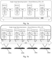
- FIG. 1a shows a system architecture comprising four exits from the node controllers, indicated as FNC in the figure, to an on-chip distributed switching 200.
- Each node comprises at least one CPU where the at least one CPU includes one or more local caches.
- the node controllers according to the first embodiment is not associated with node controller caches. Whether to include such caches or not is a trade-off, where among others designers have to take into consideration the character of the data traffic. Caches associated with the FPGA-controllers is of little use and will reduce the overall performance if the data traffic pattern does not have a "repeatable" character, i.e. if data in the cache is not reused.
- the character of the traffic is dependent of the tasks to be carried out.
- Data base inquiries can be random and reuse of data is not likely to happen, hence a local cache is not of any use, in contrast software programs running repeatable routines might reuse data and hence a local cache associated with an FPGA-node controller can be favourable.
- the second embodiment of an FPGA-controller includes local caches associated with the FPGA's.
- the at least one CPU of each node is also connected to an FPGA node controller.
- the node controller of a first node is interconnected with a second, a third and a fourth node.
- the interconnection can be carried out using different types of fabric connections 200 such as cross bar switches or any other suitable switch.
- the interconnection 200 can be through Ethernet, Omnipath or Infiniband switches.
- the switching fabric can be 1D, 2D and 3D (Torus) this is not shown in the drawings and it will be explained below with reference to another figure.
- the node controllers provide cache coherency and memory coherency within the system in figure 1a . Obviously, the system shown in figure 1a can be extended both with respect of the number of nodes and with respect to the components within each single node.
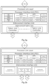
- FIG. 2a shows a block diagram of an FPGA-node controller.
- the node controller is provided with interfaces for communication with CPU's, memories, other node controllers etc.
- bidirectional Coherent Interface is shown at the top of the figure one CIF.
- the CIF connects the node controller with one or more CPU's within the same node.
- the at least one CIF communicates with the FPGA-node controller through an on-chip "Processor Link Layer".
- the routing layer is CPU-specific, and can be changed in the FPGA since the FPGA is fully programmable. Each CPU type will require a specific PHY layer since the CIF is proprietary to each CPU vendor.
- the routing layer can also be programmed to tunnel transactions between two CIFs in the case of dual or multiple CIF connections to the FPGA.
- a processor Interface Unit is also embedded in the FPGA-node controller, the processor interface Unit translates the transactions specific to the particular CPU architecture into a global cache coherence protocol and transfers the transactions to cache coherence protocol engines. Communication with remote and local memories and caches requires that the requester, the FPGA-node controller in question, speaks the same language as the receivers. Hence both a local Memory Protocol Engine LMPE and a Remote Memory Protocol Engine, RMPE, is included in the FPGA-node controller. The LMPE and RMPE sets up the correct protocols to match data transfer between memories within a node as well as between nodes. Apart from the Processor Link Layer the FPGA-node controller can be configured for different CPUs by flash memory programming.
- the node controller includes on-chip fabrics shown as an "Interconnect Fabric Unit".
- the Interconnect Fabric Unit links the node controller to other nodes in a system of nodes.
- the interface between the node controller and remote nodes is shown as two HSSI-gates.
- the on-chip switch routes traffic from the node controller to the fabric link controllers and further to the HSSI-gates.
- the width of the interconnect fabric ports can be flexibly configured to accommodate a number of ports that is the multiple of the number of lanes per port and the number of ports. I.e. if there are 16 lanes available for the fabric ports, these can be configured as 16 separate ports, 4 times 4-lane ports, two 8-lane ports, etc.
- LMTag Three boxes are indicated next to the LMPE, namely LMTag, RMTag and NCache. All of them are optional, and any one of them can me omitted. Moreover it is not mandatory to include all of, or any of, the elements BTE, APIC and TIMER. In Figure 2a, 2b and 2c this is indicated by showing the "boxes" with dotted lines.
- An on-chip NCache acting as a "victim" cache can be efficient for many workloads even if it is very small.
- An on-chip NCache does not have the same drawback as an off-chip cache with regards to bandwidth and latency considerations.
- a separate drawing which excludes the NCache has not been provided for illustration of the first embodiment of the FPGA-node controller. The NCache will be described further with respect to the FPGA-node controller.
- LMPE is the Local Memory Protocol Engine.
- the LMPE is an engine specifically designed to handle memory transactions through executing microcode firmware.
- the firmware is specific to the particular processor architecture's cache coherence protocol. It handles all memory transactions that are directed from an external processor to the memory connected to the processors local to the Node Controller.
- RMPE is the Remote Memory Protocol Engine. The RMPE handles the memory transactions that are destined to operate on memory connected with processors that are located on the other side of the Coherent Interface Fabric.
- the RMPE is also controlled by microcode firmware and programmed to be compliant with the cache coherence protocol of the particular processor architecture.
- MCMS is the Multi Context Micro Sequencer and can be present as a number of separate instances depending on the amount of outstanding memory transactions that is necessary to satisfy the performance requirements for a particular implementation.
- the MCMS handles the sequencing of the microinstructions in the microcode firmware.
- LMTag is the Local Memory directory tag.
- the LMTag encodes the state of the memory lines of the processors local to the Node Controller. The memory lines are equal in size to the granularity for the particular processor architecture. Most modern processor architectures use 64 bytes as the granularity of the objects that are contained in the processor cache memories.
- RMTag is the Remote Memory directory Tag.
- Figure 2b shows a block diagram of an FPGA-node controller.
- the block diagram resembles that of fig. 2a except for the addition of Accelerator Functional Unit -1 and the Accelerator Functional Unit-2.
- the figure 2b indicates two additional Accelerator Functional Units, however it is a matter of design and one, two or more Accelerator Functional Units can be added.
- the Accelerator Functional Units can be used to relieve the CPU from tasks and/or to carry out tasks such as inspection of data, search for particular bit patterns and carry out special functions.
- the functions can be tailored according to wish as they are programmable.
- the Accelerator Functional Units can be arranged so that all data routed through the Fabric Link Controllers with a HSSI-protocol are routed through the Accelerator Functional Units or the Accelerator Functional Units can sniff data to and from the Fabric Link Controllers.
- the Accelerator Functional Units can also be activated by control register signalling, hence activated based on need. Feedback from the Accelerator Functional Units to an associated CPU can be an interrupt to the CPU hence keeping the CPU undisturbed until request is received at the CPU.
- Figure 1b shows a system architecture comprising four devices 100a, 100b, 100c, 100d, each device being a computer, a server or a blade server - above referred to as a node 100a, 100b, 100c, 100d.
- Each node 100a, 100b, 100c, 100d comprises at least one CPU where the at least one CPU includes or are associated with one or more local caches.
- the local caches are further connected to the local CPU memory.
- the at least one CPU of each node is also connected to a Node controller.
- Each node controller is provided with or associated with its own node controller cache.
- the node controller of a first node 100a is interconnected with the node controllers of a second 100b, a third 100c and a fourth 100d node.
- the interconnection can be carried out using different types of fabric connections 200 such as cross bar switches or any other suitable switch. In some aspects of the invention the interconnection 200 can be switching over Ethernet, Omnipath or Infiniband.
- the switching fabric can be 1D, 2D and 3D (Torus) this is not shown in the drawings and it will be explained below with reference to another figure.
- the node controllers provide cache coherency and memory coherency within the system in figure 1b . Obviously, the system shown in figure 1b can be extended both with respect of the number of nodes and with respect to the components within each single node 100a, 100b, 100c, 100d.
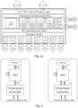
- FIG. 2c shows a block diagram of an FPGA-node controller.
- the node controller is provided with interfaces for communication with CPU's, memories, other node controllers etc.
- bidirectional Coherent Interfaces are shown.
- the CIF connects the node controller with one or more CPU's within the same node.
- the at least one CIF communicates with the FPGA-node controller through an on-chip "Coherent Interface "PHY" Link & Routing Layer".
- a processor Interface Unit is also embedded in the FPGA-node controller, the processor interface Unit translates the transactions specific to the particular CPU architecture into a global cache coherence protocol and transfers the transactions to cache coherence protocol engines.
- the FPGA-node controller in question, speaks the same language as the receivers.
- a local Memory Protocol Engine LMPE and a Remote Memory Protocol Engine, RMPE is included in the FPGA-node controller.
- the LMPE and RMPE sets up the correct protocols to match data transfer between memories within a node as well as between nodes.
- the FPGA-node controller can be configured for different CPUs by firmware downloading.
- the node controller includes on-chip fabrics shown as a crossbar switch. The crossbar switch links the node controller to other nodes in a system of nodes.
- the interface between the node controller and remote nodes is shown as eight Coherent Fabric Links (CFL) gates.
- CFL Coherent Fabric Links
- the on-chip crossbar switch routes traffic from the node controller to the correct CFL gate and further to the correct memory/cache.
- Link controllers, LC are provided in between the CFL gates and the crossbar switch.
- DRAM IF is shown as two bidirectional links on the right side of the block diagram of figure 2c .
- DRAM IF provides interface between the FPGA-node controller and its associated node controller directory tag and/or cache.
- three boxes are indicated next to the DRAM IF gates, namely LMTag, RMTag and NCache.
- the NCache is an on-chip cache for caching remote data to be used by local processors. This cache keeps the most recently used data residing in the off-chip cache located in one of the external DRAM modules.
- the NCache in figure 2c corresponds with the Node Controller Cache shown in figure 1b .
- the FPGA-node controller further includes an I/O Agent visualised as a box to the left in figure 2c .
- the I/O agent handles input and output of non-coherent memory transactions issued by the processors and other housekeeping tasks for accessing control registers and status registers that can be operated upon by the operating system or a separate system maintenance processor.
- the status registers keep information from error counters and error correcting circuits that are included to provide data consistency in case of soft errors in data-paths, interconnect fabric links and processor links.
- the LMPE is the Local Memory Protocol Engine.
- the LMPE is a programmable engine specifically designed to handle memory transactions through executing microcode firmware.
- the firmware is specific to the particular processor architecture's cache coherence protocol. It handles all memory transactions that are directed from an external processor to the memory connected to the processors local to the Node Controller.
- RMPE is the Remote Memory Protocol Engine.
- the RMPE handles the memory transactions that are destined to operate on memory connected with processors that are located on the other side of the Coherent Interface Fabric.
- the RMPE is also controlled by microcode firmware and programmed to be compliant with the cache coherence protocol of the particular processor architecture.
- MCMS is the Multi Context Micro Sequencer and can be present as a number of separate instances depending on the amount of outstanding memory transactions that is necessary to satisfy the performance requirements for a particular implementation.
- the MCMS handles the sequencing of the microinstructions in the microcode firmware.
- LMTag is the Local Memory directory tag.
- the LMTag encodes the state of the memory lines of the processors local to the Node Controller. The memory lines are equal in size to the granularity for the particular processor architecture. Most modern processor architectures use 64 bytes as the granularity of the objects that are contained in the processor cache memories.
- RMTag is the Remote Memory directory Tag
- the RMTag encodes the state of the cache lines contained in the NCache and also contains pointers is some form to identify the address of the Node Controller on the remote node where the corresponding memory addresses are located.
- NCache is the NumaCache. The NCache holds the most recently used memory lines from the processors associated with the remote Node Controllers.
- the FPGA-node-controller with two different node options are shown in figure 3 and figure 4 , the first option in figure 3 and the second in figure 4 .
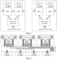
- Figure 3 shows two simplified nodes each node includes at least one CPU, one FPGA-node-controller, and one Memory associated with the CPU. Details are not included and the FPGA-node-controller can in accordance with the second embodiment include its own cachememory. From the FPGA-node-controller it is shown eight Coherent Fabric Links (CFL). These coherent fabric links corresponds with the CFL described with reference to figure 2c .
- CFL Coherent Fabric Links
- the interface between the FPGA-node-controller and the CPU is shown as one coherent interface, CIF, on the left side and two coherent interfaces on the right node in figure 3 .
- Peripheral Interconnect Express, PCle is shown as the interface between the CPU's and components outside of the node. Other bus standards for connecting peripherals might be used.
- a dedicated memory interface is provided between the CPU and the local memory within the node.
- the difference between the right hand side node and the left hand side node of figure 3 is as mentioned that the right hand side is provided with two coherent interfaces between the CPU and the FPGA-node-controller.
- Figure 4 shows the second node option the second option is a scaledup version of the first option, as this second option shows nodes with two CPU's each.
- This is shown as an example as the system according to the present invention scales well and the number of CPU's can far exceed two. It can be seen that a single FPGA-node controller handles two CPU's over a bidirectional coherent interface link. The same applies between the two CPU's, whilst the interface between the individual CPU's associated memory is provided as two bidirectional memory interfaces.
- the interface between the CPU's and external components is exemplified as Peripheral Component Interconnect-express as was also the case in figure 3 .
- Figure 5 shows an example of three nodes in a system, in this example each node is provided with two CPU's which correspond to the configuration shown in figure 4 .
- Each node is connected directly to 7 other nodes through printed circuit board backplanes or cables, hence the FPGA-node-controller in one node can communicate over a coherent fabric link, CFL, with a FPGA-node-controller in any neighbouring node of the system.
- the system example of figure 5 indicates a system, which can include 8 blades plus expansion ports to connect to same expansion ports in other crates to expand the system size. The eight blades correspond with seven coherent fabric links indicated for each FPGA-node-controller.
- Each FPGA-node-controller within each node is connected with two CPU's over a coherent interface. It can be seen that the CPUs are interconnected over a coherent interface; also, the CPU's are connected with peripherals over PCle as was also the case in figure 3 and 4 .
- Fig. 6 shows a single chassis system comprising eight nodes fully interconnected in a one-hop configuration. As can be seen all nodes can access each other without any intermediate hops. The nodes are visualised as circles which are interconnected with "solid" lines.
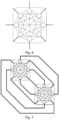
- Figure 7 shows a dual chassis system comprising 16 nodes in a Dragonfly topology with redundant paths. This topology doubles the capacity of the single chassis system in figure 6 at the price of introducing one intermediate hop for some connections between nodes.
- Figure 8 shows a quad chassis system comprising 32 nodes in a Dragonfly topology with redundant paths.
- This topology doubles the capacity i.e. the number of nodes compared with the dual chassis blade system.
- the prize to pay for doubling the capacity is that a maximum of two intermediate hops are introduced, obviously introducing more hops introduces delays in the system Still the topology is a good trade-off between capacity and delays.
- FIG 9 it is disclosed an eight chassis system comprising 64 nodes in a Dragonfly topology with redundant paths.
- the table routed on-chip crossbar used in the present description allows for a multitude of different topologies in addition to the previously described direct connected and dragonfly topologies without the use of external switching.
- the most relevant additional topologies to use are 1D, 2D and 3D Torus topologies.
- a one dimensional system means that nodes are interconnected along one single path (ring), whilst two dimensional switching means that nodes can be interconnected in a matrix. Travelling path from nodes at the top of the matrix to the bottom of the matrix then involves several hops. If this matrix is "folded together" such that the "lowermost” nodes becomes the neighbours of the "uppermost” nodes the number of hops is reduced, in fact in the described situation no hop will be necessary.
- This configuration can be visualised as a "tube”. This solution however does not solve the problems regarding paths in the direction normal to the path from "upper to lower” nodes. By bending the "tube” into a “donut” the number of hops in all directions will statistically be fewer.
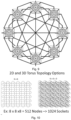
- Figure 10 shows schematic examples of a matrix topology with 6 x 6 nodes to the left.
- the topology resembles a "double folded matrix" as the bottom and top nodes are interconnected this alone resembles the tube example above, additionally the left most nodes are connected with the right most nodes making a "double folded matrix or a donut.
- the figure to the right shows a 3D expanded version of the left matrix, with three layers interconnected resulting in a 6 x 6 x 3 network.
- Such a 3D topology scales well and an 8 x 8 x 8 network topology is indicated by text at the bottom of figure 16, such a topology would result in 512 nodes and altogether 1024 CPU sockets with 2 CPU sockets per node.
- a computer such as but not limited to. Ethernet switch, Omnipath switch and Infiniband switch, CFL Coherent Fabric Link CIF Coherent Interface CSR Control Space Registers FPGA Field Programmable Gate Array FNC Field Programmable Gate Array Node Controller HT Hyper Transport HSSI High Speed Serial Interface.
Landscapes
- Engineering & Computer Science (AREA)
- Theoretical Computer Science (AREA)
- Physics & Mathematics (AREA)
- General Engineering & Computer Science (AREA)
- Computer Hardware Design (AREA)
- General Physics & Mathematics (AREA)
- Mathematical Physics (AREA)
- Software Systems (AREA)
- Computing Systems (AREA)
- Memory System Of A Hierarchy Structure (AREA)
- Multi Processors (AREA)
Description
- The present invention relates to a multiprocessor memory sharing systems including node controllers. In a scalable shared memory system with multiple general purpose central processing units the present invention uses transaction engines to perform actions required to maintain system wide cache and memory coherency.
- The introduction of Field Programmable Gate Arrays (FPGAs) has opened opportunities to use such circuits in a plurality of ways as components in computing systems. The present invention combines the FPGA capabilities with a specific type of functionality. The functionality can be described as a Node Controller in a scalable computer system with multiple central processing units (CPUs) where all the processors can share and operate on all the available memory and where all the caches and the corresponding memory locations in the system are kept coherent with respect to the valid data produced by the processors.
- Modern processors have capabilities of interconnecting a relatively low number of processor modules to form larger systems by direct connections between the processors across point-to-point links. Each processor module contains a number of CPU cores. These links are not capable of expanding the system size beyond typically 4-8 modules, although some may go as far as a maximum of 16. For performance reasons, the directly connected systems are limited to 8 modules due to the increasing inefficiency in the protocols that handle the housekeeping task to maintain data coherency across all memories and high speed caches in the system.
- By cache coherence, it is meant consistency of shared data stored in multiple local caches. In a multi-processor system with multiple local caches, data that reside in these caches must be updated or invalidated such that accesses to the data will reflect the latest values stored by any given processor with access to that data. Processors operate independently of each other and thereby influence on the caches independently of each other and without cache coherence logic, shared data would not be valid and would cause inconsistent results for multithreaded programs that use the data.
- Cache coherence is intended to manage and maintain consistency between the caches and memory.
- Multiprocessor memory sharing systems has normally been carried out with hard-wired application specific integrated circuits (ASICs) using state machines that cannot be changed after the ASIC has been manufactured. This requires a very comprehensive verification program to be conducted before the ASIC is produced and leaves no room for correcting any potential errors in the state machines without making a new ASIC. This is both expensive and time consuming.
-
US 7,406,086 B2 discloses a method and apparatus for parallel processing. One embodiment provides a multiprocessor computer system that includes a first and second node controller, a number of processors being connected to each node controllers, a memory connected to each controller, a first input/output system connected to the first node controller, and a communications network connected between the node controllers. -
United states patent 6,115,804 discloses a non uniform memory access computer system which includes first and second processing nodes that are each coupled to a node interconnect. - The patent application
JP P2016-63350A - The patent publication
US 6,094,686 relates to multi-processor system for transferring data without incurring deadlock using hierarchical virtual channels. It is discussed an architecture and coherency protocol for use in large SMP computer system includes a hierarchical switch structure which allows for a number of multi-processor nodes to be coupled to the switch to operate at an optimum performance. - The patent publication
WO 2016/144953 A1 relates to an apparatus and methods for monitoring errors during idle times in high-speed links including a physical Coding Sublayer (PCS), however it does not discuss coherency in multiprocessor systems sharing memories. - U.S. patent
US 7,315,919 B1 relates to snooping based cache coherence system to maintain consistency among cache memories of multiprocessing nodes. -
US 2016/0147658 A1 describes Topology of clusters of processors of a computer configuration, configured to support any of a plurality of cache coherency protocols, is discovered at initialization time to determine which one of the plurality of cache coherency protocols is to be used to handle coherency requests of the configuration. - The patent application
US 2014/0052923 A1 describes a processor which includes a plurality of nodes arranged two dimensionally in the X-axis direction and in the Y-axis direction, and each of the nodes includes a processor core and a distributed shared cache memory. The cache memories included in the respective nodes are divided into banks in the Y-axis direction. Coherency of the cache memories in the X-axis direction is controlled by a snoop system. The cache memories are shared by the nodes. - The patent application
US 2010/0271071 A1 discloses an inter-layer interconnect for multi-layer semiconductor stacks, Each circuit layer in the multi-layer semiconductor stack is required to include an inter-layer interface region that is disposed at substantially the same topographic location such that when the semiconductor dies upon which such circuit layers arc disposed arc arranged together in a stack, electrical conductors disposed within each semiconductor die are aligned with one another to provide an inter-layer bus that is oriented vertically, or transversely, with respect to the individual circuit layers. - According to
US 7 346 744 B1 it is provided methods and an apparatus for increasing the efficiency of data access in a multiple processor, multiple cluster system. Mechanisms for improving the accuracy of information available to a cache coherence controller are provided in order to allow the cache coherence controller to reduce the number of transactions in a multiple cluster system. Non-change probes and augmented non-change probe responses are provided to acquire state information in remote clusters without affecting the state of the probed memory line. Augmented probe responses associated with shared and invalidating probes are provided to update state information in a coherence directory during read and read/write probe requests. - The publication titled" Hardware Fault Containment in Scalable Shared-Memory Multiprocessors" by Dan Teodosiu et al. (doi:10.1007/10704208) shows that fault containment techniques can be effectively applied to scalable shared-memory multiprocessors to reduce the reliability problems created by increased machine size. The primary goal of the authors is to leave normal-mode performance unaffected. Rather than using expensive fault tolerance techniques to mask the effects of data and resource loss, the disclosed strategy is based on limiting the damage caused by faults to only a portion of the machine. After a hardware fault, we run a distributed recovery algorithm that allows normal operation lo be resumed in the functioning parts of the machine.
- The paper titled "Technology-Driven, Highly-Scalable Dragonfly Topology" by John Kim et al. (doi:10.1109/ISCA.2008.19) relates to dragonfly topology which uses a group of routers as a virtual router to increase the effective radix of the network, and hence reduce network diameter, cost, and latency.
- The paper by Nowatzyk A et al: "The S3.Mp Scalable Shared Memory Multiprocessor", (doi:10.1109/HICSS.1994.323149) discloses Sun's Scalable Shared memory MultiProcessor project.
- This is a research project to demonstrate a low overhead, high throughput communication system that is based on cache coherent distributed shared memory (DSM). S3.mp uses distributed directories and point-to-point messages that are sent over a packet switched interconnect fabric to achieve scalability over a wide range of configurations. S3.mp uses a new CMOS serial link technology that achieves transmission rates above 1 Gbit/sec and that is directly integrated into a packet router chip. Unlike other DSM systems, S3.mp can·be spatially distributed over a local area via fibre optic links. This capability allows S3.mp to interconnect clusters of workstations to form multiprocessor workgroups that efficiently share memory, processors and 1/0 devices. Multichip module technology, the integrated arbitrary topology router, fast serial links, and a cache coherent DSM system that is integrated into the memory controller allow compact, massively parallel S3.mp systems.
- The paper by Tom Lovett et al: "Sting: A CC-NUMA Computer System for the Commercial Marketplace", (doi:10.1145/232973.233006) discloses a Cache Coherent Non-Uniform Memory Access (CC-NUMA) Multiprocessor designed and built by Sequent Computer Systems, Inc. It combines four processor Symmetric Multiprocessor (SMP) nodes (called Quads), using a Scalable Coherent Interface (SCI) based coherent interconnect. The Quads are based on the Intel P6 processor and the external bus it defines. In addition to 4 P6 processors, each Quad may contain up to 4 GBytes of system memory, 2 Peripheral Component Interface (PC/) busses for I/0, and a Lynx board. The Lynx board provides the data path to the SCI-based interconnect and ensures systemwide cache coherency. STiNG is one of the first commercial CCNUMA systems to be built. This paper describes the motivation for building STiNG as well as its architecture and implementation. In addition, performance analysis is provided for On-Line Transaction Processing (OLTP) and Decision Support System (DSS) workloads. Finally, the status of the current implementation is reviewed.
- The paper by Hermann Hellwagner: "The SCI Standard and Applications of SCI", (ISBN:978-3-540-66696-7) provides an overview of the Scalable Coherent Interface (SCI), an ANSI/IEEE standard for high-speed interconnects in computing and networking. It focuses on SCI's application as a network for compute clusters, while acknowledging its broader uses and implementations. The chapter introduces SCI's basic concepts and standards, discusses its principal objectives and features, and outlines its applications in various domains such as system area networks, memory interconnects for multiprocessors, I/O subsystems, and data acquisition systems. The paper aims to provide foundational knowledge of SCI and its versatility, with technical details available in the referenced literature.
- The paper by Kuskin J Et AI: "The Stanford FLASH multiprocessor", (doi:10.1109/ISCA.1994.288140) discloses that the FLASH multiprocessor efficiently integrates support for cache-coherent shared memory and highperformance message passing, while minimizing both hardware and software overhead. Each node in FLASH contains a microprocessor, a portion of the machine's global memory, a port to the interconnection network, an I/O interface, and a custom node controller called MAGIC. Toe MAGIC chip handles all communication both within the node and among nodes, using hardwired data paths for efficient data movement and a programmable processor optimized for executing protocol operations. The use of the protocol processor makes FLASH very flexible - it can support a variety of different communication mechanisms - and simplifies the design and implementation. This paper presents the architecture of FLASH and MAG~C. and discusses the base cache-coherence and message-passing protocols. Latency and occupancy numbers, which are derived from our system-level simulator and our Verilog code, are given for several common protocol operations. The paper also describes our software strategy and FLASH's current status.
- It is one object of the invention to provide a flexible Node Controller for multiple processor systems with memory sharing, which do not suffer from the problems indicated above, in particular the problems related to the tedious verification and testing necessary for node controllers in multi-processor systems.
- The present invention is defined in the appended independent claims to which reference should be made. Advantageous features are set out in the appended dependent claims.
- Following is a brief description of the drawings in order to make the invention more readily understandable, the discussion that follows will refer to the accompanying drawings, in which
-
Fig. 1a shows an example of system architecture without node controller caches, -
Fig. 1b shows an example of system architecture with node controller caches, -
Fig. 2a shows a block diagram of an FPGA node controller comprising a cache memory, -
Fig. 2b shows another block diagram of an FPGA node controller comprising a cache memory, -
Fig. 2c shows another block diagram of an FPGA node controller, -
Fig. 3 shows two first examples of FPGA Node Controllers in communication with CPUs and coherent fabric links, -
Fig. 4 shows two second examples of FPGA Node Controllers in communication with CPUs and coherent fabric links, -
Fig. 5 shows a system example including Node Controllers, CPU's and I/O peripherals, -
Fig. 6 shows a single chassis blade system comprising eight nodes fully interconnected in a one-hop configuration, -
Fig. 7 shows a dual chassis blade system comprising 16 nodes in a Dragonfly topology with redundant paths, -
Fig. 8 shows a quad chassis blade system comprising 32 nodes in a Dragonfly topology with redundant paths, -
Fig. 9 shows an eight chassis blade system comprising 64 nodes in a Dragonfly topology with redundant paths, -
Fig. 10 shows a 2D Torus topology on the left hand and a 3D Torus topology on the right hand side. - In the following it is firstly disclosed general embodiments in accordance with the present invention, thereafter particular exemplary embodiments will be described. Where possible reference will be made to the accompanying drawings and where possible using reference numerals in the drawings. In the description below it is described how to combine FPGA capabilities with a specific type of functionality. The functionality can be described as a Node Controller in a scalable computer system with multiple central processing units (CPUs) where all the processors can share and operate on all the available memory and where all the caches and the corresponding memory locations in the system are kept coherent with respect to the valid data produced by the processors.
- The invention is based on using an FPGA in close proximity to a CPU with respect to connectivity. The FPGA is connected to the interprocessor communication link of a processor such as the HyperTransport™ for AMD, QPI™ and UPI™ from Intel, CCPI™ from Cavium, NVLink™ from Nvidia or CAPI™ from IBM. Through this type of connection, the FPGA Node Controller (FNC) will act as an interface for multiple CPU modules to be connected to form scalable multiprocessor systems.
- In one example a Node Controller (NC) is connected to a server processor's coherent interface. The Node Controller manages information packets generated by CPUs and transferred by the coherent interface to the Node Controller to perform memory transactions in the form of read/write operations and other special transactions that are used to send management signals between the different memory and cache units in a computer system in order to keep the data contained in the memory and cache units coherent, i.e. any given entity in the memory system should reflect the latest update done by any processor in the system. Multiple such Node Controllers can be connected to each other across an interconnect fabric and set up to form a unified shared memory computer system.
- Modern CPUs are equipped with coherent links to connect a small number, of CPUs into a larger shared memory system - a "Node". Larger systems will have to be built using special circuitry to connect "Nodes" together to form a larger shared memory system consisting of a number of such Nodes. A Node can typically contain from 1 to 4 CPUs and one or more Node Controllers.
- According to the present invention the Node Controller is a FPGA Node controller. The programmability enables correcting initial design errors in addition to allow for field upgrades and optimizations done at a later stage. FPGA-programming can be executed by the use of programmable flash memories. The flash-memories might be accessed by traditional input devices such as from computers. It also reduces the risk of not having a workable product with the first version of the Node Controller since design flaws can be corrected.
- The present invention will now be described in detail with support from the drawings.
-
Figure 1a shows a system architecture comprising four exits from the node controllers, indicated as FNC in the figure, to an on-chip distributed switching 200. Each node comprises at least one CPU where the at least one CPU includes one or more local caches. In the second embodiment of the FPGA-node controller the node controllers according to the first embodiment is not associated with node controller caches. Whether to include such caches or not is a trade-off, where among others designers have to take into consideration the character of the data traffic. Caches associated with the FPGA-controllers is of little use and will reduce the overall performance if the data traffic pattern does not have a "repeatable" character, i.e. if data in the cache is not reused. In such situations including caches in the system only causes extra traffic. The character of the traffic is dependent of the tasks to be carried out. Data base inquiries can be random and reuse of data is not likely to happen, hence a local cache is not of any use, in contrast software programs running repeatable routines might reuse data and hence a local cache associated with an FPGA-node controller can be favourable. The second embodiment of an FPGA-controller includes local caches associated with the FPGA's. - The at least one CPU of each node is also connected to an FPGA node controller. The node controller of a first node is interconnected with a second, a third and a fourth node. The interconnection can be carried out using different types of
fabric connections 200 such as cross bar switches or any other suitable switch. In some aspects of the invention theinterconnection 200 can be through Ethernet, Omnipath or Infiniband switches. - The switching fabric can be 1D, 2D and 3D (Torus) this is not shown in the drawings and it will be explained below with reference to another figure. The node controllers provide cache coherency and memory coherency within the system in
figure 1a . Obviously, the system shown infigure 1a can be extended both with respect of the number of nodes and with respect to the components within each single node. -
Figure 2a shows a block diagram of an FPGA-node controller. The node controller is provided with interfaces for communication with CPU's, memories, other node controllers etc. At the top of the figure one CIF, bidirectional Coherent Interface is shown. The CIF connects the node controller with one or more CPU's within the same node. The at least one CIF communicates with the FPGA-node controller through an on-chip "Processor Link Layer". The routing layer is CPU-specific, and can be changed in the FPGA since the FPGA is fully programmable. Each CPU type will require a specific PHY layer since the CIF is proprietary to each CPU vendor. The routing layer can also be programmed to tunnel transactions between two CIFs in the case of dual or multiple CIF connections to the FPGA. A processor Interface Unit is also embedded in the FPGA-node controller, the processor interface Unit translates the transactions specific to the particular CPU architecture into a global cache coherence protocol and transfers the transactions to cache coherence protocol engines. Communication with remote and local memories and caches requires that the requester, the FPGA-node controller in question, speaks the same language as the receivers. Hence both a local Memory Protocol Engine LMPE and a Remote Memory Protocol Engine, RMPE, is included in the FPGA-node controller. The LMPE and RMPE sets up the correct protocols to match data transfer between memories within a node as well as between nodes. Apart from the Processor Link Layer the FPGA-node controller can be configured for different CPUs by flash memory programming. The node controller includes on-chip fabrics shown as an "Interconnect Fabric Unit". The Interconnect Fabric Unit links the node controller to other nodes in a system of nodes. The interface between the node controller and remote nodes is shown as two HSSI-gates. The on-chip switch routes traffic from the node controller to the fabric link controllers and further to the HSSI-gates. - The width of the interconnect fabric ports can be flexibly configured to accommodate a number of ports that is the multiple of the number of lanes per port and the number of ports. I.e. if there are 16 lanes available for the fabric ports, these can be configured as 16 separate ports, 4 times 4-lane ports, two 8-lane ports, etc.
- Three boxes are indicated next to the LMPE, namely LMTag, RMTag and NCache. All of them are optional, and any one of them can me omitted. Moreover it is not mandatory to include all of, or any of, the elements BTE, APIC and TIMER. In
Figure 2a, 2b and2c this is indicated by showing the "boxes" with dotted lines. An on-chip NCache acting as a "victim" cache can be efficient for many workloads even if it is very small. An on-chip NCache does not have the same drawback as an off-chip cache with regards to bandwidth and latency considerations. A separate drawing which excludes the NCache has not been provided for illustration of the first embodiment of the FPGA-node controller. The NCache will be described further with respect to the FPGA-node controller. - LMPE is the Local Memory Protocol Engine. The LMPE is an engine specifically designed to handle memory transactions through executing microcode firmware. The firmware is specific to the particular processor architecture's cache coherence protocol. It handles all memory transactions that are directed from an external processor to the memory connected to the processors local to the Node Controller. RMPE is the Remote Memory Protocol Engine. The RMPE handles the memory transactions that are destined to operate on memory connected with processors that are located on the other side of the Coherent Interface Fabric. The RMPE is also controlled by microcode firmware and programmed to be compliant with the cache coherence protocol of the particular processor architecture.
- MCMS is the Multi Context Micro Sequencer and can be present as a number of separate instances depending on the amount of outstanding memory transactions that is necessary to satisfy the performance requirements for a particular implementation. The MCMS handles the sequencing of the microinstructions in the microcode firmware. LMTag is the Local Memory directory tag. The LMTag encodes the state of the memory lines of the processors local to the Node Controller. The memory lines are equal in size to the granularity for the particular processor architecture. Most modern processor architectures use 64 bytes as the granularity of the objects that are contained in the processor cache memories.
- RMTag is the Remote Memory directory Tag.
-
Figure 2b shows a block diagram of an FPGA-node controller. The block diagram resembles that offig. 2a except for the addition of Accelerator Functional Unit -1 and the Accelerator Functional Unit-2. Thefigure 2b indicates two additional Accelerator Functional Units, however it is a matter of design and one, two or more Accelerator Functional Units can be added. The Accelerator Functional Units can be used to relieve the CPU from tasks and/or to carry out tasks such as inspection of data, search for particular bit patterns and carry out special functions. The functions can be tailored according to wish as they are programmable. The Accelerator Functional Units can be arranged so that all data routed through the Fabric Link Controllers with a HSSI-protocol are routed through the Accelerator Functional Units or the Accelerator Functional Units can sniff data to and from the Fabric Link Controllers. The Accelerator Functional Units can also be activated by control register signalling, hence activated based on need. Feedback from the Accelerator Functional Units to an associated CPU can be an interrupt to the CPU hence keeping the CPU undisturbed until request is received at the CPU. -
Figure 1b shows a system architecture comprising fourdevices node node first node 100a is interconnected with the node controllers of a second 100b, a third 100c and a fourth 100d node. The interconnection can be carried out using different types offabric connections 200 such as cross bar switches or any other suitable switch. In some aspects of the invention theinterconnection 200 can be switching over Ethernet, Omnipath or Infiniband. - The switching fabric can be 1D, 2D and 3D (Torus) this is not shown in the drawings and it will be explained below with reference to another figure. The node controllers provide cache coherency and memory coherency within the system in
figure 1b . Obviously, the system shown infigure 1b can be extended both with respect of the number of nodes and with respect to the components within eachsingle node -
Figure 2c shows a block diagram of an FPGA-node controller. The node controller is provided with interfaces for communication with CPU's, memories, other node controllers etc. At the top of the figure two CIF, bidirectional Coherent Interfaces are shown. The CIF connects the node controller with one or more CPU's within the same node. The at least one CIF communicates with the FPGA-node controller through an on-chip "Coherent Interface "PHY" Link & Routing Layer". A processor Interface Unit is also embedded in the FPGA-node controller, the processor interface Unit translates the transactions specific to the particular CPU architecture into a global cache coherence protocol and transfers the transactions to cache coherence protocol engines. Communication with remote and local memories and caches requires that the requester, the FPGA-node controller in question, speaks the same language as the receivers. Hence both a local Memory Protocol Engine LMPE and a Remote Memory Protocol Engine, RMPE, is included in the FPGA-node controller. The LMPE and RMPE sets up the correct protocols to match data transfer between memories within a node as well as between nodes. Apart from the Routing layer (Coherent Interface "PHY" Link & Routing Layer) the FPGA-node controller can be configured for different CPUs by firmware downloading. The node controller includes on-chip fabrics shown as a crossbar switch. The crossbar switch links the node controller to other nodes in a system of nodes. The interface between the node controller and remote nodes is shown as eight Coherent Fabric Links (CFL) gates. The on-chip crossbar switch routes traffic from the node controller to the correct CFL gate and further to the correct memory/cache. Link controllers, LC, are provided in between the CFL gates and the crossbar switch. - DRAM IF is shown as two bidirectional links on the right side of the block diagram of
figure 2c . There is one or more DRAM IF providing interface between the FPGA-node controller and its associated node controller directory tag and/or cache. In the case of using the DRAM, three boxes are indicated next to the DRAM IF gates, namely LMTag, RMTag and NCache. The NCache is an on-chip cache for caching remote data to be used by local processors. This cache keeps the most recently used data residing in the off-chip cache located in one of the external DRAM modules. The NCache infigure 2c corresponds with the Node Controller Cache shown infigure 1b . - The FPGA-node controller further includes an I/O Agent visualised as a box to the left in
figure 2c . The I/O agent handles input and output of non-coherent memory transactions issued by the processors and other housekeeping tasks for accessing control registers and status registers that can be operated upon by the operating system or a separate system maintenance processor. The status registers keep information from error counters and error correcting circuits that are included to provide data consistency in case of soft errors in data-paths, interconnect fabric links and processor links. - LMPE is the Local Memory Protocol Engine. The LMPE is a programmable engine specifically designed to handle memory transactions through executing microcode firmware. The firmware is specific to the particular processor architecture's cache coherence protocol. It handles all memory transactions that are directed from an external processor to the memory connected to the processors local to the Node Controller.
- RMPE is the Remote Memory Protocol Engine. The RMPE handles the memory transactions that are destined to operate on memory connected with processors that are located on the other side of the Coherent Interface Fabric. The RMPE is also controlled by microcode firmware and programmed to be compliant with the cache coherence protocol of the particular processor architecture.
- MCMS is the Multi Context Micro Sequencer and can be present as a number of separate instances depending on the amount of outstanding memory transactions that is necessary to satisfy the performance requirements for a particular implementation. The MCMS handles the sequencing of the microinstructions in the microcode firmware. LMTag is the Local Memory directory tag. The LMTag encodes the state of the memory lines of the processors local to the Node Controller. The memory lines are equal in size to the granularity for the particular processor architecture. Most modern processor architectures use 64 bytes as the granularity of the objects that are contained in the processor cache memories.
- RMTag is the Remote Memory directory Tag, The RMTag encodes the state of the cache lines contained in the NCache and also contains pointers is some form to identify the address of the Node Controller on the remote node where the corresponding memory addresses are located.
- NCache is the NumaCache. The NCache holds the most recently used memory lines from the processors associated with the remote Node Controllers.
- The FPGA-node-controller with two different node options are shown in
figure 3 andfigure 4 , the first option infigure 3 and the second infigure 4 .Figure 3 shows two simplified nodes each node includes at least one CPU, one FPGA-node-controller, and one Memory associated with the CPU. Details are not included and the FPGA-node-controller can in accordance with the second embodiment include its own cachememory. From the FPGA-node-controller it is shown eight Coherent Fabric Links (CFL). These coherent fabric links corresponds with the CFL described with reference tofigure 2c . The interface between the FPGA-node-controller and the CPU is shown as one coherent interface, CIF, on the left side and two coherent interfaces on the right node infigure 3 . Peripheral Interconnect Express, PCle, is shown as the interface between the CPU's and components outside of the node. Other bus standards for connecting peripherals might be used. A dedicated memory interface is provided between the CPU and the local memory within the node. The difference between the right hand side node and the left hand side node offigure 3 is as mentioned that the right hand side is provided with two coherent interfaces between the CPU and the FPGA-node-controller. -
Figure 4 shows the second node option the second option is a scaledup version of the first option, as this second option shows nodes with two CPU's each. This is shown as an example as the system according to the present invention scales well and the number of CPU's can far exceed two. It can be seen that a single FPGA-node controller handles two CPU's over a bidirectional coherent interface link. The same applies between the two CPU's, whilst the interface between the individual CPU's associated memory is provided as two bidirectional memory interfaces. As forfigure 4 the interface between the CPU's and external components is exemplified as Peripheral Component Interconnect-express as was also the case infigure 3 . -
Figure 5 shows an example of three nodes in a system, in this example each node is provided with two CPU's which correspond to the configuration shown infigure 4 . Each node is connected directly to 7 other nodes through printed circuit board backplanes or cables, hence the FPGA-node-controller in one node can communicate over a coherent fabric link, CFL, with a FPGA-node-controller in any neighbouring node of the system. The system example offigure 5 indicates a system, which can include 8 blades plus expansion ports to connect to same expansion ports in other crates to expand the system size. The eight blades correspond with seven coherent fabric links indicated for each FPGA-node-controller. Each FPGA-node-controller within each node is connected with two CPU's over a coherent interface. It can be seen that the CPUs are interconnected over a coherent interface; also, the CPU's are connected with peripherals over PCle as was also the case infigure 3 and4 . -
Fig. 6 shows a single chassis system comprising eight nodes fully interconnected in a one-hop configuration. As can be seen all nodes can access each other without any intermediate hops. The nodes are visualised as circles which are interconnected with "solid" lines. -
Figure 7 shows a dual chassis system comprising 16 nodes in a Dragonfly topology with redundant paths. This topology doubles the capacity of the single chassis system infigure 6 at the price of introducing one intermediate hop for some connections between nodes. -
Figure 8 shows a quad chassis system comprising 32 nodes in a Dragonfly topology with redundant paths. This topology doubles the capacity i.e. the number of nodes compared with the dual chassis blade system. The prize to pay for doubling the capacity is that a maximum of two intermediate hops are introduced, obviously introducing more hops introduces delays in the system Still the topology is a good trade-off between capacity and delays. - Finally, in
figure 9 it is disclosed an eight chassis system comprising 64 nodes in a Dragonfly topology with redundant paths. - Dragonfly topologies introduce redundant paths, which is an advantage for reliability and congestion scenarios.
- The table routed on-chip crossbar used in the present description allows for a multitude of different topologies in addition to the previously described direct connected and dragonfly topologies without the use of external switching. The most relevant additional topologies to use are 1D, 2D and 3D Torus topologies. A one dimensional system means that nodes are interconnected along one single path (ring), whilst two dimensional switching means that nodes can be interconnected in a matrix. Travelling path from nodes at the top of the matrix to the bottom of the matrix then involves several hops. If this matrix is "folded together" such that the "lowermost" nodes becomes the neighbours of the "uppermost" nodes the number of hops is reduced, in fact in the described situation no hop will be necessary. This configuration can be visualised as a "tube". This solution however does not solve the problems regarding paths in the direction normal to the path from "upper to lower" nodes. By bending the "tube" into a "donut" the number of hops in all directions will statistically be fewer.
-
Figure 10 shows schematic examples of a matrix topology with 6 x 6 nodes to the left. The topology resembles a "double folded matrix" as the bottom and top nodes are interconnected this alone resembles the tube example above, additionally the left most nodes are connected with the right most nodes making a "double folded matrix or a donut. The figure to the right shows a 3D expanded version of the left matrix, with three layers interconnected resulting in a 6 x 6 x 3 network. Such a 3D topology scales well and an 8 x 8 x 8 network topology is indicated by text at the bottom of figure 16, such a topology would result in 512 nodes and altogether 1024 CPU sockets with 2 CPU sockets per node.100a, 100b, 100c, 100d A computer, a server or a blade server - above referred to as a node 200 On-chip distributed switching, such as but not limited to. Ethernet switch, Omnipath switch and Infiniband switch, CFL Coherent Fabric Link CIF Coherent Interface CSR Control Space Registers FPGA Field Programmable Gate Array FNC Field Programmable Gate Array Node Controller HT Hyper Transport HSSI High Speed Serial Interface. LC Link Controller LM-Tag Local Memory Tag LMPE Local Memory Protocol Engine MCMS Multi Context Micro Sequencer MIF Memory Interface MMIO Memory Mapped IO NC Node Controller NCache NumaCache (Non-uniform memory access Cache) NUMA Non-uniform memory access PCI-e PCI Express (Peripheral Component Interconnect Express RM-Tag Remote Memory Tag RMPE Remote Memory Protocol Engine SCI Scalable Coherent Interface UPI Ultra Path Interconnect
Claims (15)
- A multiprocessor memory sharing system at least comprising:a first node (100a, 100b, 100c, 100d),a second node (100a, 100b, 100c, 100d) andan interconnect switch (200),the first node comprises a first group of CPU's and at least one first FPGA Node Controller, wherein said first group of CPU's is connected to the at least one first FPGA Node Controller wherein the at least one first FPGA Node Controller comprises cache coherence protocol engines and wherein the first FPGA Node Controller is configured to execute transactions directly or through the interconnect switch (200) to at least one second FPGA Node Controller wherein the at least one second FPGA Node Controller comprises cache coherence protocol engines and wherein the at least one second FPGA Node Controller is connected to a second group of CPU's running a single instance of an operating system, wherein the at least one first FPGA Node Controller at least comprises:a) at least one Coherent Interface Fabric, CIF, configured to connect the at least one first FPGA Node Controller to one or more CPU's within the same node (100a, 100b, 100c, 100d), Wherein the at least one CIF communicates with the at least one first FPGA-node controller through an on-chip "Processor Link Layer";b) a CPU interface unit configured to translate transactions specific to a particular CPU architecture of the CPU's local to the at least one first FPGA Node Controller into a global cache coherence protocol and vice versa; wherein the CPU interface unit is configured to transfer the transactions to the cache coherence protocol engines;c) a remote memory protocol engine, RMPE, being an instance of said cache coherence engines, wherein the RMPE is configured to handle memory transactions that are destined to operate on memory connected with CPU's that are located on another side of said at least one Coherent Interface Fabric, wherein the RMPE is controlled by microcode firmware and programmed to be compliant with a cache coherence protocol of the particular CPU architecture;d) a local memory protocol engine, LMPE, being an instance of said cache coherence engines, wherein the LMPE is an engine specifically designed to handle memory transactions through executing microcode firmware and is configured to handle all memory transactions that are directed from an external CPU to the memory connected to the CPU's local to the Node Controller; andwherein, when the at least one first FPGA Node Controller is configured to execute transactions through the interconnect switch, said at least one first FPGA Node Controller further comprises a crossbar switch, configured to link the FPGA Node Controllers to other nodes (100a, 100b, 100c, 100d) in the multiprocessor memory sharing system of nodes.
- A multiprocessor memory sharing system according to claim 1, where at least one of the FPGA Node Controllers further comprises two HSSI-gates as interface between the at least one FPGA Node Controller and remote nodes (100a, 100b, 100c, 100d).
- A multiprocessor memory sharing system according to claim 1 where the at least one first FPGA Node Controller includes at least one Fabric Link Controller,.
- A multiprocessor memory sharing system according to claim 3 where the at least one Fabric Link Controller includes interconnect fabric ports.
- A multiprocessor memory sharing system according to claim 4 where the width of the interconnect fabric ports can be flexibly configured to accommodate a number of ports that is the multiple of a number of lanes per port.
- A multiprocessor memory sharing system according to claim 1 - 5 where the at least one first FPGA Node Controller is connected to at least one of:• one second FPGA Node Controller in a torus topology, and• one second FPGA Node Controller in a Dragonfly topology.
- A multiprocessor memory sharing system according to claim 1 -6 where the FPGA Node Controllers are interconnected through one of:• an Ethernet switch,• an Omnipath™ switch, and• an InfiniBand switch.
- A multiprocessor memory sharing system according to claim 1 - 7 where the at least one first FPGA Node Controller is connected to separate first memory modules, where the first memory modules contain information about the state of memory and cache locations.
- A multiprocessor memory sharing system according to claim 1 - 7 where the at least one first FPGA Node Controller is connected to separate first memory modules on a first side of the first interconnect switch (200) to store cache lines that belong to a second memory in a second node on a second side of the first interconnect switch (200).
- A multiprocessor memory sharing system according to claim 1 - 9 where the FPGA Node Controllers utilizes internal RAM to implement a partial sectored directory with a minimal memory line tag information to speed up necessary tag lookup.
- A multiprocessor memory sharing system according to claim 1-10 where the FPGA Node Controllers contains multiple instances of a protocol transaction processing engines that perform the necessary transactions on directories and tags to maintain the system with cache and memory coherency.
- A multiprocessor memory sharing system according to claim 1-11 where the at least one first FPGA Node Controller is configured to issue speculative cache line requests to a target responder before the state of the cache line is known to the at least one first FPGA Node Controller and where a transaction can be dropped if the cache line is valid at the requester.
- A multiprocessor memory sharing system according to claim 12, where the target responder is a second node on a second side of the first interconnect change.
- A multiprocessor memory sharing system according any of the claims 1 - 3, where the at least one first FPGA Node Controller comprises at least one Accelerator Functional Unit.
- A multiprocessor memory sharing system according to claim 1, where the at least one first FPGA Node Controller includes local caches associated with the at least one first FPGA Node Controller.
Applications Claiming Priority (2)
| Application Number | Priority Date | Filing Date | Title |
|---|---|---|---|
| NO20170719A NO343359B1 (en) | 2017-05-02 | 2017-05-02 | Interconnect switch in multiprocessor systems |
| PCT/NO2018/050115 WO2018203754A1 (en) | 2017-05-02 | 2018-04-30 | Cache coherent node controller for scale-up shared memory systems |
Publications (3)
| Publication Number | Publication Date |
|---|---|
| EP3619614A1 EP3619614A1 (en) | 2020-03-11 |
| EP3619614C0 EP3619614C0 (en) | 2025-06-04 |
| EP3619614B1 true EP3619614B1 (en) | 2025-06-04 |
Family
ID=62563222
Family Applications (1)
| Application Number | Title | Priority Date | Filing Date |
|---|---|---|---|
| EP18730137.9A Active EP3619614B1 (en) | 2017-05-02 | 2018-04-30 | Cache coherent node controller for scale-up shared memory systems |
Country Status (4)
| Country | Link |
|---|---|
| US (1) | US10956329B2 (en) |
| EP (1) | EP3619614B1 (en) |
| NO (1) | NO343359B1 (en) |
| WO (1) | WO2018203754A1 (en) |
Families Citing this family (6)
| Publication number | Priority date | Publication date | Assignee | Title |
|---|---|---|---|---|
| US11238203B2 (en) * | 2017-06-30 | 2022-02-01 | Intel Corporation | Systems and methods for accessing storage-as-memory |
| EP3973406A1 (en) * | 2020-03-26 | 2022-03-30 | Graphcore Limited | Embedding rings on a toroid computer network |
| US11461263B2 (en) | 2020-04-06 | 2022-10-04 | Samsung Electronics Co., Ltd. | Disaggregated memory server |
| US11714755B2 (en) * | 2020-07-31 | 2023-08-01 | Hewlett Packard Enterprise Development Lp | System and method for scalable hardware-coherent memory nodes |
| US11573898B2 (en) | 2020-08-17 | 2023-02-07 | Hewlett Packard Enterprise Development Lp | System and method for facilitating hybrid hardware-managed and software-managed cache coherency for distributed computing |
| CN112416850A (en) * | 2020-11-20 | 2021-02-26 | 新华三云计算技术有限公司 | A multi-processor interconnected system and its communication method |
Citations (1)
| Publication number | Priority date | Publication date | Assignee | Title |
|---|---|---|---|---|
| US7346744B1 (en) * | 2002-11-04 | 2008-03-18 | Newisys, Inc. | Methods and apparatus for maintaining remote cluster state information |
Family Cites Families (16)
| Publication number | Priority date | Publication date | Assignee | Title |
|---|---|---|---|---|
| US6094686A (en) * | 1997-10-24 | 2000-07-25 | Compaq Computer Corporation | Multi-processor system for transferring data without incurring deadlock using hierarchical virtual channels |
| US6115804A (en) * | 1999-02-10 | 2000-09-05 | International Business Machines Corporation | Non-uniform memory access (NUMA) data processing system that permits multiple caches to concurrently hold data in a recent state from which data can be sourced by shared intervention |
| JP3721283B2 (en) * | 1999-06-03 | 2005-11-30 | 株式会社日立製作所 | Main memory shared multiprocessor system |
| US6751698B1 (en) | 1999-09-29 | 2004-06-15 | Silicon Graphics, Inc. | Multiprocessor node controller circuit and method |
| US7315919B1 (en) * | 2004-06-15 | 2008-01-01 | Sun Microsystems, Inc. | Bandwidth reduction technique in a snooping-based cache-coherent cluster of multiprocessing nodes |
| US8330489B2 (en) | 2009-04-28 | 2012-12-11 | International Business Machines Corporation | Universal inter-layer interconnect for multi-layer semiconductor stacks |
| US8706966B1 (en) * | 2009-12-16 | 2014-04-22 | Applied Micro Circuits Corporation | System and method for adaptively configuring an L2 cache memory mesh |
| JP5920105B2 (en) * | 2012-08-16 | 2016-05-18 | 富士通株式会社 | Arithmetic processing device and control method of arithmetic processing device |
| CN103049422B (en) * | 2012-12-17 | 2013-11-27 | 浪潮电子信息产业股份有限公司 | Method for building multi-processor node system with multiple cache consistency domains |
| US20200045111A1 (en) * | 2014-06-04 | 2020-02-06 | Pure Storage, Inc. | Storage system communication for data resiliency |
| US10540284B2 (en) * | 2014-07-29 | 2020-01-21 | Nxp Usa, Inc. | Cache-coherent multiprocessor system and a method for detecting failures in a cache-coherent multiprocessor system |
| JP6338986B2 (en) * | 2014-09-17 | 2018-06-06 | 株式会社日立製作所 | Switch device |
| US9886382B2 (en) * | 2014-11-20 | 2018-02-06 | International Business Machines Corporation | Configuration based cache coherency protocol selection |
| WO2016144953A1 (en) * | 2015-03-10 | 2016-09-15 | Intel Corporation | Monitoring errors during idle time in ethernet pcs |
| NO342930B1 (en) * | 2016-10-18 | 2018-09-03 | Numascale As | Cache Coherent node controller |
| US20180150256A1 (en) * | 2016-11-29 | 2018-05-31 | Intel Corporation | Technologies for data deduplication in disaggregated architectures |
-
2017
- 2017-05-02 NO NO20170719A patent/NO343359B1/en unknown
-
2018
- 2018-04-30 EP EP18730137.9A patent/EP3619614B1/en active Active
- 2018-04-30 US US16/610,326 patent/US10956329B2/en active Active
- 2018-04-30 WO PCT/NO2018/050115 patent/WO2018203754A1/en not_active Ceased
Patent Citations (1)
| Publication number | Priority date | Publication date | Assignee | Title |
|---|---|---|---|---|
| US7346744B1 (en) * | 2002-11-04 | 2008-03-18 | Newisys, Inc. | Methods and apparatus for maintaining remote cluster state information |
Non-Patent Citations (4)
| Title |
|---|
| HERMANN HELLWAGNER: "The SCI Standard and Applications of SCI", 1 January 2007, SCI: SCALABLE COHERENT INTERFACE LECTURE NOTES IN COMPUTER SCIENCE;;LNCS, SPRINGER, BERLIN, DE, PAGE(S) 3 - 37, ISBN: 978-3-540-66696-7, XP019048341 * |
| KUSKIN J ET AL: "THE STANFORD FLASH MULTIPROCESSOR", PROCEEDINGS / THE 21ST ANNUAL INTERNATIONAL SYMPOSIUM ON COMPUTER ARCHITECTURE, APRIL 18 - 21, 1994, CHICAGO, ILLINOIS, IEEE COMPUTER SOCIETY PRESS, LOS ALAMITOS, CALIF. [U.A.], vol. SYMP. 21, 18 April 1994 (1994-04-18), pages 302 - 313, XP000480445, ISBN: 978-0-8186-5510-4, DOI: 10.1109/ISCA.1994.288140 * |
| NOWATZYK A ET AL: "THE S3.MP SCALABLE SHARED MEMORY MULTIPROCESSOR", 1994 PROCEEDINGS OF THE INTERNATIONAL CONFERENCE ON PARALLEL PROCESSING, 1 August 1995 (1995-08-01), pages 1 - 10, XP001068454, DOI: 10.1109/HICSS.1994.323149 * |
| TOM LOVETT ET AL: "STiNG: A CC-NUMA Computer System for the Commercial Marketplace", PROCEEDINGS OF THE 23RD. ANNUAL SYMPOSIUM ON COMPUTER ARCHITECTURE. PHILADELPHIA, MAY 22 - 24, 1996; [PROCEEDINGS OF THE ANNUAL SYMPOSIUM ON COMPUTER ARCHITECTURE], NEW YORK, ACM/IEEE, US, 1 May 1996 (1996-05-01), pages 308 - 317, XP058269141, ISBN: 978-0-89791-786-5, DOI: 10.1145/232973.233006 * |
Also Published As
| Publication number | Publication date |
|---|---|
| EP3619614A1 (en) | 2020-03-11 |
| EP3619614C0 (en) | 2025-06-04 |
| NO343359B1 (en) | 2019-02-11 |
| NO20170719A1 (en) | 2018-11-05 |
| WO2018203754A1 (en) | 2018-11-08 |
| US10956329B2 (en) | 2021-03-23 |
| US20200089612A1 (en) | 2020-03-19 |
Similar Documents
| Publication | Publication Date | Title |
|---|---|---|
| US10394747B1 (en) | Implementing hierarchical PCI express switch topology over coherent mesh interconnect | |
| US10956329B2 (en) | Cache coherent node controller for scale-up shared memory systems having interconnect switch between a group of CPUS and FPGA node controller | |
| Ziakas et al. | Intel® quickpath interconnect architectural features supporting scalable system architectures | |
| JP3644587B2 (en) | Non-uniform memory access (NUMA) data processing system with shared intervention support | |
| KR101605285B1 (en) | Scalable, common reference-clocking architecture using a separate, single clock source for blade and rack servers | |
| CN1783033B (en) | Heterogeneous Processors Sharing a Common Cache | |
| KR100465583B1 (en) | Non-uniform memory access(numa) data processing system that speculatively forwards a read request to a remote processing node and communication method in the system | |
| JP3661761B2 (en) | Non-uniform memory access (NUMA) data processing system with shared intervention support | |
| JP3722415B2 (en) | Scalable shared memory multiprocessor computer system with repetitive chip structure with efficient bus mechanism and coherence control | |
| US5560027A (en) | Scalable parallel processing systems wherein each hypernode has plural processing modules interconnected by crossbar and each processing module has SCI circuitry for forming multi-dimensional network with other hypernodes | |
| US10042762B2 (en) | Light-weight cache coherence for data processors with limited data sharing | |
| JP5419107B2 (en) | Multi-core processing system | |
| US11157405B2 (en) | Programmable cache coherent node controller | |
| US11714755B2 (en) | System and method for scalable hardware-coherent memory nodes | |
| US10339059B1 (en) | Global socket to socket cache coherence architecture | |
| CA2504971A1 (en) | Transaction processing using multiple protocol engines in systems having multiple multi-processor clusters | |
| US8151059B2 (en) | Conflict detection and resolution in a multi core-cache domain for a chip multi-processor employing scalability agent architecture | |
| US10628365B2 (en) | Packet tunneling for multi-node, multi-socket systems | |
| Mojumder et al. | Mgpu-tsm: A multi-gpu system with truly shared memory | |
| CN117827706A (en) | Data processing method, data processing device, electronic device and storage medium | |
| US7444473B1 (en) | Speculative memory accesses in a proximity communication-based off-chip cache memory architecture | |
| US6636948B2 (en) | Method and system for a processor to gain assured ownership of an up-to-date copy of data | |
| Vanneschi | Parallel Architectures |
Legal Events
| Date | Code | Title | Description |
|---|---|---|---|
| STAA | Information on the status of an ep patent application or granted ep patent |
Free format text: STATUS: UNKNOWN |
|
| STAA | Information on the status of an ep patent application or granted ep patent |
Free format text: STATUS: THE INTERNATIONAL PUBLICATION HAS BEEN MADE |
|
| PUAI | Public reference made under article 153(3) epc to a published international application that has entered the european phase |
Free format text: ORIGINAL CODE: 0009012 |
|
| STAA | Information on the status of an ep patent application or granted ep patent |
Free format text: STATUS: REQUEST FOR EXAMINATION WAS MADE |
|
| 17P | Request for examination filed |
Effective date: 20191101 |
|
| AK | Designated contracting states |
Kind code of ref document: A1 Designated state(s): AL AT BE BG CH CY CZ DE DK EE ES FI FR GB GR HR HU IE IS IT LI LT LU LV MC MK MT NL NO PL PT RO RS SE SI SK SM TR |
|
| AX | Request for extension of the european patent |
Extension state: BA ME |
|
| DAV | Request for validation of the european patent (deleted) | ||
| DAX | Request for extension of the european patent (deleted) | ||
| STAA | Information on the status of an ep patent application or granted ep patent |
Free format text: STATUS: EXAMINATION IS IN PROGRESS |
|
| 17Q | First examination report despatched |
Effective date: 20211115 |
|
| GRAP | Despatch of communication of intention to grant a patent |
Free format text: ORIGINAL CODE: EPIDOSNIGR1 |
|
| STAA | Information on the status of an ep patent application or granted ep patent |
Free format text: STATUS: GRANT OF PATENT IS INTENDED |
|
| RIC1 | Information provided on ipc code assigned before grant |
Ipc: G06F 15/78 20060101ALI20250103BHEP Ipc: G06F 13/40 20060101ALI20250103BHEP Ipc: G06F 12/0817 20160101ALI20250103BHEP Ipc: G06F 12/0815 20160101ALI20250103BHEP Ipc: G06F 15/173 20060101ALI20250103BHEP Ipc: G06F 12/0813 20160101AFI20250103BHEP |
|
| INTG | Intention to grant announced |
Effective date: 20250116 |
|
| GRAS | Grant fee paid |
Free format text: ORIGINAL CODE: EPIDOSNIGR3 |
|
| GRAA | (expected) grant |
Free format text: ORIGINAL CODE: 0009210 |
|
| STAA | Information on the status of an ep patent application or granted ep patent |
Free format text: STATUS: THE PATENT HAS BEEN GRANTED |
|
| AK | Designated contracting states |
Kind code of ref document: B1 Designated state(s): AL AT BE BG CH CY CZ DE DK EE ES FI FR GB GR HR HU IE IS IT LI LT LU LV MC MK MT NL NO PL PT RO RS SE SI SK SM TR |
|
| REG | Reference to a national code |
Ref country code: GB Ref legal event code: FG4D |
|
| REG | Reference to a national code |
Ref country code: CH Ref legal event code: EP |
|
| REG | Reference to a national code |
Ref country code: DE Ref legal event code: R096 Ref document number: 602018082395 Country of ref document: DE |
|
| REG | Reference to a national code |
Ref country code: IE Ref legal event code: FG4D |
|
| U01 | Request for unitary effect filed |
Effective date: 20250625 |
|
| U07 | Unitary effect registered |
Designated state(s): AT BE BG DE DK EE FI FR IT LT LU LV MT NL PT RO SE SI Effective date: 20250702 |
|
| PG25 | Lapsed in a contracting state [announced via postgrant information from national office to epo] |
Ref country code: ES Free format text: LAPSE BECAUSE OF FAILURE TO SUBMIT A TRANSLATION OF THE DESCRIPTION OR TO PAY THE FEE WITHIN THE PRESCRIBED TIME-LIMIT Effective date: 20250604 |
|
| PG25 | Lapsed in a contracting state [announced via postgrant information from national office to epo] |
Ref country code: NO Free format text: LAPSE BECAUSE OF FAILURE TO SUBMIT A TRANSLATION OF THE DESCRIPTION OR TO PAY THE FEE WITHIN THE PRESCRIBED TIME-LIMIT Effective date: 20250904 Ref country code: GR Free format text: LAPSE BECAUSE OF FAILURE TO SUBMIT A TRANSLATION OF THE DESCRIPTION OR TO PAY THE FEE WITHIN THE PRESCRIBED TIME-LIMIT Effective date: 20250905 |
|
| PG25 | Lapsed in a contracting state [announced via postgrant information from national office to epo] |
Ref country code: PL Free format text: LAPSE BECAUSE OF FAILURE TO SUBMIT A TRANSLATION OF THE DESCRIPTION OR TO PAY THE FEE WITHIN THE PRESCRIBED TIME-LIMIT Effective date: 20250604 |
|
| PG25 | Lapsed in a contracting state [announced via postgrant information from national office to epo] |
Ref country code: HR Free format text: LAPSE BECAUSE OF FAILURE TO SUBMIT A TRANSLATION OF THE DESCRIPTION OR TO PAY THE FEE WITHIN THE PRESCRIBED TIME-LIMIT Effective date: 20250604 |
|
| PG25 | Lapsed in a contracting state [announced via postgrant information from national office to epo] |
Ref country code: RS Free format text: LAPSE BECAUSE OF FAILURE TO SUBMIT A TRANSLATION OF THE DESCRIPTION OR TO PAY THE FEE WITHIN THE PRESCRIBED TIME-LIMIT Effective date: 20250904 |
|
| PG25 | Lapsed in a contracting state [announced via postgrant information from national office to epo] |
Ref country code: IS Free format text: LAPSE BECAUSE OF FAILURE TO SUBMIT A TRANSLATION OF THE DESCRIPTION OR TO PAY THE FEE WITHIN THE PRESCRIBED TIME-LIMIT Effective date: 20251004 |
|
| PG25 | Lapsed in a contracting state [announced via postgrant information from national office to epo] |
Ref country code: SM Free format text: LAPSE BECAUSE OF FAILURE TO SUBMIT A TRANSLATION OF THE DESCRIPTION OR TO PAY THE FEE WITHIN THE PRESCRIBED TIME-LIMIT Effective date: 20250604 |
|
| PG25 | Lapsed in a contracting state [announced via postgrant information from national office to epo] |
Ref country code: CZ Free format text: LAPSE BECAUSE OF FAILURE TO SUBMIT A TRANSLATION OF THE DESCRIPTION OR TO PAY THE FEE WITHIN THE PRESCRIBED TIME-LIMIT Effective date: 20250604 |
|
| PG25 | Lapsed in a contracting state [announced via postgrant information from national office to epo] |
Ref country code: SK Free format text: LAPSE BECAUSE OF FAILURE TO SUBMIT A TRANSLATION OF THE DESCRIPTION OR TO PAY THE FEE WITHIN THE PRESCRIBED TIME-LIMIT Effective date: 20250604 |
|
| PLBE | No opposition filed within time limit |
Free format text: ORIGINAL CODE: 0009261 |
|
| STAA | Information on the status of an ep patent application or granted ep patent |
Free format text: STATUS: NO OPPOSITION FILED WITHIN TIME LIMIT |
|
| REG | Reference to a national code |
Ref country code: CH Ref legal event code: L10 Free format text: ST27 STATUS EVENT CODE: U-0-0-L10-L00 (AS PROVIDED BY THE NATIONAL OFFICE) Effective date: 20260416 |
|
| 26N | No opposition filed |
Effective date: 20260305 |