EP3618113B1 - Display device - Google Patents
Display device Download PDFInfo
- Publication number
- EP3618113B1 EP3618113B1 EP19193736.6A EP19193736A EP3618113B1 EP 3618113 B1 EP3618113 B1 EP 3618113B1 EP 19193736 A EP19193736 A EP 19193736A EP 3618113 B1 EP3618113 B1 EP 3618113B1
- Authority
- EP
- European Patent Office
- Prior art keywords
- layer
- disposed
- display device
- light
- light path
- Prior art date
- Legal status (The legal status is an assumption and is not a legal conclusion. Google has not performed a legal analysis and makes no representation as to the accuracy of the status listed.)
- Active
Links
Images




Classifications
-
- H—ELECTRICITY
- H10—SEMICONDUCTOR DEVICES; ELECTRIC SOLID-STATE DEVICES NOT OTHERWISE PROVIDED FOR
- H10H—INORGANIC LIGHT-EMITTING SEMICONDUCTOR DEVICES HAVING POTENTIAL BARRIERS
- H10H20/00—Individual inorganic light-emitting semiconductor devices having potential barriers, e.g. light-emitting diodes [LED]
- H10H20/80—Constructional details
- H10H20/85—Packages
- H10H20/855—Optical field-shaping means, e.g. lenses
- H10H20/856—Reflecting means
-
- H—ELECTRICITY
- H10—SEMICONDUCTOR DEVICES; ELECTRIC SOLID-STATE DEVICES NOT OTHERWISE PROVIDED FOR
- H10H—INORGANIC LIGHT-EMITTING SEMICONDUCTOR DEVICES HAVING POTENTIAL BARRIERS
- H10H29/00—Integrated devices, or assemblies of multiple devices, comprising at least one light-emitting semiconductor element covered by group H10H20/00
- H10H29/10—Integrated devices comprising at least one light-emitting semiconductor component covered by group H10H20/00
- H10H29/14—Integrated devices comprising at least one light-emitting semiconductor component covered by group H10H20/00 comprising multiple light-emitting semiconductor components
- H10H29/142—Two-dimensional arrangements, e.g. asymmetric LED layout
-
- H—ELECTRICITY
- H10—SEMICONDUCTOR DEVICES; ELECTRIC SOLID-STATE DEVICES NOT OTHERWISE PROVIDED FOR
- H10W—GENERIC PACKAGES, INTERCONNECTIONS, CONNECTORS OR OTHER CONSTRUCTIONAL DETAILS OF DEVICES COVERED BY CLASS H10
- H10W90/00—Package configurations
-
- H—ELECTRICITY
- H10—SEMICONDUCTOR DEVICES; ELECTRIC SOLID-STATE DEVICES NOT OTHERWISE PROVIDED FOR
- H10D—INORGANIC ELECTRIC SEMICONDUCTOR DEVICES
- H10D86/00—Integrated devices formed in or on insulating or conducting substrates, e.g. formed in silicon-on-insulator [SOI] substrates or on stainless steel or glass substrates
- H10D86/40—Integrated devices formed in or on insulating or conducting substrates, e.g. formed in silicon-on-insulator [SOI] substrates or on stainless steel or glass substrates characterised by multiple TFTs
-
- H—ELECTRICITY
- H10—SEMICONDUCTOR DEVICES; ELECTRIC SOLID-STATE DEVICES NOT OTHERWISE PROVIDED FOR
- H10D—INORGANIC ELECTRIC SEMICONDUCTOR DEVICES
- H10D86/00—Integrated devices formed in or on insulating or conducting substrates, e.g. formed in silicon-on-insulator [SOI] substrates or on stainless steel or glass substrates
- H10D86/40—Integrated devices formed in or on insulating or conducting substrates, e.g. formed in silicon-on-insulator [SOI] substrates or on stainless steel or glass substrates characterised by multiple TFTs
- H10D86/60—Integrated devices formed in or on insulating or conducting substrates, e.g. formed in silicon-on-insulator [SOI] substrates or on stainless steel or glass substrates characterised by multiple TFTs wherein the TFTs are in active matrices
-
- H—ELECTRICITY
- H10—SEMICONDUCTOR DEVICES; ELECTRIC SOLID-STATE DEVICES NOT OTHERWISE PROVIDED FOR
- H10H—INORGANIC LIGHT-EMITTING SEMICONDUCTOR DEVICES HAVING POTENTIAL BARRIERS
- H10H20/00—Individual inorganic light-emitting semiconductor devices having potential barriers, e.g. light-emitting diodes [LED]
- H10H20/80—Constructional details
- H10H20/81—Bodies
- H10H20/814—Bodies having reflecting means, e.g. semiconductor Bragg reflectors
-
- H—ELECTRICITY
- H10—SEMICONDUCTOR DEVICES; ELECTRIC SOLID-STATE DEVICES NOT OTHERWISE PROVIDED FOR
- H10H—INORGANIC LIGHT-EMITTING SEMICONDUCTOR DEVICES HAVING POTENTIAL BARRIERS
- H10H20/00—Individual inorganic light-emitting semiconductor devices having potential barriers, e.g. light-emitting diodes [LED]
- H10H20/80—Constructional details
- H10H20/85—Packages
- H10H20/851—Wavelength conversion means
-
- H—ELECTRICITY
- H10—SEMICONDUCTOR DEVICES; ELECTRIC SOLID-STATE DEVICES NOT OTHERWISE PROVIDED FOR
- H10H—INORGANIC LIGHT-EMITTING SEMICONDUCTOR DEVICES HAVING POTENTIAL BARRIERS
- H10H20/00—Individual inorganic light-emitting semiconductor devices having potential barriers, e.g. light-emitting diodes [LED]
- H10H20/80—Constructional details
- H10H20/85—Packages
- H10H20/851—Wavelength conversion means
- H10H20/8514—Wavelength conversion means characterised by their shape, e.g. plate or foil
-
- H—ELECTRICITY
- H10—SEMICONDUCTOR DEVICES; ELECTRIC SOLID-STATE DEVICES NOT OTHERWISE PROVIDED FOR
- H10H—INORGANIC LIGHT-EMITTING SEMICONDUCTOR DEVICES HAVING POTENTIAL BARRIERS
- H10H20/00—Individual inorganic light-emitting semiconductor devices having potential barriers, e.g. light-emitting diodes [LED]
- H10H20/80—Constructional details
- H10H20/85—Packages
- H10H20/855—Optical field-shaping means, e.g. lenses
-
- H—ELECTRICITY
- H10—SEMICONDUCTOR DEVICES; ELECTRIC SOLID-STATE DEVICES NOT OTHERWISE PROVIDED FOR
- H10H—INORGANIC LIGHT-EMITTING SEMICONDUCTOR DEVICES HAVING POTENTIAL BARRIERS
- H10H20/00—Individual inorganic light-emitting semiconductor devices having potential barriers, e.g. light-emitting diodes [LED]
- H10H20/80—Constructional details
- H10H20/84—Coatings, e.g. passivation layers or antireflective coatings
- H10H20/841—Reflective coatings, e.g. dielectric Bragg reflectors
Definitions
- the present disclosure relates to a display device, and more particularly to a display device using light-emitting diodes (LEDs).
- LEDs light-emitting diodes
- LCDs Liquid-crystal display devices
- organic light-emitting display devices which have been widely used up to now, find more and more applications.
- Liquid-crystal display devices and organic light-emitting display devices are widely employed as the screen of typical electronic devices such as mobile phones and laptop computers because they can provide high resolution image and can be made thin and light.
- liquid-crystal display devices and organic light-emitting display devices include a bezel that is seen by a viewer and does not display an image, and thus the display area is reduced by the size of the bezel.
- a liquid-crystal display device requires a sealant used to seal the liquid-crystal molecules and to attach the upper substrate and the lower substrate together, and thus there are limitations in decreasing the size of the bezel.
- an organic light-emitting display device typically includes an encapsulation layer to protect organic light-emitting diodes (OLEDs) since the OLEDs are made of an organic material and thus are very vulnerable to moisture or oxygen. There are limitations in decreasing the size of the bezel.
- LEDs are made of an inorganic material rather than an organic material and thus are more reliable. Accordingly, display devices including LEDs have a long lifetime as compared with liquid-crystal display devices or organic light-emitting display devices. In addition, the LEDs can be turned on and off quickly, consume less power, are robust to impact resistance and stable, and can display a high-brightness image. Accordingly, LEDs are advantageous for large screens.
- US 2017/263672 A1 discloses a display device including a substrate having a sub-pixel area in which a LED and a transistor is disposed.
- a light guiding layer including a color conversion material is disposed in the sub-pixel area over the LED and the transistor.
- a reflective metal electrode is disposed to cover a top portion of the LED and the light guiding layer.
- EP 3343273 A2 discloses a display device including a substrate having a sub-pixel area in which a LED and a transistor is disposed. A layer including a color conversion material is disposed in the sub-pixel area over the LED and the transistor. A black matrix and filter layer is disposed over the color conversion layer.
- a single pixel is implemented by using three LEDs including red (R), green (G) and blue (B) LEDs.
- R red
- G green
- B blue
- processes such as a process of growing each of the LEDs on a donor substrate and a process of transferring the LEDs grown on the donor substrate to the substrate of the display device.
- color deviations occur due to a process failure or depending on a temperature and an environment.
- the blue LEDs are grown on the donor substrate or directly grown on the substrate of a display device, and the color conversion layer including quantum dots that can represent red and green colors is disposed to change the wavelength so that light of red and green colors are represented.
- the inventors of the present invention have recognized that it is advantageous to increase the light path in order to prevent leakage of blue light and improve the efficiency of the color conversion layer when only the blue LEDs are used as described above.
- the thickness of the color conversion layer may be increased.
- a color conversion layer that converts the color of light emitted from a blue LED into red or green is typically formed by using a photolithography (PR) process.
- PR photolithography
- the thickness of approximately 3 ⁇ m can be achieved by spin coating, which is insufficient.
- a high-viscosity photoresist should be used, which may decrease uniformity and processibility.
- the inventors of the present invention have devised a display device that can increase the light path without increasing the thickness of the color conversion layer.
- the present invention provides a display device capable of improving the display efficiency of a display device by way of increasing the light path.
- the present invention provides a display device having a smaller thickness by way of decreasing the thickness of a color conversion layer.
- the present invention provides a display device according to claim 1. Further embodiments are described in the dependent claims.
- Components are interpreted to include an ordinary error range (e.g., a tolerance range) even if not expressly stated.
- first the terms “first,” “second,” and the like are used for describing various components, these components are not confined by these terms. These terms are merely used for distinguishing one component from the other components. Therefore, a first component to be mentioned below may be a second component in a technical concept of the present invention.
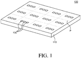
- FIG. 1 is a schematic perspective view of a display device according to one or more embodiments of the present invention.
- a display device 100 includes a substrate 110 and a plurality of light-emitting diodes (LEDs) 130 disposed on the substrate 110.
- LEDs light-emitting diodes
- the substrate 110 is for supporting elements on the display device 100 and may be an insulating substrate.
- the substrate 110 may be made of a transparent material such as glass and a resin.
- the substrate 110 may include a polymer or a plastic material.
- the substrate 110 may be made of a plastic material having flexibility.
- the substrate 110 On the substrate 110, pixel areas are defined.
- the substrate 110 may be a thin-film transistor (TFT) array substrate, and the plurality of LEDs 130 and thin-film transistors and a variety of lines for driving the LEDs 130 may be formed in the pixel area P on the upper surface of the substrate 110.
- TFT thin-film transistor
- the thin-film transistors When the thin-film transistors are turned on, driving signals input from an external device through the lines are applied to the LEDs 130, so that the LEDs 130 emit light to display an image.
- an extended light path layer that can convert the color of light and can extend the light path is disposed above the LEDs 130 for allowing the sub-pixels to emit light of red, green or blue lights.
- the extended light path layer will be described in more detail with reference to FIGS. 2 to 6 .
- the LEDs 130 may be formed via a process different from the TFT array process of the substrate 110 or may be formed on the substrate 110 of the display device 100 on which the thin-film transistors are disposed.
- the LEDs 130 of the display device 100 may be LEDs having a size of 10 to 100 ⁇ m, i.e., LEDs in micro size.
- the size of the LEDs as referred to herein, may be a size of any dimension of the LEDs, such as a height, width, or length of the LEDs.
- the LEDs may have a size of each of a height, width, and length that is within a range from 10 to 100 ⁇ m.
- the LEDs 130 may be formed by growing a plurality of thin films of an inorganic material such as Al, Ga, N, P, As and In on a sapphire substrate or a silicon substrate and then cutting or separating the sapphire substrate or the silicon substrate, or may be formed by growing a thin film on the substrate 110 where thin-film transistors are disposed. Since the LEDs 130 can be formed in a small size, they can be formed on a flexible substrate such as a plastic substrate. In addition, unlike an organic emissive layer, the LEDs 130 are formed by growing an inorganic material as thin films and thus the fabricating process is simple and the yield can be improved. In addition, the LEDs 130 made of an inorganic material have a high brightness and a long lifetime as compared with the LED made of an organic light-emitting material.
- an inorganic material such as Al, Ga, N, P, As and In
- the pixel areas P may be defined by a plurality of gate lines and a plurality of data lines.
- the gate lines and the data lines are electrically connected to the LEDs 130.
- Gate pads and data pads connected to an external source are disposed at the ends of the gate lines and the data lines, respectively, so that external signals are applied to the LEDs 130 through the gate lines and the data lines, and accordingly the LEDs 130 emit light.
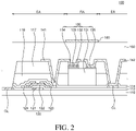
- FIG. 2 is a cross-sectional view showing a structure of a display device according to an example not forming part of the present invention.
- FIGS. 3A to 3C are perspective views of extended light path layers and reflective layers of display devices according to examples not forming part of the present invention.
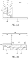
- FIGS. 4A and 4B are cross-sectional views showing a display device according to examples not forming part of the present invention.
- a thin-film transistor 120 is formed on the substrate 110.
- the thin-film transistor 120 includes a gate electrode 121, an active layer 122, a source electrode 123, and a drain electrode 124.
- a gate electrode 121 is disposed on the substrate 110, and the active layer 122 is disposed on the gate electrode 121.
- a gate insulating layer 113 for insulating the active layer 121 from the gate electrode 121 is disposed between the gate electrode 121 and the active layer 122.
- the source electrode 123 and the drain electrode 124 are disposed on the active layer 122, and a passivation layer 114 is disposed on the source electrode 123 and the drain electrode 124 for protecting the thin-film transistor 120.
- a hole may be formed in the passivation layer 114 to expose a part of the source electrode 123 of the thin-film transistor 120.
- the passivation layer 114 may be eliminated.
- a bottom-gate transistor is shown in FIG. 2 , the present invention is not limited thereto. That is to say, a thin-film transistor having a variety of structures such as a top-gate thin-film transistor as well as a bottom-gate transistor can be applied.
- a gate line GL is formed on the same layer as the gate electrode 121.
- the gate line GL may be made of the same material as the gate electrode 121.
- the data line DL may be formed in the same manner as the gate line GL.
- a common line CL is disposed on the gate insulating layer 113.
- the common line CL is for applying a common voltage to the LED 130 and may be disposed apart from the gate line GL or the data line DL.
- the common line CL may be extended in the same direction as the gate line GL or the data line DL.
- the common line CL may be made of the same material as the source electrode 123 and the drain electrode 124 as shown in FIG. 2 .
- the common line CL may be made of the same material as the gate electrode 121 as well.
- the passivation layer 114 is formed on the common line CL, with a hole formed therein, via which a part of the common line CL is exposed.
- the LED 130 is disposed on the gate insulating layer 113 or the passivation layer 114.
- an adhesive layer may be disposed on the passivation layer 114 to reinforce the adhesion of the LED 130 disposed on the passivation layer 114.
- the adhesive layer may be disposed when the LED 130 is grown on a donor substrate and then transferred onto the substrate 110 of the display device 100. When the LED 130 is grown directly on the substrate 110 of the display device 100, the adhesive layer may be eliminated.
- the LED 130 shown in FIG. 2 is an LED 130 having a lateral structure and includes an n-type layer 131, an active layer 132, a p-type layer 133, an n-electrode 135 and a p-electrode 134.
- the LED 130 having the lateral structure is employed as the LED 130, but the structure of the LED 130 is not limited thereto.
- the LED 130 is electrically connected to the thin-film transistor 120, but they are not overlapped.
- the n-type layer 131 may be formed by implanting n-type impurity into gallium nitride having good crystallinity.
- the active layer 132 is disposed on the n-type layer 131.
- the active layer 132 is an emissive layer of the LED 130 that emits light and may be formed of a nitride semiconductor, for example, indium gallium nitride.
- the p-type layer 133 is disposed on the active layer 132.
- the p-type layer 133 may be formed by implanting p-type impurity into gallium nitride. It is, however, to be understood that the n-type layer 131, the active layer 132 and the p-type layer 133 are not limited thereto.
- a predetermined portion may be etched out, and then the n-electrode 135 and the p-electrode 134 may be formed.
- the predetermined portion is a space for separating the n-electrode 135 from the p-electrode 134.
- the predetermined portion may be etched out so that a part of the n-type layer 131 is exposed.
- the surface of the LED 130 on which the n-electrode 135 and the p-electrode 134 are disposed is not flat, and the n-electrode 135 and the p-electrode 134 may have different levels.
- the n-electrode 135 may be disposed on the etched portion, i.e., on the n-type layer 131 that is exposed via an etching process.
- the n-electrode 135 may be made of a conductive material, for example, a transparent conductive oxide.
- the p-electrode 134 may be disposed on the non-etched region, that is, on the p-type layer 133.
- the p-electrode 134 may be made of a conductive material, for example, a transparent conductive oxide.
- the p-electrode 134 may be made of the same material as the n-electrode 135.
- a first planarization layer 116 and a second planarization layer 117 are formed on the upper surface of the substrate 110.
- the first planarization layer 116 is disposed to provide a flat surface over the thin-film transistor 120.
- the first planarization layer 116 may be formed except the region where the LED 130 is disposed and contact holes to provide a flat surface.
- the second planarization layer 117 may be disposed on the first planarization layer 116.
- the second planarization layer 117 may be disposed over the thin-film transistor 120 and the LED 130 except the contact holes.
- the second planarization layer 117 may be formed such that a part of the p-electrode 134 and a part of the n-electrode 135 of the LED 130 are opened.
- the display device 100 includes two planarization layers in the example shown in FIG. 2 , this is merely illustrative. If a single planarization is formed, the processing time may be too long. Accordingly, by disposing the two planarization layers, it is possible to reduce the processing time. Accordingly, the planarization layers 116 and 117 are not necessarily formed as a plurality of layers as shown in FIG. 2 , but may be formed as a single planarization layer.
- the first electrode 141 is disposed to electrically connect the thin-film transistor 120 with the p-electrode 134 of the LED.
- the first electrode 141 is electrically connected to the source electrode 123 of the thin-film transistor 120 through a contact hole formed through first planarization layer 116, the second planarization layer 117 and the passivation layer 114, and is electrically connected to the p-electrode 134 of the LED 130 through a contact hole formed through the second planarization layer 117. It is, however, to be understood that the present invention is not limited thereto.
- the first electrode 141 may be electrically connected to the drain electrode 124 of the thin-film transistor 120 depending on the type of the thin-film transistor.
- the second electrode 142 is an electrode for connecting the common line CL with the n-electrode 135 of the LED 130.
- the second electrode 142 is electrically connected to the common line CL through a contact hole formed through first planarization layer 116, the second planarization layer 117 and the passivation layer 114, and is electrically connected to the n-electrode 135 of the LED 130 through a contact hole formed through the second planarization layer 117.
- the display device 100 when the display device 100 is turned on, different voltage levels applied to the source electrode 123 of the thin-film transistor 120 and the common line CL are applied to the p-electrode 134 and the n-electrode 135 through the first electrode 141 and the second electrode 142, respectively, such that the LED 130 can emit light.
- the thin-film transistor 120 is electrically connected to the p-electrode 134 and the common line CL is electrically connected to the n-electrode 135 in the example shown in FIG. 2 , this is merely illustrative.
- the thin-film transistor 120 may be electrically connected to the n-electrode 135 and the common line CL may be electrically connected to the p-electrode 134.
- An extended light path layer 150 is disposed above the thin-film transistor 120 and the LED 130.
- the extended light path layer 150 prevents leakage of light emitted from the LED 130 and improves luminous efficiency.
- the extended light path layer 150 may be made of a transparent resin such as polymethylmetacrylate (PMMA), polyethylene terephthlate (PET), poly carbonate (PC) and polyethylene naphthalate (PEN).
- the extended light path layer 150 further includes a color conversion material, for example, quantum dots or a fluorescent material. Accordingly, in the display device 100 according to one or more embodiments of the present invention, the blue light emitted from the LED 130 can be converted into the light of the wavelength of each of the sub-pixels, i.e., into red light in a red sub-pixel and green light in a green sub-pixel by the color conversion material contained in the extended light path layer 150.
- a color conversion material for example, quantum dots or a fluorescent material.
- Different color conversion materials may be contained in the extended light path layer 150 of different sub-pixels.
- the color conversion material included in the extended light path layer 150 disposed in a red sub-pixel is a first color conversion material
- the color conversion material included in the extended light path layer 150 disposed in a green sub-pixel may be a second color conversion material different from the first color conversion material.
- the extended light path layer 150 disposed in a blue sub-pixel may contain no color conversion material.
- a proportion of the color conversion material contained in the light path enlargement of a sub-pixel may be different from that of another sub-pixel. For example, if the color conversion material contained in the extended light path layer 150 of a red sub-pixel has a first proportion, the color conversion material contained in the extended light path layer 150 of a green sub-pixel may have a second proportion.
- the extended light path layer 150 may further include a diffusing agent.
- the diffusing agent may be added during the process of forming a transparent base material of the extended light path layer 150, or may be included in the extended light path layer 150 by printing or coating it onto the transparent base material after it is formed.
- the diffusing agent may be, for example, silica, aluminum hydroxide, aluminum oxide, zinc oxide, acrylic, polyurethane, polyvinyl chloride series, etc.
- the extended light path layer 150 includes the diffusing agent so that the light can be diffused by the diffusing agent after the wavelength is converted and can exit to the outside.
- the diffusing agent included in the light path enlargement may have different proportions for different sub-pixels.
- the diffusing agent included in the extended light path layer 150 of a red sub-pixel has a first proportion
- the diffusing agent included in the extended light path layer 150 of a green sub-pixel may have a second proportion.
- no diffusing agent may be included in the extended light path layer 150 of some sub-pixels.
- the extended light path layer 150 disposed in each of a red sub-pixel and a green sub-pixel may further include a light absorbing agent capable of absorbing light of a certain wavelength band to improve the color gamut.
- the light absorbing agent can absorb light in the wavelength band between the red light emitted from the red sub-pixel and the green light emitted from the green sub-pixel, allowing for pure red and green to be displayed or transmitted by the extended light path layer 150.
- the light absorbing agent can absorb light in the wavelength band between the blue light emitted from the blue sub-pixel and the green light emitted from the green sub-pixel, allowing for pure and green and blue to be displayed or transmitted by the extended light path layer 150.
- the light absorbing agent may be, for example, at least one of fluorescent quencher selected from fluorescent dyes of cyanine, rhodamine and porphyrin series.
- the LEDs 130 disposed in the sub-pixels of the display device 100 may be LEDs emitting the light of the same color.
- the LEDs 130 emit blue light B
- the extended light path layer 150 including a color conversion material capable of converting the blue light into red and green lights is disposed above the LEDs 130, such that red sub-pixels, green sub-pixels, and blue sub-pixels can be formed.
- a black matrix may be disposed to prevent color mixing among the red sub-pixel, the green sub-pixel, and the blue sub-pixel.
- the extended light path layer 150 may be extended from the thin-film transistor 120 to the second electrode 142 electrically connected to the common line CL including the LED 130.
- the extended light path layer 150 may cover the thin-film transistor 120, the LED 130, and the second electrode 142.
- the extended light path layer 150 may surround a sub-pixel area for which it is disposed.
- the extended light path layer 150 may surround a sub-pixel area of the substrate 110 corresponding to an area of a sub-pixel in which a thin-film transistor 120, LED 130, and the second electrode 142 are disposed.
- the extended light path layer 150 may have a planar shape extended in the horizontal direction of the sub-pixels.
- FIG. 4A shows a Comparative Example of a display device which is illustrated for comparison with one or more embodiments of the present invention.
- a color conversion layer 50 is disposed to allow LEDs 130 to emit light of different colors in different sub-pixels.
- the color conversion layer 50 is disposed where the LEDs 130 are disposed. That is to say, the thin-film transistor which does not overlap with the LED 130 may be disposed in a nonemission area NEA while the LED 130 is disposed in an emission area EA.
- a light guide area (LGA) in which light emitted from the LED 130 is guided can be formed only in the area where the LED 130 is disposed.
- the emission area EA is substantially identical to the light guide area LGA in the comparative example display device.
- the extended light path layer 150 is disposed not only over the LED 130 but also in the area where the thin-film transistors disposed (e.g., laterally adjacent to the LED 130 on the substrate 110) which does not overlap with the LED 130.
- the extended light path layer 150 may be disposed to surround the pixel area in the horizontal direction of the pixel area in which the pixels are arranged. More specifically, the LED 130 and the thin-film transistor are disposed in the pixel area, and the extended light path layer 150 is disposed from the LED 130 to the area where the thin-film transistor is disposed.
- the extended light path layer 150 serves as a light path for guiding light emitted from the LED 130, and the area where the extended light path layer 150 is disposed is the light guide area (LGA). That is to say, in the display device 100 according to embodiments of the present invention, the path of the light emitted from the LED 130 becomes long or extended along a first direction, which may be a direction parallel to a surface of the substrate, for example, along which the thin-film transistor and the LED 130 are disposed (e.g., in the horizontal direction as shown in FIG. 4B ). As described above, the display device 100 according to some embodiments of the present invention can increase the luminous efficiency of the display device 100 by extending the path of the light emitted from the LED 130 in the horizontal direction.
- the extended light path layer 150 extends the path of the light in the horizontal direction of the sub-pixels 150R, 150G and 150B, it is possible to reduce the thickness of the display device 100.
- a reflective layer 160 is disposed on the extended light path layer 150.
- the reflective layer 160 may be disposed on the extended light path layer 150 in line with the LED 130, for example, the reflective layer 160 overlaps the LED 130 and may be aligned with the LED 130 along a direction (e.g., a vertical direction) transverse to the extension direction of the extended light path layer 150.
- the reflective layer 160 may be made of any reflective material, and in some embodiments, the reflective layer 160 may be made of a metal material such as titanium dioxide (TiO 2 ). By disposing the reflective layer 160, it is possible to suppress leakage of light emitted from the LED 130 to the outside.
- the reflective layer 160 may be disposed to surround at least one surface of each sub-pixel.
- the reflective layer 160 may be disposed to surround four or three faces of the side surfaces of each sub-pixel, as shown in FIGS. 3A and 3B .
- the reflective layer 160 is formed on the extended light path layer 150 in line with the LED 130, i.e., in a reflection area RA. It may be disposed to surround the upper surface and the three side surfaces of each of the sub-pixels 150R, 150G, and 150B. Accordingly, it is possible to suppress leakage of light emitted from the LED 130 to the outside, and more light can be emitted in the emission area EA.
- the reflective layer 160 is formed on the extended light path layer 150 in line with the LED 130, i.e., in a reflective area RA. It may be disposed to surround the upper surface and two side surfaces of each of the sub-pixels 150R, 150G, and 150B. Accordingly, it is possible to suppress leakage of light emitted from the LED 130 to the outside, and more light can be emitted in the emission area EA.
- the sub-pixels R, G and B may have a cuboid shape extended in the horizontal direction, i.e., in the longitudinal direction as shown in FIGS. 3A and 3B or may have a circular, cylindrical, disc, or dome shape as shown in FIG. 3C .
- FIGS. 3A and 3B illustrate a rectangular parallelepiped shape, this is merely illustrative. They may have a lenticular lens shape extended in the horizontal direction.
- the reflective layer 160 may be disposed on the upper surface of the extended light path layer 150 in line with the LED 130 for each of the sub-pixels R, G and B.
- the extended light path layer 150 may be formed as follows: a mold having a size equal to or slightly larger than the size of the extended light path layer 150 is prepared. Then, the mold is filled with a transparent resin. A press jig is placed above the extended light path layer 150. It is pressed with the press jig, such that the extended light path layer 150 having a planar shape (e.g., a planar upper surface) can be formed.
- a planar shape e.g., a planar upper surface
- the emission area EA and the reflection area RA may be defined on the substrate 110 by the extended light path layer 150 and the reflective layer 160.
- the emission area EA In the emission area EA, light emitted from the LED 130 exits.
- the emission area EA is in line with (or may overlap) the thin-film transistor 120. That is, the emission area EA may overlap the thin-film transistor 120, and further may extend laterally (e.g., horizontally) beyond edges of the thin-film transistor 120, since the extended light path layer 150 may completely overlap and may extend beyond edges of the thin-film transistor 120.
- the second electrode 142 may also be disposed in the emission area EA.
- the extended light path layer 150 is extended in the horizontal direction of the sub-pixels, so that the emission area is extended compared to an existing display device where the emission area is formed only in line with the LED, thereby increasing the luminous efficiency.
- the reflection area RA In the reflection area RA, light emitted from the LED 130 is reflected by the reflective layer 160 back into the extended light path layer 150.
- the reflection area RA may be in line with the reflective layer 160.
- a passivation layer may be further disposed on the extended light path layer 150 and the reflective layer 160.
- FIG. 5 is a cross-sectional view showing a structure of a display device according to an example not forming part of the present invention.
- a display device 100 may include a thin-film transistor 120, an LED 130, a first electrode 141, a second electrode 142, an extended light path layer 150, a first reflective layer 540, and a second reflective layer 160.
- the display device 100' is substantially identical to the display device 100 shown in FIG. 2 except that the first reflective layer 540 is further disposed; and, therefore, the redundant description will be omitted.
- the first reflective layer 540 is disposed on the passivation layer 114 disposed on the thin-film transistor 120.
- the first reflective layer 540 reflects light emitted from the LED 130 toward the substrate 110 toward the upper side of the display device 100 and guides the light to the outside of the display device 100.
- the first reflective layer 540 may be made of a metal material having a high reflectivity.
- the LED 130 may be disposed on the first reflective layer 540, and the extended light path layer 150 and the second reflective layer 160 may be disposed above the LED 130.
- an adhesive layer may be further disposed between the first reflective layer 540 and the LED 130 to reinforce the adhesion therebetween.
- the adhesive layer may be disposed when the LED 130 is grown on a donor substrate and then transferred onto the substrate 110 of the display device 100. When the LED 130 is grown directly on the substrate 110 of the display device 100, the adhesive layer may be eliminated.
- the display device 100' includes the first reflective layer 540 and the second reflective layer 160 on and under the LED 130, respectively, so that it is possible to prevent leakage of light emitted from the LED 130 and to improve the luminous efficiency of the display device.
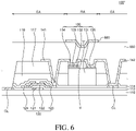
- FIG. 6 is a cross-sectional view showing a structure of a display device according to an embodiment of the present invention.
- a display device 100" includes a thin-film transistor 120, an LED 130, a first electrode 141, a second electrode 142, an extended light path layer 650, and a reflective layer 660.
- the display device 100" is substantially identical to the display device 100 shown in FIG. 2 except that an extended light path layer and a reflective layer have different shapes; and, therefore, the redundant description will be omitted.
- an extended light path layer 650 including a groove V is disposed above the LED 130.
- the groove V is disposed in line with (e.g., aligned or overlapping with) the LED 130.
- the groove V may be formed in the extended light path layer 650 with a predetermined angle.
- the path of the light emitted from the LED 130 can be changed by the side surface of the groove V having the predetermined angle.
- the groove V formed in the extended light path layer 650 can scatter light emitted from the LED 130, thereby improving the luminous efficiency of the display device.
- the groove V is shown as having a cup shape in FIG.
- the shape of the groove V is not particularly limited as long as the luminous efficiency can be improved.
- the single groove V is formed in the extended light path layer 650 in FIG. 6 . It is, however, to be understood that the present invention is not limited thereto. More than one grooves V may be formed. If a number of grooves V are formed in the extended light path layer 650, the path of the light emitted from the LED 130 can be changed several times, and thus the light can propagate more widely and evenly so that the luminous efficiency can be further improved.
- the reflective layer 660 may be disposed conforming to the shape of the groove V.
- the reflective layer 660 may also be disposed in line with the LED 130.
- the display device 100" includes the extended light path layer 650 having the groove V in line with the LED 130, and the reflective layer 660 formed on the extended light path layer 650 along the shape of the groove V, so that the outcoupling efficiency can be further improved.
- FIGS. 7A and 7B are graphs for illustrating luminous efficiency of a display device according to one or more embodiments of the present invention.
- the graph shows the luminous efficiency depending on the concentration of the color conversion material in the extended light path layer 150.
- Curve a represents the luminous efficiency of the extended light path layer containing 0.1 g of a color conversion material in 22 ml of a transparent base material.
- Curve b represents the luminous efficiency of the extended light path layer containing 0.3 g of a color conversion material in 22 ml of a transparent base material.
- Curve c represents the luminous efficiency of the extended light path layer containing 0.5 g of a color conversion material in 22 ml of a transparent base material.
- Curve d represents the luminous efficiency of the extended light path layer containing 0.7 g of a color conversion material in 22 ml of a transparent base material.
- the luminous efficiency is improved as the concentration of the color conversion material contained in the extended light path layer 150 is decreased. It is, however, to be noted that the luminous efficiency may vary depending on the kind of the color conversion material. As described above, the color conversion material may be made of a phosphor or quantum dots. If the concentration is too low, the luminous efficiency may be rather poor depending on which of the phosphor, quantum dots and other color conversion materials is contained in the extended light path layer 150. Accordingly, there may be an optimal lowest point. For example, assuming that 22 ml of the transparent base material is included in the extended light path layer, the lowest point of the color conversion material may be 0.1 g. In FIG.
- the lowest point of the conversion material may be 0.1 g in some embodiments.
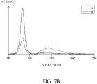
- FIG. 7B is a graph showing the luminous efficiency depending on the light path.
- Curve a represents the luminous efficiency of a comparative example display device
- Curve b represents the luminous efficiency of the display device according to an embodiment of the present invention.
- Curve a represents good luminous efficiency only in a particular wavelength band, especially a wavelength band from 400 to 480 nm, i.e., only in the blue wavelength band, while it represents poor luminous efficiency in the other wavelength bands.
- the red sub-pixels, the green sub-pixels and the blue sub-pixels include LEDs of the same color and the color conversion layer is disposed above them, the blue LEDs are usually employed. Consequently, the luminous efficiency is good in the blue wavelength band.
- Curve b exhibits that the luminous efficiency is also good in the other wavelength bands, i.e., the green wavelength band. Accordingly, it can be seen that the luminous efficiency is better on average as the light path is longer, like in the display device 100 according to one or more embodiments of the present invention.
Landscapes
- Devices For Indicating Variable Information By Combining Individual Elements (AREA)
- Electroluminescent Light Sources (AREA)
Description
- The present disclosure relates to a display device, and more particularly to a display device using light-emitting diodes (LEDs).
- Liquid-crystal display devices (LCDs) and organic light-emitting display devices, which have been widely used up to now, find more and more applications.
- Liquid-crystal display devices and organic light-emitting display devices are widely employed as the screen of typical electronic devices such as mobile phones and laptop computers because they can provide high resolution image and can be made thin and light.
- However, liquid-crystal display devices and organic light-emitting display devices include a bezel that is seen by a viewer and does not display an image, and thus the display area is reduced by the size of the bezel. For example, a liquid-crystal display device requires a sealant used to seal the liquid-crystal molecules and to attach the upper substrate and the lower substrate together, and thus there are limitations in decreasing the size of the bezel. In addition, an organic light-emitting display device typically includes an encapsulation layer to protect organic light-emitting diodes (OLEDs) since the OLEDs are made of an organic material and thus are very vulnerable to moisture or oxygen. There are limitations in decreasing the size of the bezel.
- In view of such shortcomings of liquid-crystal display devices and organic light-emitting display devices, display devices including LEDs have been proposed. LEDs are made of an inorganic material rather than an organic material and thus are more reliable. Accordingly, display devices including LEDs have a long lifetime as compared with liquid-crystal display devices or organic light-emitting display devices. In addition, the LEDs can be turned on and off quickly, consume less power, are robust to impact resistance and stable, and can display a high-brightness image. Accordingly, LEDs are advantageous for large screens.
-
US 2017/263672 A1 discloses a display device including a substrate having a sub-pixel area in which a LED and a transistor is disposed. A light guiding layer including a color conversion material is disposed in the sub-pixel area over the LED and the transistor. A reflective metal electrode is disposed to cover a top portion of the LED and the light guiding layer. -
EP 3343273 A2 discloses a display device including a substrate having a sub-pixel area in which a LED and a transistor is disposed. A layer including a color conversion material is disposed in the sub-pixel area over the LED and the transistor. A black matrix and filter layer is disposed over the color conversion layer. - In order to fabricate a display device including such LEDs, a single pixel is implemented by using three LEDs including red (R), green (G) and blue (B) LEDs. However, in order to implement a pixel by using three LEDs, there are many processes such as a process of growing each of the LEDs on a donor substrate and a process of transferring the LEDs grown on the donor substrate to the substrate of the display device. As a result, there is a problem that color deviations occur due to a process failure or depending on a temperature and an environment.
- Previously, only the blue LEDs are grown on the donor substrate or directly grown on the substrate of a display device, and the color conversion layer including quantum dots that can represent red and green colors is disposed to change the wavelength so that light of red and green colors are represented.
- The inventors of the present invention have recognized that it is advantageous to increase the light path in order to prevent leakage of blue light and improve the efficiency of the color conversion layer when only the blue LEDs are used as described above.
- In order to increase the light path in a display device using LEDs, the thickness of the color conversion layer may be increased. However, there are process limitations in increasing the thickness of the color conversion layer. More specifically, a color conversion layer that converts the color of light emitted from a blue LED into red or green is typically formed by using a photolithography (PR) process. By using the photolithography process, the thickness of approximately 3 µm can be achieved by spin coating, which is insufficient. Further, in order to increase the thickness of the color conversion layer, a high-viscosity photoresist should be used, which may decrease uniformity and processibility.
- In view of the above, the inventors of the present invention have devised a display device that can increase the light path without increasing the thickness of the color conversion layer.
- In some embodiments, the present invention provides a display device capable of improving the display efficiency of a display device by way of increasing the light path.
- In some embodiments, the present invention provides a display device having a smaller thickness by way of decreasing the thickness of a color conversion layer.
- The present invention provides a display device according to claim 1. Further embodiments are described in the dependent claims.
- The above and other aspects, features and other advantages of the present invention will be more clearly understood from the following detailed description taken in conjunction with the accompanying drawings, in which:
-
FIG. 1 is a schematic perspective view of a display device according to one or more embodiments of the present invention. -
FIG. 2 is a cross-sectional view showing a structure of a display device according to an example not forming part of the present invention. -
FIGS. 3A to 3C are perspective views of extended light path layers and reflective layers of display devices according to various examples not forming part of the present invention. -
FIGS. 4A and 4B are cross-sectional views showing a display device according to examples not forming part of the present invention. -
FIG. 5 is a cross-sectional view showing a structure of a display device according to an example not forming part of the present invention. -
FIG. 6 is a cross-sectional view showing a structure of a display device according to an embodiment of the present invention. -
FIGS. 7A and7B are graphs for illustrating luminous efficiency of a display device according to embodiments of the present invention. - Advantages and characteristics of the present invention and a method of achieving the advantages and characteristics will be clear by referring to the embodiments described below in detail together with the accompanying drawings. However, the present invention is not limited to the embodiments described herein but will be implemented in various forms. The embodiments are provided by way of example only so that a person of ordinary skilled in the art can fully understand the description of the present invention. Therefore, the scope of the present invention is defined only by the appended claims.
- The shapes, sizes, ratios, angles, numbers, and the like illustrated in the accompanying drawings for describing the various embodiments of the present invention are merely examples, and the present invention is not limited thereto. Like reference numerals generally denote like elements throughout the specification. Further, in the following description of the present invention, a detailed explanation of known related technologies may be omitted to avoid unnecessarily obscuring the subject matter of the present invention. The terms such as "including," "having," and "comprising" used herein are generally intended to allow other components to be added unless the terms are used with the term "only". Any references to singular may include plural unless expressly stated otherwise.
- Components are interpreted to include an ordinary error range (e.g., a tolerance range) even if not expressly stated.
- When the position relation between two elements is described using the terms such as "on", "above", "below", and "next", one or more elements may be positioned between the two parts unless the terms are used with the term "immediately" or "directly".
- Although the terms "first," "second," and the like are used for describing various components, these components are not confined by these terms. These terms are merely used for distinguishing one component from the other components. Therefore, a first component to be mentioned below may be a second component in a technical concept of the present invention.
- Hereinafter, various embodiments of the present invention will be described in detail with reference to accompanying drawings.
-
FIG. 1 is a schematic perspective view of a display device according to one or more embodiments of the present invention. - Referring to
FIG. 1 , adisplay device 100 according to one or more embodiments of the present invention includes asubstrate 110 and a plurality of light-emitting diodes (LEDs) 130 disposed on thesubstrate 110. - The
substrate 110 is for supporting elements on thedisplay device 100 and may be an insulating substrate. For example, thesubstrate 110 may be made of a transparent material such as glass and a resin. In addition, thesubstrate 110 may include a polymer or a plastic material. In some embodiments, thesubstrate 110 may be made of a plastic material having flexibility. - On the
substrate 110, pixel areas are defined. Although not shown in the drawings, thesubstrate 110 may be a thin-film transistor (TFT) array substrate, and the plurality ofLEDs 130 and thin-film transistors and a variety of lines for driving theLEDs 130 may be formed in the pixel area P on the upper surface of thesubstrate 110. When the thin-film transistors are turned on, driving signals input from an external device through the lines are applied to theLEDs 130, so that theLEDs 130 emit light to display an image. - Three sub-pixels emitting light of red (R), green (G) and blue (B), respectively, are arranged in each pixel area P of the
substrate 110, and anLED 130 emitting light of the same color is disposed in each sub-pixel. As theLEDs 130 emitting light of the same color are disposed in the sub-pixels of thedisplay device 100, an extended light path layer that can convert the color of light and can extend the light path is disposed above theLEDs 130 for allowing the sub-pixels to emit light of red, green or blue lights. The extended light path layer will be described in more detail with reference toFIGS. 2 to 6 . - According to one or more embodiments of the present invention, the
LEDs 130 may be formed via a process different from the TFT array process of thesubstrate 110 or may be formed on thesubstrate 110 of thedisplay device 100 on which the thin-film transistors are disposed. - According to some embodiments of the present invention, the
LEDs 130 of thedisplay device 100 may be LEDs having a size of 10 to 100 µm, i.e., LEDs in micro size. The size of the LEDs, as referred to herein, may be a size of any dimension of the LEDs, such as a height, width, or length of the LEDs. In some embodiments, the LEDs may have a size of each of a height, width, and length that is within a range from 10 to 100 µm. TheLEDs 130 may be formed by growing a plurality of thin films of an inorganic material such as Al, Ga, N, P, As and In on a sapphire substrate or a silicon substrate and then cutting or separating the sapphire substrate or the silicon substrate, or may be formed by growing a thin film on thesubstrate 110 where thin-film transistors are disposed. Since theLEDs 130 can be formed in a small size, they can be formed on a flexible substrate such as a plastic substrate. In addition, unlike an organic emissive layer, theLEDs 130 are formed by growing an inorganic material as thin films and thus the fabricating process is simple and the yield can be improved. In addition, theLEDs 130 made of an inorganic material have a high brightness and a long lifetime as compared with the LED made of an organic light-emitting material. - Although not shown in the drawings, the pixel areas P may be defined by a plurality of gate lines and a plurality of data lines. The gate lines and the data lines are electrically connected to the
LEDs 130. Gate pads and data pads connected to an external source are disposed at the ends of the gate lines and the data lines, respectively, so that external signals are applied to theLEDs 130 through the gate lines and the data lines, and accordingly theLEDs 130 emit light. -
FIG. 2 is a cross-sectional view showing a structure of a display device according to an example not forming part of the present invention.FIGS. 3A to 3C are perspective views of extended light path layers and reflective layers of display devices according to examples not forming part of the present invention.FIGS. 4A and 4B are cross-sectional views showing a display device according to examples not forming part of the present invention. - Referring to
FIG. 2 , a thin-film transistor 120 is formed on thesubstrate 110. The thin-film transistor 120 includes agate electrode 121, anactive layer 122, asource electrode 123, and adrain electrode 124. Specifically, agate electrode 121 is disposed on thesubstrate 110, and theactive layer 122 is disposed on thegate electrode 121. Agate insulating layer 113 for insulating theactive layer 121 from thegate electrode 121 is disposed between thegate electrode 121 and theactive layer 122. Thesource electrode 123 and thedrain electrode 124 are disposed on theactive layer 122, and apassivation layer 114 is disposed on thesource electrode 123 and thedrain electrode 124 for protecting the thin-film transistor 120. A hole may be formed in thepassivation layer 114 to expose a part of thesource electrode 123 of the thin-film transistor 120. In some implementations, thepassivation layer 114 may be eliminated. Although a bottom-gate transistor is shown inFIG. 2 , the present invention is not limited thereto. That is to say, a thin-film transistor having a variety of structures such as a top-gate thin-film transistor as well as a bottom-gate transistor can be applied. - A gate line GL is formed on the same layer as the
gate electrode 121. The gate line GL may be made of the same material as thegate electrode 121. Although the gate line GL is shown inFIG. 2 , the data line DL may be formed in the same manner as the gate line GL. - A common line CL is disposed on the
gate insulating layer 113. The common line CL is for applying a common voltage to theLED 130 and may be disposed apart from the gate line GL or the data line DL. In addition, the common line CL may be extended in the same direction as the gate line GL or the data line DL. The common line CL may be made of the same material as thesource electrode 123 and thedrain electrode 124 as shown inFIG. 2 . However, the common line CL may be made of the same material as thegate electrode 121 as well. Thepassivation layer 114 is formed on the common line CL, with a hole formed therein, via which a part of the common line CL is exposed. - Referring to
FIG. 2 , theLED 130 is disposed on thegate insulating layer 113 or thepassivation layer 114. Although not shown inFIG. 2 , an adhesive layer may be disposed on thepassivation layer 114 to reinforce the adhesion of theLED 130 disposed on thepassivation layer 114. The adhesive layer may be disposed when theLED 130 is grown on a donor substrate and then transferred onto thesubstrate 110 of thedisplay device 100. When theLED 130 is grown directly on thesubstrate 110 of thedisplay device 100, the adhesive layer may be eliminated. - The
LED 130 shown inFIG. 2 is anLED 130 having a lateral structure and includes an n-type layer 131, anactive layer 132, a p-type layer 133, an n-electrode 135 and a p-electrode 134. According to some embodiments of the present invention, theLED 130 having the lateral structure is employed as theLED 130, but the structure of theLED 130 is not limited thereto. TheLED 130 is electrically connected to the thin-film transistor 120, but they are not overlapped. - The structure of the
LED 130 will be described in more detail. The n-type layer 131 may be formed by implanting n-type impurity into gallium nitride having good crystallinity. Theactive layer 132 is disposed on the n-type layer 131. Theactive layer 132 is an emissive layer of theLED 130 that emits light and may be formed of a nitride semiconductor, for example, indium gallium nitride. The p-type layer 133 is disposed on theactive layer 132. The p-type layer 133 may be formed by implanting p-type impurity into gallium nitride. It is, however, to be understood that the n-type layer 131, theactive layer 132 and the p-type layer 133 are not limited thereto. - As described above, after the n-
type layer 131, theactive layer 132 and the p-type layer 133 are sequentially stacked, a predetermined portion may be etched out, and then the n-electrode 135 and the p-electrode 134 may be formed. The predetermined portion is a space for separating the n-electrode 135 from the p-electrode 134. The predetermined portion may be etched out so that a part of the n-type layer 131 is exposed. In other words, the surface of theLED 130 on which the n-electrode 135 and the p-electrode 134 are disposed is not flat, and the n-electrode 135 and the p-electrode 134 may have different levels. - As such, the n-
electrode 135 may be disposed on the etched portion, i.e., on the n-type layer 131 that is exposed via an etching process. The n-electrode 135 may be made of a conductive material, for example, a transparent conductive oxide. On the other hand, the p-electrode 134 may be disposed on the non-etched region, that is, on the p-type layer 133. The p-electrode 134 may be made of a conductive material, for example, a transparent conductive oxide. In addition, the p-electrode 134 may be made of the same material as the n-electrode 135. - Subsequently, a
first planarization layer 116 and asecond planarization layer 117 are formed on the upper surface of thesubstrate 110. Referring toFIG. 2 , thefirst planarization layer 116 is disposed to provide a flat surface over the thin-film transistor 120. Thefirst planarization layer 116 may be formed except the region where theLED 130 is disposed and contact holes to provide a flat surface. In addition, thesecond planarization layer 117 may be disposed on thefirst planarization layer 116. Thesecond planarization layer 117 may be disposed over the thin-film transistor 120 and theLED 130 except the contact holes. Thesecond planarization layer 117 may be formed such that a part of the p-electrode 134 and a part of the n-electrode 135 of theLED 130 are opened. Although thedisplay device 100 according to some embodiments of the present invention includes two planarization layers in the example shown inFIG. 2 , this is merely illustrative. If a single planarization is formed, the processing time may be too long. Accordingly, by disposing the two planarization layers, it is possible to reduce the processing time. Accordingly, the planarization layers 116 and 117 are not necessarily formed as a plurality of layers as shown inFIG. 2 , but may be formed as a single planarization layer. - Referring to
FIG. 2 , thefirst electrode 141 is disposed to electrically connect the thin-film transistor 120 with the p-electrode 134 of the LED. Thefirst electrode 141 is electrically connected to thesource electrode 123 of the thin-film transistor 120 through a contact hole formed throughfirst planarization layer 116, thesecond planarization layer 117 and thepassivation layer 114, and is electrically connected to the p-electrode 134 of theLED 130 through a contact hole formed through thesecond planarization layer 117. It is, however, to be understood that the present invention is not limited thereto. Thefirst electrode 141 may be electrically connected to thedrain electrode 124 of the thin-film transistor 120 depending on the type of the thin-film transistor. - The
second electrode 142 is an electrode for connecting the common line CL with the n-electrode 135 of theLED 130. Thesecond electrode 142 is electrically connected to the common line CL through a contact hole formed throughfirst planarization layer 116, thesecond planarization layer 117 and thepassivation layer 114, and is electrically connected to the n-electrode 135 of theLED 130 through a contact hole formed through thesecond planarization layer 117. - Accordingly, when the
display device 100 is turned on, different voltage levels applied to thesource electrode 123 of the thin-film transistor 120 and the common line CL are applied to the p-electrode 134 and the n-electrode 135 through thefirst electrode 141 and thesecond electrode 142, respectively, such that theLED 130 can emit light. Although the thin-film transistor 120 is electrically connected to the p-electrode 134 and the common line CL is electrically connected to the n-electrode 135 in the example shown inFIG. 2 , this is merely illustrative. The thin-film transistor 120 may be electrically connected to the n-electrode 135 and the common line CL may be electrically connected to the p-electrode 134. - An extended
light path layer 150 is disposed above the thin-film transistor 120 and theLED 130. The extendedlight path layer 150 prevents leakage of light emitted from theLED 130 and improves luminous efficiency. The extendedlight path layer 150 may be made of a transparent resin such as polymethylmetacrylate (PMMA), polyethylene terephthlate (PET), poly carbonate (PC) and polyethylene naphthalate (PEN). - The extended
light path layer 150 further includes a color conversion material, for example, quantum dots or a fluorescent material. Accordingly, in thedisplay device 100 according to one or more embodiments of the present invention, the blue light emitted from theLED 130 can be converted into the light of the wavelength of each of the sub-pixels, i.e., into red light in a red sub-pixel and green light in a green sub-pixel by the color conversion material contained in the extendedlight path layer 150. - Different color conversion materials may be contained in the extended
light path layer 150 of different sub-pixels. For example, if the color conversion material included in the extendedlight path layer 150 disposed in a red sub-pixel is a first color conversion material, the color conversion material included in the extendedlight path layer 150 disposed in a green sub-pixel may be a second color conversion material different from the first color conversion material. It is to be noted that the extendedlight path layer 150 disposed in a blue sub-pixel may contain no color conversion material. In addition, a proportion of the color conversion material contained in the light path enlargement of a sub-pixel may be different from that of another sub-pixel. For example, if the color conversion material contained in the extendedlight path layer 150 of a red sub-pixel has a first proportion, the color conversion material contained in the extendedlight path layer 150 of a green sub-pixel may have a second proportion. - In addition, the extended
light path layer 150 may further include a diffusing agent. The diffusing agent may be added during the process of forming a transparent base material of the extendedlight path layer 150, or may be included in the extendedlight path layer 150 by printing or coating it onto the transparent base material after it is formed. The diffusing agent may be, for example, silica, aluminum hydroxide, aluminum oxide, zinc oxide, acrylic, polyurethane, polyvinyl chloride series, etc. In thedisplay device 100 according to some embodiments of the present invention, the extendedlight path layer 150 includes the diffusing agent so that the light can be diffused by the diffusing agent after the wavelength is converted and can exit to the outside. In addition, the diffusing agent included in the light path enlargement may have different proportions for different sub-pixels. For example, if the diffusing agent included in the extendedlight path layer 150 of a red sub-pixel has a first proportion, the diffusing agent included in the extendedlight path layer 150 of a green sub-pixel may have a second proportion. In addition, no diffusing agent may be included in the extendedlight path layer 150 of some sub-pixels. - The extended
light path layer 150 disposed in each of a red sub-pixel and a green sub-pixel may further include a light absorbing agent capable of absorbing light of a certain wavelength band to improve the color gamut. For example, the light absorbing agent can absorb light in the wavelength band between the red light emitted from the red sub-pixel and the green light emitted from the green sub-pixel, allowing for pure red and green to be displayed or transmitted by the extendedlight path layer 150. Alternatively, the light absorbing agent can absorb light in the wavelength band between the blue light emitted from the blue sub-pixel and the green light emitted from the green sub-pixel, allowing for pure and green and blue to be displayed or transmitted by the extendedlight path layer 150. The light absorbing agent may be, for example, at least one of fluorescent quencher selected from fluorescent dyes of cyanine, rhodamine and porphyrin series. - As described above, the
LEDs 130 disposed in the sub-pixels of thedisplay device 100 according to some embodiments of the present invention may be LEDs emitting the light of the same color. For example, according to one or more embodiments of the present invention, theLEDs 130 emit blue light B, and the extendedlight path layer 150 including a color conversion material capable of converting the blue light into red and green lights is disposed above theLEDs 130, such that red sub-pixels, green sub-pixels, and blue sub-pixels can be formed. In addition, although not shown in the drawings, a black matrix may be disposed to prevent color mixing among the red sub-pixel, the green sub-pixel, and the blue sub-pixel. - The extended
light path layer 150 may be extended from the thin-film transistor 120 to thesecond electrode 142 electrically connected to the common line CL including theLED 130. In some embodiments, the extendedlight path layer 150 may cover the thin-film transistor 120, theLED 130, and thesecond electrode 142. In some embodiments, the extendedlight path layer 150 may surround a sub-pixel area for which it is disposed. For example, the extendedlight path layer 150 may surround a sub-pixel area of thesubstrate 110 corresponding to an area of a sub-pixel in which a thin-film transistor 120,LED 130, and thesecond electrode 142 are disposed. Referring toFIGS. 3A to 3C , the extendedlight path layer 150 may have a planar shape extended in the horizontal direction of the sub-pixels. By virtue of the extendedlight path layer 150, thedisplay device 100 according to some embodiments of the present invention may have a longer path of light emitted from theLEDs 130. -
FIG. 4A shows a Comparative Example of a display device which is illustrated for comparison with one or more embodiments of the present invention. As shown inFIG. 4A , in the comparative example display device, acolor conversion layer 50 is disposed to allowLEDs 130 to emit light of different colors in different sub-pixels. Thecolor conversion layer 50 is disposed where theLEDs 130 are disposed. That is to say, the thin-film transistor which does not overlap with theLED 130 may be disposed in a nonemission area NEA while theLED 130 is disposed in an emission area EA. Accordingly, in the comparative example display device, a light guide area (LGA) in which light emitted from theLED 130 is guided can be formed only in the area where theLED 130 is disposed. In other words, as shown inFIG. 4A , the emission area EA is substantially identical to the light guide area LGA in the comparative example display device. - In addition, as shown in
FIG. 4A , in order to improve luminous efficiency of light emitted from theLED 130, it has been proposed to increase the light path by increasing the thickness of thecolor conversion layer 50 in the vertical direction. However, there are limitations in increasing the thickness of thecolor conversion layer 50 in the vertical direction, and if the thickness is increased, the display device becomes thick. - In contrast, referring to
FIG. 4B showing thedisplay device 100 according to an example not forming part of the present invention, the extendedlight path layer 150 is disposed not only over theLED 130 but also in the area where the thin-film transistors disposed (e.g., laterally adjacent to theLED 130 on the substrate 110) which does not overlap with theLED 130. The extendedlight path layer 150 may be disposed to surround the pixel area in the horizontal direction of the pixel area in which the pixels are arranged. More specifically, theLED 130 and the thin-film transistor are disposed in the pixel area, and the extendedlight path layer 150 is disposed from theLED 130 to the area where the thin-film transistor is disposed. Accordingly, the extendedlight path layer 150 serves as a light path for guiding light emitted from theLED 130, and the area where the extendedlight path layer 150 is disposed is the light guide area (LGA). That is to say, in thedisplay device 100 according to embodiments of the present invention, the path of the light emitted from theLED 130 becomes long or extended along a first direction, which may be a direction parallel to a surface of the substrate, for example, along which the thin-film transistor and theLED 130 are disposed (e.g., in the horizontal direction as shown inFIG. 4B ). As described above, thedisplay device 100 according to some embodiments of the present invention can increase the luminous efficiency of thedisplay device 100 by extending the path of the light emitted from theLED 130 in the horizontal direction. - In addition, as shown in
FIGS. 3A to 3C , as the extendedlight path layer 150 extends the path of the light in the horizontal direction of the sub-pixels 150R, 150G and 150B, it is possible to reduce the thickness of thedisplay device 100. - A
reflective layer 160 is disposed on the extendedlight path layer 150. - The
reflective layer 160 may be disposed on the extendedlight path layer 150 in line with theLED 130, for example, thereflective layer 160 overlaps theLED 130 and may be aligned with theLED 130 along a direction (e.g., a vertical direction) transverse to the extension direction of the extendedlight path layer 150. Thereflective layer 160 may be made of any reflective material, and in some embodiments, thereflective layer 160 may be made of a metal material such as titanium dioxide (TiO2). By disposing thereflective layer 160, it is possible to suppress leakage of light emitted from theLED 130 to the outside. - The
reflective layer 160 may be disposed to surround at least one surface of each sub-pixel. For example, thereflective layer 160 may be disposed to surround four or three faces of the side surfaces of each sub-pixel, as shown inFIGS. 3A and3B . - Initially, as shown in
FIG. 3A , thereflective layer 160 according to the present invention is formed on the extendedlight path layer 150 in line with theLED 130, i.e., in a reflection area RA. It may be disposed to surround the upper surface and the three side surfaces of each of the sub-pixels 150R, 150G, and 150B. Accordingly, it is possible to suppress leakage of light emitted from theLED 130 to the outside, and more light can be emitted in the emission area EA. - In addition, as shown in
FIG. 3B , thereflective layer 160 according to some embodiments of the present invention is formed on the extendedlight path layer 150 in line with theLED 130, i.e., in a reflective area RA. It may be disposed to surround the upper surface and two side surfaces of each of the sub-pixels 150R, 150G, and 150B. Accordingly, it is possible to suppress leakage of light emitted from theLED 130 to the outside, and more light can be emitted in the emission area EA. - The sub-pixels R, G and B according to some embodiments of the present invention may have a cuboid shape extended in the horizontal direction, i.e., in the longitudinal direction as shown in
FIGS. 3A and3B or may have a circular, cylindrical, disc, or dome shape as shown inFIG. 3C . AlthoughFIGS. 3A and3B illustrate a rectangular parallelepiped shape, this is merely illustrative. They may have a lenticular lens shape extended in the horizontal direction. As shown inFIG. 3C , thereflective layer 160 may be disposed on the upper surface of the extendedlight path layer 150 in line with theLED 130 for each of the sub-pixels R, G and B. - The extended
light path layer 150 may be formed as follows: a mold having a size equal to or slightly larger than the size of the extendedlight path layer 150 is prepared. Then, the mold is filled with a transparent resin. A press jig is placed above the extendedlight path layer 150. It is pressed with the press jig, such that the extendedlight path layer 150 having a planar shape (e.g., a planar upper surface) can be formed. - The emission area EA and the reflection area RA may be defined on the
substrate 110 by the extendedlight path layer 150 and thereflective layer 160. - In the emission area EA, light emitted from the
LED 130 exits. The emission area EA is in line with (or may overlap) the thin-film transistor 120. That is, the emission area EA may overlap the thin-film transistor 120, and further may extend laterally (e.g., horizontally) beyond edges of the thin-film transistor 120, since the extendedlight path layer 150 may completely overlap and may extend beyond edges of the thin-film transistor 120. In addition, thesecond electrode 142 may also be disposed in the emission area EA. As described above, the extendedlight path layer 150 according to one or more embodiments of the present invention is extended in the horizontal direction of the sub-pixels, so that the emission area is extended compared to an existing display device where the emission area is formed only in line with the LED, thereby increasing the luminous efficiency. - In the reflection area RA, light emitted from the
LED 130 is reflected by thereflective layer 160 back into the extendedlight path layer 150. The reflection area RA may be in line with thereflective layer 160. By disposing the reflection area RA, leakage of light to the outside can be reduced. - Although not shown in
FIG. 2 , a passivation layer may be further disposed on the extendedlight path layer 150 and thereflective layer 160. -
FIG. 5 is a cross-sectional view showing a structure of a display device according to an example not forming part of the present invention. - Referring to
FIG. 5 , adisplay device 100 may include a thin-film transistor 120, anLED 130, afirst electrode 141, asecond electrode 142, an extendedlight path layer 150, a firstreflective layer 540, and a secondreflective layer 160. The display device 100' is substantially identical to thedisplay device 100 shown inFIG. 2 except that the firstreflective layer 540 is further disposed; and, therefore, the redundant description will be omitted. - In the display device 100', the first
reflective layer 540 is disposed on thepassivation layer 114 disposed on the thin-film transistor 120. - The first
reflective layer 540 reflects light emitted from theLED 130 toward thesubstrate 110 toward the upper side of thedisplay device 100 and guides the light to the outside of thedisplay device 100. The firstreflective layer 540 may be made of a metal material having a high reflectivity. - The
LED 130 may be disposed on the firstreflective layer 540, and the extendedlight path layer 150 and the secondreflective layer 160 may be disposed above theLED 130. Although not shown inFIG. 5 , an adhesive layer may be further disposed between the firstreflective layer 540 and theLED 130 to reinforce the adhesion therebetween. The adhesive layer may be disposed when theLED 130 is grown on a donor substrate and then transferred onto thesubstrate 110 of thedisplay device 100. When theLED 130 is grown directly on thesubstrate 110 of thedisplay device 100, the adhesive layer may be eliminated. As such, the display device 100' includes the firstreflective layer 540 and the secondreflective layer 160 on and under theLED 130, respectively, so that it is possible to prevent leakage of light emitted from theLED 130 and to improve the luminous efficiency of the display device. -
FIG. 6 is a cross-sectional view showing a structure of a display device according to an embodiment of the present invention. - Referring to
FIG. 6 , adisplay device 100" includes a thin-film transistor 120, anLED 130, afirst electrode 141, asecond electrode 142, an extendedlight path layer 650, and areflective layer 660. Thedisplay device 100" is substantially identical to thedisplay device 100 shown inFIG. 2 except that an extended light path layer and a reflective layer have different shapes; and, therefore, the redundant description will be omitted. - In the
display device 100", an extendedlight path layer 650 including a groove V is disposed above theLED 130. The groove V is disposed in line with (e.g., aligned or overlapping with) theLED 130. The groove V may be formed in the extendedlight path layer 650 with a predetermined angle. The path of the light emitted from theLED 130 can be changed by the side surface of the groove V having the predetermined angle. As the light emitted from theLED 130 is refracted by the groove V, the light can exit more evenly and widely. That is to say, the groove V formed in the extendedlight path layer 650 can scatter light emitted from theLED 130, thereby improving the luminous efficiency of the display device. Although the groove V is shown as having a cup shape inFIG. 6 , the shape of the groove V is not particularly limited as long as the luminous efficiency can be improved. In addition, according to some embodiments, the single groove V is formed in the extendedlight path layer 650 inFIG. 6 . It is, however, to be understood that the present invention is not limited thereto. More than one grooves V may be formed. If a number of grooves V are formed in the extendedlight path layer 650, the path of the light emitted from theLED 130 can be changed several times, and thus the light can propagate more widely and evenly so that the luminous efficiency can be further improved. - The
reflective layer 660 may be disposed conforming to the shape of the groove V. Thereflective layer 660 may also be disposed in line with theLED 130. - As described above, the
display device 100" includes the extendedlight path layer 650 having the groove V in line with theLED 130, and thereflective layer 660 formed on the extendedlight path layer 650 along the shape of the groove V, so that the outcoupling efficiency can be further improved. -
FIGS. 7A and7B are graphs for illustrating luminous efficiency of a display device according to one or more embodiments of the present invention. - Referring first to
FIG. 7A , the graph shows the luminous efficiency depending on the concentration of the color conversion material in the extendedlight path layer 150. - In the graph shown of
FIG. 7A , Curve a represents the luminous efficiency of the extended light path layer containing 0.1 g of a color conversion material in 22 ml of a transparent base material. Curve b represents the luminous efficiency of the extended light path layer containing 0.3 g of a color conversion material in 22 ml of a transparent base material. Curve c represents the luminous efficiency of the extended light path layer containing 0.5 g of a color conversion material in 22 ml of a transparent base material. Curve d represents the luminous efficiency of the extended light path layer containing 0.7 g of a color conversion material in 22 ml of a transparent base material. - As can be seen from
FIG. 7A the luminous efficiency is improved as the concentration of the color conversion material contained in the extendedlight path layer 150 is decreased. It is, however, to be noted that the luminous efficiency may vary depending on the kind of the color conversion material. As described above, the color conversion material may be made of a phosphor or quantum dots. If the concentration is too low, the luminous efficiency may be rather poor depending on which of the phosphor, quantum dots and other color conversion materials is contained in the extendedlight path layer 150. Accordingly, there may be an optimal lowest point. For example, assuming that 22 ml of the transparent base material is included in the extended light path layer, the lowest point of the color conversion material may be 0.1 g. InFIG. 7A , when 0.1 g of the color conversion material is contained in 22 ml of the transparent base material, the best luminous efficiency is exhibited. However, when the color conversion material is contained less than 0.1 g, the luminous efficiency may be rather poor. Accordingly, the lowest point of the conversion material may be 0.1 g in some embodiments. - Subsequently, the graph of
FIG. 7B will be described.FIG. 7B is a graph showing the luminous efficiency depending on the light path. - Referring to
FIG. 7B , Curve a represents the luminous efficiency of a comparative example display device, and Curve b represents the luminous efficiency of the display device according to an embodiment of the present invention. - It can be seen from
FIG. 7B that Curve a represents good luminous efficiency only in a particular wavelength band, especially a wavelength band from 400 to 480 nm, i.e., only in the blue wavelength band, while it represents poor luminous efficiency in the other wavelength bands. When the red sub-pixels, the green sub-pixels and the blue sub-pixels include LEDs of the same color and the color conversion layer is disposed above them, the blue LEDs are usually employed. Consequently, the luminous efficiency is good in the blue wavelength band. - In contrast, Curve b exhibits that the luminous efficiency is also good in the other wavelength bands, i.e., the green wavelength band. Accordingly, it can be seen that the luminous efficiency is better on average as the light path is longer, like in the
display device 100 according to one or more embodiments of the present invention. - Although the embodiments of the present invention have been described in detail with reference to the accompanying drawings, it is to be understood that the present invention is not limited to those embodiments and various changes and modifications may be made without departing from the scope of the present invention as defined by the claims.
- In general, in the following claims, the terms used should not be construed to limit the claims to the specific embodiments disclosed in the detailed description.
Claims (11)
- A display device (100"), comprising:a substrate (110) having a sub-pixel area;a light-emitting diode (130) disposed on the substrate (110) in a reflection area (RA) of the sub-pixel area;a transistor (120) disposed on the substrate (110) in an emission area (EA) of the sub-pixel area;an extended light path layer (650) disposed in the emission area (EA) and the reflection area (RA), and being extended in a horizontal direction of the sub-pixel area; anda first reflective layer (660) disposed on the extended light path layer (650) in the reflection area (RA),wherein the emission area (EA) and the reflection area (RA) are non-overlapping with each other in the sub-pixel area,wherein the transistor (120) is configured to control the light-emitting diode (130) and is electrically coupled to the light emitting diode (130),wherein the extended light path layer (650) includes a color conversion material and overlies the transistor (120) and the light emitting diode (130), andwherein the extended light path layer (650) is configured to receive light emitted by the light-emitting diode (130) and to guide the light emitted by the light emitting diode (130) to the emission area (EA) overlying the transistor (120);wherein the light-emitting diode (130) and the transistor (120) are non-overlapping with each other in the sub-pixel area; andwherein the extended light path layer (650) has a groove (V) overlapped with the light-emitting diode (130).
- The display device (100") of claim 1, wherein the extended light path layer (650) further contains a diffusing agent.
- The display device (100") of claim 2, wherein the first reflective layer (660) covers at least one side of the extended light path layer (650).
- The display device (100") of claim 3, further comprising: a second reflective layer (540) disposed between the substrate (110) and the light-emitting diode (130).
- The display device (100") of claim 1, further comprising:
a reflective layer (660) disposed on the extended light path layer (650), wherein the reflective layer (660) is disposed along the groove (V). - The display device (100") of claim 1, wherein
the substrate (110) includes a plurality of sub-pixel areas; and
whereinin each of the sub-pixel areas the transistor (120) is a thin-film transistor (120) disposed in the emission area (EA);in each of the sub-pixel areas the light-emitting diode (130) is disposed in the reflection area (RA);in each of the sub-pixel areas the extended light path layer (650) is disposed in the emission area (EA) and the reflection area (RA); andin each of the sub-pixel areas the first reflective layer (660) is disposed on the extended light path layer (650) in the reflection area (RA). - The display device (100") of claim 6, further comprising a second reflective layer (540) in each of the sub-pixel areas disposed between the substrate (110) and the light-emitting diode (130) in the reflection area (RA), and/or wherein in each of the sub-pixel areas the first reflective layer (660) is formed along a shape of the groove (V).
- The display device (100") of claim 1, wherein the emission area (EA) is spaced laterally apart from the light-emitting diode (130), wherein, preferably, the emission area (EA) includes a first emission area and a second emission area, the light-emitting diode (130) being located between the first emission area and the second emission area.
- The display device (100") of claim 8, wherein the extended light path layer (650) has a shape of a parallelepiped or a cylinder.
- The display device (100") of any one of claims 8 to 9 wherein the extended light path layer (150, 650) is configured to convert a first color of light emitted by the light-emitting diode (130) to a second color of light.
- The display device (100") of any one of claims 8 to 10, further comprising:
a second reflective layer (540) between the substrate (110) and the light-emitting diode (130), the first reflective layer (160) overlying the second reflective layer (540).
Applications Claiming Priority (1)
| Application Number | Priority Date | Filing Date | Title |
|---|---|---|---|
| KR20180101479 | 2018-08-28 |
Publications (2)
| Publication Number | Publication Date |
|---|---|
| EP3618113A1 EP3618113A1 (en) | 2020-03-04 |
| EP3618113B1 true EP3618113B1 (en) | 2022-09-28 |
Family
ID=67770423
Family Applications (1)
| Application Number | Title | Priority Date | Filing Date |
|---|---|---|---|
| EP19193736.6A Active EP3618113B1 (en) | 2018-08-28 | 2019-08-27 | Display device |
Country Status (4)
| Country | Link |
|---|---|
| US (1) | US11094861B2 (en) |
| EP (1) | EP3618113B1 (en) |
| KR (1) | KR20200024732A (en) |
| CN (1) | CN110867455B (en) |
Families Citing this family (7)
| Publication number | Priority date | Publication date | Assignee | Title |
|---|---|---|---|---|
| KR102404905B1 (en) * | 2017-11-10 | 2022-06-07 | 삼성전자주식회사 | Display appartus and manufacturing method for the same |
| KR102616602B1 (en) * | 2018-10-01 | 2023-12-21 | 삼성디스플레이 주식회사 | Light emitting diode display device and manufacturing method of same |
| KR102906651B1 (en) * | 2021-10-26 | 2025-12-30 | 삼성전자주식회사 | Display device and electronic device |
| CN114694517B (en) * | 2022-03-25 | 2023-06-02 | Tcl华星光电技术有限公司 | Video wall |
| CN117410423A (en) * | 2022-07-04 | 2024-01-16 | 群创光电股份有限公司 | electronic device |
| KR102928958B1 (en) * | 2022-07-05 | 2026-02-19 | 엘지디스플레이 주식회사 | Display device |
| CN119007607A (en) * | 2023-05-17 | 2024-11-22 | 群创光电股份有限公司 | Display device |
Family Cites Families (16)
| Publication number | Priority date | Publication date | Assignee | Title |
|---|---|---|---|---|
| US4146883A (en) * | 1977-09-12 | 1979-03-27 | Minnesota Mining And Manufacturing Company | Display |
| JP4232585B2 (en) * | 2003-09-17 | 2009-03-04 | 豊田合成株式会社 | Light emitting device |
| US7293908B2 (en) | 2005-10-18 | 2007-11-13 | Goldeneye, Inc. | Side emitting illumination systems incorporating light emitting diodes |
| EP1988583B1 (en) | 2007-04-30 | 2016-10-12 | Tridonic Jennersdorf GmbH | Light emitting diode module with colour conversion layer designed for a homogenous colour distribution |
| KR20110076682A (en) * | 2009-12-29 | 2011-07-06 | 김태민 | LED lighting device |
| US8497519B2 (en) | 2011-05-24 | 2013-07-30 | Tsmc Solid State Lighting Ltd. | Batwing LED with remote phosphor configuration |
| CN103000661B (en) * | 2012-12-12 | 2015-12-23 | 京东方科技集团股份有限公司 | Array base palte and preparation method thereof, display unit |
| JP2014222592A (en) * | 2013-05-13 | 2014-11-27 | 株式会社ジャパンディスプレイ | Display device |
| KR102424975B1 (en) * | 2015-08-31 | 2022-07-26 | 삼성디스플레이 주식회사 | Light emitting diode structure and display apparatus |
| JP6746937B2 (en) * | 2016-02-15 | 2020-08-26 | セイコーエプソン株式会社 | Electro-optical device and electronic device |
| KR102528300B1 (en) * | 2016-03-10 | 2023-05-04 | 삼성디스플레이 주식회사 | Display apparatus |
| KR102581401B1 (en) * | 2016-03-16 | 2023-09-21 | 삼성디스플레이 주식회사 | Display device |
| KR102651097B1 (en) * | 2016-10-28 | 2024-03-22 | 엘지디스플레이 주식회사 | Light emitting diode display apparatus |
| KR102705030B1 (en) * | 2016-11-30 | 2024-09-09 | 엘지디스플레이 주식회사 | Organic Light Emitting Display device having an organic light emitting layer |
| KR102612998B1 (en) * | 2016-12-30 | 2023-12-11 | 엘지디스플레이 주식회사 | Display apparatus and multi screen display apparatus using the same |
| US10193042B1 (en) | 2017-12-27 | 2019-01-29 | Innolux Corporation | Display device |
-
2019
- 2019-08-26 US US16/550,735 patent/US11094861B2/en active Active
- 2019-08-27 EP EP19193736.6A patent/EP3618113B1/en active Active
- 2019-08-27 KR KR1020190105043A patent/KR20200024732A/en active Pending
- 2019-08-28 CN CN201910803450.7A patent/CN110867455B/en active Active
Also Published As
| Publication number | Publication date |
|---|---|
| EP3618113A1 (en) | 2020-03-04 |
| KR20200024732A (en) | 2020-03-09 |
| US20200075823A1 (en) | 2020-03-05 |
| CN110867455A (en) | 2020-03-06 |
| CN110867455B (en) | 2024-05-31 |
| US11094861B2 (en) | 2021-08-17 |
Similar Documents
| Publication | Publication Date | Title |
|---|---|---|
| US20240055556A1 (en) | Display device and method of fabricating the same | |
| US11094861B2 (en) | Display device | |
| KR102890174B1 (en) | Light emitting diode display apparatus and multi screen display apparatus using the same | |
| KR102870809B1 (en) | Optical filter substrate and display device including the same | |
| US11139284B2 (en) | Display panel and display device having at least one display area reused as a sensor reserved area | |
| KR102508342B1 (en) | Organic light emitting display device | |
| KR102737651B1 (en) | Display apparatus | |
| CN103514813B (en) | Quantum rod luminous display unit | |
| US11552222B2 (en) | Display device | |
| US10424761B2 (en) | Electroluminescent display device | |
| US20210066643A1 (en) | Organic light emitting display device and method of manufacturing the same | |
| US20170242300A1 (en) | Display device | |
| US11073723B2 (en) | Backlight unit and display device having the same | |
| US10930630B2 (en) | Backlight unit and display device including the same | |
| KR102723516B1 (en) | Display device and method of manufacturing the same | |
| US12575462B2 (en) | Display device and fabrication method thereof | |
| US12094919B2 (en) | Display device including reflective layers and light conversion layer on bottom of LED reflective layer on top of LED | |
| US20230053320A1 (en) | Display apparatus | |
| US12471429B2 (en) | Tiled display device | |
| CN120113391A (en) | Display panel and display device | |
| US20240243107A1 (en) | Transfer film stretching device | |
| US12610861B2 (en) | Display device and method of manufacturing the same | |
| US20220128740A1 (en) | Tiled display device | |
| KR20240070210A (en) | Display device |
Legal Events
| Date | Code | Title | Description |
|---|---|---|---|
| PUAI | Public reference made under article 153(3) epc to a published international application that has entered the european phase |
Free format text: ORIGINAL CODE: 0009012 |
|
| STAA | Information on the status of an ep patent application or granted ep patent |
Free format text: STATUS: REQUEST FOR EXAMINATION WAS MADE |
|
| 17P | Request for examination filed |
Effective date: 20190827 |
|
| AK | Designated contracting states |
Kind code of ref document: A1 Designated state(s): AL AT BE BG CH CY CZ DE DK EE ES FI FR GB GR HR HU IE IS IT LI LT LU LV MC MK MT NL NO PL PT RO RS SE SI SK SM TR |
|
| AX | Request for extension of the european patent |
Extension state: BA ME |
|
| RBV | Designated contracting states (corrected) |
Designated state(s): AL AT BE BG CH CY CZ DE DK EE ES FI FR GB GR HR HU IE IS IT LI LT LU LV MC MK MT NL NO PL PT RO RS SE SI SK SM TR |
|
| STAA | Information on the status of an ep patent application or granted ep patent |
Free format text: STATUS: EXAMINATION IS IN PROGRESS |
|
| 17Q | First examination report despatched |
Effective date: 20210913 |
|
| GRAP | Despatch of communication of intention to grant a patent |
Free format text: ORIGINAL CODE: EPIDOSNIGR1 |
|
| STAA | Information on the status of an ep patent application or granted ep patent |
Free format text: STATUS: GRANT OF PATENT IS INTENDED |
|
| INTG | Intention to grant announced |
Effective date: 20220406 |
|
| GRAS | Grant fee paid |
Free format text: ORIGINAL CODE: EPIDOSNIGR3 |
|
| GRAA | (expected) grant |
Free format text: ORIGINAL CODE: 0009210 |
|
| STAA | Information on the status of an ep patent application or granted ep patent |
Free format text: STATUS: THE PATENT HAS BEEN GRANTED |
|
| AK | Designated contracting states |
Kind code of ref document: B1 Designated state(s): AL AT BE BG CH CY CZ DE DK EE ES FI FR GB GR HR HU IE IS IT LI LT LU LV MC MK MT NL NO PL PT RO RS SE SI SK SM TR |
|
| REG | Reference to a national code |
Ref country code: GB Ref legal event code: FG4D |
|
| REG | Reference to a national code |
Ref country code: CH Ref legal event code: EP |
|
| REG | Reference to a national code |
Ref country code: AT Ref legal event code: REF Ref document number: 1521809 Country of ref document: AT Kind code of ref document: T Effective date: 20221015 |
|
| REG | Reference to a national code |
Ref country code: DE Ref legal event code: R096 Ref document number: 602019019970 Country of ref document: DE |
|
| REG | Reference to a national code |
Ref country code: IE Ref legal event code: FG4D |
|
| REG | Reference to a national code |
Ref country code: LT Ref legal event code: MG9D |
|
| PG25 | Lapsed in a contracting state [announced via postgrant information from national office to epo] |
Ref country code: SE Free format text: LAPSE BECAUSE OF FAILURE TO SUBMIT A TRANSLATION OF THE DESCRIPTION OR TO PAY THE FEE WITHIN THE PRESCRIBED TIME-LIMIT Effective date: 20220928 Ref country code: RS Free format text: LAPSE BECAUSE OF FAILURE TO SUBMIT A TRANSLATION OF THE DESCRIPTION OR TO PAY THE FEE WITHIN THE PRESCRIBED TIME-LIMIT Effective date: 20220928 Ref country code: NO Free format text: LAPSE BECAUSE OF FAILURE TO SUBMIT A TRANSLATION OF THE DESCRIPTION OR TO PAY THE FEE WITHIN THE PRESCRIBED TIME-LIMIT Effective date: 20221228 Ref country code: LV Free format text: LAPSE BECAUSE OF FAILURE TO SUBMIT A TRANSLATION OF THE DESCRIPTION OR TO PAY THE FEE WITHIN THE PRESCRIBED TIME-LIMIT Effective date: 20220928 Ref country code: LT Free format text: LAPSE BECAUSE OF FAILURE TO SUBMIT A TRANSLATION OF THE DESCRIPTION OR TO PAY THE FEE WITHIN THE PRESCRIBED TIME-LIMIT Effective date: 20220928 Ref country code: FI Free format text: LAPSE BECAUSE OF FAILURE TO SUBMIT A TRANSLATION OF THE DESCRIPTION OR TO PAY THE FEE WITHIN THE PRESCRIBED TIME-LIMIT Effective date: 20220928 |
|
| REG | Reference to a national code |
Ref country code: NL Ref legal event code: MP Effective date: 20220928 |
|
| REG | Reference to a national code |
Ref country code: AT Ref legal event code: MK05 Ref document number: 1521809 Country of ref document: AT Kind code of ref document: T Effective date: 20220928 |
|
| PG25 | Lapsed in a contracting state [announced via postgrant information from national office to epo] |
Ref country code: HR Free format text: LAPSE BECAUSE OF FAILURE TO SUBMIT A TRANSLATION OF THE DESCRIPTION OR TO PAY THE FEE WITHIN THE PRESCRIBED TIME-LIMIT Effective date: 20220928 Ref country code: GR Free format text: LAPSE BECAUSE OF FAILURE TO SUBMIT A TRANSLATION OF THE DESCRIPTION OR TO PAY THE FEE WITHIN THE PRESCRIBED TIME-LIMIT Effective date: 20221229 |
|
| PG25 | Lapsed in a contracting state [announced via postgrant information from national office to epo] |
Ref country code: SM Free format text: LAPSE BECAUSE OF FAILURE TO SUBMIT A TRANSLATION OF THE DESCRIPTION OR TO PAY THE FEE WITHIN THE PRESCRIBED TIME-LIMIT Effective date: 20220928 Ref country code: RO Free format text: LAPSE BECAUSE OF FAILURE TO SUBMIT A TRANSLATION OF THE DESCRIPTION OR TO PAY THE FEE WITHIN THE PRESCRIBED TIME-LIMIT Effective date: 20220928 Ref country code: PT Free format text: LAPSE BECAUSE OF FAILURE TO SUBMIT A TRANSLATION OF THE DESCRIPTION OR TO PAY THE FEE WITHIN THE PRESCRIBED TIME-LIMIT Effective date: 20230130 Ref country code: ES Free format text: LAPSE BECAUSE OF FAILURE TO SUBMIT A TRANSLATION OF THE DESCRIPTION OR TO PAY THE FEE WITHIN THE PRESCRIBED TIME-LIMIT Effective date: 20220928 Ref country code: CZ Free format text: LAPSE BECAUSE OF FAILURE TO SUBMIT A TRANSLATION OF THE DESCRIPTION OR TO PAY THE FEE WITHIN THE PRESCRIBED TIME-LIMIT Effective date: 20220928 Ref country code: AT Free format text: LAPSE BECAUSE OF FAILURE TO SUBMIT A TRANSLATION OF THE DESCRIPTION OR TO PAY THE FEE WITHIN THE PRESCRIBED TIME-LIMIT Effective date: 20220928 |
|
| PG25 | Lapsed in a contracting state [announced via postgrant information from national office to epo] |
Ref country code: SK Free format text: LAPSE BECAUSE OF FAILURE TO SUBMIT A TRANSLATION OF THE DESCRIPTION OR TO PAY THE FEE WITHIN THE PRESCRIBED TIME-LIMIT Effective date: 20220928 Ref country code: PL Free format text: LAPSE BECAUSE OF FAILURE TO SUBMIT A TRANSLATION OF THE DESCRIPTION OR TO PAY THE FEE WITHIN THE PRESCRIBED TIME-LIMIT Effective date: 20220928 Ref country code: IS Free format text: LAPSE BECAUSE OF FAILURE TO SUBMIT A TRANSLATION OF THE DESCRIPTION OR TO PAY THE FEE WITHIN THE PRESCRIBED TIME-LIMIT Effective date: 20230128 Ref country code: EE Free format text: LAPSE BECAUSE OF FAILURE TO SUBMIT A TRANSLATION OF THE DESCRIPTION OR TO PAY THE FEE WITHIN THE PRESCRIBED TIME-LIMIT Effective date: 20220928 |
|
| REG | Reference to a national code |
Ref country code: DE Ref legal event code: R097 Ref document number: 602019019970 Country of ref document: DE |
|
| PG25 | Lapsed in a contracting state [announced via postgrant information from national office to epo] |
Ref country code: NL Free format text: LAPSE BECAUSE OF FAILURE TO SUBMIT A TRANSLATION OF THE DESCRIPTION OR TO PAY THE FEE WITHIN THE PRESCRIBED TIME-LIMIT Effective date: 20220928 Ref country code: AL Free format text: LAPSE BECAUSE OF FAILURE TO SUBMIT A TRANSLATION OF THE DESCRIPTION OR TO PAY THE FEE WITHIN THE PRESCRIBED TIME-LIMIT Effective date: 20220928 |
|
| PG25 | Lapsed in a contracting state [announced via postgrant information from national office to epo] |
Ref country code: DK Free format text: LAPSE BECAUSE OF FAILURE TO SUBMIT A TRANSLATION OF THE DESCRIPTION OR TO PAY THE FEE WITHIN THE PRESCRIBED TIME-LIMIT Effective date: 20220928 |
|
| PLBE | No opposition filed within time limit |
Free format text: ORIGINAL CODE: 0009261 |
|
| STAA | Information on the status of an ep patent application or granted ep patent |
Free format text: STATUS: NO OPPOSITION FILED WITHIN TIME LIMIT |
|
| 26N | No opposition filed |
Effective date: 20230629 |
|
| PG25 | Lapsed in a contracting state [announced via postgrant information from national office to epo] |
Ref country code: SI Free format text: LAPSE BECAUSE OF FAILURE TO SUBMIT A TRANSLATION OF THE DESCRIPTION OR TO PAY THE FEE WITHIN THE PRESCRIBED TIME-LIMIT Effective date: 20220928 |
|
| PG25 | Lapsed in a contracting state [announced via postgrant information from national office to epo] |
Ref country code: MC Free format text: LAPSE BECAUSE OF FAILURE TO SUBMIT A TRANSLATION OF THE DESCRIPTION OR TO PAY THE FEE WITHIN THE PRESCRIBED TIME-LIMIT Effective date: 20220928 |
|
| REG | Reference to a national code |
Ref country code: CH Ref legal event code: PL |
|
| PG25 | Lapsed in a contracting state [announced via postgrant information from national office to epo] |
Ref country code: MC Free format text: LAPSE BECAUSE OF FAILURE TO SUBMIT A TRANSLATION OF THE DESCRIPTION OR TO PAY THE FEE WITHIN THE PRESCRIBED TIME-LIMIT Effective date: 20220928 |
|
| PG25 | Lapsed in a contracting state [announced via postgrant information from national office to epo] |
Ref country code: LU Free format text: LAPSE BECAUSE OF NON-PAYMENT OF DUE FEES Effective date: 20230827 |
|
| PG25 | Lapsed in a contracting state [announced via postgrant information from national office to epo] |
Ref country code: LU Free format text: LAPSE BECAUSE OF NON-PAYMENT OF DUE FEES Effective date: 20230827 Ref country code: CH Free format text: LAPSE BECAUSE OF NON-PAYMENT OF DUE FEES Effective date: 20230831 |
|
| REG | Reference to a national code |
Ref country code: BE Ref legal event code: MM Effective date: 20230831 |
|
| REG | Reference to a national code |
Ref country code: IE Ref legal event code: MM4A |
|
| PG25 | Lapsed in a contracting state [announced via postgrant information from national office to epo] |
Ref country code: IT Free format text: LAPSE BECAUSE OF FAILURE TO SUBMIT A TRANSLATION OF THE DESCRIPTION OR TO PAY THE FEE WITHIN THE PRESCRIBED TIME-LIMIT Effective date: 20220928 |
|
| PG25 | Lapsed in a contracting state [announced via postgrant information from national office to epo] |
Ref country code: IE Free format text: LAPSE BECAUSE OF NON-PAYMENT OF DUE FEES Effective date: 20230827 |
|
| PG25 | Lapsed in a contracting state [announced via postgrant information from national office to epo] |
Ref country code: IE Free format text: LAPSE BECAUSE OF NON-PAYMENT OF DUE FEES Effective date: 20230827 |
|
| PG25 | Lapsed in a contracting state [announced via postgrant information from national office to epo] |
Ref country code: BE Free format text: LAPSE BECAUSE OF NON-PAYMENT OF DUE FEES Effective date: 20230831 |
|
| PG25 | Lapsed in a contracting state [announced via postgrant information from national office to epo] |
Ref country code: BG Free format text: LAPSE BECAUSE OF FAILURE TO SUBMIT A TRANSLATION OF THE DESCRIPTION OR TO PAY THE FEE WITHIN THE PRESCRIBED TIME-LIMIT Effective date: 20220928 |
|
| REG | Reference to a national code |
Ref country code: DE Ref legal event code: R079 Ref document number: 602019019970 Country of ref document: DE Free format text: PREVIOUS MAIN CLASS: H01L0025075000 Ipc: H10H0029240000 |
|
| PG25 | Lapsed in a contracting state [announced via postgrant information from national office to epo] |
Ref country code: BG Free format text: LAPSE BECAUSE OF FAILURE TO SUBMIT A TRANSLATION OF THE DESCRIPTION OR TO PAY THE FEE WITHIN THE PRESCRIBED TIME-LIMIT Effective date: 20220928 |
|
| PGFP | Annual fee paid to national office [announced via postgrant information from national office to epo] |
Ref country code: GB Payment date: 20250624 Year of fee payment: 7 |
|
| PGFP | Annual fee paid to national office [announced via postgrant information from national office to epo] |
Ref country code: FR Payment date: 20250624 Year of fee payment: 7 |
|
| PG25 | Lapsed in a contracting state [announced via postgrant information from national office to epo] |
Ref country code: CY Free format text: LAPSE BECAUSE OF FAILURE TO SUBMIT A TRANSLATION OF THE DESCRIPTION OR TO PAY THE FEE WITHIN THE PRESCRIBED TIME-LIMIT; INVALID AB INITIO Effective date: 20190827 |
|
| PG25 | Lapsed in a contracting state [announced via postgrant information from national office to epo] |
Ref country code: HU Free format text: LAPSE BECAUSE OF FAILURE TO SUBMIT A TRANSLATION OF THE DESCRIPTION OR TO PAY THE FEE WITHIN THE PRESCRIBED TIME-LIMIT; INVALID AB INITIO Effective date: 20190827 |
|
| PGFP | Annual fee paid to national office [announced via postgrant information from national office to epo] |
Ref country code: DE Payment date: 20250624 Year of fee payment: 7 |
|
| PG25 | Lapsed in a contracting state [announced via postgrant information from national office to epo] |
Ref country code: TR Free format text: LAPSE BECAUSE OF FAILURE TO SUBMIT A TRANSLATION OF THE DESCRIPTION OR TO PAY THE FEE WITHIN THE PRESCRIBED TIME-LIMIT Effective date: 20220928 |