EP3618100A1 - Semiconductor device - Google Patents
Semiconductor device Download PDFInfo
- Publication number
- EP3618100A1 EP3618100A1 EP17909764.7A EP17909764A EP3618100A1 EP 3618100 A1 EP3618100 A1 EP 3618100A1 EP 17909764 A EP17909764 A EP 17909764A EP 3618100 A1 EP3618100 A1 EP 3618100A1
- Authority
- EP
- European Patent Office
- Prior art keywords
- gate
- electrodes
- transistor
- finger
- semiconductor device
- Prior art date
- Legal status (The legal status is an assumption and is not a legal conclusion. Google has not performed a legal analysis and makes no representation as to the accuracy of the status listed.)
- Granted
Links
Images


Classifications
-
- H—ELECTRICITY
- H10—SEMICONDUCTOR DEVICES; ELECTRIC SOLID-STATE DEVICES NOT OTHERWISE PROVIDED FOR
- H10D—INORGANIC ELECTRIC SEMICONDUCTOR DEVICES
- H10D30/00—Field-effect transistors [FET]
- H10D30/80—FETs having rectifying junction gate electrodes
- H10D30/87—FETs having Schottky gate electrodes, e.g. metal-semiconductor FETs [MESFET]
- H10D30/873—FETs having Schottky gate electrodes, e.g. metal-semiconductor FETs [MESFET] having multiple gate electrodes
-
- H—ELECTRICITY
- H10—SEMICONDUCTOR DEVICES; ELECTRIC SOLID-STATE DEVICES NOT OTHERWISE PROVIDED FOR
- H10D—INORGANIC ELECTRIC SEMICONDUCTOR DEVICES
- H10D64/00—Electrodes of devices having potential barriers
- H10D64/20—Electrodes characterised by their shapes, relative sizes or dispositions
- H10D64/23—Electrodes carrying the current to be rectified, amplified, oscillated or switched, e.g. sources, drains, anodes or cathodes
- H10D64/251—Source or drain electrodes for field-effect devices
- H10D64/257—Source or drain electrodes for field-effect devices for lateral devices wherein the source or drain electrodes are characterised by top-view geometrical layouts, e.g. interdigitated, semi-circular, annular or L-shaped electrodes
-
- H—ELECTRICITY
- H10—SEMICONDUCTOR DEVICES; ELECTRIC SOLID-STATE DEVICES NOT OTHERWISE PROVIDED FOR
- H10D—INORGANIC ELECTRIC SEMICONDUCTOR DEVICES
- H10D62/00—Semiconductor bodies, or regions thereof, of devices having potential barriers
- H10D62/10—Shapes, relative sizes or dispositions of the regions of the semiconductor bodies; Shapes of the semiconductor bodies
- H10D62/124—Shapes, relative sizes or dispositions of the regions of semiconductor bodies or of junctions between the regions
- H10D62/126—Top-view geometrical layouts of the regions or the junctions
-
- H—ELECTRICITY
- H10—SEMICONDUCTOR DEVICES; ELECTRIC SOLID-STATE DEVICES NOT OTHERWISE PROVIDED FOR
- H10D—INORGANIC ELECTRIC SEMICONDUCTOR DEVICES
- H10D64/00—Electrodes of devices having potential barriers
- H10D64/111—Field plates
- H10D64/112—Field plates comprising multiple field plate segments
-
- H—ELECTRICITY
- H10—SEMICONDUCTOR DEVICES; ELECTRIC SOLID-STATE DEVICES NOT OTHERWISE PROVIDED FOR
- H10D—INORGANIC ELECTRIC SEMICONDUCTOR DEVICES
- H10D64/00—Electrodes of devices having potential barriers
- H10D64/20—Electrodes characterised by their shapes, relative sizes or dispositions
- H10D64/27—Electrodes not carrying the current to be rectified, amplified, oscillated or switched, e.g. gates
- H10D64/311—Gate electrodes for field-effect devices
- H10D64/411—Gate electrodes for field-effect devices for FETs
-
- H—ELECTRICITY
- H10—SEMICONDUCTOR DEVICES; ELECTRIC SOLID-STATE DEVICES NOT OTHERWISE PROVIDED FOR
- H10D—INORGANIC ELECTRIC SEMICONDUCTOR DEVICES
- H10D64/00—Electrodes of devices having potential barriers
- H10D64/20—Electrodes characterised by their shapes, relative sizes or dispositions
- H10D64/27—Electrodes not carrying the current to be rectified, amplified, oscillated or switched, e.g. gates
- H10D64/311—Gate electrodes for field-effect devices
- H10D64/411—Gate electrodes for field-effect devices for FETs
- H10D64/511—Gate electrodes for field-effect devices for FETs for IGFETs
- H10D64/517—Gate electrodes for field-effect devices for FETs for IGFETs characterised by the conducting layers
- H10D64/518—Gate electrodes for field-effect devices for FETs for IGFETs characterised by the conducting layers characterised by their lengths or sectional shapes
-
- H—ELECTRICITY
- H10—SEMICONDUCTOR DEVICES; ELECTRIC SOLID-STATE DEVICES NOT OTHERWISE PROVIDED FOR
- H10D—INORGANIC ELECTRIC SEMICONDUCTOR DEVICES
- H10D64/00—Electrodes of devices having potential barriers
- H10D64/20—Electrodes characterised by their shapes, relative sizes or dispositions
- H10D64/27—Electrodes not carrying the current to be rectified, amplified, oscillated or switched, e.g. gates
- H10D64/311—Gate electrodes for field-effect devices
- H10D64/411—Gate electrodes for field-effect devices for FETs
- H10D64/511—Gate electrodes for field-effect devices for FETs for IGFETs
- H10D64/517—Gate electrodes for field-effect devices for FETs for IGFETs characterised by the conducting layers
- H10D64/519—Gate electrodes for field-effect devices for FETs for IGFETs characterised by the conducting layers characterised by their top-view geometrical layouts
Definitions
- the present invention relates to a semiconductor device, for example, used for a high frequency power amplifier, such as a field effect transistor.
- a multi-finger transistor includes a plurality of strip-shaped source electrodes, a plurality of strip-shaped gate electrodes, and a plurality of strip-shaped drain electrodes, and the source electrodes, the gate electrodes, and the drain electrodes are alternately arranged (see, for example, Patent Literature 1).
- the multi-finger transistor also includes a gate routing line extending from one end portion of the transistor through a center portion thereof to the other end portion. By supplying power to an input point at a center portion of the gate routing line, power is distributed to each of the plurality of gate electrodes by the gate routing line.
- Patent Literature 1 JP 2011-204984 A
- the present invention solves the above disadvantage, and an object of the present invention is to obtain a semiconductor device capable of reducing a variation in output terminal impedances.
- a semiconductor device includes: a plurality of drain electrodes; a plurality of source electrodes, a plurality of gate electrodes that are arranged in one direction and each of which is disposed so as to be adjacent to a corresponding one of the drain electrodes and a corresponding one of the source electrodes alternately; and a gate routing line disposed in the direction in which the gate electrodes are arranged, and connected to the plurality of gate electrodes.
- the plurality of gate electrodes is arranged in the one direction, each of the gate electrodes is disposed so as to be adjacent to the corresponding one of the drain electrodes and the corresponding one of the source electrodes alternately, and the gate electrodes have non-uniform gate head lengths.
- the present invention by making the gate head lengths of the plurality of gate electrodes non-uniform, it is possible to make RF drain currents uniform and to reduce a variation in output terminal impedances.
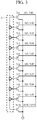
- FIG. 1 is a top view illustrating a pattern layout of a semiconductor device 1 according to a first embodiment of the present invention.
- FIG. 1 illustrates a multi-finger transistor which is the semiconductor device 1.
- FIG. 2 is a cross-sectional view illustrating a configuration of the semiconductor device 1 according to the first embodiment, and illustrates a cross section of the semiconductor device 1 taken along line A-A in FIG. 1 .
- the semiconductor device 1 includes gate fingers 2-1 to 2-6, drain electrodes 3-1 to 3-3, source electrodes 4-1 to 4-4, and a gate routing line 5.
- the gate fingers 2-1 to 2-6 are strip-shaped gate electrodes arranged in one direction.
- the gate finger 2-1 is disposed so as to be adjacent to the drain electrode 3-1 and the source electrode 4-1
- the gate finger 2-2 is disposed so as to be adjacent to the drain electrode 3-1 and the source electrode 4-2.
- the gate finger 2-3 is disposed so as to be adjacent to the drain electrode 3-2 and the source electrode 4-2, and the gate finger 2-4 is disposed so as to be adjacent to the drain electrode 3-2 and the source electrode 4-3.
- the gate finger 2-5 is disposed so as to be adjacent to the drain electrode 3-3 and the source electrode 4-3
- the gate finger 2-6 is disposed so as to be adjacent to the drain electrode 3-3 and the source electrode 4-4.
- each of the gate fingers 2-1 to 2-6 is disposed so as to be adjacent to the corresponding drain electrode and the corresponding source electrode alternately to form a comb-shaped electrode structure.
- the semiconductor device 1 illustrated in FIGS. 1 and 2 includes six transistor structures each including a gate finger, a drain electrode, and a source electrode.
- this transistor structure is referred to as a finger structure.
- the drain electrodes 3-1 to 3-3 are strip-shaped electrodes formed in a comb shape from a line 3a.
- the line 3a is a line extending in a direction in which the gate fingers 2-1 to 2-6 are arranged.
- the drain electrode 3-2 extends in a direction orthogonal to the line 3a, and an end portion thereof is an output point a.
- the drain electrode 3-2 is located at a center portion of the line 3a, and the multi-finger transistor which is the semiconductor device 1 is formed symmetrically with respect to the center portion as a boundary.
- the center portion is referred to as a transistor center portion, and both end portions are referred to as transistor end portions.
- the gate routing line 5 is a line extending in a direction in which the gate fingers 2-1 to 2-6 are arranged as surrounded by the broken line in FIG. 1 , and is connected to the individual gate fingers 2-1 to 2-6.
- a line 5a extending in the opposite direction to the gate fingers 2-1 to 2-6 is connected to a position corresponding to the transistor center portion in the gate routing line 5, and an end portion of the line 5a is an input point b.
- Power input to the input point b is distributed to the gate fingers 2-1 to 2-6 by the gate routing line 5.
- Each of the source electrodes 4-1 to 4-4 is a strip-shaped electrode disposed so as to be adjacent to the corresponding one or two of the gate fingers 2-1 to 2-6.
- a source pad 6-1 is an electrode pad disposed on one side with respect to the transistor center portion as a boundary so as to be adjacent to the line 5a.
- a source pad 6-2 is an electrode pad disposed on the other side with respect to the transistor center portion as a boundary so as to be adjacent to the line 5a.
- the source electrode 4-1 is connected to the source pad 6-1 by an air bridge 7-1
- the source electrode 4-2 is connected to the source pad 6-1 by an air bridge 7-2
- the source electrode 4-3 is connected to the source pad 6-2 by an air bridge 7-3
- the source electrode 4-4 is connected to the source pad 6-2 by an air bridge 7-4.
- the source pad 6-1 is electrically connected to a semiconductor layer 8 by a via hole 6a, and the source pad 6-2 is electrically connected to the semiconductor layer 8 by a via hole 6b.
- the gate fingers 2-1 to 2-3 are disposed on one side (left side in FIG. 2 ) with respect to the transistor center portion as a boundary, and the gate fingers 2-4 to 2-6 are disposed on the other side (right side in FIG. 2 ) with respect to the transistor center portion as a boundary.
- Each of the gate fingers 2-1 to 2-6 has a T-shaped gate head structure as illustrated in FIG. 2 .
- the gate finger 2-2 and the gate finger 2-5 each have a gate head length of GH1, and the gate finger 2-3 and the gate finger 2-4 each have a gate head length of GH2. Furthermore, the gate finger 2-1 and the gate finger 2-6 each have a gate head length of GH3. GH2 is longer than GH1, and GH3 is shorter than GH1.
- each of the gate fingers 2-1 and 2-6, the gate head length of each of the gate fingers 2-2 and 2-5, and the gate head length of each of the gate fingers 2-3 and 2-4 are different from one another and non-uniform.
- each of the gate fingers 2-1 to 2-6 has a longer gate head length as it is closer to the transistor center portion, and a shorter gate head length as it is closer to any one of the transistor end portions.
- the gate head length GH2 of the gate finger 2-3 adjacent to the transistor center portion is the longest
- the gate head length GH1 of the gate finger 2-2 adjacent thereto is the second longest
- the gate head length GH3 of the gate finger 2-1 at the transistor end portion is shorter than GH1.
- the finger structure at the transistor center portion includes the gate fingers 2-3 and 2-4 having long gate head lengths, and therefore has the largest gate-source capacitance Cgs and the largest gate-drain capacitance Cgd. Since each of the gate fingers has a shorter gate head length as it is closer to any one of the transistor end portions, the gate-source capacitance Cgs and the gate-drain capacitance Cgd in the corresponding finger structure gradually decrease. As a result, an imbalance in the input terminal impedances among the six respective finger structures is absorbed, and the input terminal impedances in all the finger structures are uniform.
- the RF drain currents output from the respective six finger structures also are uniform to reduce a difference between output terminal impedances in the respective finger structures. Therefore, deterioration in efficiency of the high frequency power amplifier using the semiconductor device 1 can be suppressed.
- the semiconductor device 1 can maintain the same gain as the conventional multi-finger transistor in which all the gate head lengths are GH1.
- FIG. 3 is a diagram illustrating a verification model of the semiconductor device according to the first embodiment.
- the finger transistor model Tri is a large signal equivalent circuit model modeling a finger structure having a gate finger length of 40 ⁇ m.
- a portion surrounded by the broken line corresponds to the gate routing line 5.
- ai is a coefficient representing the degree of non-uniformity of Cgs and Cgd due to non-uniformity of the gate head lengths.
- Cgd0 is a fixed value of the gate-drain capacitance.
- Cgs and Cgd in the finger transistor model Tri are non-uniform.
- the multi-finger transistor which is the semiconductor device 1 is referred to as a structure S2.
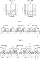
- FIG. 4 is a graph illustrating a relationship between each of ten finger transistor models Tri and an RF drain current Idi.
- the RF drain current Idi is a result of calculation using 28 GHz as a signal frequency, 20 mA as a bias drain current, 24 V as a bias drain voltage, a source impedance as a gain matching point, and a load impedance as an efficiency matching point in the verification models of the structures S1 and S2.
- a calculation result B1 of the RF drain current Idi was obtained by the verification model of the structure S1
- a calculation result B2 of the RF drain current Idi was obtained by the verification model of the structure S2.
- the conventional multi-finger transistor has an imbalance in the RF drain currents among the respective finger transistor models.
- the RF drain current Idi is substantially uniform in all the finger transistor models.
- FIG. 5A is a chart illustrating an output terminal impedance obtained by the verification model of the structure S1
- FIG. 5B is a chart illustrating an output terminal impedance obtained by the verification model of the structure S2.
- FIG. 6A is a graph illustrating drain efficiency obtained by the verification model of the structure S1.
- FIG. 6B is a graph illustrating drain efficiency obtained by the verification model of the structure S2.
- a peak value of drain efficiency ED (%) with respect to input power Pin obtained by the verification model of the structure S2 is about 2 points higher than that obtained by the verification model of the structure S1.
- the semiconductor device 1 includes the drain electrodes 3-1 to 3-3, the source electrodes 4-1 to 4-4, the gate fingers 2-1 to 2-6, and the gate routing line 5 disposed in a direction in which the fingers 2-1 to 2-6 are arranged, and connected to the individual gate fingers 2-1 to 2-6.
- the gate fingers 2-1 to 2-6 are arranged in one direction, each of the gate fingers is disposed so as to be adjacent to the corresponding one of the drain electrodes 3-1 to 3-3 and the corresponding one of the source electrodes 4-1 to 4-4 alternately, and the gate fingers have non-uniform gate head lengths.
- each of the gate fingers 2-1 to 2-6 has a longer gate head length as it is closer to the transistor center portion, and a shorter gate head length as it is closer to any one of the transistor end portions. In this way, by making the gate head lengths in the respective gate fingers 2-1 to 2-6 non-uniform, the RF drain currents can be uniform.
- FIG. 7 is a cross-sectional view illustrating a configuration of a semiconductor device 1A according to a second embodiment of the present invention, and illustrates a cross section of the semiconductor device 1A taken along line A-A in FIG. 1 .
- the same components as those in FIG. 2 are denoted by the same reference numerals, and description thereof is omitted.
- the gate head has a T-shape extending toward both the side of the corresponding drain electrode and the side of the corresponding source electrode.
- a gate head has a ⁇ shape extending only toward the side of a corresponding drain electrode. Even in the ⁇ -shaped gate head structure, by making the gate head lengths non-uniform, a balance of Cgs and Cgd in each of the plurality of finger structures can be changed.
- each of the gate fingers 2A-1 and 2A-6, the gate head length of each of the gate fingers 2A-2 and 2A-5, and the gate head length of each of the gate fingers 2A-3 and 2A-4 are different from one another and non-uniform.
- each of the gate fingers 2A-1 to 2A-6 has a longer gate head length as it is closer to the transistor center portion, and a shorter gate head length as it is closer to any one of the transistor end portions.
- a gate head length GH2 of the gate finger 2A-3 adjacent to the transistor center portion is the longest
- a gate head length GH1 of the gate finger 2A-2 adjacent thereto is the second longest
- a gate head length GH3 of the gate finger 2A-1 at the transistor end portion is shorter than GH1.
- the gate fingers 2A-4 to 2A-6 are constantly GH1
- the finger structure at the transistor center portion includes the gate fingers 2A-3 and 2A-4 having long gate head lengths, and therefore has the largest Cgs and Cgd. Since each of the gate fingers has a shorter gate head length as it is closer to any one of the transistor end portions, Cgs and Cgd in the corresponding finger structure gradually decrease. As a result, an imbalance in input terminal impedances among the six respective finger structures is absorbed, and the input terminal impedances in all the finger structures are uniform.
- the RF drain currents output from the respective six finger structures also are uniform to reduce a difference between output terminal impedances in the respective finger structures. Therefore, deterioration in efficiency of the high frequency power amplifier using the semiconductor device 1A can be suppressed.
- the semiconductor device 1A can maintain the same gain as the conventional multi-finger transistor in which the gate head length is GH1.
- each of the gate fingers 2A-1 to 2A-6 has a ⁇ -shaped gate head structure in which the shape of the gate head extends toward the side of the corresponding drain electrode.
- each of the gate fingers has a longer gate head length extending toward the side of the corresponding drain electrode as it is closer to the transistor center portion, and a shorter gate head length extending toward the side of the corresponding drain electrodes as it is closer to any one of the transistor end portions.
- the RF drain currents can be uniform.
- a difference between output terminal impedances in the respective gate fingers 2A-1 to 2A-6 is reduced, and therefore deterioration in efficiency of the high frequency power amplifier using the semiconductor device 1A can be suppressed.
- FIG. 8 is a cross-sectional view illustrating a configuration of a semiconductor device 1B according to a third embodiment of the present invention, and illustrates a cross section of the semiconductor device 1B taken along line A-A in FIG. 1 .
- the same components as those in FIG. 2 are denoted by the same reference numerals, and description thereof is omitted.
- the gate head lengths are non-uniform, but in the semiconductor device 1B according to the third embodiment, plate lengths of source field plates (hereinafter referred to as SFP) 9-1 to 9-6 are non-uniform. Even by making the plate lengths of the SFPs 9-1 to 9-6 non-uniform, a balance of Cgs and Cgd in each of the plurality of finger structures can be changed.
- SFP source field plates
- Gate fingers 2B-1 to 2B-6 are strip-shaped electrodes arranged in one direction, each of the gate fingers 2-1 to 2-6 is disposed so as to be adjacent to a corresponding drain electrode and a corresponding source electrode alternately, similarly to the gate fingers 2-1 to 2-6 described in the first embodiment. Note that the gate head lengths of the gate fingers 2B-1 to 2B-6 are all GH1.
- each of source electrodes 4A-1 to 4A-4 is a strip-shaped electrode disposed so as to be adjacent to the corresponding one or two of the gate fingers 2B-1 to 2B-6.
- Each of the SFPs 9-1 to 9-6 is a member that is provided for the corresponding one of the source electrodes 4A-1 to 4A-4 and extends from the corresponding one of the source electrodes 4A-1 to 4A-4 toward the corresponding one of the sides of the gate fingers 2B-1 to 2B-6.
- the source electrode 4A-1 has the SFP 9-1 extending toward the side of the gate finger 2B-1.
- the source electrode 4A-2 has the SFP 9-2 extending toward the side of the gate finger 2B-2 and the SFP 9-3 extending toward the side of the gate finger 2B-3.
- the source electrode 4A-3 has the SFP 9-4 extending toward the side of the gate finger 2B-4 and the SFP 9-5 extending toward the side of the gate finger 2B-5.
- the source electrode 4A-4 has the SFP 9-6 extending toward the side of the gate finger 2B-6.
- the plate lengths of the SFP 9-3 and SFP 9-4 adjacent to the transistor center portion are the longest, and the plate lengths of the SFP 9-2 and SFP 9-5 adjacent thereto are the second longest, and the plate lengths of the SFP9-1 and SFP9-6 at the respective transistor end portions are the shortest.
- the finger structure at the transistor center portion includes the SFPs 9-3 and 9-4 having long plate lengths, and therefore has the largest Cgs and Cgd. Since each of the SFPs has a shorter plate length as it is closer to any one of the transistor end portions, Cgs and Cgd in the corresponding finger structure gradually decrease. As a result, an imbalance in input terminal impedances among the six respective finger structures is absorbed, and the input terminal impedances in all the finger structures are uniform.
- the RF drain currents output from the six respective finger structures also are uniform to reduce a difference between output terminal impedances in the respective finger structures. Therefore, deterioration in efficiency of the high frequency power amplifier using the semiconductor device 1B can be suppressed.
- the semiconductor device 1B includes the SFPs 9-1 to 9-6 each of which is provided for the corresponding one of the source electrodes 4A-1 to 4A-4 and extends from the corresponding one of the source electrodes 4A-1 to 4A-4 toward the corresponding one of the sides of the gate fingers 2B-1 to 2B-6.
- each of the SFPs 9-1 to 9-6 has a longer plate length as it is closer to the transistor center portion, and a shorter plate length as it is closer to any one of the transistor end portions. In this way, by making the plate lengths of the SFPs 9-1 to 9-6 non-uniform, the RF drain currents can be uniform. As a result, a difference between output terminal impedances in the plurality of respective finger structures is reduced, and therefore deterioration in efficiency of the high frequency power amplifier using the semiconductor device 1B can be suppressed.
- the semiconductor device according to the present invention can suppress deterioration in efficiency by reducing a difference between output terminal impedances in the plurality of respective gate electrodes, and therefore can be used for a high frequency power amplifier.
- 1, 1A, 1B Semiconductor device, 2-1 to 2-6, 2A-1 to 2A-6, 2B-1 to 2B-6: Gate finger, 3-1 to 3-3: Drain electrode, 3a, 5a: Line, 4-1 to 4-4, 4A-1 to 4A-4: Source electrode, 5: Gate routing line, 6-1, 6-2: Source pad, 6a, 6b: Via hole, 7-1 to 7-4: Air bridge, 8: Semiconductor layer, 9-1 to 9-6: Source field plate (SFP).
- SFP Source field plate
Landscapes
- Junction Field-Effect Transistors (AREA)
- Electrodes Of Semiconductors (AREA)
Abstract
Description
- The present invention relates to a semiconductor device, for example, used for a high frequency power amplifier, such as a field effect transistor.
- A multi-finger transistor includes a plurality of strip-shaped source electrodes, a plurality of strip-shaped gate electrodes, and a plurality of strip-shaped drain electrodes, and the source electrodes, the gate electrodes, and the drain electrodes are alternately arranged (see, for example, Patent Literature 1). The multi-finger transistor also includes a gate routing line extending from one end portion of the transistor through a center portion thereof to the other end portion. By supplying power to an input point at a center portion of the gate routing line, power is distributed to each of the plurality of gate electrodes by the gate routing line.
- Patent Literature 1:
JP 2011-204984 A - In the multi-finger transistor described in
Patent Literature 1, there is a difference between a distance from a gate electrode disposed adjacent to a center portion of the transistor to an input point and a distance from a gate electrode disposed at an end portion of the transistor to the input point. For this reason, power input to a plurality of gate electrodes by a gate routing line is unbalanced. - If the power input to the plurality of gate electrodes is unbalanced, an RF drain current is high at a center portion of the transistor and low at an end portion of the transistor. As a result, a difference between output terminal impedances occurs in the respective plurality of transistor structures each including a source electrode, a gate electrode, and a drain electrode, and efficiency of an amplifier using the multi-finger transistor is deteriorated disadvantageously.
- The present invention solves the above disadvantage, and an object of the present invention is to obtain a semiconductor device capable of reducing a variation in output terminal impedances.
- A semiconductor device according to the present invention includes: a plurality of drain electrodes; a plurality of source electrodes, a plurality of gate electrodes that are arranged in one direction and each of which is disposed so as to be adjacent to a corresponding one of the drain electrodes and a corresponding one of the source electrodes alternately; and a gate routing line disposed in the direction in which the gate electrodes are arranged, and connected to the plurality of gate electrodes. In this configuration, the plurality of gate electrodes is arranged in the one direction, each of the gate electrodes is disposed so as to be adjacent to the corresponding one of the drain electrodes and the corresponding one of the source electrodes alternately, and the gate electrodes have non-uniform gate head lengths.
- According to the present invention, by making the gate head lengths of the plurality of gate electrodes non-uniform, it is possible to make RF drain currents uniform and to reduce a variation in output terminal impedances.
-
-
FIG. 1 is a top view illustrating a pattern layout of a semiconductor device according to a first embodiment of the present invention. -
FIG. 2 is a cross-sectional view illustrating a configuration of the semiconductor device according to the first embodiment. -
FIG. 3 is a diagram illustrating a verification model of the semiconductor device according to the first embodiment. -
FIG. 4 is a graph illustrating a relationship between each of ten finger transistor models and an RF drain current. -
FIG. 5A is a chart illustrating an output terminal impedance of a conventional semiconductor device.FIG. 5B is a chart illustrating an output terminal impedance of the semiconductor device according to the first embodiment. -
FIG. 6A is a graph illustrating drain efficiency of the conventional semiconductor device.FIG. 6B is a graph illustrating drain efficiency of the semiconductor device according to the first embodiment. -
FIG. 7 is a cross-sectional view illustrating a configuration of a semiconductor device according to a second embodiment of the present invention. -
FIG. 8 is a cross-sectional view illustrating a configuration of a semiconductor device according to a third embodiment of the present invention. - Hereinafter, in order to describe the present invention in more detail, embodiments for carrying out the present invention will be described with reference to the attached drawings.
-
FIG. 1 is a top view illustrating a pattern layout of asemiconductor device 1 according to a first embodiment of the present invention.FIG. 1 illustrates a multi-finger transistor which is thesemiconductor device 1.FIG. 2 is a cross-sectional view illustrating a configuration of thesemiconductor device 1 according to the first embodiment, and illustrates a cross section of thesemiconductor device 1 taken along line A-A inFIG. 1 . As illustrated inFIG. 1 , thesemiconductor device 1 includes gate fingers 2-1 to 2-6, drain electrodes 3-1 to 3-3, source electrodes 4-1 to 4-4, and agate routing line 5. The gate fingers 2-1 to 2-6 are strip-shaped gate electrodes arranged in one direction. - The gate finger 2-1 is disposed so as to be adjacent to the drain electrode 3-1 and the source electrode 4-1, and the gate finger 2-2 is disposed so as to be adjacent to the drain electrode 3-1 and the source electrode 4-2. The gate finger 2-3 is disposed so as to be adjacent to the drain electrode 3-2 and the source electrode 4-2, and the gate finger 2-4 is disposed so as to be adjacent to the drain electrode 3-2 and the source electrode 4-3. The gate finger 2-5 is disposed so as to be adjacent to the drain electrode 3-3 and the source electrode 4-3, and the gate finger 2-6 is disposed so as to be adjacent to the drain electrode 3-3 and the source electrode 4-4.
- As described above, each of the gate fingers 2-1 to 2-6 is disposed so as to be adjacent to the corresponding drain electrode and the corresponding source electrode alternately to form a comb-shaped electrode structure.
- Note that the
semiconductor device 1 illustrated inFIGS. 1 and 2 includes six transistor structures each including a gate finger, a drain electrode, and a source electrode. - Hereinafter, this transistor structure is referred to as a finger structure.
- The drain electrodes 3-1 to 3-3 are strip-shaped electrodes formed in a comb shape from a
line 3a. Theline 3a is a line extending in a direction in which the gate fingers 2-1 to 2-6 are arranged. The drain electrode 3-2 extends in a direction orthogonal to theline 3a, and an end portion thereof is an output point a. As illustrated inFIG. 1 , the drain electrode 3-2 is located at a center portion of theline 3a, and the multi-finger transistor which is thesemiconductor device 1 is formed symmetrically with respect to the center portion as a boundary. Hereinafter, the center portion is referred to as a transistor center portion, and both end portions are referred to as transistor end portions. - The
gate routing line 5 is a line extending in a direction in which the gate fingers 2-1 to 2-6 are arranged as surrounded by the broken line inFIG. 1 , and is connected to the individual gate fingers 2-1 to 2-6. Aline 5a extending in the opposite direction to the gate fingers 2-1 to 2-6 is connected to a position corresponding to the transistor center portion in thegate routing line 5, and an end portion of theline 5a is an input point b. - Power input to the input point b is distributed to the gate fingers 2-1 to 2-6 by the
gate routing line 5. - Each of the source electrodes 4-1 to 4-4 is a strip-shaped electrode disposed so as to be adjacent to the corresponding one or two of the gate fingers 2-1 to 2-6.
- A source pad 6-1 is an electrode pad disposed on one side with respect to the transistor center portion as a boundary so as to be adjacent to the
line 5a. A source pad 6-2 is an electrode pad disposed on the other side with respect to the transistor center portion as a boundary so as to be adjacent to theline 5a. - The source electrode 4-1 is connected to the source pad 6-1 by an air bridge 7-1, and the source electrode 4-2 is connected to the source pad 6-1 by an air bridge 7-2. The source electrode 4-3 is connected to the source pad 6-2 by an air bridge 7-3, and the source electrode 4-4 is connected to the source pad 6-2 by an air bridge 7-4.
- The source pad 6-1 is electrically connected to a
semiconductor layer 8 by avia hole 6a, and the source pad 6-2 is electrically connected to thesemiconductor layer 8 by avia hole 6b. - The gate fingers 2-1 to 2-3 are disposed on one side (left side in
FIG. 2 ) with respect to the transistor center portion as a boundary, and the gate fingers 2-4 to 2-6 are disposed on the other side (right side inFIG. 2 ) with respect to the transistor center portion as a boundary. Each of the gate fingers 2-1 to 2-6 has a T-shaped gate head structure as illustrated inFIG. 2 . - The gate finger 2-2 and the gate finger 2-5 each have a gate head length of GH1, and the gate finger 2-3 and the gate finger 2-4 each have a gate head length of GH2. Furthermore, the gate finger 2-1 and the gate finger 2-6 each have a gate head length of GH3. GH2 is longer than GH1, and GH3 is shorter than GH1.
- In a conventional multi-finger transistor, all of the gate fingers 2-1 to 2-6 illustrated in
FIGS. 1 and 2 have the same gate head length. Therefore, unbalanced power input to each of the gate fingers 2-1 to 2-6 by thegate routing line 5 is amplified as it is, and thus RF drain currents are unbalanced in a direction indicated by the broken line arrow inFIG. 1 . - In this way, when the RF drain currents are unbalanced among the six respective finger structures, a difference between output terminal impedances in the six respective finger structures is also generated.
- As a result, a difference between an output terminal impedance of a finger structure and an optimum impedance with maximum efficiency of the transistor is large, and therefore, for example, efficiency of a high frequency power amplifier using a multi-finger transistor is deteriorated.
- Meanwhile, in the
semiconductor device 1, the gate head length of each of the gate fingers 2-1 and 2-6, the gate head length of each of the gate fingers 2-2 and 2-5, and the gate head length of each of the gate fingers 2-3 and 2-4 are different from one another and non-uniform. In particular, each of the gate fingers 2-1 to 2-6 has a longer gate head length as it is closer to the transistor center portion, and a shorter gate head length as it is closer to any one of the transistor end portions. - In
FIG. 2 , the gate head length GH2 of the gate finger 2-3 adjacent to the transistor center portion is the longest, the gate head length GH1 of the gate finger 2-2 adjacent thereto is the second longest, and the gate head length GH3 of the gate finger 2-1 at the transistor end portion is shorter than GH1. The same applies to the gate fingers 2-4 to 2-6. - When all the gate head lengths of the conventional multi-finger transistor are constantly GH1, in the
semiconductor device 1, an average value of the gate head lengths of the gate fingers 2-1 to 2-6 is set to GH1. That is, the average value of the gate head lengths is (GH1 + GH2 + GH3) × 2/6 = GH1. - The finger structure at the transistor center portion includes the gate fingers 2-3 and 2-4 having long gate head lengths, and therefore has the largest gate-source capacitance Cgs and the largest gate-drain capacitance Cgd. Since each of the gate fingers has a shorter gate head length as it is closer to any one of the transistor end portions, the gate-source capacitance Cgs and the gate-drain capacitance Cgd in the corresponding finger structure gradually decrease. As a result, an imbalance in the input terminal impedances among the six respective finger structures is absorbed, and the input terminal impedances in all the finger structures are uniform.
- When the input terminal impedances are uniform, the RF drain currents output from the respective six finger structures also are uniform to reduce a difference between output terminal impedances in the respective finger structures. Therefore, deterioration in efficiency of the high frequency power amplifier using the
semiconductor device 1 can be suppressed. - In addition, when the average value of the gate head lengths of the gate fingers 2-1 to 2-6 is GH1, the
semiconductor device 1 can maintain the same gain as the conventional multi-finger transistor in which all the gate head lengths are GH1. - The above effect of the
semiconductor device 1 was verified using a commercially available microwave circuit simulator. -
FIG. 3 is a diagram illustrating a verification model of the semiconductor device according to the first embodiment. The verification model illustrated inFIG. 3 models a multi-finger transistor structure by combining 10 finger transistor models Tri (i = 1 to 10) with a line component model prepared in the microwave circuit simulator. The finger transistor model Tri is a large signal equivalent circuit model modeling a finger structure having a gate finger length of 40 µm. In the verification model, a portion surrounded by the broken line corresponds to thegate routing line 5. - An RF drain current output from a transistor of the finger transistor model Tri is represented by Idi (i = 1 to 10), and an RF drain voltage is represented by Vdi (i = 1 to 10).
- In the finger transistor model Tri, a gate-source capacitance Cgsi (i = 1 to 10) is defined as ai × Cgsi, and a gate-drain capacitance Cgdi (i = 1 to 10) is defined as ai × Cgd0. ai is a coefficient representing the degree of non-uniformity of Cgs and Cgd due to non-uniformity of the gate head lengths. Cgd0 is a fixed value of the gate-drain capacitance.
- In the conventional multi-finger transistor, a1 = a2 = a3 =... = a10 = 1, and the gate head lengths of all the finger transistor models Tri are uniform.
- Hereinafter, the conventional multi-finger transistor in which ai = 1 is referred to as a structure S1.
- In the multi-finger transistor which is the
semiconductor device 1, a1 = 0.9, a2 = 0.95, a3 = 1, a4 = 1.05, a5 = 1.1, a6 = 1.1, a7 = 1.05, a8 = 1, a9 = 1.05, and a10 = 1.1. As a result, Cgs and Cgd in the finger transistor model Tri are non-uniform. - Hereinafter, the multi-finger transistor which is the
semiconductor device 1 is referred to as a structure S2. -
FIG. 4 is a graph illustrating a relationship between each of ten finger transistor models Tri and an RF drain current Idi. InFIG. 4 , the RF drain current Idi is a result of calculation using 28 GHz as a signal frequency, 20 mA as a bias drain current, 24 V as a bias drain voltage, a source impedance as a gain matching point, and a load impedance as an efficiency matching point in the verification models of the structures S1 and S2. A calculation result B1 of the RF drain current Idi was obtained by the verification model of the structure S1, and a calculation result B2 of the RF drain current Idi was obtained by the verification model of the structure S2. - In the calculation result B1 of the RF drain current Idi, the RF drain current Idi of the finger transistor model Tri (i = 5, 6) at the transistor center portion is low. The RF drain current Idi of the finger transistor model Tri (i = 1, 10) at each of the transistor end portions is high.
- In this way, the conventional multi-finger transistor has an imbalance in the RF drain currents among the respective finger transistor models.
- Meanwhile, in the calculation result B2 of the RF drain current Idi, as illustrated in
FIG. 4 , the RF drain current Idi is substantially uniform in all the finger transistor models. - That is, in the multi-finger transistor which is the
semiconductor device 1, an imbalance in RF drain currents among the respective finger transistor models is alleviated. -
FIG. 5A is a chart illustrating an output terminal impedance obtained by the verification model of the structure S1, andFIG. 5B is a chart illustrating an output terminal impedance obtained by the verification model of the structure S2. InFIGS. 5A and 5B , the output terminal impedance is Vdi/Idi (i = 1 to 10). In the conventional multi-finger transistor, as illustrated in the enlarged chart inFIG. 5A , the values of Vdi/Idi (i = 1 to 10) do not converge to one, and there is a variation. In the multi-finger transistor which is thesemiconductor device 1, as illustrated in the enlarged chart inFIG. 5B , the values of Vdi/Idi (i = 1 to 10) converge to one. -
FIG. 6A is a graph illustrating drain efficiency obtained by the verification model of the structure S1.FIG. 6B is a graph illustrating drain efficiency obtained by the verification model of the structure S2. - In
FIGS. 6A and 6B , a peak value of drain efficiency ED (%) with respect to input power Pin obtained by the verification model of the structure S2 is about 2 points higher than that obtained by the verification model of the structure S1. - As described above, the
semiconductor device 1 according to the first embodiment includes the drain electrodes 3-1 to 3-3, the source electrodes 4-1 to 4-4, the gate fingers 2-1 to 2-6, and thegate routing line 5 disposed in a direction in which the fingers 2-1 to 2-6 are arranged, and connected to the individual gate fingers 2-1 to 2-6. - In this configuration, the gate fingers 2-1 to 2-6 are arranged in one direction, each of the gate fingers is disposed so as to be adjacent to the corresponding one of the drain electrodes 3-1 to 3-3 and the corresponding one of the source electrodes 4-1 to 4-4 alternately, and the gate fingers have non-uniform gate head lengths. In particular, each of the gate fingers 2-1 to 2-6 has a longer gate head length as it is closer to the transistor center portion, and a shorter gate head length as it is closer to any one of the transistor end portions. In this way, by making the gate head lengths in the respective gate fingers 2-1 to 2-6 non-uniform, the RF drain currents can be uniform.
- As a result, a difference between output terminal impedances in the plurality of respective finger structures is reduced, and therefore deterioration in efficiency of the high frequency power amplifier using the
semiconductor device 1 can be suppressed. -
FIG. 7 is a cross-sectional view illustrating a configuration of a semiconductor device 1A according to a second embodiment of the present invention, and illustrates a cross section of the semiconductor device 1A taken along line A-A inFIG. 1 . InFIG. 7 , the same components as those inFIG. 2 are denoted by the same reference numerals, and description thereof is omitted. - In the
semiconductor device 1 according to the first embodiment, the gate head has a T-shape extending toward both the side of the corresponding drain electrode and the side of the corresponding source electrode. However, in the semiconductor device 1A according to the second embodiment, a gate head has a Γ shape extending only toward the side of a corresponding drain electrode. Even in the Γ-shaped gate head structure, by making the gate head lengths non-uniform, a balance of Cgs and Cgd in each of the plurality of finger structures can be changed. - In the semiconductor device 1A, the gate head length of each of the
gate fingers 2A-1 and 2A-6, the gate head length of each of thegate fingers 2A-2 and 2A-5, and the gate head length of each of thegate fingers 2A-3 and 2A-4 are different from one another and non-uniform. In particular, each of thegate fingers 2A-1 to 2A-6 has a longer gate head length as it is closer to the transistor center portion, and a shorter gate head length as it is closer to any one of the transistor end portions. - As illustrated in
FIG. 7 , a gate head length GH2 of thegate finger 2A-3 adjacent to the transistor center portion is the longest, a gate head length GH1 of thegate finger 2A-2 adjacent thereto is the second longest, and a gate head length GH3 of thegate finger 2A-1 at the transistor end portion is shorter than GH1. The same applies to thegate fingers 2A-4 to 2A-6. When all the gate head lengths of the conventional multi-finger transistor are constantly GH1, in the semiconductor device 1A, an average value of the gate head lengths of thegate fingers 2A-1 to 2A-6 is set to GH1. That is, the average value of the gate head lengths is (GH1 + GH2 + GH3) × 2/6 = GH1. - The finger structure at the transistor center portion includes the
gate fingers 2A-3 and 2A-4 having long gate head lengths, and therefore has the largest Cgs and Cgd. Since each of the gate fingers has a shorter gate head length as it is closer to any one of the transistor end portions, Cgs and Cgd in the corresponding finger structure gradually decrease. As a result, an imbalance in input terminal impedances among the six respective finger structures is absorbed, and the input terminal impedances in all the finger structures are uniform. - When the input terminal impedances are uniform, the RF drain currents output from the respective six finger structures also are uniform to reduce a difference between output terminal impedances in the respective finger structures. Therefore, deterioration in efficiency of the high frequency power amplifier using the semiconductor device 1A can be suppressed.
- In addition, when the average value of the gate head lengths of the
gate fingers 2A-1 to 2A-6 is GH1, the semiconductor device 1A can maintain the same gain as the conventional multi-finger transistor in which the gate head length is GH1. - As described above, in the semiconductor device 1A according to the second embodiment, each of the
gate fingers 2A-1 to 2A-6 has a Γ-shaped gate head structure in which the shape of the gate head extends toward the side of the corresponding drain electrode. In this configuration, each of the gate fingers has a longer gate head length extending toward the side of the corresponding drain electrode as it is closer to the transistor center portion, and a shorter gate head length extending toward the side of the corresponding drain electrodes as it is closer to any one of the transistor end portions. In this way, by making the gate head lengths in thegate fingers 2A-1 to 2A-6 non-uniform, the RF drain currents can be uniform. As a result, a difference between output terminal impedances in therespective gate fingers 2A-1 to 2A-6 is reduced, and therefore deterioration in efficiency of the high frequency power amplifier using the semiconductor device 1A can be suppressed. -
FIG. 8 is a cross-sectional view illustrating a configuration of asemiconductor device 1B according to a third embodiment of the present invention, and illustrates a cross section of thesemiconductor device 1B taken along line A-A inFIG. 1 . InFIG. 8 , the same components as those inFIG. 2 are denoted by the same reference numerals, and description thereof is omitted. - In the
semiconductor device 1 according to the first embodiment and the semiconductor device 1A according to the second embodiment, the gate head lengths are non-uniform, but in thesemiconductor device 1B according to the third embodiment, plate lengths of source field plates (hereinafter referred to as SFP) 9-1 to 9-6 are non-uniform. Even by making the plate lengths of the SFPs 9-1 to 9-6 non-uniform, a balance of Cgs and Cgd in each of the plurality of finger structures can be changed. -
Gate fingers 2B-1 to 2B-6 are strip-shaped electrodes arranged in one direction, each of the gate fingers 2-1 to 2-6 is disposed so as to be adjacent to a corresponding drain electrode and a corresponding source electrode alternately, similarly to the gate fingers 2-1 to 2-6 described in the first embodiment. Note that the gate head lengths of thegate fingers 2B-1 to 2B-6 are all GH1. - In
FIG. 8 , each ofsource electrodes 4A-1 to 4A-4 is a strip-shaped electrode disposed so as to be adjacent to the corresponding one or two of thegate fingers 2B-1 to 2B-6. Each of the SFPs 9-1 to 9-6 is a member that is provided for the corresponding one of thesource electrodes 4A-1 to 4A-4 and extends from the corresponding one of thesource electrodes 4A-1 to 4A-4 toward the corresponding one of the sides of thegate fingers 2B-1 to 2B-6. - The
source electrode 4A-1 has the SFP 9-1 extending toward the side of thegate finger 2B-1. Thesource electrode 4A-2 has the SFP 9-2 extending toward the side of thegate finger 2B-2 and the SFP 9-3 extending toward the side of thegate finger 2B-3. Thesource electrode 4A-3 has the SFP 9-4 extending toward the side of thegate finger 2B-4 and the SFP 9-5 extending toward the side of thegate finger 2B-5. Thesource electrode 4A-4 has the SFP 9-6 extending toward the side of thegate finger 2B-6. - As illustrated in
FIG. 8 , the plate lengths of the SFP 9-3 and SFP 9-4 adjacent to the transistor center portion are the longest, and the plate lengths of the SFP 9-2 and SFP 9-5 adjacent thereto are the second longest, and the plate lengths of the SFP9-1 and SFP9-6 at the respective transistor end portions are the shortest. - The finger structure at the transistor center portion includes the SFPs 9-3 and 9-4 having long plate lengths, and therefore has the largest Cgs and Cgd. Since each of the SFPs has a shorter plate length as it is closer to any one of the transistor end portions, Cgs and Cgd in the corresponding finger structure gradually decrease. As a result, an imbalance in input terminal impedances among the six respective finger structures is absorbed, and the input terminal impedances in all the finger structures are uniform.
- When the input terminal impedances are uniform, the RF drain currents output from the six respective finger structures also are uniform to reduce a difference between output terminal impedances in the respective finger structures. Therefore, deterioration in efficiency of the high frequency power amplifier using the
semiconductor device 1B can be suppressed. - As described above, the
semiconductor device 1B according to the third embodiment includes the SFPs 9-1 to 9-6 each of which is provided for the corresponding one of thesource electrodes 4A-1 to 4A-4 and extends from the corresponding one of thesource electrodes 4A-1 to 4A-4 toward the corresponding one of the sides of thegate fingers 2B-1 to 2B-6. In particular, each of the SFPs 9-1 to 9-6 has a longer plate length as it is closer to the transistor center portion, and a shorter plate length as it is closer to any one of the transistor end portions. In this way, by making the plate lengths of the SFPs 9-1 to 9-6 non-uniform, the RF drain currents can be uniform. As a result, a difference between output terminal impedances in the plurality of respective finger structures is reduced, and therefore deterioration in efficiency of the high frequency power amplifier using thesemiconductor device 1B can be suppressed. - Note that in the present invention, it is possible to freely combine the embodiments to each other, modify any constituent element in each of the embodiments, or omit any constituent element in each of the embodiments within the scope of the invention.
- The semiconductor device according to the present invention can suppress deterioration in efficiency by reducing a difference between output terminal impedances in the plurality of respective gate electrodes, and therefore can be used for a high frequency power amplifier.
- 1, 1A, 1B: Semiconductor device, 2-1 to 2-6, 2A-1 to 2A-6, 2B-1 to 2B-6: Gate finger, 3-1 to 3-3: Drain electrode, 3a, 5a: Line, 4-1 to 4-4, 4A-1 to 4A-4: Source electrode, 5: Gate routing line, 6-1, 6-2: Source pad, 6a, 6b: Via hole, 7-1 to 7-4: Air bridge, 8: Semiconductor layer, 9-1 to 9-6: Source field plate (SFP).
Claims (5)
- A semiconductor device comprising:a plurality of drain electrodes;a plurality of source electrodes;a plurality of gate electrodes that are arranged in one direction and each of which is disposed so as to be adjacent to a corresponding one of the drain electrodes and a corresponding one of the source electrodes alternately; anda gate routing line disposed in the direction in which the gate electrodes are arranged, and connected to the plurality of gate electrodes, whereinthe plurality of gate electrodes has non-uniform gate head lengths.
- The semiconductor device according to claim 1, wherein
each of the plurality of gate electrodes has a longer gate head length as it is closer to a transistor center portion, and a shorter gate head length as it is closer to any one of transistor end portions. - The semiconductor device according to claim 1, wherein
each of the plurality of gate electrodes has a Γ-shaped gate head structure in which a gate head shape extends toward a side of the corresponding one of the drain electrodes. - The semiconductor device according to claim 3, wherein
each of the plurality of gate electrodes has a longer gate head length extending toward the side of the corresponding one of the drain electrodes as it is closer to a transistor center portion, and a shorter gate head length extending to the side of the corresponding one of the drain electrodes as it is closer to any one of transistor end portions. - A semiconductor device comprising:a plurality of drain electrodes;a plurality of source electrodes;a plurality of gate electrodes that are arranged in one direction and each of which is disposed so as to be adjacent to a corresponding one of the drain electrodes and a corresponding one of the source electrodes alternately;a gate routing line disposed in the direction in which the gate electrodes are arranged, and connected to the plurality of gate electrodes; anda plurality of source field plates each of which is provided for a corresponding one of the plurality of source electrodes and each of which extends from the corresponding one of the source electrodes toward a side of a corresponding one of the gate electrodes, whereineach of the plurality of source field plates has a longer plate length as it is closer to a transistor center portion, and a shorter plate length as it is closer to any one of transistor end portions.
Applications Claiming Priority (1)
| Application Number | Priority Date | Filing Date | Title |
|---|---|---|---|
| PCT/JP2017/018676 WO2018211661A1 (en) | 2017-05-18 | 2017-05-18 | Semiconductor device |
Publications (3)
| Publication Number | Publication Date |
|---|---|
| EP3618100A1 true EP3618100A1 (en) | 2020-03-04 |
| EP3618100A4 EP3618100A4 (en) | 2020-07-22 |
| EP3618100B1 EP3618100B1 (en) | 2021-08-18 |
Family
ID=64273639
Family Applications (1)
| Application Number | Title | Priority Date | Filing Date |
|---|---|---|---|
| EP17909764.7A Active EP3618100B1 (en) | 2017-05-18 | 2017-05-18 | Semiconductor device |
Country Status (4)
| Country | Link |
|---|---|
| US (1) | US10741700B2 (en) |
| EP (1) | EP3618100B1 (en) |
| JP (1) | JP6647454B2 (en) |
| WO (1) | WO2018211661A1 (en) |
Families Citing this family (1)
| Publication number | Priority date | Publication date | Assignee | Title |
|---|---|---|---|---|
| JP2023049404A (en) * | 2021-09-29 | 2023-04-10 | 住友電工デバイス・イノベーション株式会社 | Semiconductor device |
Family Cites Families (12)
| Publication number | Priority date | Publication date | Assignee | Title |
|---|---|---|---|---|
| JPH06151471A (en) | 1992-11-09 | 1994-05-31 | Fujitsu Ltd | Structure of field effect transistor |
| JPH0845961A (en) | 1994-08-04 | 1996-02-16 | Nec Corp | Field effect transistor |
| JP2757848B2 (en) * | 1996-01-23 | 1998-05-25 | 日本電気株式会社 | Field effect type semiconductor device |
| US6023086A (en) * | 1997-09-02 | 2000-02-08 | Motorola, Inc. | Semiconductor transistor with stabilizing gate electrode |
| JP2006032522A (en) * | 2004-07-14 | 2006-02-02 | Alps Electric Co Ltd | Exchange coupling film and magnetic sensing element using the exchange coupling film |
| JP2006032552A (en) * | 2004-07-14 | 2006-02-02 | Toshiba Corp | Nitride-containing semiconductor device |
| US8203185B2 (en) * | 2005-06-21 | 2012-06-19 | Cree, Inc. | Semiconductor devices having varying electrode widths to provide non-uniform gate pitches and related methods |
| JP5658472B2 (en) | 2010-03-26 | 2015-01-28 | ルネサスエレクトロニクス株式会社 | Field effect transistor |
| JP6025295B2 (en) * | 2010-06-24 | 2016-11-16 | 富士通株式会社 | Compound semiconductor device |
| JP6022804B2 (en) * | 2011-07-25 | 2016-11-09 | ルネサスエレクトロニクス株式会社 | Semiconductor integrated circuit |
| JP2013110269A (en) * | 2011-11-21 | 2013-06-06 | Samsung Electro-Mechanics Co Ltd | Cmos integrated circuit and amplifier circuit |
| US10199470B2 (en) * | 2016-11-08 | 2019-02-05 | Raytheon Company | Field effect transistor having staggered field effect transistor cells |
-
2017
- 2017-05-18 EP EP17909764.7A patent/EP3618100B1/en active Active
- 2017-05-18 JP JP2019518698A patent/JP6647454B2/en active Active
- 2017-05-18 US US16/604,092 patent/US10741700B2/en active Active
- 2017-05-18 WO PCT/JP2017/018676 patent/WO2018211661A1/en not_active Ceased
Also Published As
| Publication number | Publication date |
|---|---|
| US20200152803A1 (en) | 2020-05-14 |
| US10741700B2 (en) | 2020-08-11 |
| WO2018211661A1 (en) | 2018-11-22 |
| JP6647454B2 (en) | 2020-02-14 |
| EP3618100B1 (en) | 2021-08-18 |
| JPWO2018211661A1 (en) | 2019-11-07 |
| EP3618100A4 (en) | 2020-07-22 |
Similar Documents
| Publication | Publication Date | Title |
|---|---|---|
| US10170400B2 (en) | Multi-finger transistor and semiconductor device | |
| JPWO2010113779A1 (en) | Semiconductor device | |
| JPWO2015033490A1 (en) | Semiconductor device | |
| CN106464137A (en) | Switching converter and electronic device using same | |
| JP6319509B2 (en) | Semiconductor device | |
| US10256224B2 (en) | Multiple-unit semiconductor device | |
| JP7113381B2 (en) | switching circuit | |
| EP3305018A1 (en) | Power supply apparatus for induction heating | |
| EP3872844A1 (en) | Semiconductor device | |
| KR20180034205A (en) | Semiconductor device | |
| EP3618100B1 (en) | Semiconductor device | |
| CN103180938A (en) | Capacitor array and signal processing device with the capacitor array | |
| US20200118950A1 (en) | Amplifier | |
| CN108766999B (en) | Terminal for semiconductor power device | |
| CN110120746B (en) | A multi-phase parallel DCDC circuit and its chip structure | |
| US20230307517A1 (en) | Transistor | |
| CN108550567A (en) | A kind of integrated cellular gate resistance layout design of power semiconductor chip | |
| US10700681B1 (en) | Paralleled power module with additional emitter/source path | |
| EP4113575A1 (en) | Variable inductor for plasma generator | |
| CN106233598A (en) | Supply unit | |
| JPH06310955A (en) | High output field effect transistor | |
| US10777550B2 (en) | Semiconductor device | |
| JPWO2018138764A1 (en) | Transistor | |
| JP5398841B2 (en) | Power amplifier | |
| US20190356309A1 (en) | Switch circuit |
Legal Events
| Date | Code | Title | Description |
|---|---|---|---|
| STAA | Information on the status of an ep patent application or granted ep patent |
Free format text: STATUS: THE INTERNATIONAL PUBLICATION HAS BEEN MADE |
|
| PUAI | Public reference made under article 153(3) epc to a published international application that has entered the european phase |
Free format text: ORIGINAL CODE: 0009012 |
|
| STAA | Information on the status of an ep patent application or granted ep patent |
Free format text: STATUS: REQUEST FOR EXAMINATION WAS MADE |
|
| 17P | Request for examination filed |
Effective date: 20191113 |
|
| AK | Designated contracting states |
Kind code of ref document: A1 Designated state(s): AL AT BE BG CH CY CZ DE DK EE ES FI FR GB GR HR HU IE IS IT LI LT LU LV MC MK MT NL NO PL PT RO RS SE SI SK SM TR |
|
| AX | Request for extension of the european patent |
Extension state: BA ME |
|
| RIC1 | Information provided on ipc code assigned before grant |
Ipc: H01L 29/40 20060101ALI20200310BHEP Ipc: H01L 29/423 20060101ALI20200310BHEP Ipc: H01L 29/417 20060101AFI20200310BHEP |
|
| REG | Reference to a national code |
Ref country code: DE Ref legal event code: R079 Ref document number: 602017044525 Country of ref document: DE Free format text: PREVIOUS MAIN CLASS: H01L0021338000 Ipc: H01L0029417000 |
|
| A4 | Supplementary search report drawn up and despatched |
Effective date: 20200624 |
|
| RIC1 | Information provided on ipc code assigned before grant |
Ipc: H01L 29/423 20060101ALI20200618BHEP Ipc: H01L 29/40 20060101ALI20200618BHEP Ipc: H01L 29/417 20060101AFI20200618BHEP |
|
| DAV | Request for validation of the european patent (deleted) | ||
| DAX | Request for extension of the european patent (deleted) | ||
| GRAP | Despatch of communication of intention to grant a patent |
Free format text: ORIGINAL CODE: EPIDOSNIGR1 |
|
| STAA | Information on the status of an ep patent application or granted ep patent |
Free format text: STATUS: GRANT OF PATENT IS INTENDED |
|
| INTG | Intention to grant announced |
Effective date: 20210304 |
|
| GRAS | Grant fee paid |
Free format text: ORIGINAL CODE: EPIDOSNIGR3 |
|
| GRAA | (expected) grant |
Free format text: ORIGINAL CODE: 0009210 |
|
| STAA | Information on the status of an ep patent application or granted ep patent |
Free format text: STATUS: THE PATENT HAS BEEN GRANTED |
|
| AK | Designated contracting states |
Kind code of ref document: B1 Designated state(s): AL AT BE BG CH CY CZ DE DK EE ES FI FR GB GR HR HU IE IS IT LI LT LU LV MC MK MT NL NO PL PT RO RS SE SI SK SM TR |
|
| REG | Reference to a national code |
Ref country code: GB Ref legal event code: FG4D |
|
| REG | Reference to a national code |
Ref country code: CH Ref legal event code: EP |
|
| REG | Reference to a national code |
Ref country code: DE Ref legal event code: R096 Ref document number: 602017044525 Country of ref document: DE |
|
| REG | Reference to a national code |
Ref country code: IE Ref legal event code: FG4D Ref country code: AT Ref legal event code: REF Ref document number: 1422413 Country of ref document: AT Kind code of ref document: T Effective date: 20210915 |
|
| REG | Reference to a national code |
Ref country code: LT Ref legal event code: MG9D |
|
| REG | Reference to a national code |
Ref country code: NL Ref legal event code: MP Effective date: 20210818 |
|
| REG | Reference to a national code |
Ref country code: AT Ref legal event code: MK05 Ref document number: 1422413 Country of ref document: AT Kind code of ref document: T Effective date: 20210818 |
|
| PG25 | Lapsed in a contracting state [announced via postgrant information from national office to epo] |
Ref country code: LT Free format text: LAPSE BECAUSE OF FAILURE TO SUBMIT A TRANSLATION OF THE DESCRIPTION OR TO PAY THE FEE WITHIN THE PRESCRIBED TIME-LIMIT Effective date: 20210818 Ref country code: BG Free format text: LAPSE BECAUSE OF FAILURE TO SUBMIT A TRANSLATION OF THE DESCRIPTION OR TO PAY THE FEE WITHIN THE PRESCRIBED TIME-LIMIT Effective date: 20211118 Ref country code: AT Free format text: LAPSE BECAUSE OF FAILURE TO SUBMIT A TRANSLATION OF THE DESCRIPTION OR TO PAY THE FEE WITHIN THE PRESCRIBED TIME-LIMIT Effective date: 20210818 Ref country code: NO Free format text: LAPSE BECAUSE OF FAILURE TO SUBMIT A TRANSLATION OF THE DESCRIPTION OR TO PAY THE FEE WITHIN THE PRESCRIBED TIME-LIMIT Effective date: 20211118 Ref country code: PT Free format text: LAPSE BECAUSE OF FAILURE TO SUBMIT A TRANSLATION OF THE DESCRIPTION OR TO PAY THE FEE WITHIN THE PRESCRIBED TIME-LIMIT Effective date: 20211220 Ref country code: SE Free format text: LAPSE BECAUSE OF FAILURE TO SUBMIT A TRANSLATION OF THE DESCRIPTION OR TO PAY THE FEE WITHIN THE PRESCRIBED TIME-LIMIT Effective date: 20210818 Ref country code: RS Free format text: LAPSE BECAUSE OF FAILURE TO SUBMIT A TRANSLATION OF THE DESCRIPTION OR TO PAY THE FEE WITHIN THE PRESCRIBED TIME-LIMIT Effective date: 20210818 Ref country code: HR Free format text: LAPSE BECAUSE OF FAILURE TO SUBMIT A TRANSLATION OF THE DESCRIPTION OR TO PAY THE FEE WITHIN THE PRESCRIBED TIME-LIMIT Effective date: 20210818 Ref country code: ES Free format text: LAPSE BECAUSE OF FAILURE TO SUBMIT A TRANSLATION OF THE DESCRIPTION OR TO PAY THE FEE WITHIN THE PRESCRIBED TIME-LIMIT Effective date: 20210818 Ref country code: FI Free format text: LAPSE BECAUSE OF FAILURE TO SUBMIT A TRANSLATION OF THE DESCRIPTION OR TO PAY THE FEE WITHIN THE PRESCRIBED TIME-LIMIT Effective date: 20210818 |
|
| PG25 | Lapsed in a contracting state [announced via postgrant information from national office to epo] |
Ref country code: PL Free format text: LAPSE BECAUSE OF FAILURE TO SUBMIT A TRANSLATION OF THE DESCRIPTION OR TO PAY THE FEE WITHIN THE PRESCRIBED TIME-LIMIT Effective date: 20210818 Ref country code: LV Free format text: LAPSE BECAUSE OF FAILURE TO SUBMIT A TRANSLATION OF THE DESCRIPTION OR TO PAY THE FEE WITHIN THE PRESCRIBED TIME-LIMIT Effective date: 20210818 Ref country code: GR Free format text: LAPSE BECAUSE OF FAILURE TO SUBMIT A TRANSLATION OF THE DESCRIPTION OR TO PAY THE FEE WITHIN THE PRESCRIBED TIME-LIMIT Effective date: 20211119 |
|
| PG25 | Lapsed in a contracting state [announced via postgrant information from national office to epo] |
Ref country code: NL Free format text: LAPSE BECAUSE OF FAILURE TO SUBMIT A TRANSLATION OF THE DESCRIPTION OR TO PAY THE FEE WITHIN THE PRESCRIBED TIME-LIMIT Effective date: 20210818 |
|
| PG25 | Lapsed in a contracting state [announced via postgrant information from national office to epo] |
Ref country code: DK Free format text: LAPSE BECAUSE OF FAILURE TO SUBMIT A TRANSLATION OF THE DESCRIPTION OR TO PAY THE FEE WITHIN THE PRESCRIBED TIME-LIMIT Effective date: 20210818 |
|
| REG | Reference to a national code |
Ref country code: DE Ref legal event code: R097 Ref document number: 602017044525 Country of ref document: DE |
|
| PG25 | Lapsed in a contracting state [announced via postgrant information from national office to epo] |
Ref country code: SM Free format text: LAPSE BECAUSE OF FAILURE TO SUBMIT A TRANSLATION OF THE DESCRIPTION OR TO PAY THE FEE WITHIN THE PRESCRIBED TIME-LIMIT Effective date: 20210818 Ref country code: SK Free format text: LAPSE BECAUSE OF FAILURE TO SUBMIT A TRANSLATION OF THE DESCRIPTION OR TO PAY THE FEE WITHIN THE PRESCRIBED TIME-LIMIT Effective date: 20210818 Ref country code: RO Free format text: LAPSE BECAUSE OF FAILURE TO SUBMIT A TRANSLATION OF THE DESCRIPTION OR TO PAY THE FEE WITHIN THE PRESCRIBED TIME-LIMIT Effective date: 20210818 Ref country code: EE Free format text: LAPSE BECAUSE OF FAILURE TO SUBMIT A TRANSLATION OF THE DESCRIPTION OR TO PAY THE FEE WITHIN THE PRESCRIBED TIME-LIMIT Effective date: 20210818 Ref country code: CZ Free format text: LAPSE BECAUSE OF FAILURE TO SUBMIT A TRANSLATION OF THE DESCRIPTION OR TO PAY THE FEE WITHIN THE PRESCRIBED TIME-LIMIT Effective date: 20210818 Ref country code: AL Free format text: LAPSE BECAUSE OF FAILURE TO SUBMIT A TRANSLATION OF THE DESCRIPTION OR TO PAY THE FEE WITHIN THE PRESCRIBED TIME-LIMIT Effective date: 20210818 |
|
| PLBE | No opposition filed within time limit |
Free format text: ORIGINAL CODE: 0009261 |
|
| STAA | Information on the status of an ep patent application or granted ep patent |
Free format text: STATUS: NO OPPOSITION FILED WITHIN TIME LIMIT |
|
| 26N | No opposition filed |
Effective date: 20220519 |
|
| PG25 | Lapsed in a contracting state [announced via postgrant information from national office to epo] |
Ref country code: IT Free format text: LAPSE BECAUSE OF FAILURE TO SUBMIT A TRANSLATION OF THE DESCRIPTION OR TO PAY THE FEE WITHIN THE PRESCRIBED TIME-LIMIT Effective date: 20210818 |
|
| PG25 | Lapsed in a contracting state [announced via postgrant information from national office to epo] |
Ref country code: SI Free format text: LAPSE BECAUSE OF FAILURE TO SUBMIT A TRANSLATION OF THE DESCRIPTION OR TO PAY THE FEE WITHIN THE PRESCRIBED TIME-LIMIT Effective date: 20210818 |
|
| REG | Reference to a national code |
Ref country code: CH Ref legal event code: PL |
|
| REG | Reference to a national code |
Ref country code: BE Ref legal event code: MM Effective date: 20220531 |
|
| PG25 | Lapsed in a contracting state [announced via postgrant information from national office to epo] |
Ref country code: MC Free format text: LAPSE BECAUSE OF FAILURE TO SUBMIT A TRANSLATION OF THE DESCRIPTION OR TO PAY THE FEE WITHIN THE PRESCRIBED TIME-LIMIT Effective date: 20210818 Ref country code: LU Free format text: LAPSE BECAUSE OF NON-PAYMENT OF DUE FEES Effective date: 20220518 Ref country code: LI Free format text: LAPSE BECAUSE OF NON-PAYMENT OF DUE FEES Effective date: 20220531 Ref country code: CH Free format text: LAPSE BECAUSE OF NON-PAYMENT OF DUE FEES Effective date: 20220531 |
|
| PG25 | Lapsed in a contracting state [announced via postgrant information from national office to epo] |
Ref country code: IE Free format text: LAPSE BECAUSE OF NON-PAYMENT OF DUE FEES Effective date: 20220518 |
|
| PG25 | Lapsed in a contracting state [announced via postgrant information from national office to epo] |
Ref country code: BE Free format text: LAPSE BECAUSE OF NON-PAYMENT OF DUE FEES Effective date: 20220531 |
|
| P01 | Opt-out of the competence of the unified patent court (upc) registered |
Effective date: 20230512 |
|
| REG | Reference to a national code |
Ref country code: DE Ref legal event code: R084 Ref document number: 602017044525 Country of ref document: DE |
|
| PG25 | Lapsed in a contracting state [announced via postgrant information from national office to epo] |
Ref country code: MK Free format text: LAPSE BECAUSE OF FAILURE TO SUBMIT A TRANSLATION OF THE DESCRIPTION OR TO PAY THE FEE WITHIN THE PRESCRIBED TIME-LIMIT Effective date: 20210818 Ref country code: CY Free format text: LAPSE BECAUSE OF FAILURE TO SUBMIT A TRANSLATION OF THE DESCRIPTION OR TO PAY THE FEE WITHIN THE PRESCRIBED TIME-LIMIT Effective date: 20210818 |
|
| PG25 | Lapsed in a contracting state [announced via postgrant information from national office to epo] |
Ref country code: HU Free format text: LAPSE BECAUSE OF FAILURE TO SUBMIT A TRANSLATION OF THE DESCRIPTION OR TO PAY THE FEE WITHIN THE PRESCRIBED TIME-LIMIT; INVALID AB INITIO Effective date: 20170518 |
|
| REG | Reference to a national code |
Ref country code: GB Ref legal event code: 746 Effective date: 20240604 |
|
| PG25 | Lapsed in a contracting state [announced via postgrant information from national office to epo] |
Ref country code: MT Free format text: LAPSE BECAUSE OF FAILURE TO SUBMIT A TRANSLATION OF THE DESCRIPTION OR TO PAY THE FEE WITHIN THE PRESCRIBED TIME-LIMIT Effective date: 20210818 |
|
| REG | Reference to a national code |
Ref country code: DE Ref legal event code: R079 Ref document number: 602017044525 Country of ref document: DE Free format text: PREVIOUS MAIN CLASS: H01L0029417000 Ipc: H10D0064230000 |
|
| GBPC | Gb: european patent ceased through non-payment of renewal fee |
Effective date: 20240417 |
|
| PG25 | Lapsed in a contracting state [announced via postgrant information from national office to epo] |
Ref country code: GB Free format text: LAPSE BECAUSE OF NON-PAYMENT OF DUE FEES Effective date: 20240417 |
|
| PG25 | Lapsed in a contracting state [announced via postgrant information from national office to epo] |
Ref country code: GB Free format text: LAPSE BECAUSE OF NON-PAYMENT OF DUE FEES Effective date: 20240417 |
|
| PGFP | Annual fee paid to national office [announced via postgrant information from national office to epo] |
Ref country code: GB Payment date: 20250327 Year of fee payment: 9 |
|
| PGFP | Annual fee paid to national office [announced via postgrant information from national office to epo] |
Ref country code: DE Payment date: 20250402 Year of fee payment: 9 |
|
| PGFP | Annual fee paid to national office [announced via postgrant information from national office to epo] |
Ref country code: FR Payment date: 20250401 Year of fee payment: 9 |
|
| PG25 | Lapsed in a contracting state [announced via postgrant information from national office to epo] |
Ref country code: TR Free format text: LAPSE BECAUSE OF FAILURE TO SUBMIT A TRANSLATION OF THE DESCRIPTION OR TO PAY THE FEE WITHIN THE PRESCRIBED TIME-LIMIT Effective date: 20210818 |