EP3614435A1 - Solid-state imaging apparatus and information processing apparatus - Google Patents
Solid-state imaging apparatus and information processing apparatus Download PDFInfo
- Publication number
- EP3614435A1 EP3614435A1 EP18787756.8A EP18787756A EP3614435A1 EP 3614435 A1 EP3614435 A1 EP 3614435A1 EP 18787756 A EP18787756 A EP 18787756A EP 3614435 A1 EP3614435 A1 EP 3614435A1
- Authority
- EP
- European Patent Office
- Prior art keywords
- light
- pixels
- sensor module
- solid
- state imaging
- Prior art date
- Legal status (The legal status is an assumption and is not a legal conclusion. Google has not performed a legal analysis and makes no representation as to the accuracy of the status listed.)
- Granted
Links
Images



Classifications
-
- H—ELECTRICITY
- H04—ELECTRIC COMMUNICATION TECHNIQUE
- H04N—PICTORIAL COMMUNICATION, e.g. TELEVISION
- H04N25/00—Circuitry of solid-state image sensors [SSIS]; Control thereof
- H04N25/10—Circuitry of solid-state image sensors [SSIS]; Control thereof for transforming different wavelengths into image signals
- H04N25/11—Arrangement of colour filter arrays [CFA]; Filter mosaics
-
- G—PHYSICS
- G02—OPTICS
- G02B—OPTICAL ELEMENTS, SYSTEMS OR APPARATUS
- G02B5/00—Optical elements other than lenses
- G02B5/20—Filters
- G02B5/28—Interference filters
-
- H—ELECTRICITY
- H04—ELECTRIC COMMUNICATION TECHNIQUE
- H04N—PICTORIAL COMMUNICATION, e.g. TELEVISION
- H04N9/00—Details of colour television systems
- H04N9/79—Processing of colour television signals in connection with recording
- H04N9/7908—Suppression of interfering signals at the reproducing side, e.g. noise
-
- H—ELECTRICITY
- H10—SEMICONDUCTOR DEVICES; ELECTRIC SOLID-STATE DEVICES NOT OTHERWISE PROVIDED FOR
- H10F—INORGANIC SEMICONDUCTOR DEVICES SENSITIVE TO INFRARED RADIATION, LIGHT, ELECTROMAGNETIC RADIATION OF SHORTER WAVELENGTH OR CORPUSCULAR RADIATION
- H10F39/00—Integrated devices, or assemblies of multiple devices, comprising at least one element covered by group H10F30/00, e.g. radiation detectors comprising photodiode arrays
- H10F39/011—Manufacture or treatment of image sensors covered by group H10F39/12
- H10F39/024—Manufacture or treatment of image sensors covered by group H10F39/12 of coatings or optical elements
-
- H—ELECTRICITY
- H10—SEMICONDUCTOR DEVICES; ELECTRIC SOLID-STATE DEVICES NOT OTHERWISE PROVIDED FOR
- H10F—INORGANIC SEMICONDUCTOR DEVICES SENSITIVE TO INFRARED RADIATION, LIGHT, ELECTROMAGNETIC RADIATION OF SHORTER WAVELENGTH OR CORPUSCULAR RADIATION
- H10F39/00—Integrated devices, or assemblies of multiple devices, comprising at least one element covered by group H10F30/00, e.g. radiation detectors comprising photodiode arrays
- H10F39/80—Constructional details of image sensors
- H10F39/805—Coatings
- H10F39/8053—Colour filters
-
- H—ELECTRICITY
- H10—SEMICONDUCTOR DEVICES; ELECTRIC SOLID-STATE DEVICES NOT OTHERWISE PROVIDED FOR
- H10F—INORGANIC SEMICONDUCTOR DEVICES SENSITIVE TO INFRARED RADIATION, LIGHT, ELECTROMAGNETIC RADIATION OF SHORTER WAVELENGTH OR CORPUSCULAR RADIATION
- H10F39/00—Integrated devices, or assemblies of multiple devices, comprising at least one element covered by group H10F30/00, e.g. radiation detectors comprising photodiode arrays
- H10F39/80—Constructional details of image sensors
- H10F39/806—Optical elements or arrangements associated with the image sensors
-
- G—PHYSICS
- G02—OPTICS
- G02B—OPTICAL ELEMENTS, SYSTEMS OR APPARATUS
- G02B5/00—Optical elements other than lenses
- G02B5/20—Filters
- G02B5/201—Filters in the form of arrays
-
- H—ELECTRICITY
- H10—SEMICONDUCTOR DEVICES; ELECTRIC SOLID-STATE DEVICES NOT OTHERWISE PROVIDED FOR
- H10F—INORGANIC SEMICONDUCTOR DEVICES SENSITIVE TO INFRARED RADIATION, LIGHT, ELECTROMAGNETIC RADIATION OF SHORTER WAVELENGTH OR CORPUSCULAR RADIATION
- H10F39/00—Integrated devices, or assemblies of multiple devices, comprising at least one element covered by group H10F30/00, e.g. radiation detectors comprising photodiode arrays
- H10F39/80—Constructional details of image sensors
- H10F39/804—Containers or encapsulations
Definitions
- the present disclosure relates to a solid-state imaging device and an information processing device.
- Patent Literature 1 discloses technology related to a compound-eye camera module provided with a plurality of lenses.
- Patent Document 1 Japanese Patent Application Laid-Open No. 2009-164654
- An object of the compound-eye camera module described in Patent Literature 1 above is to measure the distance to a subject. By providing a plurality of lenses, it is possible to obtain a plurality of image data in a single imaging.
- the present disclosure proposes a novel and improved solid-state imaging device and information processing device capable of generating image data exposed by light of different wavelengths in a single imaging.
- a solid-state imaging device including: a plurality of lenses configured to condense light; a filter unit having a plurality of regions respectively irradiated by light passing through the plurality of lenses, the plurality of regions including transmission patterns configured to transmit different wavelength bands of the light; and an image sensor in which pixels configured to convert light transmitted through the filter unit into electric signals are arranged in a matrix, the image sensor being provided with color filters that correspond to the transmission patterns on a filter-unit side of the pixels.
- an information processing device provided with the above solid-state imaging device is provided.
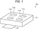
- Fig. 1 is an explanatory diagram illustrating an exemplary external appearance of the sensor module according to the embodiment of the present disclosure.
- Fig. 1 will be used to describe the exemplary external appearance of the sensor module according to the embodiment of the present disclosure.
- a sensor module 100 illustrated in Fig. 1 is a sensor module that may be installed in a portable device carried by a user, such as a smartphone, a tablet terminal, a game console, or a portable music player, for example.
- the sensor module 100 according to the embodiment of the present disclosure includes a housing 110 and a rigid flexible board 120.
- Four lenses 111a to 111d are provided on the light-incident face of the housing 110. Note that although the present embodiment illustrates an example in which four lenses of the sensor module 100 are provided, the present disclosure is not limited to such an example.
- the sensor module 100 is provided with a bandpass filter inside the housing 110. Also, an image sensor is formed on the rigid flexible board 120. Additionally, in the sensor module 100 according to the present embodiment, the bandpass filter is divided into four regions, and against light passing through each of the four lenses 111a to 111d, light of a predetermined wavelength band (frequency band) is passed via the bandpass filter, and that light is made to irradiate the image sensor. By having such a configuration, the sensor module 100 according to the present embodiment is capable of generating image data exposed by light of different wavelength bands (frequency bands) in a single imaging.
- Fig. 2 is an explanatory diagram illustrating an exploded perspective view of the internal structure of the sensor module according to the embodiment of the present disclosure.
- Fig. 2 will be used to describe the internal structure of the sensor module according to the embodiment of the present disclosure.
- the housing 110 is provided with four lenses 111a to 111d. Additionally, the interior of the housing 110 is divided into four regions 110a to 110d as illustrated in Fig. 2 .
- a bandpass filter 112 passes light of a predetermined frequency band wavelength band (frequency band) against light passing through the four lenses 111a to 111d. Additionally, in the present embodiment, the bandpass filter 112 includes four bandpass filters 112a to 112d having respectively different pass patterns. Light that has passed through the lens 111a passes through the bandpass filter 112a. Similarly, light that has passed through the lens 111b passes through the bandpass filter 112b, light that has passed through the lens 111c passes through the bandpass filter 112c, and light that has passed through the lens 111d passes through the bandpass filter 112d. Light that has passed through the bandpass filter 112 is radiated onto an image sensor 121.
- the image sensor 121 is an image sensor provided with a charge-coupled device (CCD) or complementary metal-oxide semiconductor (CMOS) imaging element, for example, and converts light that has passed through the bandpass filter 112 into an electric signal.
- CCD charge-coupled device
- CMOS complementary metal-oxide semiconductor
- the image sensor 121 is divided into four regions 121a to 121d, and respectively converts light that has passed through the bandpass filters 112a to 112d into electric signals.
- the image sensor 121 is provided with color filters on top of the imaging element.
- an effective region of the image sensor 121 refers to a region irradiated by light through a lens.
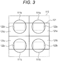
- Fig. 3 is an explanatory diagram illustrating effective regions of the image sensor 121, and is a diagram illustrating the state of the sensor module 100 as viewed from the side on which the lenses 111a to 111d are provided. As illustrated in Fig. 3 , by providing the lenses 111a to 111d, four effective regions 122a to 122d exist on the image sensor 121. The image sensor 121 generates image data by photoelectrically converting light radiated onto the effective regions 122a to 122d.
- pupil correction may also be performed such that incident light passing through the lenses 111a to 111d is made to irradiate the image sensor 121 efficiently.
- Pupil correction is a correction that adjusts the lenses 111a to 111d to match the angle of incidence of light rays in a central part and a peripheral part of the lenses 111a to 111d.
- the sensor module 100 according to the embodiment of the present disclosure is provided with the bandpass filter 112 that includes four bandpass filters 112a to 112d having different pass patterns.
- Each of the bandpass filters 112a to 112d is a bandpass filter that passes light of a predetermined range of wavelength bands while attenuating light of other wavelength bands, or alternatively is a combination of such bandpass filters.
- blue, green and red color filters corresponding to the three primary colors of light are provided in a Bayer array.
- the image sensor 121 of the present embodiment is characterized by being provided with a color filter having a different array for each region for extracting the component of a desired frequency band.
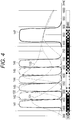
- Fig. 4 is an explanatory diagram illustrating a graph of exemplary characteristics of blue, green, and red color filters corresponding to the three primary colors of light and exemplary characteristics of bandpass filters used in the sensor module 100 according to the embodiment of the present disclosure.
- the sign 131 denotes the characteristics of the blue color filter
- the sign 132 denotes the characteristics of the green color filter
- the sign 133 denotes the characteristics of the red color filter.
- the signs 141 to 147 denote exemplary characteristics of bandpass filters used in the sensor module 100 according to the embodiment of the present disclosure.
- the bandpass filters used in the sensor module 100 are designated BPF1, BPF2, ..., BPF7 in order of shortest wavelength.
- the bandpass filters 112a to 112d have at least one from among BPF1 to BPF7.
- 500 nm to 550 nm is a wavelength band in which the chlorophyll of vegetables and plants is easily visualized. Consequently, in the case of wanting to use the sensor module 100 for the purpose of visualizing the chlorophyll of vegetables and plants, it is desirable to create and incorporate into the sensor module 100 a bandpass including BPF3.
- 550 nm to 600 nm is a wavelength band in which metmyoglobin, a causative agent that turns brown as meat gets older, is easily visualized, and therefore is a wavelength band in which the deterioration of meat is easily visualized. Consequently, in the case of wanting to use the sensor module 100 for the purpose of visualizing the deterioration of meat, it is desirable to create and incorporate into the sensor module 100 a bandpass including BPF4.
- 600 nm to 650 nm is a wavelength band in which lycopene contained in tomatoes or the like is easily visualized. Consequently, in the case of wanting to use the sensor module 100 for the purpose of visualizing lycopene, it is desirable to create and incorporate into the sensor module 100 a bandpass including BPF5.
- 650 nm to 700 nm is a wavelength band in which components associated with the freshness of meat are easily visualized. Consequently, in the case of wanting to use the sensor module 100 for the purpose of visualizing components associated with the freshness of meat, it is desirable to create and incorporate into the sensor module 100 a bandpass including BPF6.
- 800 nm to 900 nm is a wavelength band in which the water content contained in vegetables and plants is easily visualized. Consequently, in the case of wanting to use the sensor module 100 for the purpose of visualizing the water content contained in vegetables and plants, it is desirable to create and incorporate into the sensor module 100 a bandpass including BPF7.
- the sensor module 100 is capable of accommodating these uses with a single sensor module 100.
- the color filters provided in the image sensor 121 are treated as color filters in a Bayer array using the three primary colors of light, namely, blue, green, and red, color filters with low sensitivity to light that has passed through the bandpass filter 112 will exist.
- sensitivity is not obtained for wavelengths in the bands of 400 nm to 450 nm passed by BPF1 and 600 nm to 650 nm passed by BPF5. Consequently, for regions in which BPF1 or BPF5 is provided, little to no information is obtained from the green pixels. Therefore, the green pixels are wasted.
- the sensor module 100 to separate the components of the seven frequency bands described above from light that has passed through each of the bandpass filters 112a to 112d and also efficiently obtain information about the light that has passed through the bandpass filters 112a to 112d, color filters that correspond to the frequency band passed by each of the bandpass filters 112a to 112d are provided in the image sensor 121.
- color filters with an increased number of pixels from which information about light that has passed through the bandpass filters 112a to 112d is obtained are provided in the image sensor 121.
- the sensor module 100 according to the present embodiment is capable of accommodating a variety of uses by changing the combination of bandpass filters. For example, in cases in which it is difficult to discriminate between a human face and an elaborately crafted doll or the face of a mannequin by simply performing image processing alone, the change in the spectral reflectance of skin around certain wavelengths may be utilized, and bandpass filters that transmit light of those wavelengths may be provided in the sensor module 100. In this way, by providing bandpass filters that transmit the light of wavelengths at which the spectral reflectance of skin changes, the sensor module 100 according to the present embodiment may be used for biometric authentication.
- Fig. 5 is an explanatory diagram illustrating an example of bandpass filters configured as the bandpass filters 112a to 112d and color filters provided in the image sensor 121 in correspondence with each of the bandpass filters 112a to 112d.
- the bandpass filter 112a includes BPF1 and BPF4.
- the bandpass filter 112b includes BPF2 and BPF5.
- the bandpass filter 112c includes BPF3 and BPF6.
- the bandpass filter 112d includes BPF7.
- the color filters provided in the image sensor 121 are formed such that the components of the frequency bands passed by each of the bandpass filters 112a to 112d are obtained.
- the bandpass filter 112a includes BPF1 and BPF4, in the region of the bandpass filter 112a, pixels that pair with the blue color filter and pixels without a color filter (black-and-white pixels) are arranged in a check pattern.
- the bandpass filter 112b includes BPF2 and BPF5, in the region of the bandpass filter 112b, pixels that pair with the red color filter and pixels that pair with the blue color filter are arranged in a check pattern.
- the bandpass filter 112c includes BPF3 and BPF6, in the region of the bandpass filter 112c, pixels that pair with the green color filter and pixels that pair with the red color filter are arranged in a check pattern. Since the bandpass filter 112d includes BPF7, in the region of the bandpass filter 112c, pixels without a color filter (black-and-white pixels) are arranged.
- the sensor module 100 forms a pixel array capable of extracting the component of each frequency band efficiently. Furthermore, the sensor module 100 according to the present embodiment is capable of extracting, in a single imaging, the components of seven desired frequency bands with four types of bandpass filters and ordinary color filters using the three primary colors of light, namely blue, green, and red.
- Figs. 6 to 9 are explanatory diagrams illustrating exemplary characteristics of the bandpass filter 112a.
- the bandpass filter 112a includes BPF1 and BPF4
- light in the wavelength bands as illustrated in Fig. 6 is passed, whereas light in other wavelength bands is attenuated.
- the bandpass filter 112b includes BPF2 and BPF5, light in the wavelength bands as illustrated in Fig. 7 is passed, whereas light in other wavelength bands is attenuated.
- the bandpass filter 112c includes BPF3 and BPF6, light in the wavelength bands as illustrated in Fig. 8 is passed, whereas light in other wavelength bands is attenuated.
- the bandpass filter 112d includes BPF7, light in the wavelength band as illustrated in Fig. 9 is passed, whereas light in other wavelength bands is attenuated.
- the sensor module 100 By overlaying the four sorts of bandpass filters and color filters described above onto the single image sensor 121, the sensor module 100 according to the present embodiment is capable of generating image data appropriate to at least four sorts of uses.
- the bandpass filter 112a of the region 110a includes BPF1 and BPF5
- the bandpass filter 112b of the region 110b includes BPF2 and BPF6
- the bandpass filter 112c of the region 110c includes BPF3 and BPF7
- the bandpass filter 112d of the region 110d includes BPF4.
- pixels that pair with the blue color filter and pixels that pair with the red color filter are arranged in a check pattern.
- pixels that pair with the blue color filter and pixels that pair with the red color filter are arranged in a check pattern.
- pixels that pair with the green color filter and pixels without a color filter are arranged in a check pattern.
- pixels without a color filter are arranged in the region of the bandpass filter 112d.
- the sensor module 100 is capable of extracting, in a single imaging, the components of seven desired frequency bands with four types of bandpass filters and ordinary color filters using the three primary colors of light, namely blue, green, and red.
- the bandpass filter 112a of the region 110a includes BPF1 and BPF5
- the bandpass filter 112b of the region 110b includes BPF2 and BPF6
- the bandpass filter 112c of the region 110c includes BPF3 and BPF7
- the bandpass filter 112d of the region 110d includes BPF4.
- pixels that pair with the red color filter and pixels without a color filter are arranged in a check pattern.
- the component of the frequency band of BPF5 can be extracted by the pixels that pair with the red color filter.
- the component of the frequency band of BPF1 can be extracted by subtracting that which is obtained by the pixels that pair with the red color filter from that which is obtained by the pixels without a color filter (black-and-white pixels).
- pixels that pair with the blue color filter and pixels without a color filter are arranged in a check pattern.
- the component of the frequency band of BPF2 can be extracted by the pixels that pair with the blue color filter.
- the component of the frequency band of BPF6 can be extracted by subtracting that which is obtained by the pixels that pair with the blue color filter from that which is obtained by the pixels without a color filter (black-and-white pixels).
- pixels that pair with the green color filter and pixels without a color filter are arranged in a check pattern.
- the component of the frequency band of BPF3 can be extracted by the pixels that pair with the green color filter.
- the component of the frequency band of BPF7 can be extracted by the pixels without a color filter (black-and-white pixels).
- pixels without a color filter black-and-white pixels
- the component of the frequency band of BPF4 can be extracted by the pixels without a color filter (black-and-white pixels).
- the sensor module 100 becomes capable of extracting the components of desired frequency bands efficiently.
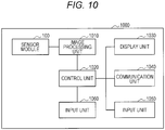
- Fig. 10 is an explanatory diagram illustrating an exemplary functional configuration of an information processing device 1000 incorporating the sensor module 100 according to the embodiment of the present disclosure.
- the information processing device 1000 includes the sensor module 100, an image processing unit 1010, a control unit 1020, a display unit 1030, a communication unit 1040, an input unit 1050, and a storage unit 1060.
- Image data generated by the sensor module 100 is sent to the image processing unit 1010.
- the image processing unit 1010 includes a circuit that executes image processing, such as a graphics processing unit (GPU), and executes various types of image processing on the image data output by the sensor module 100. For example, the image processing unit 1010 performs noise removal, partitioning into image data of each of the regions 121a to 121d of the image sensor 121, and the like.
- the image processing unit 1010 outputs the image-processed image data to the control unit 1020.
- the control unit 1020 includes a central processing unit (CPU), a micro-processing unit (MPU), or the like, and controls the operations of the information processing device 1000.
- CPU central processing unit
- MPU micro-processing unit
- the display unit 1030 includes a liquid crystal display or an organic EL display, for example.
- the display unit 1030 may also be provided with a touch panel that a user operates by touching a screen directly.
- the communication unit 1040 executes a process of communicating with another device by, for example, performing cellular communication, connecting to a wireless LAN or the like, or using a wireless communication standard such as infrared communication or Bluetooth (registered trademark).
- the input unit 1050 is a device for enabling the user to perform input operations, and may include for example a keyboard and mouse, a touch panel, or the like.
- the storage unit 1060 includes non-volatile or volatile memory, for example, holds programs and data necessary for operations of the information processing device 1000, and stores logs of operations of the information processing device 1000.
- Fig. 10 illustrates the information processing device 1000 incorporating only the sensor module 100 according to the embodiment of the present disclosure
- the present disclosure is not limited to such an example, and the information processing device 1000 may also incorporate a sensor module provided with color filters in an ordinary Bayer array in addition to the sensor module 100.
- the information processing device 1000 by being provided with the sensor module 100 according to the embodiment of the present disclosure, is capable of obtaining image data to be used for a variety of purposes with a single imaging process.
- the information processing device 1000 provided with the sensor module 100 according to the embodiment of the present disclosure can be used to visualize the state of chlorophyll and water content in vegetables and plants or to visualize components associated with the deterioration and freshness of meat as described above.
- the sensor module 100 capable of generating image data exposed by light of different wavelength bands (frequency bands) in a single imaging process, as well as the information processing device 1000 provided with such a sensor module 100.
Landscapes
- Physics & Mathematics (AREA)
- Engineering & Computer Science (AREA)
- Multimedia (AREA)
- Signal Processing (AREA)
- General Physics & Mathematics (AREA)
- Optics & Photonics (AREA)
- Color Television Image Signal Generators (AREA)
- Solid State Image Pick-Up Elements (AREA)
- Optical Filters (AREA)
Abstract
Description
- The present disclosure relates to a solid-state imaging device and an information processing device.
- For example,
Patent Literature 1 discloses technology related to a compound-eye camera module provided with a plurality of lenses. - Patent Document 1: Japanese Patent Application Laid-Open No.
2009-164654 - An object of the compound-eye camera module described in
Patent Literature 1 above is to measure the distance to a subject. By providing a plurality of lenses, it is possible to obtain a plurality of image data in a single imaging. - Accordingly, the present disclosure proposes a novel and improved solid-state imaging device and information processing device capable of generating image data exposed by light of different wavelengths in a single imaging.
- According to the present disclosure, there is provided a solid-state imaging device including: a plurality of lenses configured to condense light; a filter unit having a plurality of regions respectively irradiated by light passing through the plurality of lenses, the plurality of regions including transmission patterns configured to transmit different wavelength bands of the light; and an image sensor in which pixels configured to convert light transmitted through the filter unit into electric signals are arranged in a matrix, the image sensor being provided with color filters that correspond to the transmission patterns on a filter-unit side of the pixels.
- Also, according to the present disclosure, an information processing device provided with the above solid-state imaging device is provided.
- According to the present disclosure as described above, it is possible to provide a novel and improved solid-state imaging device and information processing device capable of generating image data exposed by light of different wavelengths in a single imaging.
- Note that the above effects are not strictly limiting, and that any effect indicated in the present disclosure or another effect that may be reasoned from the present disclosure may also be exhibited in addition to, or instead of, the above effects.
-
-
Fig. 1 is an explanatory diagram illustrating an exemplary external appearance of a sensor module according to an embodiment of the present disclosure. -
Fig. 2 is an explanatory diagram illustrating an exploded perspective view of the internal structure of the sensor module according to the embodiment. -
Fig. 3 is an explanatory diagram illustrating the effective region of an image sensor. -
Fig. 4 is an explanatory diagram illustrating a graph of exemplary characteristics of blue, green, and red color filters corresponding to the three primary colors of light and exemplary characteristics of bandpass filters used in the sensor module according to the embodiment. -
Fig. 5 is an explanatory diagram illustrating an example of a bandpass filter. -
Fig. 6 is an explanatory diagram illustrating exemplary characteristics of a bandpass filter. -
Fig. 7 is an explanatory diagram illustrating exemplary characteristics of a bandpass filter. -
Fig. 8 is an explanatory diagram illustrating exemplary characteristics of a bandpass filter. -
Fig. 9 is an explanatory diagram illustrating exemplary characteristics of a bandpass filter. -
Fig. 10 is an explanatory diagram illustrating an exemplary functional configuration of an information processing device incorporating the sensor module according to the embodiment. - Hereinafter, (a) preferred embodiment(s) of the present disclosure will be described in detail with reference to the appended drawings. Note that, in this specification and the appended drawings, structural elements that have substantially the same function and configuration are denoted with the same reference numerals, and repeated explanation of these structural elements is omitted.
- Note that, hereinafter, the description will proceed in the following order.
- 1. Embodiment of present disclosure
- 1.1. Exemplary external appearance of sensor module
- 1.2. Functions of sensor module
- 1.3. Exemplary configuration of device provided with sensor module
- 2. Conclusion
- First, an exemplary external appearance of the sensor module according to an embodiment of the present disclosure will be described with reference to the drawings.
Fig. 1 is an explanatory diagram illustrating an exemplary external appearance of the sensor module according to the embodiment of the present disclosure. Hereinafter,Fig. 1 will be used to describe the exemplary external appearance of the sensor module according to the embodiment of the present disclosure. - A
sensor module 100 illustrated inFig. 1 is a sensor module that may be installed in a portable device carried by a user, such as a smartphone, a tablet terminal, a game console, or a portable music player, for example. As illustrated inFig. 1 , thesensor module 100 according to the embodiment of the present disclosure includes ahousing 110 and a rigidflexible board 120. Fourlenses 111a to 111d are provided on the light-incident face of thehousing 110. Note that although the present embodiment illustrates an example in which four lenses of thesensor module 100 are provided, the present disclosure is not limited to such an example. - As described later, the
sensor module 100 is provided with a bandpass filter inside thehousing 110. Also, an image sensor is formed on the rigidflexible board 120. Additionally, in thesensor module 100 according to the present embodiment, the bandpass filter is divided into four regions, and against light passing through each of the fourlenses 111a to 111d, light of a predetermined wavelength band (frequency band) is passed via the bandpass filter, and that light is made to irradiate the image sensor. By having such a configuration, thesensor module 100 according to the present embodiment is capable of generating image data exposed by light of different wavelength bands (frequency bands) in a single imaging. - The above describes an exemplary external appearance of the sensor module according to the embodiment of the present disclosure. Next, the internal structure of the sensor module according to the embodiment of the present disclosure will be described using an exploded perspective view.
-
Fig. 2 is an explanatory diagram illustrating an exploded perspective view of the internal structure of the sensor module according to the embodiment of the present disclosure. Hereinafter,Fig. 2 will be used to describe the internal structure of the sensor module according to the embodiment of the present disclosure. - As described above, the
housing 110 is provided with fourlenses 111a to 111d. Additionally, the interior of thehousing 110 is divided into fourregions 110a to 110d as illustrated inFig. 2 . - A
bandpass filter 112 passes light of a predetermined frequency band wavelength band (frequency band) against light passing through the fourlenses 111a to 111d. Additionally, in the present embodiment, thebandpass filter 112 includes fourbandpass filters 112a to 112d having respectively different pass patterns. Light that has passed through thelens 111a passes through thebandpass filter 112a. Similarly, light that has passed through thelens 111b passes through thebandpass filter 112b, light that has passed through thelens 111c passes through thebandpass filter 112c, and light that has passed through thelens 111d passes through thebandpass filter 112d. Light that has passed through thebandpass filter 112 is radiated onto animage sensor 121. - The
image sensor 121 is an image sensor provided with a charge-coupled device (CCD) or complementary metal-oxide semiconductor (CMOS) imaging element, for example, and converts light that has passed through thebandpass filter 112 into an electric signal. In the present embodiment, theimage sensor 121 is divided into fourregions 121a to 121d, and respectively converts light that has passed through thebandpass filters 112a to 112d into electric signals. Also, theimage sensor 121 is provided with color filters on top of the imaging element. - The above describes the internal structure of the sensor module according to the embodiment of the present disclosure using an exploded perspective view. Next, effective regions of the
image sensor 121 provided in the sensor module according to the embodiment of the present disclosure will be described. Herein, an effective region of theimage sensor 121 refers to a region irradiated by light through a lens. -
Fig. 3 is an explanatory diagram illustrating effective regions of theimage sensor 121, and is a diagram illustrating the state of thesensor module 100 as viewed from the side on which thelenses 111a to 111d are provided. As illustrated inFig. 3 , by providing thelenses 111a to 111d, foureffective regions 122a to 122d exist on theimage sensor 121. Theimage sensor 121 generates image data by photoelectrically converting light radiated onto theeffective regions 122a to 122d. - Note that in the case in which the
lenses 111a to 111d are provided above theimage sensor 121 in this way, pupil correction may also be performed such that incident light passing through thelenses 111a to 111d is made to irradiate theimage sensor 121 efficiently. Pupil correction is a correction that adjusts thelenses 111a to 111d to match the angle of incidence of light rays in a central part and a peripheral part of thelenses 111a to 111d. - Next, functions of the sensor module according to the embodiment of the present disclosure will be described. As described above, the
sensor module 100 according to the embodiment of the present disclosure is provided with thebandpass filter 112 that includes fourbandpass filters 112a to 112d having different pass patterns. Each of thebandpass filters 112a to 112d is a bandpass filter that passes light of a predetermined range of wavelength bands while attenuating light of other wavelength bands, or alternatively is a combination of such bandpass filters. - In an ordinary sensor module, blue, green and red color filters corresponding to the three primary colors of light are provided in a Bayer array. Rather than being provided with color filters based on the above three primary colors of light, namely blue, green, and red, as described later, the
image sensor 121 of the present embodiment is characterized by being provided with a color filter having a different array for each region for extracting the component of a desired frequency band. -
Fig. 4 is an explanatory diagram illustrating a graph of exemplary characteristics of blue, green, and red color filters corresponding to the three primary colors of light and exemplary characteristics of bandpass filters used in thesensor module 100 according to the embodiment of the present disclosure. Thesign 131 denotes the characteristics of the blue color filter, thesign 132 denotes the characteristics of the green color filter, and thesign 133 denotes the characteristics of the red color filter. In contrast, thesigns 141 to 147 denote exemplary characteristics of bandpass filters used in thesensor module 100 according to the embodiment of the present disclosure. In the following description, the bandpass filters used in thesensor module 100 are designated BPF1, BPF2, ..., BPF7 in order of shortest wavelength. Additionally, thebandpass filters 112a to 112d have at least one from among BPF1 to BPF7. - For example, 500 nm to 550 nm is a wavelength band in which the chlorophyll of vegetables and plants is easily visualized. Consequently, in the case of wanting to use the
sensor module 100 for the purpose of visualizing the chlorophyll of vegetables and plants, it is desirable to create and incorporate into the sensor module 100 a bandpass including BPF3. - In addition, as another example, 550 nm to 600 nm is a wavelength band in which metmyoglobin, a causative agent that turns brown as meat gets older, is easily visualized, and therefore is a wavelength band in which the deterioration of meat is easily visualized. Consequently, in the case of wanting to use the
sensor module 100 for the purpose of visualizing the deterioration of meat, it is desirable to create and incorporate into the sensor module 100 a bandpass including BPF4. - In addition, for example, 600 nm to 650 nm is a wavelength band in which lycopene contained in tomatoes or the like is easily visualized. Consequently, in the case of wanting to use the
sensor module 100 for the purpose of visualizing lycopene, it is desirable to create and incorporate into the sensor module 100 a bandpass including BPF5. - In addition, for example, 650 nm to 700 nm is a wavelength band in which components associated with the freshness of meat are easily visualized. Consequently, in the case of wanting to use the
sensor module 100 for the purpose of visualizing components associated with the freshness of meat, it is desirable to create and incorporate into the sensor module 100 a bandpass including BPF6. - In addition, for example, 800 nm to 900 nm is a wavelength band in which the water content contained in vegetables and plants is easily visualized. Consequently, in the case of wanting to use the
sensor module 100 for the purpose of visualizing the water content contained in vegetables and plants, it is desirable to create and incorporate into the sensor module 100 a bandpass including BPF7. - Additionally, by configuring the
bandpass filter 112 with the plurality ofbandpass filters 112a to 112d, thesensor module 100 according to the present embodiment is capable of accommodating these uses with asingle sensor module 100. - However, if the color filters provided in the
image sensor 121 are treated as color filters in a Bayer array using the three primary colors of light, namely, blue, green, and red, color filters with low sensitivity to light that has passed through thebandpass filter 112 will exist. For example, in pixels assigned to a green color filter, sensitivity is not obtained for wavelengths in the bands of 400 nm to 450 nm passed by BPF1 and 600 nm to 650 nm passed by BPF5. Consequently, for regions in which BPF1 or BPF5 is provided, little to no information is obtained from the green pixels. Therefore, the green pixels are wasted. - Accordingly, the
sensor module 100 according to the present embodiment, to separate the components of the seven frequency bands described above from light that has passed through each of thebandpass filters 112a to 112d and also efficiently obtain information about the light that has passed through thebandpass filters 112a to 112d, color filters that correspond to the frequency band passed by each of thebandpass filters 112a to 112d are provided in theimage sensor 121. In other words, compared to color filters in a Bayer array, color filters with an increased number of pixels from which information about light that has passed through thebandpass filters 112a to 112d is obtained are provided in theimage sensor 121. - Besides the uses described above, the
sensor module 100 according to the present embodiment is capable of accommodating a variety of uses by changing the combination of bandpass filters. For example, in cases in which it is difficult to discriminate between a human face and an elaborately crafted doll or the face of a mannequin by simply performing image processing alone, the change in the spectral reflectance of skin around certain wavelengths may be utilized, and bandpass filters that transmit light of those wavelengths may be provided in thesensor module 100. In this way, by providing bandpass filters that transmit the light of wavelengths at which the spectral reflectance of skin changes, thesensor module 100 according to the present embodiment may be used for biometric authentication. -
Fig. 5 is an explanatory diagram illustrating an example of bandpass filters configured as thebandpass filters 112a to 112d and color filters provided in theimage sensor 121 in correspondence with each of thebandpass filters 112a to 112d. In the example illustrated inFig. 5 , thebandpass filter 112a includes BPF1 and BPF4. Similarly, thebandpass filter 112b includes BPF2 and BPF5. Also similarly, thebandpass filter 112c includes BPF3 and BPF6. Also similarly, thebandpass filter 112d includes BPF7. - In addition, the color filters provided in the
image sensor 121 are formed such that the components of the frequency bands passed by each of thebandpass filters 112a to 112d are obtained. Since thebandpass filter 112a includes BPF1 and BPF4, in the region of thebandpass filter 112a, pixels that pair with the blue color filter and pixels without a color filter (black-and-white pixels) are arranged in a check pattern. Since thebandpass filter 112b includes BPF2 and BPF5, in the region of thebandpass filter 112b, pixels that pair with the red color filter and pixels that pair with the blue color filter are arranged in a check pattern. Since thebandpass filter 112c includes BPF3 and BPF6, in the region of thebandpass filter 112c, pixels that pair with the green color filter and pixels that pair with the red color filter are arranged in a check pattern. Since thebandpass filter 112d includes BPF7, in the region of thebandpass filter 112c, pixels without a color filter (black-and-white pixels) are arranged. - In this way, by forming color filters such that the components of the frequency bands passed by each of the
bandpass filters 112a to 112d are obtained, thesensor module 100 according to the present embodiment forms a pixel array capable of extracting the component of each frequency band efficiently. Furthermore, thesensor module 100 according to the present embodiment is capable of extracting, in a single imaging, the components of seven desired frequency bands with four types of bandpass filters and ordinary color filters using the three primary colors of light, namely blue, green, and red. -
Figs. 6 to 9 are explanatory diagrams illustrating exemplary characteristics of thebandpass filter 112a. Since thebandpass filter 112a includes BPF1 and BPF4, light in the wavelength bands as illustrated inFig. 6 is passed, whereas light in other wavelength bands is attenuated. Since thebandpass filter 112b includes BPF2 and BPF5, light in the wavelength bands as illustrated inFig. 7 is passed, whereas light in other wavelength bands is attenuated. Since thebandpass filter 112c includes BPF3 and BPF6, light in the wavelength bands as illustrated inFig. 8 is passed, whereas light in other wavelength bands is attenuated. Additionally, since thebandpass filter 112d includes BPF7, light in the wavelength band as illustrated inFig. 9 is passed, whereas light in other wavelength bands is attenuated. - By overlaying the four sorts of bandpass filters and color filters described above onto the
single image sensor 121, thesensor module 100 according to the present embodiment is capable of generating image data appropriate to at least four sorts of uses. - A different example will be illustrated. In this example, assume that the
bandpass filter 112a of theregion 110a includes BPF1 and BPF5, thebandpass filter 112b of theregion 110b includes BPF2 and BPF6, thebandpass filter 112c of theregion 110c includes BPF3 and BPF7, and thebandpass filter 112d of theregion 110d includes BPF4. - In this case, in the region of the
bandpass filter 112a, pixels that pair with the blue color filter and pixels that pair with the red color filter are arranged in a check pattern. In the region of thebandpass filter 112b, pixels that pair with the blue color filter and pixels that pair with the red color filter are arranged in a check pattern. In the region of thebandpass filter 112c, pixels that pair with the green color filter and pixels without a color filter (black-and-white pixels) are arranged in a check pattern. In the region of thebandpass filter 112d, pixels without a color filter (black-and-white pixels) are arranged. Thus, by forming the color filter on theimage sensor 121, thesensor module 100 is capable of extracting, in a single imaging, the components of seven desired frequency bands with four types of bandpass filters and ordinary color filters using the three primary colors of light, namely blue, green, and red. - A different example will be illustrated. Also in this example, assume that the
bandpass filter 112a of theregion 110a includes BPF1 and BPF5, thebandpass filter 112b of theregion 110b includes BPF2 and BPF6, thebandpass filter 112c of theregion 110c includes BPF3 and BPF7, and thebandpass filter 112d of theregion 110d includes BPF4. - In this case, in the region of the
bandpass filter 112a, pixels that pair with the red color filter and pixels without a color filter (black-and-white pixels) are arranged in a check pattern. The component of the frequency band of BPF5 can be extracted by the pixels that pair with the red color filter. On the other hand, the component of the frequency band of BPF1 can be extracted by subtracting that which is obtained by the pixels that pair with the red color filter from that which is obtained by the pixels without a color filter (black-and-white pixels). - Furthermore, in the region of the
bandpass filter 112b, pixels that pair with the blue color filter and pixels without a color filter (black-and-white pixels) are arranged in a check pattern. The component of the frequency band of BPF2 can be extracted by the pixels that pair with the blue color filter. On the other hand, the component of the frequency band of BPF6 can be extracted by subtracting that which is obtained by the pixels that pair with the blue color filter from that which is obtained by the pixels without a color filter (black-and-white pixels). - Furthermore, in the region of the
bandpass filter 112c, pixels that pair with the green color filter and pixels without a color filter (black-and-white pixels) are arranged in a check pattern. The component of the frequency band of BPF3 can be extracted by the pixels that pair with the green color filter. On the other hand, the component of the frequency band of BPF7 can be extracted by the pixels without a color filter (black-and-white pixels). Also, in the region of thebandpass filter 112d, pixels without a color filter (black-and-white pixels) are arranged. The component of the frequency band of BPF4 can be extracted by the pixels without a color filter (black-and-white pixels). - In this way, by appropriately combining color filters, the
sensor module 100 according to the embodiment of the present disclosure becomes capable of extracting the components of desired frequency bands efficiently. - Next, an exemplary functional configuration of an information processing device incorporating the
sensor module 100 according to the embodiment of the present disclosure will be described. -
Fig. 10 is an explanatory diagram illustrating an exemplary functional configuration of aninformation processing device 1000 incorporating thesensor module 100 according to the embodiment of the present disclosure. As illustrated inFig. 10 , theinformation processing device 1000 includes thesensor module 100, animage processing unit 1010, acontrol unit 1020, adisplay unit 1030, acommunication unit 1040, aninput unit 1050, and astorage unit 1060. - Image data generated by the
sensor module 100 is sent to theimage processing unit 1010. Theimage processing unit 1010 includes a circuit that executes image processing, such as a graphics processing unit (GPU), and executes various types of image processing on the image data output by thesensor module 100. For example, theimage processing unit 1010 performs noise removal, partitioning into image data of each of theregions 121a to 121d of theimage sensor 121, and the like. Theimage processing unit 1010 outputs the image-processed image data to thecontrol unit 1020. - The
control unit 1020 includes a central processing unit (CPU), a micro-processing unit (MPU), or the like, and controls the operations of theinformation processing device 1000. - The
display unit 1030 includes a liquid crystal display or an organic EL display, for example. Thedisplay unit 1030 may also be provided with a touch panel that a user operates by touching a screen directly. Thecommunication unit 1040 executes a process of communicating with another device by, for example, performing cellular communication, connecting to a wireless LAN or the like, or using a wireless communication standard such as infrared communication or Bluetooth (registered trademark). Theinput unit 1050 is a device for enabling the user to perform input operations, and may include for example a keyboard and mouse, a touch panel, or the like. Thestorage unit 1060 includes non-volatile or volatile memory, for example, holds programs and data necessary for operations of theinformation processing device 1000, and stores logs of operations of theinformation processing device 1000. - Note that although
Fig. 10 illustrates theinformation processing device 1000 incorporating only thesensor module 100 according to the embodiment of the present disclosure, the present disclosure is not limited to such an example, and theinformation processing device 1000 may also incorporate a sensor module provided with color filters in an ordinary Bayer array in addition to thesensor module 100. - The
information processing device 1000, by being provided with thesensor module 100 according to the embodiment of the present disclosure, is capable of obtaining image data to be used for a variety of purposes with a single imaging process. For example, theinformation processing device 1000 provided with thesensor module 100 according to the embodiment of the present disclosure can be used to visualize the state of chlorophyll and water content in vegetables and plants or to visualize components associated with the deterioration and freshness of meat as described above. - According to the embodiment of the present disclosure as described above, there is provided the
sensor module 100 capable of generating image data exposed by light of different wavelength bands (frequency bands) in a single imaging process, as well as theinformation processing device 1000 provided with such asensor module 100. - The preferred embodiment(s) of the present disclosure has/have been described above with reference to the accompanying drawings, whilst the present disclosure is not limited to the above examples. A person skilled in the art may find various alterations and modifications within the scope of the appended claims, and it should be understood that they will naturally come under the technical scope of the present disclosure.
- Further, the effects described in this specification are merely illustrative or exemplified effects, and are not limitative. That is, with or in the place of the above effects, the technology according to the present disclosure may achieve other effects that are clear to those skilled in the art from the description of this specification.
- Additionally, the present disclosure may also be configured as below.
- (1) A solid-state imaging device including:
- a plurality of lenses configured to condense light;
- a filter unit having a plurality of regions respectively irradiated by light passing through the plurality of lenses, the plurality of regions including transmission patterns configured to transmit different wavelength bands of the light; and
- an image sensor in which pixels configured to convert light transmitted through the filter unit into electric signals are arranged in a matrix, the image sensor being provided with color filters that correspond to the transmission patterns on a filter-unit side of the pixels.
- (2) The solid-state imaging device according to (1), in which the transmission patterns are at least one selected from among bandpass filters configured to transmit respectively different wavelength bands.
- (3) The solid-state imaging device according to (2), in which the transmission patterns are two bandpass filters having non-adjacent wavelength bands selected from among the bandpass filters configured to transmit respectively different wavelength bands.
- (4) The solid-state imaging device according to (2) or (3), in which the wavelength bands transmitted by the bandpass filters are set in intervals of at least 50 nm.
- (5) The solid-state imaging device according to any one of () to (4), in which the color filters are formed in correspondence with each of the pixels of the image sensor.
- (6) An information processing device including: the solid-state imaging device according to any one of (1) to (5) .
-
- 100
- Sensor module
- 110
- Housing
- 111a
- Lens
- 111b
- Lens
- 111c
- Lens
- 111d
- Lens
- 112
- Bandpass filter
- 112a
- Bandpass filter
- 112b
- Bandpass filter
- 112c
- Bandpass filter
- 112d
- Bandpass filter
- 120
- Rigid flexible board
- 121
- Image sensor
- 121a
- Region
- 121b
- Region
- 121c
- Region
- 121d
- Region
- 122a
- Effective region
- 122b
- Effective region
- 122c
- Effective region
- 122d
- Effective region
- 1000
- Information processing device
Claims (6)
- A solid-state imaging device comprising:a plurality of lenses configured to condense light;a filter unit having a plurality of regions respectively irradiated by light passing through the plurality of lenses, the plurality of regions including transmission patterns configured to transmit different wavelength bands of the light; andan image sensor in which pixels configured to convert light transmitted through the filter unit into electric signals are arranged in a matrix, the image sensor being provided with color filters that correspond to the transmission patterns on a filter-unit side of the pixels.
- The solid-state imaging device according to claim 1, wherein the transmission patterns are at least one selected from among bandpass filters configured to transmit respectively different wavelength bands.
- The solid-state imaging device according to claim 2, wherein the transmission patterns are two bandpass filters having non-adjacent wavelength bands selected from among the bandpass filters configured to transmit respectively different wavelength bands.
- The solid-state imaging device according to claim 2, wherein the wavelength bands transmitted by the bandpass filters are set in intervals of at least 50 nm.
- The solid-state imaging device according to claim 1, wherein the color filters are formed in correspondence with each of the pixels of the image sensor.
- An information processing device comprising: the solid-state imaging device according to claim 1.
Applications Claiming Priority (2)
| Application Number | Priority Date | Filing Date | Title |
|---|---|---|---|
| JP2017084523A JP6878111B2 (en) | 2017-04-21 | 2017-04-21 | Solid-state image sensor and information processing device |
| PCT/JP2018/007864 WO2018193727A1 (en) | 2017-04-21 | 2018-03-01 | Solid-state imaging apparatus and information processing apparatus |
Publications (3)
| Publication Number | Publication Date |
|---|---|
| EP3614435A1 true EP3614435A1 (en) | 2020-02-26 |
| EP3614435A4 EP3614435A4 (en) | 2020-04-22 |
| EP3614435B1 EP3614435B1 (en) | 2022-01-05 |
Family
ID=63857130
Family Applications (1)
| Application Number | Title | Priority Date | Filing Date |
|---|---|---|---|
| EP18787756.8A Active EP3614435B1 (en) | 2017-04-21 | 2018-03-01 | Solid-state imaging apparatus and information processing apparatus |
Country Status (4)
| Country | Link |
|---|---|
| US (1) | US11265520B2 (en) |
| EP (1) | EP3614435B1 (en) |
| JP (1) | JP6878111B2 (en) |
| WO (1) | WO2018193727A1 (en) |
Family Cites Families (20)
| Publication number | Priority date | Publication date | Assignee | Title |
|---|---|---|---|---|
| JPH11201819A (en) * | 1998-01-08 | 1999-07-30 | Minolta Co Ltd | Two-dimensional spectral characteristics measuring device |
| US6611289B1 (en) * | 1999-01-15 | 2003-08-26 | Yanbin Yu | Digital cameras using multiple sensors with multiple lenses |
| JP2003143459A (en) * | 2001-11-02 | 2003-05-16 | Canon Inc | Compound eye imaging system and apparatus equipped with the same |
| US7920908B2 (en) * | 2003-10-16 | 2011-04-05 | David Hattery | Multispectral imaging for quantitative contrast of functional and structural features of layers inside optically dense media such as tissue |
| JP2006122338A (en) * | 2004-10-28 | 2006-05-18 | Aruze Corp | Game machine and program |
| EP1952106B1 (en) * | 2005-11-04 | 2014-08-27 | George Themelis | System for multispectral imaging |
| JP2009164654A (en) * | 2006-04-24 | 2009-07-23 | Panasonic Corp | Compound eye camera module |
| WO2008074019A2 (en) * | 2006-12-13 | 2008-06-19 | Georgia Tech Research Corporation | Systems and methods for real time multispectral imaging |
| JP5332996B2 (en) * | 2009-07-17 | 2013-11-06 | ソニー株式会社 | Multilayer optical filter, solid-state imaging device, imaging device, display device, communication device |
| US20130331669A1 (en) * | 2012-06-11 | 2013-12-12 | Raytheon Company | Multi-spectral imaging system and method for remote biometric measurement of human physiological parameters |
| US9258495B2 (en) * | 2012-06-21 | 2016-02-09 | Providence Photonics, Llc | Multi-spectral infrared imaging system for flare combustion efficiency monitoring |
| CN105264419B (en) * | 2013-06-06 | 2017-09-22 | 富士胶片株式会社 | Autofocus and its method of controlling operation |
| JP6404923B2 (en) * | 2014-06-24 | 2018-10-17 | マクセル株式会社 | Imaging sensor and imaging apparatus |
| US9699393B2 (en) * | 2014-06-26 | 2017-07-04 | Semiconductor Components Industries, Llc | Imaging systems for infrared and visible imaging with patterned infrared cutoff filters |
| JP6536877B2 (en) * | 2014-07-31 | 2019-07-03 | パナソニックIpマネジメント株式会社 | Imaging device and imaging system |
| US9666620B2 (en) * | 2014-10-06 | 2017-05-30 | Visera Technologies Company Limited | Stacked filter and image sensor containing the same |
| US9972651B2 (en) * | 2015-08-03 | 2018-05-15 | Visera Technologies Company Limited | Spectrum-inspection device |
| KR102255789B1 (en) * | 2016-08-30 | 2021-05-26 | 삼성전자주식회사 | Optical Module and Optical device Using the same |
| CN110383047B (en) * | 2016-11-20 | 2022-06-07 | 尤尼斯拜特罗有限责任公司 | Multiband imaging system |
| EP3388885B1 (en) * | 2017-04-11 | 2025-07-30 | Leica Instruments (Singapore) Pte. Ltd. | Multiple band pass liquid crystal tunable filter |
-
2017
- 2017-04-21 JP JP2017084523A patent/JP6878111B2/en not_active Expired - Fee Related
-
2018
- 2018-03-01 US US16/497,447 patent/US11265520B2/en active Active
- 2018-03-01 EP EP18787756.8A patent/EP3614435B1/en active Active
- 2018-03-01 WO PCT/JP2018/007864 patent/WO2018193727A1/en not_active Ceased
Also Published As
| Publication number | Publication date |
|---|---|
| EP3614435B1 (en) | 2022-01-05 |
| US11265520B2 (en) | 2022-03-01 |
| WO2018193727A1 (en) | 2018-10-25 |
| JP2018182255A (en) | 2018-11-15 |
| US20200106994A1 (en) | 2020-04-02 |
| JP6878111B2 (en) | 2021-05-26 |
| EP3614435A4 (en) | 2020-04-22 |
Similar Documents
| Publication | Publication Date | Title |
|---|---|---|
| US11134848B2 (en) | Mobile hyperspectral camera system and human skin monitoring using a mobile hyperspectral camera system | |
| CN103826530B (en) | Camera system | |
| Gono | Narrow band imaging: technology basis and research and development history | |
| JP6524617B2 (en) | Imager and method | |
| US20200204776A1 (en) | Image-processing device, fluorescence observation device and method for emulating a first type of fluorescence observation device on a second type of fluorescence observation device | |
| AU2025248641A1 (en) | Hybrid visible and near infrared imaging with an rgb color filter array sensor | |
| US11202126B2 (en) | Simultaneous display of two or more different sequentially processed images | |
| JP2018107817A5 (en) | ||
| CN108769502A (en) | Camera treatment device and image pickup processing method | |
| US20210073505A1 (en) | Optical fingerprint identification assembly and terminal | |
| JP2004228662A (en) | Imaging device | |
| EP4307701A3 (en) | Sensing images using multiple band pass bayer pattern filter for discriminating lipid and collagen tissues | |
| KR20210062974A (en) | Electronic device and method for measuring vital signals | |
| CN113242964A (en) | Photoelectric sensor for color measurement | |
| US12165402B2 (en) | Image recognition device and image recognition method | |
| WO2022163671A1 (en) | Data processing device, method, and program, optical element, imaging optical system, and imaging device | |
| EP3614435B1 (en) | Solid-state imaging apparatus and information processing apparatus | |
| US12372404B2 (en) | Illuminant correction in an imaging system | |
| WO2016174778A1 (en) | Imaging device, image processing device, and image processing method | |
| CN114268774A (en) | Image acquisition method, image sensor, device, equipment and storage medium | |
| JP7830439B2 (en) | Solid-state imaging devices and electronic equipment | |
| CN111918004B (en) | Image sensor, terminal, data processing method, device and storage medium | |
| US20110080506A1 (en) | Image sensing device and system | |
| JP6759142B2 (en) | Biometric device and method | |
| US20240268678A1 (en) | Multi-modal skin imaging |
Legal Events
| Date | Code | Title | Description |
|---|---|---|---|
| STAA | Information on the status of an ep patent application or granted ep patent |
Free format text: STATUS: THE INTERNATIONAL PUBLICATION HAS BEEN MADE |
|
| PUAI | Public reference made under article 153(3) epc to a published international application that has entered the european phase |
Free format text: ORIGINAL CODE: 0009012 |
|
| STAA | Information on the status of an ep patent application or granted ep patent |
Free format text: STATUS: REQUEST FOR EXAMINATION WAS MADE |
|
| 17P | Request for examination filed |
Effective date: 20191011 |
|
| AK | Designated contracting states |
Kind code of ref document: A1 Designated state(s): AL AT BE BG CH CY CZ DE DK EE ES FI FR GB GR HR HU IE IS IT LI LT LU LV MC MK MT NL NO PL PT RO RS SE SI SK SM TR |
|
| AX | Request for extension of the european patent |
Extension state: BA ME |
|
| A4 | Supplementary search report drawn up and despatched |
Effective date: 20200323 |
|
| RIC1 | Information provided on ipc code assigned before grant |
Ipc: G02B 5/28 20060101ALI20200317BHEP Ipc: H01L 27/146 20060101AFI20200317BHEP Ipc: H04N 9/07 20060101ALI20200317BHEP Ipc: G02B 5/20 20060101ALI20200317BHEP |
|
| DAV | Request for validation of the european patent (deleted) | ||
| DAX | Request for extension of the european patent (deleted) | ||
| GRAP | Despatch of communication of intention to grant a patent |
Free format text: ORIGINAL CODE: EPIDOSNIGR1 |
|
| STAA | Information on the status of an ep patent application or granted ep patent |
Free format text: STATUS: GRANT OF PATENT IS INTENDED |
|
| INTG | Intention to grant announced |
Effective date: 20210810 |
|
| RAP1 | Party data changed (applicant data changed or rights of an application transferred) |
Owner name: SONY GROUP CORPORATION |
|
| GRAS | Grant fee paid |
Free format text: ORIGINAL CODE: EPIDOSNIGR3 |
|
| GRAA | (expected) grant |
Free format text: ORIGINAL CODE: 0009210 |
|
| STAA | Information on the status of an ep patent application or granted ep patent |
Free format text: STATUS: THE PATENT HAS BEEN GRANTED |
|
| AK | Designated contracting states |
Kind code of ref document: B1 Designated state(s): AL AT BE BG CH CY CZ DE DK EE ES FI FR GB GR HR HU IE IS IT LI LT LU LV MC MK MT NL NO PL PT RO RS SE SI SK SM TR |
|
| REG | Reference to a national code |
Ref country code: GB Ref legal event code: FG4D |
|
| REG | Reference to a national code |
Ref country code: CH Ref legal event code: EP |
|
| REG | Reference to a national code |
Ref country code: AT Ref legal event code: REF Ref document number: 1461346 Country of ref document: AT Kind code of ref document: T Effective date: 20220115 |
|
| REG | Reference to a national code |
Ref country code: DE Ref legal event code: R096 Ref document number: 602018029198 Country of ref document: DE |
|
| REG | Reference to a national code |
Ref country code: IE Ref legal event code: FG4D |
|
| REG | Reference to a national code |
Ref country code: LT Ref legal event code: MG9D |
|
| REG | Reference to a national code |
Ref country code: NL Ref legal event code: MP Effective date: 20220105 |
|
| REG | Reference to a national code |
Ref country code: AT Ref legal event code: MK05 Ref document number: 1461346 Country of ref document: AT Kind code of ref document: T Effective date: 20220105 |
|
| PG25 | Lapsed in a contracting state [announced via postgrant information from national office to epo] |
Ref country code: NL Free format text: LAPSE BECAUSE OF FAILURE TO SUBMIT A TRANSLATION OF THE DESCRIPTION OR TO PAY THE FEE WITHIN THE PRESCRIBED TIME-LIMIT Effective date: 20220105 |
|
| PG25 | Lapsed in a contracting state [announced via postgrant information from national office to epo] |
Ref country code: SE Free format text: LAPSE BECAUSE OF FAILURE TO SUBMIT A TRANSLATION OF THE DESCRIPTION OR TO PAY THE FEE WITHIN THE PRESCRIBED TIME-LIMIT Effective date: 20220105 Ref country code: RS Free format text: LAPSE BECAUSE OF FAILURE TO SUBMIT A TRANSLATION OF THE DESCRIPTION OR TO PAY THE FEE WITHIN THE PRESCRIBED TIME-LIMIT Effective date: 20220105 Ref country code: PT Free format text: LAPSE BECAUSE OF FAILURE TO SUBMIT A TRANSLATION OF THE DESCRIPTION OR TO PAY THE FEE WITHIN THE PRESCRIBED TIME-LIMIT Effective date: 20220505 Ref country code: NO Free format text: LAPSE BECAUSE OF FAILURE TO SUBMIT A TRANSLATION OF THE DESCRIPTION OR TO PAY THE FEE WITHIN THE PRESCRIBED TIME-LIMIT Effective date: 20220405 Ref country code: LT Free format text: LAPSE BECAUSE OF FAILURE TO SUBMIT A TRANSLATION OF THE DESCRIPTION OR TO PAY THE FEE WITHIN THE PRESCRIBED TIME-LIMIT Effective date: 20220105 Ref country code: HR Free format text: LAPSE BECAUSE OF FAILURE TO SUBMIT A TRANSLATION OF THE DESCRIPTION OR TO PAY THE FEE WITHIN THE PRESCRIBED TIME-LIMIT Effective date: 20220105 Ref country code: ES Free format text: LAPSE BECAUSE OF FAILURE TO SUBMIT A TRANSLATION OF THE DESCRIPTION OR TO PAY THE FEE WITHIN THE PRESCRIBED TIME-LIMIT Effective date: 20220105 Ref country code: BG Free format text: LAPSE BECAUSE OF FAILURE TO SUBMIT A TRANSLATION OF THE DESCRIPTION OR TO PAY THE FEE WITHIN THE PRESCRIBED TIME-LIMIT Effective date: 20220405 |
|
| PG25 | Lapsed in a contracting state [announced via postgrant information from national office to epo] |
Ref country code: PL Free format text: LAPSE BECAUSE OF FAILURE TO SUBMIT A TRANSLATION OF THE DESCRIPTION OR TO PAY THE FEE WITHIN THE PRESCRIBED TIME-LIMIT Effective date: 20220105 Ref country code: LV Free format text: LAPSE BECAUSE OF FAILURE TO SUBMIT A TRANSLATION OF THE DESCRIPTION OR TO PAY THE FEE WITHIN THE PRESCRIBED TIME-LIMIT Effective date: 20220105 Ref country code: GR Free format text: LAPSE BECAUSE OF FAILURE TO SUBMIT A TRANSLATION OF THE DESCRIPTION OR TO PAY THE FEE WITHIN THE PRESCRIBED TIME-LIMIT Effective date: 20220406 Ref country code: FI Free format text: LAPSE BECAUSE OF FAILURE TO SUBMIT A TRANSLATION OF THE DESCRIPTION OR TO PAY THE FEE WITHIN THE PRESCRIBED TIME-LIMIT Effective date: 20220105 Ref country code: AT Free format text: LAPSE BECAUSE OF FAILURE TO SUBMIT A TRANSLATION OF THE DESCRIPTION OR TO PAY THE FEE WITHIN THE PRESCRIBED TIME-LIMIT Effective date: 20220105 |
|
| PG25 | Lapsed in a contracting state [announced via postgrant information from national office to epo] |
Ref country code: IS Free format text: LAPSE BECAUSE OF FAILURE TO SUBMIT A TRANSLATION OF THE DESCRIPTION OR TO PAY THE FEE WITHIN THE PRESCRIBED TIME-LIMIT Effective date: 20220505 |
|
| REG | Reference to a national code |
Ref country code: DE Ref legal event code: R097 Ref document number: 602018029198 Country of ref document: DE |
|
| PG25 | Lapsed in a contracting state [announced via postgrant information from national office to epo] |
Ref country code: SM Free format text: LAPSE BECAUSE OF FAILURE TO SUBMIT A TRANSLATION OF THE DESCRIPTION OR TO PAY THE FEE WITHIN THE PRESCRIBED TIME-LIMIT Effective date: 20220105 Ref country code: SK Free format text: LAPSE BECAUSE OF FAILURE TO SUBMIT A TRANSLATION OF THE DESCRIPTION OR TO PAY THE FEE WITHIN THE PRESCRIBED TIME-LIMIT Effective date: 20220105 Ref country code: RO Free format text: LAPSE BECAUSE OF FAILURE TO SUBMIT A TRANSLATION OF THE DESCRIPTION OR TO PAY THE FEE WITHIN THE PRESCRIBED TIME-LIMIT Effective date: 20220105 Ref country code: MC Free format text: LAPSE BECAUSE OF FAILURE TO SUBMIT A TRANSLATION OF THE DESCRIPTION OR TO PAY THE FEE WITHIN THE PRESCRIBED TIME-LIMIT Effective date: 20220105 Ref country code: EE Free format text: LAPSE BECAUSE OF FAILURE TO SUBMIT A TRANSLATION OF THE DESCRIPTION OR TO PAY THE FEE WITHIN THE PRESCRIBED TIME-LIMIT Effective date: 20220105 Ref country code: DK Free format text: LAPSE BECAUSE OF FAILURE TO SUBMIT A TRANSLATION OF THE DESCRIPTION OR TO PAY THE FEE WITHIN THE PRESCRIBED TIME-LIMIT Effective date: 20220105 Ref country code: CZ Free format text: LAPSE BECAUSE OF FAILURE TO SUBMIT A TRANSLATION OF THE DESCRIPTION OR TO PAY THE FEE WITHIN THE PRESCRIBED TIME-LIMIT Effective date: 20220105 |
|
| REG | Reference to a national code |
Ref country code: CH Ref legal event code: PL |
|
| PLBE | No opposition filed within time limit |
Free format text: ORIGINAL CODE: 0009261 |
|
| STAA | Information on the status of an ep patent application or granted ep patent |
Free format text: STATUS: NO OPPOSITION FILED WITHIN TIME LIMIT |
|
| PG25 | Lapsed in a contracting state [announced via postgrant information from national office to epo] |
Ref country code: AL Free format text: LAPSE BECAUSE OF FAILURE TO SUBMIT A TRANSLATION OF THE DESCRIPTION OR TO PAY THE FEE WITHIN THE PRESCRIBED TIME-LIMIT Effective date: 20220105 |
|
| REG | Reference to a national code |
Ref country code: BE Ref legal event code: MM Effective date: 20220331 |
|
| 26N | No opposition filed |
Effective date: 20221006 |
|
| GBPC | Gb: european patent ceased through non-payment of renewal fee |
Effective date: 20220405 |
|
| PG25 | Lapsed in a contracting state [announced via postgrant information from national office to epo] |
Ref country code: LU Free format text: LAPSE BECAUSE OF NON-PAYMENT OF DUE FEES Effective date: 20220301 Ref country code: LI Free format text: LAPSE BECAUSE OF NON-PAYMENT OF DUE FEES Effective date: 20220331 Ref country code: IE Free format text: LAPSE BECAUSE OF NON-PAYMENT OF DUE FEES Effective date: 20220301 Ref country code: GB Free format text: LAPSE BECAUSE OF NON-PAYMENT OF DUE FEES Effective date: 20220405 Ref country code: FR Free format text: LAPSE BECAUSE OF NON-PAYMENT OF DUE FEES Effective date: 20220305 Ref country code: CH Free format text: LAPSE BECAUSE OF NON-PAYMENT OF DUE FEES Effective date: 20220331 |
|
| PG25 | Lapsed in a contracting state [announced via postgrant information from national office to epo] |
Ref country code: SI Free format text: LAPSE BECAUSE OF FAILURE TO SUBMIT A TRANSLATION OF THE DESCRIPTION OR TO PAY THE FEE WITHIN THE PRESCRIBED TIME-LIMIT Effective date: 20220105 Ref country code: BE Free format text: LAPSE BECAUSE OF NON-PAYMENT OF DUE FEES Effective date: 20220331 |
|
| P01 | Opt-out of the competence of the unified patent court (upc) registered |
Effective date: 20230528 |
|
| PG25 | Lapsed in a contracting state [announced via postgrant information from national office to epo] |
Ref country code: IT Free format text: LAPSE BECAUSE OF FAILURE TO SUBMIT A TRANSLATION OF THE DESCRIPTION OR TO PAY THE FEE WITHIN THE PRESCRIBED TIME-LIMIT Effective date: 20220105 |
|
| PG25 | Lapsed in a contracting state [announced via postgrant information from national office to epo] |
Ref country code: MK Free format text: LAPSE BECAUSE OF FAILURE TO SUBMIT A TRANSLATION OF THE DESCRIPTION OR TO PAY THE FEE WITHIN THE PRESCRIBED TIME-LIMIT Effective date: 20220105 Ref country code: CY Free format text: LAPSE BECAUSE OF FAILURE TO SUBMIT A TRANSLATION OF THE DESCRIPTION OR TO PAY THE FEE WITHIN THE PRESCRIBED TIME-LIMIT Effective date: 20220105 |
|
| PG25 | Lapsed in a contracting state [announced via postgrant information from national office to epo] |
Ref country code: HU Free format text: LAPSE BECAUSE OF FAILURE TO SUBMIT A TRANSLATION OF THE DESCRIPTION OR TO PAY THE FEE WITHIN THE PRESCRIBED TIME-LIMIT; INVALID AB INITIO Effective date: 20180301 |
|
| PG25 | Lapsed in a contracting state [announced via postgrant information from national office to epo] |
Ref country code: TR Free format text: LAPSE BECAUSE OF FAILURE TO SUBMIT A TRANSLATION OF THE DESCRIPTION OR TO PAY THE FEE WITHIN THE PRESCRIBED TIME-LIMIT Effective date: 20220105 |
|
| PG25 | Lapsed in a contracting state [announced via postgrant information from national office to epo] |
Ref country code: MT Free format text: LAPSE BECAUSE OF FAILURE TO SUBMIT A TRANSLATION OF THE DESCRIPTION OR TO PAY THE FEE WITHIN THE PRESCRIBED TIME-LIMIT Effective date: 20220105 |
|
| REG | Reference to a national code |
Ref country code: DE Ref legal event code: R079 Ref document number: 602018029198 Country of ref document: DE Free format text: PREVIOUS MAIN CLASS: H01L0027146000 Ipc: H10F0039180000 |
|
| PGFP | Annual fee paid to national office [announced via postgrant information from national office to epo] |
Ref country code: DE Payment date: 20260219 Year of fee payment: 9 |